EP2650968A1 - Grounded antenna having u-shaped high-impedance surface metal strips and wireless communication device having said antenna - Google Patents
Grounded antenna having u-shaped high-impedance surface metal strips and wireless communication device having said antenna Download PDFInfo
- Publication number
- EP2650968A1 EP2650968A1 EP11847282.8A EP11847282A EP2650968A1 EP 2650968 A1 EP2650968 A1 EP 2650968A1 EP 11847282 A EP11847282 A EP 11847282A EP 2650968 A1 EP2650968 A1 EP 2650968A1
- Authority
- EP
- European Patent Office
- Prior art keywords
- impedance surface
- antenna
- metal strips
- impedance
- shaped
- Prior art date
- Legal status (The legal status is an assumption and is not a legal conclusion. Google has not performed a legal analysis and makes no representation as to the accuracy of the status listed.)
- Granted
Links
- 239000002184 metal Substances 0.000 title claims abstract description 80
- 238000004891 communication Methods 0.000 title claims abstract description 29
- 230000005855 radiation Effects 0.000 claims abstract description 28
- 238000010521 absorption reaction Methods 0.000 abstract description 3
- 238000012360 testing method Methods 0.000 description 6
- 230000007423 decrease Effects 0.000 description 4
- 238000013461 design Methods 0.000 description 4
- 238000010586 diagram Methods 0.000 description 4
- 230000000694 effects Effects 0.000 description 2
- 238000000034 method Methods 0.000 description 2
- 230000005670 electromagnetic radiation Effects 0.000 description 1
- 238000005516 engineering process Methods 0.000 description 1
- 238000011156 evaluation Methods 0.000 description 1
- 239000000463 material Substances 0.000 description 1
- 230000000644 propagated effect Effects 0.000 description 1
- 230000007704 transition Effects 0.000 description 1
Images


Classifications
-
- H—ELECTRICITY
- H01—ELECTRIC ELEMENTS
- H01Q—ANTENNAS, i.e. RADIO AERIALS
- H01Q17/00—Devices for absorbing waves radiated from an antenna; Combinations of such devices with active antenna elements or systems
- H01Q17/008—Devices for absorbing waves radiated from an antenna; Combinations of such devices with active antenna elements or systems with a particular shape
-
- H—ELECTRICITY
- H01—ELECTRIC ELEMENTS
- H01Q—ANTENNAS, i.e. RADIO AERIALS
- H01Q1/00—Details of, or arrangements associated with, antennas
- H01Q1/12—Supports; Mounting means
- H01Q1/22—Supports; Mounting means by structural association with other equipment or articles
- H01Q1/24—Supports; Mounting means by structural association with other equipment or articles with receiving set
- H01Q1/241—Supports; Mounting means by structural association with other equipment or articles with receiving set used in mobile communications, e.g. GSM
- H01Q1/242—Supports; Mounting means by structural association with other equipment or articles with receiving set used in mobile communications, e.g. GSM specially adapted for hand-held use
- H01Q1/245—Supports; Mounting means by structural association with other equipment or articles with receiving set used in mobile communications, e.g. GSM specially adapted for hand-held use with means for shaping the antenna pattern, e.g. in order to protect user against rf exposure
-
- H—ELECTRICITY
- H01—ELECTRIC ELEMENTS
- H01Q—ANTENNAS, i.e. RADIO AERIALS
- H01Q15/00—Devices for reflection, refraction, diffraction or polarisation of waves radiated from an antenna, e.g. quasi-optical devices
- H01Q15/0006—Devices acting selectively as reflecting surface, as diffracting or as refracting device, e.g. frequency filtering or angular spatial filtering devices
- H01Q15/006—Selective devices having photonic band gap materials or materials of which the material properties are frequency dependent, e.g. perforated substrates, high-impedance surfaces
-
- H—ELECTRICITY
- H01—ELECTRIC ELEMENTS
- H01Q—ANTENNAS, i.e. RADIO AERIALS
- H01Q15/00—Devices for reflection, refraction, diffraction or polarisation of waves radiated from an antenna, e.g. quasi-optical devices
- H01Q15/0006—Devices acting selectively as reflecting surface, as diffracting or as refracting device, e.g. frequency filtering or angular spatial filtering devices
- H01Q15/006—Selective devices having photonic band gap materials or materials of which the material properties are frequency dependent, e.g. perforated substrates, high-impedance surfaces
- H01Q15/008—Selective devices having photonic band gap materials or materials of which the material properties are frequency dependent, e.g. perforated substrates, high-impedance surfaces said selective devices having Sievenpipers' mushroom elements
-
- H—ELECTRICITY
- H01—ELECTRIC ELEMENTS
- H01Q—ANTENNAS, i.e. RADIO AERIALS
- H01Q9/00—Electrically-short antennas having dimensions not more than twice the operating wavelength and consisting of conductive active radiating elements
- H01Q9/04—Resonant antennas
- H01Q9/0407—Substantially flat resonant element parallel to ground plane, e.g. patch antenna
- H01Q9/0421—Substantially flat resonant element parallel to ground plane, e.g. patch antenna with a shorting wall or a shorting pin at one end of the element
Definitions
- the present invention relates to the antenna field of wireless communication devices, and more specifically to an antenna grounded with U-shaped high-impedance surface metal strips and its wireless communication device.
- the radio waves transmitted by a wireless communication device during communications expose the user to measurable radio frequency (RF) radiation.
- RF radio frequency
- a user uses a mobile terminal such as a mobile phone to make a call
- the head of the user is always within the electromagnetic radiation field emitted by the mobile phone. Therefore, many countries including the People's Republic of China have issued complete and safe standards and specifications to manage and restrict the problem of exposure of RF energy.
- the specific absorption rate (SAR) is an important evaluation parameter, which refers to the electromagnetic wave energy absorption rate of mobile phones or wireless communication products.
- SAR is used to measure whether the influence of mobile phone radiation upon the body of a user, especially, the head of the user conforms to the relevant standards.
- SAR is also a unit for measuring the amount of RF energy absorbed by the body when using a mobile phone, and is used as a criterion for body protection.
- the purpose of the present invention is to provide an antenna grounded with U-shaped high-impedance surface metal strips and its wireless communication device, which not only can reduce the antenna radiation on human body, but also can avoid the influence upon communication quality, and furthermore, it has the universal applicability.
- an antenna grounded with U-shaped high-impedance surface metal strips comprising an antenna radiation unit and its ground plate, wherein a plurality of high-impedance surface units are set on the ground plate at relevant intervals; each high-impedance surface unit consists of three high-impedance surface metal strips connected to each other in U shape; high-impedance surface through holes are set at the bottom side of the U shape; and the high-impedance surface units are connected to each other by means of the high-impedance surface through holes.
- the ground plate is a printed circuit board (PCB)
- the high-impedance surface units are located on the surface of the PCB, and the high-impedance surface through holes are set to pass through the PCB.
- the U-shaped high-impedance surface units are set on the ground plate to form rows.
- the antenna radiation unit is a planar inverted F-type antenna.
- a wireless communication device which comprises a case and an antenna for communications, the antenna being set outside the case and comprising the antenna radiation unit and its ground plate; wherein a plurality of high-impedance surface units are set on the ground plate at relevant intervals; each high-impedance surface unit consists of three high-impedance surface metal strips connected to each other in U shape; high-impedance surface through holes are set at the bottom side of the U shape; and the high-impedance surface units are connected to each other by means of the high-impedance surface through holes.
- the antenna grounded with U-shaped high-impedance surface metal strips and its wireless communication device uses a plurality of high-impedance surface units connected to each other by means of high-impedance surface through holes and formed to a U shape by three high-impedance surface metal strips, such that on one hand the propagation of surface waves along its surface is suppressed or blocked, and on the other hand the same phase reflects the incident plane wave perpendicular to its surface; the capability of the high-impedance surface in suppressing surface waves is utilized, and said high-impedance surface is placed around the antenna, which reduces the radiation in the head direction (that is, the radiation of the antenna of the wireless communication device in the human body direction is reduced), decreases the SAR, and meanwhile, it does not weaken the energy of the plane wave, avoids the influence upon the signal strength, does not reduce the antenna radiation performance, does not affect the communication quality, and has generality and universal applicability.
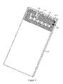
- Figure 1 is the schematic diagram of the spatial structure of the antenna grounded with U-shaped high-impedance surface metal strips in the present invention.
- Figure 2 is the schematic diagram of the U-shaped high-impedance surface unit set on the ground plate in the present invention.
- Figure 3 is the side view of the structure of the antenna grounded with U-shaped high-impedance surface metal strips in the present invention.
- Figure 4 is the schematic diagram of operating principle of the U-shaped high-impedance surface unit set on the ground plate in the present invention.
- Figure 5 is the schematic diagram of equivalent circuit of the U-shaped high-impedance surface unit set on the ground plate in the present invention.
- Figure 6 shows the comparison between the return loss test curves of the antenna with the U-shaped high-impedance surface units and the antenna without the U-shaped high-impedance surface units in the wireless communication unit of the present invention.
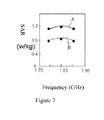
- Figure 7 shows the comparison between the SAR test curves of the antenna with the U-shaped high-impedance surface units and the antenna without the U-shaped high-impedance surface units in the wireless communication unit of the present invention.
- the antenna grounded with U-shaped high-impedance surface metal strips of the present invention comprises an antenna radiation unit 120 and its ground plate 110; wherein a plurality of high-impedance surface units are set on the ground plate 110 at relevant intervals; each high-impedance surface unit consists of three high-impedance surface metal strips 130 connected to each other in U shape; high-impedance surface through holes 160 are set in the high-impedance surface metal strips 130 at the bottom side of the U shape; and the high-impedance surface metal strips 130 between the high-impedance surface units are connected to each other by means of the high-impedance surface through holes 160.
- the present invention also provides a wireless communication unit, which in one embodiment comprises a case and an antenna for communications; the antenna is set inside the case and comprises an antenna radiation unit 120 and its ground plate 110; wherein a plurality of high-impedance surface units are set on the ground plate 110 at relevant intervals; each high-impedance surface unit consists of three high-impedance surface metal strips 130 connected to each other in U shape; high-impedance surface through holes 160 are set in the high-impedance surface metal strips 130 at the bottom side of the U shape; and the high-impedance surface metal strips 130 between the high-impedance surface units are connected to each other by means of the high-impedance surface through holes 160.
- Said high-impedance surface of the present invention refers to the surface structure that is built on the ground plate 110 of the antenna and can block the propagation of electromagnetic waves, that is, it has high-impedance characteristics to surface waves at a certain band; specifically, on one hand, it can suppress surface waves of frequencies propagated on its surface within its stopbands or does not support the propagation of surface waves of certain bands within its stopbands; on the other hand, it has the same-phase reflection effect for plane waves of incident frequencies perpendicular to its surface within its stopbands, that is, the phases of the reflection wave and incident wave do not change.
- said ground plate 110 refers to the whole PCB, and the high-impedance surface replaces the partial ground plate 110 under the antenna.
- the metal surface will make the phase of the plane wave changes for 180 degrees. If the ground plate 110 of the antenna is a complete metal plate, its surface propagates surface waves, and its impedance to surface waves is zero, no matter whether the frequency is within its stopband.
- the antenna grounded with U-shaped high-impedance surface metal strips and its wireless communication device of the present invention can suppress or block the propagation of surface waves along its surface on one hand and can also reflect the incident plane waves perpendicular to its surface on the other hand, because it has the high-impedance surface units connected to each other by means of a plurality of high-impedance surface through holes 160 and three high-impedance surface metal strips 130 form a U shape.
- the characteristic of the high-impedance surface to suppress surface waves is utilized, and said high-impedance surface is placed around the antenna, which reduces the radiation in the head direction (that is, the radiation of the antenna of the wireless communication device in the human body direction is reduced), decreases the SAR, and meanwhile, it does not weaken the energy of the plane wave, avoids the influence upon the signal strength, does not reduce the antenna radiation performance, does not affect the communication quality, and has generality and universal applicability.
- the antenna radiation unit 120 is a planar inverted F-type antenna, as shown in Figure 1 , there are two branches parts with open circuits at terminals in the antenna radiation unit 120. Its operating principle is one-fourth wavelength resonance; the wider and shorter one on the external side is the high-frequency branch part, and the narrower and longer one on the internal side is the low-frequency branch part. It is connected to the FR transmit/receive circuit of the PCB by means of the ground pin 140 of the antenna radiation unit 120 and the feed pin 150 of the antenna radiation unit 120.
- the ground plate 110 is a PCB; the high-impedance surface units are located on the surface of the PCB; the high-impedance surface through holes 160 are set to pass through the PCB; the copper-clad layer on the surface of the PCB is used to make the U-shaped high-impedance surface metal strips 130, and the through holes on the PCB are used to make the high-impedance surface through holes 160.
- the high-impedance surface through holes 160 are set to pass through the PCB, the U-shaped high-impedance surface metal strips 130 are electrically connected to the lower surface metal layer of the PCB by means of the high-impedance surface through holes 160 at the bottom side, to implement grounding of the high-impedance surface units.
- the U-shaped high-impedance surface metal strips 130 are set on the upper surface of the PCB, and the lower surface of the PCB is composed of a complete metal layer.
- the U-shaped high-impedance surface metal strips 130 are laid on the upper surface of the metal PCB as much as possible, especially in the lower region covered by the antenna radiation unit 120 to replace the original complete metal layer to serve as the new ground plane of the antenna radiation unit 120, to implement the transition of a zero-ohm ground plane to a ground plane with infinite impedance.
- the line breadth (B) of the high-impedance surface metal strip 130 is 1 mm
- the width (W) of the U-shaped high-impedance surface unit is 6 mm
- the height (H) of the U-shaped high-impedance surface unit is 8 mm
- the interval ( ⁇ ) between the high-impedance surface units is 0.5 mm.
- the U-shaped high-impedance surface units are set on the ground plate 110; wherein, the high-impedance surface metal strips 130 on the bottom side of the U shape are set to be in parallel with the rows formed by the high-impedance surface units.
- the U-shaped high-impedance surface units are set on the ground plate 110 to form columns; wherein, the high-impedance surface metal strips 130 on both sides of the U shape are set to be in parallel with the columns formed by the high-impedance surface units.
- the corresponding high-impedance metal strips between the U-shaped high-impedance surface units are set to be in parallel with each other.
- the high-impedance surface metal strips 130 at both sides and/or at the bottom in the U-shaped high-impedance surface units can form slanted rows or columns with the high-impedance surface units.
- the dielectric constant and thickness of the PCB will affect the structural size of the U-shaped metal strips, so during the design the length and width of the U-shaped metal strips and the intervals among the U-shaped metal strips can be adjusted properly to optimize the operating band of the high-impedance surface unit so that it is located within the transmit (Tx) channel range of the communication mode.
- the antenna and its wireless communication device of the present invention uses the U-shaped high-impedance surface metal strips 130 for grounding, and the electromagnetic characteristics of this structure can be described with IC components, capacitance and inductance. Its equivalent circuit parameter is presented with a parallel resonance LC circuit, as shown in Figure 5 , its function can be regarded as a two-dimensional electric filter to block the current from flowing along its surface.
- the surface impedance When lower than the resonance frequency, the surface impedance presents inductance; when higher than the resonance frequency, the surface impedance presents capacitance; at the proximity of the resonance frequency, the surface impedance is a very large value, which is equivalent to an infinite value.
- the resonance of the unit structure of the U-shaped metal strips and through holes is made be within the wireless Tx channel band of the communication mode, the structure will generate an infinite impedance within this band to block the pass of the RF surface current, so as to reduce the SAR within this band.
- the dotted line A shows the return loss test curve of the planar inverted F-type antenna when the high-impedance surface units are grounded; the solid line B shows the return loss test curve of the planar inverted F-type antenna when the high-impedance surface units are not grounded.
- the curve A shows that the U-shaped high-impedance surface metal strips 130 and the high-impedance surface through holes 160 do not have great influence. Therefore, the radiation performance is basically not affected.
- the dotted line A shows the SAR test curve of the planar inverted F-type antenna when the high-impedance surface units are grounded; the solid line B shows the SAR test curve of the planar inverted F-type antenna when the high-impedance surface units are not grounded.
- the curve A shows that the U-shaped high-impedance surface metal strips 130 and the high-impedance surface through holes 160 can effectively reduce the SAR, and the SAR of the same frequency can be reduced by about 30%.
- the antenna radiation unit 120 includes but is not limited to the planar inverted F-type antenna (e.g., it can be a multi-band antenna). Therefore, all technical schemes after such addition, decrease, replacement, change or improvement should fall within the protection scope defined by the accompany claims of the present invention.
Landscapes
- Physics & Mathematics (AREA)
- Optics & Photonics (AREA)
- Engineering & Computer Science (AREA)
- Computer Networks & Wireless Communication (AREA)
- Waveguide Aerials (AREA)
- Details Of Aerials (AREA)
- Support Of Aerials (AREA)
Abstract
Description
- Field of the Invention
- The present invention relates to the antenna field of wireless communication devices, and more specifically to an antenna grounded with U-shaped high-impedance surface metal strips and its wireless communication device.
- Background Technology
- The radio waves transmitted by a wireless communication device during communications expose the user to measurable radio frequency (RF) radiation. When a user uses a mobile terminal such as a mobile phone to make a call, the head of the user is always within the electromagnetic radiation field emitted by the mobile phone. Therefore, many countries including the People's Republic of China have issued complete and safe standards and specifications to manage and restrict the problem of exposure of RF energy. Here, the specific absorption rate (SAR) is an important evaluation parameter, which refers to the electromagnetic wave energy absorption rate of mobile phones or wireless communication products. Popularly, SAR is used to measure whether the influence of mobile phone radiation upon the body of a user, especially, the head of the user conforms to the relevant standards. SAR is also a unit for measuring the amount of RF energy absorbed by the body when using a mobile phone, and is used as a criterion for body protection.
- Presently, mobile terminals have been designed for use in such very rigid limitations, so various devices and methods are being developed to reduce the SAR, for example, materials for absorbing electromagnetic waves are added to mobile terminals, or metal parts are arranged properly to optimize the RF-induced current, complicated antenna design is used to reduce the SAR, and so on. However, these design methods are easily to be affected by the type of mobile terminals, so they do not have generality and universal applicability.
- Therefore, there is a need to improve and develop the prior art.
- Description of the Invention
- The purpose of the present invention is to provide an antenna grounded with U-shaped high-impedance surface metal strips and its wireless communication device, which not only can reduce the antenna radiation on human body, but also can avoid the influence upon communication quality, and furthermore, it has the universal applicability.
- The technical scheme of the present invention is as follows: an antenna grounded with U-shaped high-impedance surface metal strips, comprising an antenna radiation unit and its ground plate, wherein a plurality of high-impedance surface units are set on the ground plate at relevant intervals; each high-impedance surface unit consists of three high-impedance surface metal strips connected to each other in U shape; high-impedance surface through holes are set at the bottom side of the U shape; and the high-impedance surface units are connected to each other by means of the high-impedance surface through holes.
- In said antenna grounded with U-shaped high-impedance surface metal strips, the ground plate is a printed circuit board (PCB), the high-impedance surface units are located on the surface of the PCB, and the high-impedance surface through holes are set to pass through the PCB.
- In said antenna with grounded with U-shaped high-impedance surface metal strips, wherein the line breadth of the high-impedance surface metal strip is 1 mm, the width of the U-shaped high-impedance surface unit is 6 mm, the height of the U-shaped high-impedance surface unit is 8 mm, and the interval between the high-impedance surface units is 0.5 mm.
- In said antenna grounded with U-shaped high-impedance surface metal strips, the U-shaped high-impedance surface units are set on the ground plate to form rows.
- In said antenna grounded with U-shaped high-impedance surface metal strips, wherein the high-impedance surface metal strips on the bottom side of the U shape are set to be in parallel with the rows formed by the high-impedance surface units.
- In said antenna grounded with U-shaped high-impedance surface metal strips, wherein the U-shaped high-impedance surface units are set on the ground plate to form columns.
- In said antenna grounded with U-shaped high-impedance surface metal strips, wherein the high-impedance surface metal strips on both sides of the U shape is set to be in parallel with the columns formed by the high-impedance surface units.
- In said antenna grounded with U-shaped high-impedance surface metal strips, wherein the corresponding high-impedance metal strips between the U-shaped high-impedance surface units are set to be in parallel with each other.
- In said antenna grounded with U-shaped high-impedance surface metal strips, wherein characterized in that the antenna radiation unit is a planar inverted F-type antenna.
- A wireless communication device, which comprises a case and an antenna for communications, the antenna being set outside the case and comprising the antenna radiation unit and its ground plate; wherein a plurality of high-impedance surface units are set on the ground plate at relevant intervals; each high-impedance surface unit consists of three high-impedance surface metal strips connected to each other in U shape; high-impedance surface through holes are set at the bottom side of the U shape; and the high-impedance surface units are connected to each other by means of the high-impedance surface through holes.
- The antenna grounded with U-shaped high-impedance surface metal strips and its wireless communication device according to the present invention uses a plurality of high-impedance surface units connected to each other by means of high-impedance surface through holes and formed to a U shape by three high-impedance surface metal strips, such that on one hand the propagation of surface waves along its surface is suppressed or blocked, and on the other hand the same phase reflects the incident plane wave perpendicular to its surface; the capability of the high-impedance surface in suppressing surface waves is utilized, and said high-impedance surface is placed around the antenna, which reduces the radiation in the head direction (that is, the radiation of the antenna of the wireless communication device in the human body direction is reduced), decreases the SAR, and meanwhile, it does not weaken the energy of the plane wave, avoids the influence upon the signal strength, does not reduce the antenna radiation performance, does not affect the communication quality, and has generality and universal applicability.
- Brief Description of the Drawings
-
Figure 1 is the schematic diagram of the spatial structure of the antenna grounded with U-shaped high-impedance surface metal strips in the present invention. -
Figure 2 is the schematic diagram of the U-shaped high-impedance surface unit set on the ground plate in the present invention. -
Figure 3 is the side view of the structure of the antenna grounded with U-shaped high-impedance surface metal strips in the present invention. -
Figure 4 is the schematic diagram of operating principle of the U-shaped high-impedance surface unit set on the ground plate in the present invention. -
Figure 5 is the schematic diagram of equivalent circuit of the U-shaped high-impedance surface unit set on the ground plate in the present invention. -
Figure 6 shows the comparison between the return loss test curves of the antenna with the U-shaped high-impedance surface units and the antenna without the U-shaped high-impedance surface units in the wireless communication unit of the present invention. -
Figure 7 shows the comparison between the SAR test curves of the antenna with the U-shaped high-impedance surface units and the antenna without the U-shaped high-impedance surface units in the wireless communication unit of the present invention. - Particular Embodiments
- In the following, particular implementation modes and embodiments of the present invention will be further described with the combination of the drawings. The particular embodiments described here are used only for explaining the present invention and are not intended to limit the specific modes of implementing the present invention.
- In one embodiment as shown in
Figure 1 , the antenna grounded with U-shaped high-impedance surface metal strips of the present invention comprises anantenna radiation unit 120 and itsground plate 110; wherein a plurality of high-impedance surface units are set on theground plate 110 at relevant intervals; each high-impedance surface unit consists of three high-impedancesurface metal strips 130 connected to each other in U shape; high-impedance surface throughholes 160 are set in the high-impedancesurface metal strips 130 at the bottom side of the U shape; and the high-impedancesurface metal strips 130 between the high-impedance surface units are connected to each other by means of the high-impedance surface throughholes 160. - Based on the antenna grounded with U-shaped high-impedance
surface metal strips 130, the present invention also provides a wireless communication unit, which in one embodiment comprises a case and an antenna for communications; the antenna is set inside the case and comprises anantenna radiation unit 120 and itsground plate 110; wherein a plurality of high-impedance surface units are set on theground plate 110 at relevant intervals; each high-impedance surface unit consists of three high-impedancesurface metal strips 130 connected to each other in U shape; high-impedance surface throughholes 160 are set in the high-impedancesurface metal strips 130 at the bottom side of the U shape; and the high-impedancesurface metal strips 130 between the high-impedance surface units are connected to each other by means of the high-impedance surface throughholes 160. - Said high-impedance surface of the present invention refers to the surface structure that is built on the
ground plate 110 of the antenna and can block the propagation of electromagnetic waves, that is, it has high-impedance characteristics to surface waves at a certain band; specifically, on one hand, it can suppress surface waves of frequencies propagated on its surface within its stopbands or does not support the propagation of surface waves of certain bands within its stopbands; on the other hand, it has the same-phase reflection effect for plane waves of incident frequencies perpendicular to its surface within its stopbands, that is, the phases of the reflection wave and incident wave do not change. Specifically, saidground plate 110 refers to the whole PCB, and the high-impedance surface replaces thepartial ground plate 110 under the antenna. - For the incident plane wave perpendicular to the metal surface, the metal surface will make the phase of the plane wave changes for 180 degrees. If the
ground plate 110 of the antenna is a complete metal plate, its surface propagates surface waves, and its impedance to surface waves is zero, no matter whether the frequency is within its stopband. Compared with an antenna grounded with a complete metal plate and its wireless communication device in the prior art, the antenna grounded with U-shaped high-impedance surface metal strips and its wireless communication device of the present invention can suppress or block the propagation of surface waves along its surface on one hand and can also reflect the incident plane waves perpendicular to its surface on the other hand, because it has the high-impedance surface units connected to each other by means of a plurality of high-impedance surface throughholes 160 and three high-impedancesurface metal strips 130 form a U shape. The characteristic of the high-impedance surface to suppress surface waves is utilized, and said high-impedance surface is placed around the antenna, which reduces the radiation in the head direction (that is, the radiation of the antenna of the wireless communication device in the human body direction is reduced), decreases the SAR, and meanwhile, it does not weaken the energy of the plane wave, avoids the influence upon the signal strength, does not reduce the antenna radiation performance, does not affect the communication quality, and has generality and universal applicability. - Suppose that the
antenna radiation unit 120 is a planar inverted F-type antenna, as shown inFigure 1 , there are two branches parts with open circuits at terminals in theantenna radiation unit 120. Its operating principle is one-fourth wavelength resonance; the wider and shorter one on the external side is the high-frequency branch part, and the narrower and longer one on the internal side is the low-frequency branch part. It is connected to the FR transmit/receive circuit of the PCB by means of theground pin 140 of theantenna radiation unit 120 and thefeed pin 150 of theantenna radiation unit 120. - In a preferred embodiment of the antenna grounded with U-shaped high-impedance
surface metal strips 130 and its wireless communication device of the present invention, as shown inFigure 2 , theground plate 110 is a PCB; the high-impedance surface units are located on the surface of the PCB; the high-impedance surface throughholes 160 are set to pass through the PCB; the copper-clad layer on the surface of the PCB is used to make the U-shaped high-impedancesurface metal strips 130, and the through holes on the PCB are used to make the high-impedance surface throughholes 160. - Preferably, as shown in
Figure 3 , the high-impedance surface throughholes 160 are set to pass through the PCB, the U-shaped high-impedancesurface metal strips 130 are electrically connected to the lower surface metal layer of the PCB by means of the high-impedance surface throughholes 160 at the bottom side, to implement grounding of the high-impedance surface units. - Specifically, the U-shaped high-impedance
surface metal strips 130 are set on the upper surface of the PCB, and the lower surface of the PCB is composed of a complete metal layer. The U-shaped high-impedancesurface metal strips 130 are laid on the upper surface of the metal PCB as much as possible, especially in the lower region covered by theantenna radiation unit 120 to replace the original complete metal layer to serve as the new ground plane of theantenna radiation unit 120, to implement the transition of a zero-ohm ground plane to a ground plane with infinite impedance. - Preferably, as shown in
Figure 2 , the line breadth (B) of the high-impedancesurface metal strip 130 is 1 mm, the width (W) of the U-shaped high-impedance surface unit is 6 mm, the height (H) of the U-shaped high-impedance surface unit is 8 mm, and the interval (δ) between the high-impedance surface units is 0.5 mm. - Further, the U-shaped high-impedance surface units are set on the
ground plate 110; wherein, the high-impedancesurface metal strips 130 on the bottom side of the U shape are set to be in parallel with the rows formed by the high-impedance surface units. And the U-shaped high-impedance surface units are set on theground plate 110 to form columns; wherein, the high-impedancesurface metal strips 130 on both sides of the U shape are set to be in parallel with the columns formed by the high-impedance surface units. - Preferably, the corresponding high-impedance metal strips between the U-shaped high-impedance surface units are set to be in parallel with each other.
- Of course, the high-impedance
surface metal strips 130 at both sides and/or at the bottom in the U-shaped high-impedance surface units can form slanted rows or columns with the high-impedance surface units. - The dielectric constant and thickness of the PCB will affect the structural size of the U-shaped metal strips, so during the design the length and width of the U-shaped metal strips and the intervals among the U-shaped metal strips can be adjusted properly to optimize the operating band of the high-impedance surface unit so that it is located within the transmit (Tx) channel range of the communication mode.
- The antenna and its wireless communication device of the present invention uses the U-shaped high-impedance
surface metal strips 130 for grounding, and the electromagnetic characteristics of this structure can be described with IC components, capacitance and inductance. Its equivalent circuit parameter is presented with a parallel resonance LC circuit, as shown inFigure 5 , its function can be regarded as a two-dimensional electric filter to block the current from flowing along its surface. - As shown in
Figure 4 , when the U-shaped metal strips and the ground through holes interact with electromagnetic waves, an induced current is generated on the U-shaped metal strips, which is in parallel with the voltage function at the top surface, resulting in accumulative charges at both ends of the U-shaped metal strips. Therefore, it can be equivalent to the capacitive effect. However, charges flow from and to the metal through holes and the lower surface of the PCB to form a current loop, which is connected to the magnetic field and inductance.Figure 4 shows its capacitance and inductance, andFigure 5 shows its equivalent resonance circuit. - When lower than the resonance frequency, the surface impedance presents inductance; when higher than the resonance frequency, the surface impedance presents capacitance; at the proximity of the resonance frequency, the surface impedance is a very large value, which is equivalent to an infinite value. During design, if the resonance of the unit structure of the U-shaped metal strips and through holes is made be within the wireless Tx channel band of the communication mode, the structure will generate an infinite impedance within this band to block the pass of the RF surface current, so as to reduce the SAR within this band.
- As shown in
Figure 6 , the dotted line A shows the return loss test curve of the planar inverted F-type antenna when the high-impedance surface units are grounded; the solid line B shows the return loss test curve of the planar inverted F-type antenna when the high-impedance surface units are not grounded. The curve A shows that the U-shaped high-impedance surface metal strips 130 and the high-impedance surface throughholes 160 do not have great influence. Therefore, the radiation performance is basically not affected. - As shown in
Figure 7 , the dotted line A shows the SAR test curve of the planar inverted F-type antenna when the high-impedance surface units are grounded; the solid line B shows the SAR test curve of the planar inverted F-type antenna when the high-impedance surface units are not grounded. The curve A shows that the U-shaped high-impedance surface metal strips 130 and the high-impedance surface throughholes 160 can effectively reduce the SAR, and the SAR of the same frequency can be reduced by about 30%. - It should be understood that the above are only preferred embodiments of the present invention and are not intended to limit the technical scheme of the present invention. Without departing from the spirit and principle of the present invention, those skilled in the art can add, decrease, replace, change or improve the present invention according to the preceding descriptions, for example, the
antenna radiation unit 120 includes but is not limited to the planar inverted F-type antenna (e.g., it can be a multi-band antenna). Therefore, all technical schemes after such addition, decrease, replacement, change or improvement should fall within the protection scope defined by the accompany claims of the present invention.
Claims (10)
- An antenna grounded with U-shaped high-impedance surface metal strips, comprising an antenna radiation unit and its ground plate, wherein a plurality of high-impedance surface units are set on the ground plate at relevant intervals; each high-impedance surface unit consists of three high-impedance surface metal strips connected to each other in U shape; high-impedance surface through holes are set at the bottom side of the U shape; and the high-impedance surface units are connected to each other by means of the high-impedance surface through holes.
- The antenna grounded with U-shaped high-impedance surface metal strips according to claim 1, wherein the ground plate is a printed circuit board (PCB), the high-impedance surface units are located on the surface of the PCB, and the high-impedance surface through holes are set to pass through the PCB.
- The antenna grounded with U-shaped high-impedance surface metal strips according to claim 1, wherein the line breadth of the high-impedance surface metal strip is 1 mm, the width of the U-shaped high-impedance surface unit is 6 mm, the height of the U-shaped high-impedance surface unit is 8 mm, and the interval between the high-impedance surface units is 0.5 mm.
- The antenna grounded with U-shaped high-impedance surface metal strips according to claim 1, wherein the U-shaped high-impedance surface units are set on the ground plate to form rows.
- The antenna grounded with U-shaped high-impedance surface metal strips according to claim 4, wherein the high-impedance surface metal strips on the bottom side of the U shape are set to be in parallel with the rows formed by the high-impedance surface units.
- The antenna grounded with U-shaped high-impedance surface metal strips according to claim 1, wherein the U-shaped high-impedance surface units are set on the ground plate to form columns.
- The antenna grounded with U-shaped high-impedance surface metal strips according to claim 6, wherein the high-impedance surface metal strips on the both sides of the U shape are set to be in parallel with the columns formed by the high-impedance surface units.
- The antenna grounded with U-shaped high-impedance surface metal strips according to claim 1, wherein the corresponding high-impedance metal strips between the U-shaped high-impedance surface units are set to be in parallel with each other.
- The antenna grounded with U-shaped high-impedance surface metal strips according to claims 1 through 8, wherein the antenna radiation unit is a planar inverted F-type antenna.
- A wireless communication device, which comprises a case and an antenna for communications, the antenna being set outside the case and comprising an antenna radiation unit and its ground plate, wherein a plurality of high-impedance surface units are set on the ground plate at relevant intervals; each high-impedance surface unit consists of three high-impedance surface metal strips connected to each other in U shape; high-impedance surface through holes are set at the bottom side of the U shape; and the high-impedance surface units are connected to each other by means of the high-impedance surface through holes.
Applications Claiming Priority (2)
| Application Number | Priority Date | Filing Date | Title |
|---|---|---|---|
| CN2010105769252A CN102044752B (en) | 2010-12-07 | 2010-12-07 | Antenna with grounded U-shaped high-impedance surface metal strips and wireless communication device |
| PCT/CN2011/081837 WO2012075868A1 (en) | 2010-12-07 | 2011-11-05 | Grounded antenna having u-shaped high-impedance surface metal strips and wireless communication device having said antenna |
Publications (3)
| Publication Number | Publication Date |
|---|---|
| EP2650968A1 true EP2650968A1 (en) | 2013-10-16 |
| EP2650968A4 EP2650968A4 (en) | 2017-07-19 |
| EP2650968B1 EP2650968B1 (en) | 2019-04-10 |
Family
ID=43910673
Family Applications (1)
| Application Number | Title | Priority Date | Filing Date |
|---|---|---|---|
| EP11847282.8A Not-in-force EP2650968B1 (en) | 2010-12-07 | 2011-11-05 | Grounded antenna having u-shaped high-impedance surface metal strips and wireless communication device having said antenna |
Country Status (5)
| Country | Link |
|---|---|
| US (1) | US9147941B2 (en) |
| EP (1) | EP2650968B1 (en) |
| CN (1) | CN102044752B (en) |
| ES (1) | ES2733736T3 (en) |
| WO (1) | WO2012075868A1 (en) |
Cited By (1)
| Publication number | Priority date | Publication date | Assignee | Title |
|---|---|---|---|---|
| WO2015076849A1 (en) * | 2013-11-25 | 2015-05-28 | Hewlett-Packard Development Company, L.P. | Antenna devices |
Families Citing this family (6)
| Publication number | Priority date | Publication date | Assignee | Title |
|---|---|---|---|---|
| CN102044752B (en) * | 2010-12-07 | 2013-10-23 | 惠州Tcl移动通信有限公司 | Antenna with grounded U-shaped high-impedance surface metal strips and wireless communication device |
| US8842055B2 (en) * | 2011-05-26 | 2014-09-23 | Texas Instruments Incorporated | High impedance surface |
| CN105720374A (en) * | 2016-04-08 | 2016-06-29 | 东南大学 | Three-polarized half-slot antenna of grating slit and ground coaxial feeding plated through hole stepped-impedance |
| TWI621303B (en) * | 2017-01-23 | 2018-04-11 | 廣達電腦股份有限公司 | Mobile device |
| EP3918664B1 (en) | 2019-03-14 | 2023-10-11 | Huawei Technologies Co., Ltd. | Redirecting structure for electromagnetic waves |
| CN117014923A (en) * | 2022-04-28 | 2023-11-07 | 中兴通讯股份有限公司 | Test equipment and test systems |
Family Cites Families (12)
| Publication number | Priority date | Publication date | Assignee | Title |
|---|---|---|---|---|
| US5400041A (en) * | 1991-07-26 | 1995-03-21 | Strickland; Peter C. | Radiating element incorporating impedance transformation capabilities |
| US6426722B1 (en) * | 2000-03-08 | 2002-07-30 | Hrl Laboratories, Llc | Polarization converting radio frequency reflecting surface |
| GB0101667D0 (en) * | 2001-01-23 | 2001-03-07 | Koninkl Philips Electronics Nv | Antenna arrangement |
| WO2002087012A1 (en) * | 2001-04-24 | 2002-10-31 | Telefonaktiebolaget Lm Ericsson | Pifa antenna with higp structure |
| TWI249875B (en) * | 2003-09-19 | 2006-02-21 | Univ Nat Taiwan Science Tech | Method and apparatus for improving antenna radiation patterns |
| US7190315B2 (en) * | 2003-12-18 | 2007-03-13 | Intel Corporation | Frequency selective surface to suppress surface currents |
| CN101102009B (en) * | 2006-07-03 | 2011-10-05 | 光宝科技股份有限公司 | UWB Antenna Structure |
| CN201084827Y (en) * | 2007-09-07 | 2008-07-09 | 达昌电子科技(苏州)有限公司 | A single-pole antenna module |
| CN101188329B (en) * | 2007-12-04 | 2011-06-22 | 同济大学 | A dual-frequency ultra-thin highly directional resonant cavity antenna |
| CN101320845B (en) * | 2007-12-24 | 2012-11-21 | 中国科学院光电技术研究所 | Design method of high-directivity antenna adopting combination of electromagnetic band gap structure and metal grid structure |
| CN201946752U (en) * | 2010-12-07 | 2011-08-24 | 惠州Tcl移动通信有限公司 | Antenna with grounded U-shaped high-impedance surface metal strips and wireless communication device adopting same |
| CN102044752B (en) * | 2010-12-07 | 2013-10-23 | 惠州Tcl移动通信有限公司 | Antenna with grounded U-shaped high-impedance surface metal strips and wireless communication device |
-
2010
- 2010-12-07 CN CN2010105769252A patent/CN102044752B/en not_active Expired - Fee Related
-
2011
- 2011-11-05 ES ES11847282T patent/ES2733736T3/en active Active
- 2011-11-05 EP EP11847282.8A patent/EP2650968B1/en not_active Not-in-force
- 2011-11-05 US US13/810,795 patent/US9147941B2/en not_active Expired - Fee Related
- 2011-11-05 WO PCT/CN2011/081837 patent/WO2012075868A1/en not_active Ceased
Non-Patent Citations (1)
| Title |
|---|
| See references of WO2012075868A1 * |
Cited By (2)
| Publication number | Priority date | Publication date | Assignee | Title |
|---|---|---|---|---|
| WO2015076849A1 (en) * | 2013-11-25 | 2015-05-28 | Hewlett-Packard Development Company, L.P. | Antenna devices |
| US10249939B2 (en) | 2013-11-25 | 2019-04-02 | Hewlett-Packard Development Company, L.P. | Antenna devices |
Also Published As
| Publication number | Publication date |
|---|---|
| CN102044752B (en) | 2013-10-23 |
| EP2650968B1 (en) | 2019-04-10 |
| EP2650968A4 (en) | 2017-07-19 |
| US20130120212A1 (en) | 2013-05-16 |
| US9147941B2 (en) | 2015-09-29 |
| WO2012075868A1 (en) | 2012-06-14 |
| CN102044752A (en) | 2011-05-04 |
| ES2733736T3 (en) | 2019-12-02 |
Similar Documents
| Publication | Publication Date | Title |
|---|---|---|
| US9768507B2 (en) | Antenna devices having frequency-dependent connection to electrical ground | |
| US9160069B2 (en) | Grounded antenna with cross-shaped high-impedance surface metal strips and wireless communication device having said antenna | |
| US9147941B2 (en) | Antenna grounded with U-shaped high-impedance surface metal strips and its wireless communication device | |
| GB2510318A (en) | Antenna device with reduced specific absorption rate (SAR) characteristics | |
| EP2151012A1 (en) | Antenna | |
| CN101877433B (en) | Multi-frequency antenna and wireless communication device applying same | |
| KR101710434B1 (en) | Antenna devices having frequency-dependent connection to electrical ground | |
| CN102904065A (en) | Wave absorbing device and wireless terminal | |
| EP1310014B1 (en) | Wireless terminal | |
| US12183995B2 (en) | Antenna structure and electronic apparatus | |
| US7760147B2 (en) | Antenna and mobile communication terminal comprising the same | |
| CN201918509U (en) | Antenna with cross-shaped high-impedance surface metal strips for grounding and wireless communication device thereof | |
| US20180138579A1 (en) | Antenna Apparatus and Terminal | |
| EP1364428B1 (en) | Wireless terminal | |
| US10181649B2 (en) | Antenna and mobile terminal | |
| EP3261178B1 (en) | Slot antenna | |
| CN201946752U (en) | Antenna with grounded U-shaped high-impedance surface metal strips and wireless communication device adopting same | |
| CN210167509U (en) | Wave-absorbing structure | |
| CN102208925B (en) | Low near-field radiation mobile communication device | |
| Pelletti et al. | Techniques for reducing the SAR in mobile devices by using graphene-type absorbing materials | |
| Taguchi et al. | Rectangular microstrip antenna excited by monopole antenna mounted on finite dielectric substrate | |
| KR20050087492A (en) | Variable ground method of reducing specific absorption rate of wireless communication equipments | |
| Messaoudi et al. | Synthetic Study of Different Solutions to Reduce the SAR in the Human Head | |
| US8378896B2 (en) | Wide band antenna | |
| Kim et al. | Design of a 2.3 GHz Band Mobile-WiMAX MIMO Antenna using Split Ring Resonator |
Legal Events
| Date | Code | Title | Description |
|---|---|---|---|
| PUAI | Public reference made under article 153(3) epc to a published international application that has entered the european phase |
Free format text: ORIGINAL CODE: 0009012 |
|
| 17P | Request for examination filed |
Effective date: 20130705 |
|
| AK | Designated contracting states |
Kind code of ref document: A1 Designated state(s): AL AT BE BG CH CY CZ DE DK EE ES FI FR GB GR HR HU IE IS IT LI LT LU LV MC MK MT NL NO PL PT RO RS SE SI SK SM TR |
|
| DAX | Request for extension of the european patent (deleted) | ||
| REG | Reference to a national code |
Ref country code: DE Ref legal event code: R079 Ref document number: 602011058036 Country of ref document: DE Free format text: PREVIOUS MAIN CLASS: H01Q0001480000 Ipc: H01Q0015000000 |
|
| RA4 | Supplementary search report drawn up and despatched (corrected) |
Effective date: 20170620 |
|
| RIC1 | Information provided on ipc code assigned before grant |
Ipc: H01Q 1/24 20060101ALI20170613BHEP Ipc: H01Q 15/00 20060101AFI20170613BHEP Ipc: H01Q 9/04 20060101ALI20170613BHEP |
|
| STAA | Information on the status of an ep patent application or granted ep patent |
Free format text: STATUS: EXAMINATION IS IN PROGRESS |
|
| 17Q | First examination report despatched |
Effective date: 20180522 |
|
| GRAP | Despatch of communication of intention to grant a patent |
Free format text: ORIGINAL CODE: EPIDOSNIGR1 |
|
| STAA | Information on the status of an ep patent application or granted ep patent |
Free format text: STATUS: GRANT OF PATENT IS INTENDED |
|
| INTG | Intention to grant announced |
Effective date: 20181122 |
|
| GRAS | Grant fee paid |
Free format text: ORIGINAL CODE: EPIDOSNIGR3 |
|
| GRAA | (expected) grant |
Free format text: ORIGINAL CODE: 0009210 |
|
| STAA | Information on the status of an ep patent application or granted ep patent |
Free format text: STATUS: THE PATENT HAS BEEN GRANTED |
|
| AK | Designated contracting states |
Kind code of ref document: B1 Designated state(s): AL AT BE BG CH CY CZ DE DK EE ES FI FR GB GR HR HU IE IS IT LI LT LU LV MC MK MT NL NO PL PT RO RS SE SI SK SM TR |
|
| REG | Reference to a national code |
Ref country code: GB Ref legal event code: FG4D |
|
| REG | Reference to a national code |
Ref country code: CH Ref legal event code: EP Ref country code: AT Ref legal event code: REF Ref document number: 1119944 Country of ref document: AT Kind code of ref document: T Effective date: 20190415 |
|
| REG | Reference to a national code |
Ref country code: IE Ref legal event code: FG4D |
|
| REG | Reference to a national code |
Ref country code: DE Ref legal event code: R096 Ref document number: 602011058036 Country of ref document: DE |
|
| REG | Reference to a national code |
Ref country code: NL Ref legal event code: MP Effective date: 20190410 |
|
| REG | Reference to a national code |
Ref country code: LT Ref legal event code: MG4D |
|
| REG | Reference to a national code |
Ref country code: AT Ref legal event code: MK05 Ref document number: 1119944 Country of ref document: AT Kind code of ref document: T Effective date: 20190410 |
|
| PG25 | Lapsed in a contracting state [announced via postgrant information from national office to epo] |
Ref country code: NL Free format text: LAPSE BECAUSE OF FAILURE TO SUBMIT A TRANSLATION OF THE DESCRIPTION OR TO PAY THE FEE WITHIN THE PRESCRIBED TIME-LIMIT Effective date: 20190410 |
|
| PG25 | Lapsed in a contracting state [announced via postgrant information from national office to epo] |
Ref country code: FI Free format text: LAPSE BECAUSE OF FAILURE TO SUBMIT A TRANSLATION OF THE DESCRIPTION OR TO PAY THE FEE WITHIN THE PRESCRIBED TIME-LIMIT Effective date: 20190410 Ref country code: SE Free format text: LAPSE BECAUSE OF FAILURE TO SUBMIT A TRANSLATION OF THE DESCRIPTION OR TO PAY THE FEE WITHIN THE PRESCRIBED TIME-LIMIT Effective date: 20190410 Ref country code: LT Free format text: LAPSE BECAUSE OF FAILURE TO SUBMIT A TRANSLATION OF THE DESCRIPTION OR TO PAY THE FEE WITHIN THE PRESCRIBED TIME-LIMIT Effective date: 20190410 Ref country code: PT Free format text: LAPSE BECAUSE OF FAILURE TO SUBMIT A TRANSLATION OF THE DESCRIPTION OR TO PAY THE FEE WITHIN THE PRESCRIBED TIME-LIMIT Effective date: 20190910 Ref country code: AL Free format text: LAPSE BECAUSE OF FAILURE TO SUBMIT A TRANSLATION OF THE DESCRIPTION OR TO PAY THE FEE WITHIN THE PRESCRIBED TIME-LIMIT Effective date: 20190410 Ref country code: NO Free format text: LAPSE BECAUSE OF FAILURE TO SUBMIT A TRANSLATION OF THE DESCRIPTION OR TO PAY THE FEE WITHIN THE PRESCRIBED TIME-LIMIT Effective date: 20190710 Ref country code: HR Free format text: LAPSE BECAUSE OF FAILURE TO SUBMIT A TRANSLATION OF THE DESCRIPTION OR TO PAY THE FEE WITHIN THE PRESCRIBED TIME-LIMIT Effective date: 20190410 |
|
| PG25 | Lapsed in a contracting state [announced via postgrant information from national office to epo] |
Ref country code: LV Free format text: LAPSE BECAUSE OF FAILURE TO SUBMIT A TRANSLATION OF THE DESCRIPTION OR TO PAY THE FEE WITHIN THE PRESCRIBED TIME-LIMIT Effective date: 20190410 Ref country code: PL Free format text: LAPSE BECAUSE OF FAILURE TO SUBMIT A TRANSLATION OF THE DESCRIPTION OR TO PAY THE FEE WITHIN THE PRESCRIBED TIME-LIMIT Effective date: 20190410 Ref country code: GR Free format text: LAPSE BECAUSE OF FAILURE TO SUBMIT A TRANSLATION OF THE DESCRIPTION OR TO PAY THE FEE WITHIN THE PRESCRIBED TIME-LIMIT Effective date: 20190711 Ref country code: RS Free format text: LAPSE BECAUSE OF FAILURE TO SUBMIT A TRANSLATION OF THE DESCRIPTION OR TO PAY THE FEE WITHIN THE PRESCRIBED TIME-LIMIT Effective date: 20190410 Ref country code: BG Free format text: LAPSE BECAUSE OF FAILURE TO SUBMIT A TRANSLATION OF THE DESCRIPTION OR TO PAY THE FEE WITHIN THE PRESCRIBED TIME-LIMIT Effective date: 20190710 |
|
| REG | Reference to a national code |
Ref country code: ES Ref legal event code: FG2A Ref document number: 2733736 Country of ref document: ES Kind code of ref document: T3 Effective date: 20191202 |
|
| PG25 | Lapsed in a contracting state [announced via postgrant information from national office to epo] |
Ref country code: AT Free format text: LAPSE BECAUSE OF FAILURE TO SUBMIT A TRANSLATION OF THE DESCRIPTION OR TO PAY THE FEE WITHIN THE PRESCRIBED TIME-LIMIT Effective date: 20190410 Ref country code: IS Free format text: LAPSE BECAUSE OF FAILURE TO SUBMIT A TRANSLATION OF THE DESCRIPTION OR TO PAY THE FEE WITHIN THE PRESCRIBED TIME-LIMIT Effective date: 20190810 |
|
| REG | Reference to a national code |
Ref country code: DE Ref legal event code: R097 Ref document number: 602011058036 Country of ref document: DE |
|
| PG25 | Lapsed in a contracting state [announced via postgrant information from national office to epo] |
Ref country code: RO Free format text: LAPSE BECAUSE OF FAILURE TO SUBMIT A TRANSLATION OF THE DESCRIPTION OR TO PAY THE FEE WITHIN THE PRESCRIBED TIME-LIMIT Effective date: 20190410 Ref country code: SK Free format text: LAPSE BECAUSE OF FAILURE TO SUBMIT A TRANSLATION OF THE DESCRIPTION OR TO PAY THE FEE WITHIN THE PRESCRIBED TIME-LIMIT Effective date: 20190410 Ref country code: CZ Free format text: LAPSE BECAUSE OF FAILURE TO SUBMIT A TRANSLATION OF THE DESCRIPTION OR TO PAY THE FEE WITHIN THE PRESCRIBED TIME-LIMIT Effective date: 20190410 Ref country code: DK Free format text: LAPSE BECAUSE OF FAILURE TO SUBMIT A TRANSLATION OF THE DESCRIPTION OR TO PAY THE FEE WITHIN THE PRESCRIBED TIME-LIMIT Effective date: 20190410 Ref country code: EE Free format text: LAPSE BECAUSE OF FAILURE TO SUBMIT A TRANSLATION OF THE DESCRIPTION OR TO PAY THE FEE WITHIN THE PRESCRIBED TIME-LIMIT Effective date: 20190410 |
|
| PLBE | No opposition filed within time limit |
Free format text: ORIGINAL CODE: 0009261 |
|
| STAA | Information on the status of an ep patent application or granted ep patent |
Free format text: STATUS: NO OPPOSITION FILED WITHIN TIME LIMIT |
|
| PG25 | Lapsed in a contracting state [announced via postgrant information from national office to epo] |
Ref country code: SM Free format text: LAPSE BECAUSE OF FAILURE TO SUBMIT A TRANSLATION OF THE DESCRIPTION OR TO PAY THE FEE WITHIN THE PRESCRIBED TIME-LIMIT Effective date: 20190410 |
|
| 26N | No opposition filed |
Effective date: 20200113 |
|
| PG25 | Lapsed in a contracting state [announced via postgrant information from national office to epo] |
Ref country code: TR Free format text: LAPSE BECAUSE OF FAILURE TO SUBMIT A TRANSLATION OF THE DESCRIPTION OR TO PAY THE FEE WITHIN THE PRESCRIBED TIME-LIMIT Effective date: 20190410 |
|
| PG25 | Lapsed in a contracting state [announced via postgrant information from national office to epo] |
Ref country code: SI Free format text: LAPSE BECAUSE OF FAILURE TO SUBMIT A TRANSLATION OF THE DESCRIPTION OR TO PAY THE FEE WITHIN THE PRESCRIBED TIME-LIMIT Effective date: 20190410 |
|
| REG | Reference to a national code |
Ref country code: CH Ref legal event code: PL |
|
| PG25 | Lapsed in a contracting state [announced via postgrant information from national office to epo] |
Ref country code: MC Free format text: LAPSE BECAUSE OF FAILURE TO SUBMIT A TRANSLATION OF THE DESCRIPTION OR TO PAY THE FEE WITHIN THE PRESCRIBED TIME-LIMIT Effective date: 20190410 Ref country code: LI Free format text: LAPSE BECAUSE OF NON-PAYMENT OF DUE FEES Effective date: 20191130 Ref country code: CH Free format text: LAPSE BECAUSE OF NON-PAYMENT OF DUE FEES Effective date: 20191130 Ref country code: LU Free format text: LAPSE BECAUSE OF NON-PAYMENT OF DUE FEES Effective date: 20191105 |
|
| REG | Reference to a national code |
Ref country code: BE Ref legal event code: MM Effective date: 20191130 |
|
| PG25 | Lapsed in a contracting state [announced via postgrant information from national office to epo] |
Ref country code: IE Free format text: LAPSE BECAUSE OF NON-PAYMENT OF DUE FEES Effective date: 20191105 |
|
| PG25 | Lapsed in a contracting state [announced via postgrant information from national office to epo] |
Ref country code: BE Free format text: LAPSE BECAUSE OF NON-PAYMENT OF DUE FEES Effective date: 20191130 |
|
| PGFP | Annual fee paid to national office [announced via postgrant information from national office to epo] |
Ref country code: GB Payment date: 20201123 Year of fee payment: 10 Ref country code: FR Payment date: 20201120 Year of fee payment: 10 Ref country code: DE Payment date: 20201119 Year of fee payment: 10 Ref country code: IT Payment date: 20201124 Year of fee payment: 10 |
|
| PG25 | Lapsed in a contracting state [announced via postgrant information from national office to epo] |
Ref country code: CY Free format text: LAPSE BECAUSE OF FAILURE TO SUBMIT A TRANSLATION OF THE DESCRIPTION OR TO PAY THE FEE WITHIN THE PRESCRIBED TIME-LIMIT Effective date: 20190410 |
|
| PGFP | Annual fee paid to national office [announced via postgrant information from national office to epo] |
Ref country code: ES Payment date: 20210122 Year of fee payment: 10 |
|
| PG25 | Lapsed in a contracting state [announced via postgrant information from national office to epo] |
Ref country code: HU Free format text: LAPSE BECAUSE OF FAILURE TO SUBMIT A TRANSLATION OF THE DESCRIPTION OR TO PAY THE FEE WITHIN THE PRESCRIBED TIME-LIMIT; INVALID AB INITIO Effective date: 20111105 Ref country code: MT Free format text: LAPSE BECAUSE OF FAILURE TO SUBMIT A TRANSLATION OF THE DESCRIPTION OR TO PAY THE FEE WITHIN THE PRESCRIBED TIME-LIMIT Effective date: 20190410 |
|
| REG | Reference to a national code |
Ref country code: DE Ref legal event code: R119 Ref document number: 602011058036 Country of ref document: DE |
|
| PG25 | Lapsed in a contracting state [announced via postgrant information from national office to epo] |
Ref country code: MK Free format text: LAPSE BECAUSE OF FAILURE TO SUBMIT A TRANSLATION OF THE DESCRIPTION OR TO PAY THE FEE WITHIN THE PRESCRIBED TIME-LIMIT Effective date: 20190410 |
|
| GBPC | Gb: european patent ceased through non-payment of renewal fee |
Effective date: 20211105 |
|
| PG25 | Lapsed in a contracting state [announced via postgrant information from national office to epo] |
Ref country code: GB Free format text: LAPSE BECAUSE OF NON-PAYMENT OF DUE FEES Effective date: 20211105 Ref country code: DE Free format text: LAPSE BECAUSE OF NON-PAYMENT OF DUE FEES Effective date: 20220601 |
|
| PG25 | Lapsed in a contracting state [announced via postgrant information from national office to epo] |
Ref country code: FR Free format text: LAPSE BECAUSE OF NON-PAYMENT OF DUE FEES Effective date: 20211130 |
|
| PG25 | Lapsed in a contracting state [announced via postgrant information from national office to epo] |
Ref country code: IT Free format text: LAPSE BECAUSE OF NON-PAYMENT OF DUE FEES Effective date: 20211105 |
|
| REG | Reference to a national code |
Ref country code: ES Ref legal event code: FD2A Effective date: 20230223 |
|
| PG25 | Lapsed in a contracting state [announced via postgrant information from national office to epo] |
Ref country code: ES Free format text: LAPSE BECAUSE OF NON-PAYMENT OF DUE FEES Effective date: 20211106 |