EP2650901A1 - Charged particle beam apparatus and method of irradiating charged particle beam - Google Patents
Charged particle beam apparatus and method of irradiating charged particle beam Download PDFInfo
- Publication number
- EP2650901A1 EP2650901A1 EP11847394.1A EP11847394A EP2650901A1 EP 2650901 A1 EP2650901 A1 EP 2650901A1 EP 11847394 A EP11847394 A EP 11847394A EP 2650901 A1 EP2650901 A1 EP 2650901A1
- Authority
- EP
- European Patent Office
- Prior art keywords
- sample
- ion beam
- electrode unit
- charged particle
- ion
- Prior art date
- Legal status (The legal status is an assumption and is not a legal conclusion. Google has not performed a legal analysis and makes no representation as to the accuracy of the status listed.)
- Withdrawn
Links
Images





Classifications
-
- H—ELECTRICITY
- H01—ELECTRIC ELEMENTS
- H01J—ELECTRIC DISCHARGE TUBES OR DISCHARGE LAMPS
- H01J37/00—Discharge tubes with provision for introducing objects or material to be exposed to the discharge, e.g. for the purpose of examination or processing thereof
- H01J37/02—Details
- H01J37/04—Arrangements of electrodes and associated parts for generating or controlling the discharge, e.g. electron-optical arrangement or ion-optical arrangement
- H01J37/147—Arrangements for directing or deflecting the discharge along a desired path
-
- H—ELECTRICITY
- H01—ELECTRIC ELEMENTS
- H01J—ELECTRIC DISCHARGE TUBES OR DISCHARGE LAMPS
- H01J29/00—Details of cathode-ray tubes or of electron-beam tubes of the types covered by group H01J31/00
- H01J29/46—Arrangements of electrodes and associated parts for generating or controlling the ray or beam, e.g. electron-optical arrangement
- H01J29/70—Arrangements for deflecting ray or beam
-
- H—ELECTRICITY
- H01—ELECTRIC ELEMENTS
- H01J—ELECTRIC DISCHARGE TUBES OR DISCHARGE LAMPS
- H01J37/00—Discharge tubes with provision for introducing objects or material to be exposed to the discharge, e.g. for the purpose of examination or processing thereof
- H01J37/02—Details
- H01J37/023—Means for mechanically adjusting components not otherwise provided for
-
- H—ELECTRICITY
- H01—ELECTRIC ELEMENTS
- H01J—ELECTRIC DISCHARGE TUBES OR DISCHARGE LAMPS
- H01J37/00—Discharge tubes with provision for introducing objects or material to be exposed to the discharge, e.g. for the purpose of examination or processing thereof
- H01J37/30—Electron-beam or ion-beam tubes for localised treatment of objects
- H01J37/317—Electron-beam or ion-beam tubes for localised treatment of objects for changing properties of the objects or for applying thin layers thereon, e.g. for ion implantation
-
- H—ELECTRICITY
- H01—ELECTRIC ELEMENTS
- H01J—ELECTRIC DISCHARGE TUBES OR DISCHARGE LAMPS
- H01J2237/00—Discharge tubes exposing object to beam, e.g. for analysis treatment, etching, imaging
- H01J2237/03—Mounting, supporting, spacing or insulating electrodes
Definitions
- the present invention relates to, for example, a charged particle beam apparatus and a method of irradiating charged particle beam.
- FIB apparatuses are used for producing thin film samples for observation of (scanning) transmission electron microscope ((S)TEM). Specifically, in producing thin film samples for analyzing defects of semiconductor devices, FIB apparatus is a necessary tool.
- Patent Literature 1 indicates a method of using, for removing damaged layers, a second ion beam (argon ion) that is different from a first ion beam (gallium ion) used for thin film processing.
- Patent Literature 2 indicates a method for removing damaged layers by irradiating an argon ion onto a film sample piece using an ion milling apparatus.
- Patent Literature 3 describes a method for decreasing damaged layers wherein energy of an ion beam used for finish processing is made lower than energy of an ion beam used for main processing. Further, it is also indicated that decrease in throughput can be suppressed by finish-processing the sample being inclined with respect to the ion beams.
- Patent Literature 4 indicates a method for obtaining a vertical cross section by irradiating an ion beam with a sample being inclined by a predetermined angle. The processing is generally performed with the surface of sample being inclined by 3 to 5 degree with respect to the center axis of ion beam.
- Patent Literature 5 describes a technique that can change the angle of ion beam with respect to the surface of sample from 75 degree to 90 degree using an angle changing electrode.
- Patent Literatures 1 to 3 there is a significant restriction in irradiation direction of ion beam. Therefore, it is difficult to irradiate ion beams onto desired regions of sample only and to irradiate ion beams with optimal angle.
- Patent Literature 4 in a technique where samples are inclined with respect to ion beams, it is also difficult to irradiate ion beams with desired angles onto desired regions by sample inclination only.
- the objective of the present invention is to achieve a charged particle beam apparatus and a method of irradiating charged particle beam that can irradiate charged particle beams onto desired regions of sample surfaces with wide range of angles.
- a charged particle beam apparatus comprises: an ion beam column; a sample chamber with the ion beam column attached to it; a sample stage located in the sample chamber; an electrode unit that is located in the sample chamber and changes a trajectory of an ion beam so that the ion beam is irradiated onto a sample supported by the sample stage; and an electrode unit movement control unit that moves the electrode unit.
- the electrode unit can change a trajectory of the ion beam generated from the ion beam column by changing an angle between the ion beam and an extended line of a center axis of the ion beam column.
- the ion beam can be irradiated onto samples supported by the sample stage.
- the present invention it is possible to achieve a charged particle beam apparatus and a method of irradiating charged particle beam that can irradiate charged particle beams onto desired regions of sample surfaces with wide range of angles.
- an electrode unit for bending a trajectory of a charged particle is provided in a sample chamber of a charged particle beam apparatus comprising an ion beam column.
- the charged particle beams are bended by an electric field generated by the electrode unit to be irradiated onto a sample.
- Figure 1 is a schematic overall configuration diagram of a charged particle beam apparatus according to an example 1 of the present invention.
- the charged particle beam apparatus comprises: an ion beam column 201a; a sample chamber 203; an electrode unit 204 that is provided in the sample chamber 203, is capable of being applied of electric voltages, is movable in any direction, and is capable of adjusting its inclination angle; an electrode controller 211 that controls a location and an angle of the electrode unit 204; an electric voltage supplying device 205 for applying an electric voltage to the electrode unit 204; an electric voltage controller 212 that controls the electric voltage supplying device 205; and an integration computer 213 that controls overall operations of the charged particle beam apparatus.
- the charged particle beam apparatus further comprises: an ion beam scan controller 214 for controlling a scan of an ion beam 201b generated from the ion beam column 201a; a detector 206 for obtaining a scanning ion microscope (SIM) image; a detector controller 215 that provides the integration computer 213 with the detected information; a controller (such as a keyboard, a mouse) 216 for operators to input various instructions such as irradiation conditions or electric voltage conditions and location conditions of electrodes; and a display 217 that displays the obtained SIM images.
- an ion beam scan controller 214 for controlling a scan of an ion beam 201b generated from the ion beam column 201a
- a detector 206 for obtaining a scanning ion microscope (SIM) image
- a detector controller 215 that provides the integration computer 213 with the detected information
- a controller such as a keyboard, a mouse
- 216 for operators to input various instructions such as irradiation conditions or electric voltage conditions and location conditions of electrode
- the charged particle beam apparatus further comprises: an ammeter 207 for using the electrode unit 204 as a second detector; and an ammeter controller 218 that performs processing such as amplifying electric current values detected by the ammeter 207.
- An electric current measuring signal from the ammeter controller 218 is provided to the integration computer 213.
- the ion beam column 201a is a system that includes all configurations necessary for FIB, such as an ion source for generating the ion beam 201b, a lens for focusing the ion beam 201b, a deflection system for scanning and shifting ion beams.
- the ion beam column 201a is equipped in the sample chamber 203.
- Gallium ion is typically used for the ion beam 201b. However, any ion species can be used for the purpose of processing.
- the ion beam 201b is not limited to focused ion beams and it can be a broad ion beam.
- a FIB column 201 a is provided in the example 1 of the present invention.
- two or more than two of ion beam columns can be provided.
- a configuration with a Ga focused ion beam column and an Ar focused ion beam column may be allowed.
- the electric voltage supplying device 205 supplying electric voltages to the electrode unit 204 can be modulated.
- Each of controllers can communicate with each other, and is controlled by the integration computer 213.
- a detector 206 for obtaining SIM images is provided.
- a configuration with two or more than two of same or different detectors may be allowed.
- a secondary electron detector and a secondary ion detector may be equipped.
- a sample stage, a gas deposition unit, a micro sampling unit, and the like are equipped in the sample chamber 203.
- a sample 202 can be placed on a sample stage 219 (shown in Figure 2 ) for carrying samples.
- the sample stage 219 can perform in-plane movement, rotation, and inclination.
- the sample stage 219 can also move portions required for ion beam processing or observation to positions where ion beams are irradiated.
- the gas deposition unit that is used for producing protection films or markings stores deposition gases that form deposition films by irradiating charged particle beams, and can provide the gases from a nozzle tip as required.
- the micro sampling unit picks up specific portions of the sample 202 by using with processing or cutting of the sample 202 by FIB.
- the micro sampling unit includes a probe that can be moved in the sample chamber 203 by a probe driving unit. The probe is utilized for picking out small sample pieces formed in the sample 202 and for contacting with the sample surface to provide electric potentials to the sample.
- the detector controller 215 may comprise a circuit or a processing unit that processes a detection signal from the detector 206 for imaging it.
- Each of driving mechanisms such as the sample stage, the deposition unit, and the micro sampling unit has control circuits respectively. Those control circuits can communicate with each other and are controlled by one or a plurality of computers in integrated manner.
- Figure 2 , Figure 3 , and Figure 4 are magnified diagrams around the sample 202 shown in Figure 1 .
- Figure 2 shows a case where an electrode included in the electrode unit 204 is a planar electrode 304. It shows that an ion beam 301c from a tip 301a of the ion beam column 201a is bended and is irradiated onto the sample 202 supported by the sample stage 219.
- Figure 3 shows a case where an electrode included in the electrode unit 204 is a spherical electrode 404.
- an electrode included in the electrode unit 204 is a spherical electrode 404.
- Figure 3(A) is a case where the distance between the extended line of the center axis of the ion beam column 20 1 a and the center of the spherical electrode 404 is L A .
- Figure 3(B) is a case where the distance between the extended line of the center axis of the ion beam column 201a and the center of the spherical electrode 404 is L B .
- L A is larger than L B .
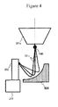
- Figure 4 shows a case where an electrode included in the electrode unit 204 is a parabola-shaped (paraboloidal surface shape) electrode 504.
- the figure indicates that it is possible to suppress expansion of irradiation position of the ion beam 301c by using the parabola-shaped electrode 504.
- an electrode in which electrodes with shapes shown in Figures 2 , 3 , and 4 are combined is used, it is possible to achieve various irradiation positions and irradiation angles by changing the location, inclination angle, and rotation angle of the electrode. In addition, it is also possible to change irradiation positions and irradiation angles by modulating the voltage applied to the electrode. In other words, it is possible to irradiate ion beams onto desired locations with desired angles by combining electrode shape, electrode voltage, electrode position, irradiation direction of ion beam, and sample movement.
- irradiate ion beams across the surface of sample 202 by changing the angle between the ion beam 301c and the extended line of the center axis of the ion beam column 201a using the electrode unit 204, and by moving the electrode unit 204 from side to side and up and down with the changed beam angle being kept.
- an electrode 604a spherical electrode
- an electrode 604b planar electrode
- the electrode unit 204 can be supported in any manner.
- an electrode supporting unit may be additionally provided, or the electrode can be attached instead of the micro sampling probe.
- the micro sampling probe itself can be an alternative of the electrode.
- the electrode unit 204 can be supported on one of the sample stages 219.
- the electrode unit 204 for bending trajectories of ions can be supported by the eucentric stage and the sample can be supported by the (S)TEM common sample holder.
- the electrode controller 211 can be configured to control the operations of the stage supporting the electrode unit 204.
- a polyhedral electrode can be applied as an example of above-mentioned electrodes.
- the processing result When processing a sample with heavy element and light element being mixed using ion beams, the processing result will be uneven due to the difference of sputtering rate, thus threads are formed in cross sections. For example, in a portion where heavy element and light element are present alternately in upper portions of the sample, the sputtering rate for such a portion will be decreased and threads will be formed in processing cross sections. This thread can be removed or decreased by arbitrarily changing irradiation direction of ion beams so that the sputtering rate will be even.
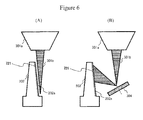
- Figure 6(A) shows a method for removing damaged layers where the present invention is not employed. If the surface 202a of the sample 202 is processed using an ion beam 301b, a damaged layer 721 is formed in the sample 202. The ion beam 301b used for removing the damaged layer 721 is irradiated from the same direction as the main processing beam. Therefore, as shown in Figure 6(A) , a very small portion of the ion beam 301b (a portion of side portion of the ion beam 301b) is used for removing the damaged layer 721. Thus it is very ineffective.
- the surface 202a of the sample 202 is processed using the ion beam 301b with the planar electrode 304 being moved from the shown location.
- the sample 202 is moved and the planar electrode 304 is moved to the shown location, thereby bending the ion beam 301b using the planar electrode 304 to irradiate the damaged layer 721.
- the ion beam 301b can be utilized with small loss to remove the damaged layer 721 efficiently.
- the location and inclination of the electrode 304 may be adjusted.
- Patent Literature 4 a method for obtaining vertical processing cross sections is employed in which a sample is inclined and then ion beams are irradiated.
- the irradiation directions of ion beams can be arbitrarily selected, it is possible to obtain vertical processing cross sections without inclining samples.
- the present invention is significantly beneficial in terms of observation in that ion beams can be irradiated from any direction.
- ion beams can be irradiated from any direction.
- an electrode can be used as a detector in obtaining SIM images.
- the electric current arriving at the electrode 204 is measured using the ammeter 207, and the measured electric current signal is provided to the integration computer 213 through the ammeter controller 218.
- the integration computer 213 obtains SIM images according to the electric current signal provided from the ammeter controller 218. Therefore, SIM images can be obtained even if the electrode 204 is placed near the sample 202.
- the electrode 204 with a negative charge applied to it is placed near the sample 202, the same thing can be said for secondary ions emitted from the sample 202.
- the travel distance of ion beams can be extended by irradiating ion beams onto the sample 202 in bypassing manner.
- the scannable range of ion beams depends on the distance from the emitted point of the ion beam column 201a and the sample 202. As the distance becomes longer, the observed region becomes wider.
- the scan range of focused ion beams can be expanded.
- observable range with low magnification can be expanded. This is beneficial in searching field of views. Further, it can be utilized when wider range is desired to be processed.
- the electrode 204 such as the electrode 304, 404, 504 is placed in the sample chamber 203, the electrode 204 being capable of adjusting its location in the direction along the extended line of the center axis of the ion beam column 201 a, the location in the direction perpendicular to the extended line, and the inclination angle ⁇ (the inclination angle with respect to the surface perpendicular to the extended line of the center axis of the ion beam column 201a).
- the ion beam 301c bended by the electrode 304 and the like is irradiated onto the surface of sample 202.
- an apparatus that can efficiently remove damaged layers and surface roughness that are formed on the surface irradiated by ion beams in FIB processing can be provided.
- the distance between the point where ion beams are emitted from the ion beam column 201 a and the sample surface can be extended. Therefore, the scan range can be expanded, thus the observed range with low magnification can be expanded.
- Figure 7 is a schematic overall configuration diagram of a charged particle beam apparatus according to an example 2 of the present invention.
- the charged particle beam apparatus in the example 2 comprises: a SEM column 807a; and an electron beam scan controller 818 for controlling a scan of an electron beam 807b of the SEM column 807a.
- Other configurations are the same as the example 1.
- the SEM column 807a is a system that includes all configurations necessary for SEM, such as an electron source for generating electron beams, a lens for focusing the electron beam, and a deflection system for scanning and shifting electron beams.
- the charged particle beam apparatus according to the example 2 of the present invention is an apparatus that can SEM-observe cross sections of the sample 202 processed by FIB on site.
- the ion beam column 201a is placed vertically and the SEM column 807a is placed with inclination.
- the ion beam column 201a can be placed with inclination and the SEM column 807a can be placed vertically.
- both of the ion beam column 201a and the SEM column 807a can be placed with inclinations.
- the charged particle beam device may have a triple column configuration with a Ga focused ion beam column, an Ar focused ion beam column, and an electron beam column.
- the detector for obtaining SEM images the detector controller that provides the integration computer with the detected information, and the display that displays SEM images generated from the detection signals are the same as those for SIM images.
- the charged particle beam apparatus may have one or more than one of detectors, detector controllers, and displays as the mechanism for obtaining and displaying SEM images.
- the processing state of the ion beam 201b can be SEM-observed from various directions by irradiating electrons with bended trajectories onto the sample 202.
- the processing state can be SEM-observed by irradiating the electron beam 807b from the SEM column 807a onto the front surface of the sample 202, as shown in Figure 7 .
- a parabola-shaped electrode 904 is placed so that the trajectory of the electron beam 807c from the SEM column 807a is bended to the sample 202 placed at the location where the ion beam 301c emitted from the tip 301a of the ion beam column 201a is irradiated. According to this, the back side 923 of the sample 202 viewed from the SEM column 807a can be observed. Therefore, the processing state can be identified at both sides of the thin film sample 202, thus sample processing accuracy can be improved.
- the acceleration voltage of the ion beam 301c is preferably set higher than the acceleration voltage of the electron beam 807c. That can achieve the electron trajectory as shown in Figure 8 with very small influence on the ion beam 301c.
- the acceleration voltage of the ion beam 807c is preferably set higher than the acceleration voltage of the electron beam 201b. That can achieve SEM observation with very small influence on the electron beam 807b.
- the travel distance of the electron beam 807b can be extended by irradiating the electron beam 807b onto the sample 202 in bypassing manner. This enables to expand the observable range with low magnification in SEM observation, as in the case of SIM observation.
- the same advantageous effect as that of the example 1 can be achieved.
- desired locations of the sample surface during processing by ion beams can be observed by SEM.
- electric fields are used for changing the trajectories of charged particles.
- magnetic fields also can be used for changing the trajectories of charged particles.
- the trajectories of charged particles can be changed by placing coils or permanent magnets in the sample chamber.
- thin film samples of state-of-the-art devices or functional materials can be produced with high quality, processing efficiency improves significantly, and analyzing accuracy in (S)TEM improves significantly.
- the FIB-SEM apparatus provides an apparatus that can SEM-observe the front surface of the sample as well as the back surface. In producing thin film samples, the both sides can be observed without moving the sample, thus processing accuracy and processing reproducibility improves significantly.
- 201a ion beam column, 201b, 301b, 301c: ion beam, 202: sample, 202a: sample surface, 203: sample chamber, 204: electrode unit, 205: electric voltage supplying device, 206: detector, 207: ammeter, 211: electrode controller, 212: electric voltage controller, 213: integration computer, 214: ion beam scan controller, 215: detector controller, 216: controller, 217: display, 218: ammeter controller, 219: sample stage, 721: damaged layer, 301a: ion beam column tip, 304, 604b: planar electrode, 404, 604a: spherical electrode, 504, 904: parabola electrode, 807a: scanning electron microscope column, 807b: electron beam, 807c: electron beam, 818: electron beam scan controller, 923: sample back surface
Landscapes
- Chemical & Material Sciences (AREA)
- Analytical Chemistry (AREA)
- Analysing Materials By The Use Of Radiation (AREA)
- Sampling And Sample Adjustment (AREA)
Abstract
In order to provide a charged particle beam apparatus capable of irradiating a desired region in the surface of a sample with a charged particle beam from a wide range of angles, an electrode unit (204) comprising an electrode, the inclination angle of which (i.e. the angle of inclination relative to a plane orthogonal to the extension line of the center axis of the ion beam column (201a)) and the position of which (i.e. the position in the direction along the extension line of the center axis of the ion beam column (201a) and in directions orthogonal thereto) can be adjusted, is arranged within a sample chamber (203) of the charged particle beam apparatus. The charged particle beam apparatus is also configured so that a curved ion beam (201b) is irradiated onto a surface of a sample (202) by the electrode. This enables irradiation of the ion beam (201b) to a desired range within the surface of the sample (202), from a wide range of angles with respect to the sample surface.
Description
- The present invention relates to, for example, a charged particle beam apparatus and a method of irradiating charged particle beam.
- In recent years, focused ion beam (FIB) apparatuses are used for producing thin film samples for observation of (scanning) transmission electron microscope ((S)TEM). Specifically, in producing thin film samples for analyzing defects of semiconductor devices, FIB apparatus is a necessary tool.
- In recent years, structural objects are being miniaturized in various industries such as the energy industry like fuel cell or solar cell and the industries using organic materials like organic electro-luminescence (EL) displays, with the semiconductor industry at the top of list. Improving processing techniques for observation samples and analysis samples is thus needed. For example, devices with node size of 30 nm or less are being applied in state of the art devices. In producing thin film samples of such devices for (S)TEM, nanometer-order processing accuracy is required. In addition, as structural objects become miniaturized and complicated, roughness of process cross-section (curtaining pattern) due to mixed light elements and heavy elements becomes a larger issue for (S)TEM observation samples. Therefore, in finally finishing (S)TEM observation thin film samples, it is required to accurately remove damaged layers and curtaining patterns in desired regions.
- In order to solve the problem above,
Patent Literature 1 indicates a method of using, for removing damaged layers, a second ion beam (argon ion) that is different from a first ion beam (gallium ion) used for thin film processing. - In addition, Patent Literature 2 indicates a method for removing damaged layers by irradiating an argon ion onto a film sample piece using an ion milling apparatus.
- In addition, Patent Literature 3 describes a method for decreasing damaged layers wherein energy of an ion beam used for finish processing is made lower than energy of an ion beam used for main processing. Further, it is also indicated that decrease in throughput can be suppressed by finish-processing the sample being inclined with respect to the ion beams.
- In addition, as a problem other than damaged layers, vertical cross-sections cannot be obtained by irradiating focused ion beams vertically with respect to the surface of samples. This is because the shape of focused ion beams is focused at the focused location. Thus a thin film sample is not appropriate as that for (S)TEM observation if it doesn't have a cross section that is vertical with respect to the surface of sample.
- As a method for preventing this problem, Patent Literature 4 indicates a method for obtaining a vertical cross section by irradiating an ion beam with a sample being inclined by a predetermined angle. The processing is generally performed with the surface of sample being inclined by 3 to 5 degree with respect to the center axis of ion beam.
- In addition, Patent Literature 5 describes a technique that can change the angle of ion beam with respect to the surface of sample from 75 degree to 90 degree using an angle changing electrode.
-
- Patent Literature 1:
JP Patent Publication (Kokai) No. 2004-264145 A - Patent Literature 2:
JP Patent Publication (Kokai) No. 2002-277364 A - Patent Literature 3:
JP Patent Publication (Kokai) No. 2007-193977 A - Patent Literature 4:
JP Patent Publication (Kokai) No. H08-5528 A (1996 - Patent Literature 5:
JP Patent Publication (Kokai) No. 2002-148159 A - However, in techniques described in
Patent Literatures 1 to 3, there is a significant restriction in irradiation direction of ion beam. Therefore, it is difficult to irradiate ion beams onto desired regions of sample only and to irradiate ion beams with optimal angle. - As the technique described in Patent Literature 4, in a technique where samples are inclined with respect to ion beams, it is also difficult to irradiate ion beams with desired angles onto desired regions by sample inclination only.
- Furthermore, in the technique described in Patent Literature 5, the angle of ion beams with respect to sample surfaces can be changed. However, it is impossible to irradiate ion beams with angles more than it. Thus it is difficult to irradiate ion beams with desired angles onto desired regions.
- The objective of the present invention is to achieve a charged particle beam apparatus and a method of irradiating charged particle beam that can irradiate charged particle beams onto desired regions of sample surfaces with wide range of angles.
- A charged particle beam apparatus according to the present invention comprises: an ion beam column; a sample chamber with the ion beam column attached to it; a sample stage located in the sample chamber; an electrode unit that is located in the sample chamber and changes a trajectory of an ion beam so that the ion beam is irradiated onto a sample supported by the sample stage; and an electrode unit movement control unit that moves the electrode unit.
- The electrode unit can change a trajectory of the ion beam generated from the ion beam column by changing an angle between the ion beam and an extended line of a center axis of the ion beam column. Thus the ion beam can be irradiated onto samples supported by the sample stage.
- According to the present invention, it is possible to achieve a charged particle beam apparatus and a method of irradiating charged particle beam that can irradiate charged particle beams onto desired regions of sample surfaces with wide range of angles.
-
- [
Figure 1] Figure 1 is a schematic configuration diagram of a charged particle beam apparatus according to an example 1 of the present invention. - [
Figure 2] Figure 2 is a diagram showing an example of an ion beam trajectory in the example 1 of the present invention. - [
Figure 3] Figure 3 is a diagram showing another example of an ion beam trajectory in the example 1 of the present invention. - [
Figure 4] Figure 4 is a diagram explaining another example of an ion beam trajectory in the example 1 of the present invention. - [
Figure 5] Figure 5 is a diagram showing another example of an ion beam trajectory in the example 1 of the present invention. - [
Figure 6] Figure 6 is a comparative explanation diagram between the method for removing damaged layer according to the example 1 of the present invention and another example of the present invention. - [
Figure 7] Figure 7 is a schematic configuration diagram of a charged particle beam apparatus according to an example 2 of the present invention. - [
Figure 8] Figure 8 is a diagram showing an example of an ion beam trajectory in the example 2 of the present invention. - In the present invention, an electrode unit for bending a trajectory of a charged particle is provided in a sample chamber of a charged particle beam apparatus comprising an ion beam column. The charged particle beams are bended by an electric field generated by the electrode unit to be irradiated onto a sample.
- Hereinafter, embodiments of the present invention will be described with reference to attached drawings. However, the embodiments described below are merely examples for implementing the present invention, and it is not intended to limit the technical scope of the present invention.
-
Figure 1 is a schematic overall configuration diagram of a charged particle beam apparatus according to an example 1 of the present invention. - In
Figure 1 , the charged particle beam apparatus comprises: an ion beam column 201a; asample chamber 203; anelectrode unit 204 that is provided in thesample chamber 203, is capable of being applied of electric voltages, is movable in any direction, and is capable of adjusting its inclination angle; anelectrode controller 211 that controls a location and an angle of theelectrode unit 204; an electricvoltage supplying device 205 for applying an electric voltage to theelectrode unit 204; anelectric voltage controller 212 that controls the electricvoltage supplying device 205; and anintegration computer 213 that controls overall operations of the charged particle beam apparatus. - The charged particle beam apparatus further comprises: an ion
beam scan controller 214 for controlling a scan of an ion beam 201b generated from the ion beam column 201a; adetector 206 for obtaining a scanning ion microscope (SIM) image; adetector controller 215 that provides theintegration computer 213 with the detected information; a controller (such as a keyboard, a mouse) 216 for operators to input various instructions such as irradiation conditions or electric voltage conditions and location conditions of electrodes; and adisplay 217 that displays the obtained SIM images. - The charged particle beam apparatus further comprises: an
ammeter 207 for using theelectrode unit 204 as a second detector; and anammeter controller 218 that performs processing such as amplifying electric current values detected by theammeter 207. An electric current measuring signal from theammeter controller 218 is provided to theintegration computer 213. - The ion beam column 201a is a system that includes all configurations necessary for FIB, such as an ion source for generating the ion beam 201b, a lens for focusing the ion beam 201b, a deflection system for scanning and shifting ion beams. The ion beam column 201a is equipped in the
sample chamber 203. Gallium ion is typically used for the ion beam 201b. However, any ion species can be used for the purpose of processing. - The ion beam 201b is not limited to focused ion beams and it can be a broad ion beam. In the example 1 of the present invention, a FIB column 201 a is provided. However, two or more than two of ion beam columns can be provided. For example, a configuration with a Ga focused ion beam column and an Ar focused ion beam column may be allowed.
- The electric
voltage supplying device 205 supplying electric voltages to theelectrode unit 204 can be modulated. Each of controllers can communicate with each other, and is controlled by theintegration computer 213. - In the example 1, a
detector 206 for obtaining SIM images is provided. However, a configuration with two or more than two of same or different detectors may be allowed. For example, a secondary electron detector and a secondary ion detector may be equipped. - Other than above-mentioned configurations, a sample stage, a gas deposition unit, a micro sampling unit, and the like are equipped in the
sample chamber 203. Asample 202 can be placed on a sample stage 219 (shown inFigure 2 ) for carrying samples. Thesample stage 219 can perform in-plane movement, rotation, and inclination. Thesample stage 219 can also move portions required for ion beam processing or observation to positions where ion beams are irradiated. - Other than semiconductor materials, iron and steel, light metal, polymer molecule, and the like can be expected as the
sample 202. The gas deposition unit that is used for producing protection films or markings stores deposition gases that form deposition films by irradiating charged particle beams, and can provide the gases from a nozzle tip as required. - The micro sampling unit picks up specific portions of the
sample 202 by using with processing or cutting of thesample 202 by FIB. The micro sampling unit includes a probe that can be moved in thesample chamber 203 by a probe driving unit. The probe is utilized for picking out small sample pieces formed in thesample 202 and for contacting with the sample surface to provide electric potentials to the sample. - The
detector controller 215 may comprise a circuit or a processing unit that processes a detection signal from thedetector 206 for imaging it. Each of driving mechanisms such as the sample stage, the deposition unit, and the micro sampling unit has control circuits respectively. Those control circuits can communicate with each other and are controlled by one or a plurality of computers in integrated manner. -
Figure 2 ,Figure 3 , andFigure 4 are magnified diagrams around thesample 202 shown inFigure 1 . -
Figure 2 shows a case where an electrode included in theelectrode unit 204 is aplanar electrode 304. It shows that anion beam 301c from atip 301a of the ion beam column 201a is bended and is irradiated onto thesample 202 supported by thesample stage 219. In this case, it is possible to change the irradiation position and the irradiation angle of theion beam 301c on thesample 202 by changing the location (the location in the direction along the extended line of the center axis of the ion beam column 201a, the location in the direction perpendicular to the extended line of the center axis of the ion beam column 201a) and the inclination angle α (the inclination angle with respect to the surface perpendicular to the extended line of the center axis of the ion beam column 201a) of theplanar electrode 304.Figure 2(A) shows a case where the inclination angle is αA andFigure 2(B) shows a case where the inclination angle is αB. -
Figure 3 shows a case where an electrode included in theelectrode unit 204 is aspherical electrode 404. In this case, it is possible to change the irradiation position and the irradiation angle of the ion beam on thesample 202 by horizontally moving the spherical electrode 404 (move in the direction perpendicular to the extended line of the center axis of the ion beam column 201a).Figure 3(A) is a case where the distance between the extended line of the center axis of the ion beam column 20 1 a and the center of thespherical electrode 404 is LA.Figure 3(B) is a case where the distance between the extended line of the center axis of the ion beam column 201a and the center of thespherical electrode 404 is LB. LA is larger than LB. -
Figure 4 shows a case where an electrode included in theelectrode unit 204 is a parabola-shaped (paraboloidal surface shape)electrode 504. The figure indicates that it is possible to suppress expansion of irradiation position of theion beam 301c by using the parabola-shapedelectrode 504. - If an electrode in which electrodes with shapes shown in
Figures 2 ,3 , and4 are combined is used, it is possible to achieve various irradiation positions and irradiation angles by changing the location, inclination angle, and rotation angle of the electrode. In addition, it is also possible to change irradiation positions and irradiation angles by modulating the voltage applied to the electrode. In other words, it is possible to irradiate ion beams onto desired locations with desired angles by combining electrode shape, electrode voltage, electrode position, irradiation direction of ion beam, and sample movement. Specifically, it is possible to irradiate ion beams onto sample surfaces with wide range of angles by changing the angle of theplanar electrode 304 from being perpendicular to the extended line of the center axis of the ion beam column 201a to being horizontal. - Alternatively, it is possible to irradiate ion beams across the surface of
sample 202 by changing the angle between theion beam 301c and the extended line of the center axis of the ion beam column 201a using theelectrode unit 204, and by moving theelectrode unit 204 from side to side and up and down with the changed beam angle being kept. - In addition, as shown in
Figure 5 , it is also possible to achieve desired irradiation locations and irradiation angles of thesample 202 by using a plurality of an electrode 604a (spherical electrode), anelectrode 604b (planar electrode) simultaneously. For example, it is possible to place thespherical electrode 604a (a first electrode unit) near thetip 301a of the ion beam column 201a and to place theplanar electrode 604b (a second electrode unit) near thesample 202. - For the purpose of bending the trajectory of the
ion beam 301c, theelectrode unit 204 can be supported in any manner. For example, an electrode supporting unit may be additionally provided, or the electrode can be attached instead of the micro sampling probe. Of course, the micro sampling probe itself can be an alternative of the electrode. In a case where a plurality of the sample stages 219 is provided, theelectrode unit 204 can be supported on one of the sample stages 219. For example, in a charged particle beam apparatus comprising: a sample stage with a XYZ driving mechanism, an inclination mechanism, and a rotation mechanism (eucentric stage); and a (S)TEM common sample holder, theelectrode unit 204 for bending trajectories of ions can be supported by the eucentric stage and the sample can be supported by the (S)TEM common sample holder. In this case, theelectrode controller 211 can be configured to control the operations of the stage supporting theelectrode unit 204. - In addition, other than planar electrode, spherical electrode, and parabola-shaped electrode, a polyhedral electrode can be applied as an example of above-mentioned electrodes.
- It is possible to irradiate ion beams from any direction by equipping, in a sample chamber, an electrode for bending ion trajectories in a charged particle beam apparatus having above-mentioned configurations and being capable of irradiating ion beams. Hereinafter, an explanation for such effects will be provided.
- When processing a sample with heavy element and light element being mixed using ion beams, the processing result will be uneven due to the difference of sputtering rate, thus threads are formed in cross sections. For example, in a portion where heavy element and light element are present alternately in upper portions of the sample, the sputtering rate for such a portion will be decreased and threads will be formed in processing cross sections. This thread can be removed or decreased by arbitrarily changing irradiation direction of ion beams so that the sputtering rate will be even.
- In addition, in producing thin film samples for (S)TEM, it is possible to prevent surface unevenness in observed regions by employing irradiation direction of ion beams such that the heavy element region is placed under the observed regions of the sample.
- According to the example 1 of the present invention, it is possible to irradiate ion beams from such irradiation directions.
- In addition, it is possible to remove damaged layers due to irradiation of ion beams efficiently.
-
Figure 6(A) shows a method for removing damaged layers where the present invention is not employed. If thesurface 202a of thesample 202 is processed using anion beam 301b, a damagedlayer 721 is formed in thesample 202. Theion beam 301b used for removing the damagedlayer 721 is irradiated from the same direction as the main processing beam. Therefore, as shown inFigure 6(A) , a very small portion of theion beam 301b (a portion of side portion of theion beam 301b) is used for removing the damagedlayer 721. Thus it is very ineffective. - In contrast, in the example shown in
Figure 6(B) where the present invention is applied, thesurface 202a of thesample 202 is processed using theion beam 301b with theplanar electrode 304 being moved from the shown location. After that, thesample 202 is moved and theplanar electrode 304 is moved to the shown location, thereby bending theion beam 301b using theplanar electrode 304 to irradiate the damagedlayer 721. According to such operation, theion beam 301b can be utilized with small loss to remove the damagedlayer 721 efficiently. - In addition, it is also possible to remove surface unevenness by controlling the location and inclination of the
electrode 304 to irradiate thesample 202 at desired regions with desired angles. For example, it is possible to efficiently remove surface roughness generated by irradiating ion beams. At that time, in addition to the location and inclination of theelectrode 304, the location and inclination of thesample 202 may be adjusted. - In addition, in producing thin film samples for (S)TEM, as indicated in Patent Literature 4, a method for obtaining vertical processing cross sections is employed in which a sample is inclined and then ion beams are irradiated. However, if the irradiation directions of ion beams can be arbitrarily selected, it is possible to obtain vertical processing cross sections without inclining samples. Furthermore, it is possible to intensively remove thick portions of the thin film (skirt portion) efficiently by irradiating ion beams from the bottom.
- Furthermore, the present invention is significantly beneficial in terms of observation in that ion beams can be irradiated from any direction. For example, it is possible to obtain SIM images from various directions even for a sample stage without inclination mechanism and rotation mechanism. For example, it is possible to obtain SIM images observed from bottom of column or SIM images observed from horizontal directions with respect to the optical axis. As a result, it is possible to more precisely analyze the three-dimensional structure of samples. Note that an electrode can be used as a detector in obtaining SIM images.
- By the way, in
Figure 1 , if theelectrode 204 in which a positive voltage is applied is placed near thesample 202, most of secondary electrons emitted from thesample 202 are attracted by the electric voltage of theelectrode 204, thus cannot reach thedetector 206. Therefore, it is difficult for thedetector 206 to obtain SIM images. - Then, the electric current arriving at the
electrode 204 is measured using theammeter 207, and the measured electric current signal is provided to theintegration computer 213 through theammeter controller 218. Theintegration computer 213 obtains SIM images according to the electric current signal provided from theammeter controller 218. Therefore, SIM images can be obtained even if theelectrode 204 is placed near thesample 202. - If the
electrode 204 with a negative charge applied to it is placed near thesample 202, the same thing can be said for secondary ions emitted from thesample 202. - As such, it is possible to efficiently remove amorphous layers and roughness of observed surfaces that are formed by irradiating focused ion beams and to more precisely know how the sample is being processed.
- Next, a description will be provided explaining that observable ranges with low magnification can be expanded according to the example 1 of the present invention.
- As the example 1 of the present invention, the travel distance of ion beams can be extended by irradiating ion beams onto the
sample 202 in bypassing manner. The scannable range of ion beams depends on the distance from the emitted point of the ion beam column 201a and thesample 202. As the distance becomes longer, the observed region becomes wider. - Therefore, according to the example 1 of the present invention, the scan range of focused ion beams can be expanded. In other words, observable range with low magnification can be expanded. This is beneficial in searching field of views. Further, it can be utilized when wider range is desired to be processed.
- As discussed above, according to the example 1 of the present invention, the
electrode 204 such as theelectrode sample chamber 203, theelectrode 204 being capable of adjusting its location in the direction along the extended line of the center axis of the ion beam column 201 a, the location in the direction perpendicular to the extended line, and the inclination angle α (the inclination angle with respect to the surface perpendicular to the extended line of the center axis of the ion beam column 201a). Theion beam 301c bended by theelectrode 304 and the like is irradiated onto the surface ofsample 202. Thus a charged particle beam apparatus and a method of irradiating charged particle beam that can irradiate ion beams onto desired regions of sample surface inclined by any angle of wide range with respect to the sample surface can be achieved. - As discussed above, according to the example 1 of the present invention, an apparatus that can efficiently remove damaged layers and surface roughness that are formed on the surface irradiated by ion beams in FIB processing can be provided.
- Furthermore, the distance between the point where ion beams are emitted from the ion beam column 201 a and the sample surface can be extended. Therefore, the scan range can be expanded, thus the observed range with low magnification can be expanded.
-
Figure 7 is a schematic overall configuration diagram of a charged particle beam apparatus according to an example 2 of the present invention. - In addition to the apparatus configuration in the example 1, the charged particle beam apparatus in the example 2 comprises: a
SEM column 807a; and an electronbeam scan controller 818 for controlling a scan of an electron beam 807b of theSEM column 807a. Other configurations are the same as the example 1. - The
SEM column 807a is a system that includes all configurations necessary for SEM, such as an electron source for generating electron beams, a lens for focusing the electron beam, and a deflection system for scanning and shifting electron beams. - The charged particle beam apparatus according to the example 2 of the present invention is an apparatus that can SEM-observe cross sections of the
sample 202 processed by FIB on site. - In the example 2 of the present invention, the ion beam column 201a is placed vertically and the
SEM column 807a is placed with inclination. However, they are not limited to such configurations. The ion beam column 201a can be placed with inclination and theSEM column 807a can be placed vertically. In addition, both of the ion beam column 201a and theSEM column 807a can be placed with inclinations. - The charged particle beam device may have a triple column configuration with a Ga focused ion beam column, an Ar focused ion beam column, and an electron beam column. In addition, in the example 2 of the present invention, the detector for obtaining SEM images, the detector controller that provides the integration computer with the detected information, and the display that displays SEM images generated from the detection signals are the same as those for SIM images. However, the charged particle beam apparatus may have one or more than one of detectors, detector controllers, and displays as the mechanism for obtaining and displaying SEM images.
- A description will be provided explaining SEM-observation of processing state in the example 2 of the present invention.
- In the example 2 of the present invention in which the charged particle beam apparatus comprises the
SEM column 807a, the processing state of the ion beam 201b can be SEM-observed from various directions by irradiating electrons with bended trajectories onto thesample 202. - When observing the front surface of the
sample 202, the processing state can be SEM-observed by irradiating the electron beam 807b from theSEM column 807a onto the front surface of thesample 202, as shown inFigure 7 . - In addition, as shown in
Figure 8 , a parabola-shapedelectrode 904 is placed so that the trajectory of theelectron beam 807c from theSEM column 807a is bended to thesample 202 placed at the location where theion beam 301c emitted from thetip 301a of the ion beam column 201a is irradiated. According to this, theback side 923 of thesample 202 viewed from theSEM column 807a can be observed. Therefore, the processing state can be identified at both sides of thethin film sample 202, thus sample processing accuracy can be improved. - When SEM-observing the sample back
side 923 viewed from theSEM column 807a during processing samples by irradiating the ion beam 201b, the acceleration voltage of theion beam 301c is preferably set higher than the acceleration voltage of theelectron beam 807c. That can achieve the electron trajectory as shown inFigure 8 with very small influence on theion beam 301c. - On the other hand, when SEM-observing during processing samples using the ion beam 201b with trajectories bended by the
electrode 204, the acceleration voltage of theion beam 807c is preferably set higher than the acceleration voltage of the electron beam 201b. That can achieve SEM observation with very small influence on the electron beam 807b. - In addition, the travel distance of the electron beam 807b can be extended by irradiating the electron beam 807b onto the
sample 202 in bypassing manner. This enables to expand the observable range with low magnification in SEM observation, as in the case of SIM observation. - According to the example 2 of the present invention, the same advantageous effect as that of the example 1 can be achieved. In addition, as described above, desired locations of the sample surface during processing by ion beams can be observed by SEM.
- Both in the example 1 and 2 of the present invention, electric fields are used for changing the trajectories of charged particles. However, magnetic fields also can be used for changing the trajectories of charged particles. For example, the trajectories of charged particles can be changed by placing coils or permanent magnets in the sample chamber.
- In addition, thin film samples of state-of-the-art devices or functional materials can be produced with high quality, processing efficiency improves significantly, and analyzing accuracy in (S)TEM improves significantly.
- Furthermore, the FIB-SEM apparatus provides an apparatus that can SEM-observe the front surface of the sample as well as the back surface. In producing thin film samples, the both sides can be observed without moving the sample, thus processing accuracy and processing reproducibility improves significantly.
- 201a: ion beam column, 201b, 301b, 301c: ion beam, 202: sample, 202a: sample surface, 203: sample chamber, 204: electrode unit, 205: electric voltage supplying device, 206: detector, 207: ammeter, 211: electrode controller, 212: electric voltage controller, 213: integration computer, 214: ion beam scan controller, 215: detector controller, 216: controller, 217: display, 218: ammeter controller, 219: sample stage, 721: damaged layer, 301a: ion beam column tip, 304, 604b: planar electrode, 404, 604a: spherical electrode, 504, 904: parabola electrode, 807a: scanning electron microscope column, 807b: electron beam, 807c: electron beam, 818: electron beam scan controller, 923: sample back surface
Claims (18)
- A charged particle beam apparatus comprising:an ion beam column irradiating an ion beam;a sample chamber with the ion beam column attached to it;a sample stage that is located in the sample chamber and supports a sample;an electrode unit that is located in the sample chamber and changes a trajectory of the ion beam generated from the ion beam column so that the ion beam is irradiated onto the sample supported by the sample stage;an electrode unit movement controller moving the electrode unit in the sample chamber; andan electric voltage supplying unit supplying an electric voltage to the electrode unit.
- The charged particle beam apparatus according to claim 1, wherein:the electrode unit movement controller controls a location of the electrode unit and an inclination angle of the electrode unit.
- The charged particle beam apparatus according to claim 2, wherein:the electrode unit is located below the sample supported by the sample stage viewed from the ion beam column so that the ion beam is irradiated onto the sample.
- The charged particle beam apparatus according to claim 2, wherein:the electrode unit includes a planar electrode.
- The charged particle beam apparatus according to claim 2, wherein:the electrode unit includes a spherical electrode.
- The charged particle beam apparatus according to claim 2, wherein:the electrode unit includes a paraboloid-shaped electrode.
- The charged particle beam apparatus according to claim 2, wherein:the electrode unit includes an polyhedral electrode.
- The charged particle beam apparatus according to claim 1, wherein:the electrode unit includes a first electrode unit placed near the ion beam column and a second electrode unit placed near the sample stage.
- The charged particle beam apparatus according to claim 1, further comprising:an electric current measuring unit detecting a secondary ion or a secondary electron arriving at the electrode unit; andan integration computer forming a scanning ion microscope image according to the secondary ion or the secondary electron measured by the electric current measuring unit.
- A charged particle beam apparatus comprising:an ion beam column irradiating an ion beam;a sample chamber with the ion beam column attached to it;a plurality of sample stages that are located in the sample chamber and support a sample;an electrode unit that is located in one of the plurality of sample stages located in the sample chamber and changes a trajectory of the ion beam generated from the ion beam column so that the ion beam is irradiated onto the sample supported by another one of the plurality of sample stages;an electrode unit movement controller moving the electrode unit in the sample chamber; andan electric voltage supplying unit supplying an electric voltage to the electrode unit.
- The charged particle beam apparatus according to claim 10, wherein:the electrode unit movement controller controls a location of the electrode unit and an inclination angle of the electrode unit.
- The charged particle beam apparatus according to claim 10, wherein:the electrode unit movement controller locates the electrode unit below the sample supported by the sample stage viewed from the ion beam column so that the ion beam is irradiated onto the sample.
- The charged particle beam apparatus according to claim 1, further comprising:a scanning electron microscope column irradiating an electron beam onto the sample supported by the sample stage or onto the electrode unit; andan electron beam scan controller controlling a scan of the electron beam irradiated from the scanning electron microscope column.
- A method of irradiating charged particle beam in a charged particle beam apparatus comprising an ion beam column irradiating an ion beam, a sample chamber with the ion beam column attached to it, and a sample stage that is located in the sample chamber and supports a sample, comprising:a step of changing a trajectory of the ion beam generated from the ion beam column by changing an angle between the ion beam and an extended line of a center axis of the ion beam column using a movable electrode unit that is placed in the sample chamber and is provided with an electric voltage, so that the ion beam is irradiated onto the sample supported by the sample stage.
- The method of irradiating charged particle beam according to claim 14, further comprising:a step of controlling a location of the electrode unit and an inclination angle of the electrode unit.
- The method of irradiating charged particle beam according to claim 15, wherein:the electrode unit movement controller locates the electrode unit below the sample supported by the sample stage viewed from the ion beam column so that the ion beam is irradiated onto the sample.
- The method of irradiating charged particle beam according to claim 15, wherein:an irradiation direction of the ion beam is changed using a first electrode unit placed near the ion beam column and a second electrode unit placed near the sample stage.
- The method of irradiating charged particle beam according to claim 14, wherein:a secondary ion or a secondary electron arriving at the electrode unit is detected by an electric current measuring unit, and a scanning ion microscope image is formed according to the secondary ion or the secondary electron measured by the electric current measuring unit.
Applications Claiming Priority (2)
| Application Number | Priority Date | Filing Date | Title |
|---|---|---|---|
| JP2010271806A JP5489295B2 (en) | 2010-12-06 | 2010-12-06 | Charged particle beam apparatus and charged particle beam irradiation method |
| PCT/JP2011/077670 WO2012077554A1 (en) | 2010-12-06 | 2011-11-30 | Charged particle beam apparatus and method of irradiating charged particle beam |
Publications (1)
| Publication Number | Publication Date |
|---|---|
| EP2650901A1 true EP2650901A1 (en) | 2013-10-16 |
Family
ID=46207044
Family Applications (1)
| Application Number | Title | Priority Date | Filing Date |
|---|---|---|---|
| EP11847394.1A Withdrawn EP2650901A1 (en) | 2010-12-06 | 2011-11-30 | Charged particle beam apparatus and method of irradiating charged particle beam |
Country Status (4)
| Country | Link |
|---|---|
| US (1) | US20130248733A1 (en) |
| EP (1) | EP2650901A1 (en) |
| JP (1) | JP5489295B2 (en) |
| WO (1) | WO2012077554A1 (en) |
Families Citing this family (3)
| Publication number | Priority date | Publication date | Assignee | Title |
|---|---|---|---|---|
| JP6108674B2 (en) * | 2012-03-16 | 2017-04-05 | 株式会社日立ハイテクサイエンス | Charged particle beam apparatus and sample transport apparatus |
| WO2014184881A1 (en) * | 2013-05-14 | 2014-11-20 | 株式会社日立製作所 | Sample holder and focused-ion-beam machining device provided therewith |
| US10388489B2 (en) | 2017-02-07 | 2019-08-20 | Kla-Tencor Corporation | Electron source architecture for a scanning electron microscopy system |
Family Cites Families (18)
| Publication number | Priority date | Publication date | Assignee | Title |
|---|---|---|---|---|
| US4096386A (en) * | 1977-04-04 | 1978-06-20 | Taylor-Kincaid Company | Light reflecting electrostatic electron lens |
| DE3525994A1 (en) * | 1985-07-20 | 1987-01-29 | Philips Patentverwaltung | ELECTRON BEAM RECORDING CARRIER |
| JPH0734871B2 (en) * | 1989-09-14 | 1995-04-19 | 株式会社クボタ | Rice mill |
| JPH03101849U (en) * | 1990-02-02 | 1991-10-23 | ||
| JP3058394B2 (en) | 1994-06-23 | 2000-07-04 | シャープ株式会社 | Preparation method for cross-section specimen for transmission electron microscope |
| US6521895B1 (en) * | 1999-10-22 | 2003-02-18 | Varian Semiconductor Equipment Associates, Inc. | Wide dynamic range ion beam scanners |
| DE10010523C2 (en) * | 2000-03-07 | 2002-08-14 | Schwerionenforsch Gmbh | Ion beam system for the irradiation of tumor tissue |
| JP2002117796A (en) * | 2000-10-11 | 2002-04-19 | Jeol Ltd | Charged particle beam device and focused ion beam device |
| JP4283432B2 (en) | 2000-11-06 | 2009-06-24 | 株式会社日立製作所 | Sample preparation equipment |
| JP2002277364A (en) | 2001-03-19 | 2002-09-25 | Seiko Epson Corp | Thin sample processing method and thin sample preparation method |
| JP3768197B2 (en) | 2003-02-28 | 2006-04-19 | 株式会社東芝 | Preparation method of transmission electron microscope specimen |
| JP4128487B2 (en) * | 2003-06-02 | 2008-07-30 | 株式会社日立ハイテクノロジーズ | Charged particle beam equipment |
| JP2006032154A (en) * | 2004-07-16 | 2006-02-02 | Hiroyuki Noguchi | Focusing ion beam working method and focusing ion beam working device |
| JP2007012516A (en) * | 2005-07-01 | 2007-01-18 | Jeol Ltd | Charged particle beam apparatus and sample information detection method using charged particle beam |
| JP5142240B2 (en) | 2006-01-17 | 2013-02-13 | 株式会社日立ハイテクノロジーズ | Charged beam apparatus and charged beam processing method |
| JP5016988B2 (en) * | 2007-06-19 | 2012-09-05 | 株式会社日立ハイテクノロジーズ | Charged particle beam apparatus and vacuum startup method thereof |
| JP4901696B2 (en) * | 2007-11-06 | 2012-03-21 | キヤノンアネルバ株式会社 | Deposition equipment |
| JP2011146690A (en) * | 2009-12-18 | 2011-07-28 | Canon Anelva Corp | Ion beam generator and substrate processing apparatus and production method of electronic device using the ion beam generator |
-
2010
- 2010-12-06 JP JP2010271806A patent/JP5489295B2/en not_active Expired - Fee Related
-
2011
- 2011-11-30 WO PCT/JP2011/077670 patent/WO2012077554A1/en not_active Ceased
- 2011-11-30 US US13/991,678 patent/US20130248733A1/en not_active Abandoned
- 2011-11-30 EP EP11847394.1A patent/EP2650901A1/en not_active Withdrawn
Non-Patent Citations (1)
| Title |
|---|
| See references of WO2012077554A1 * |
Also Published As
| Publication number | Publication date |
|---|---|
| JP2012123942A (en) | 2012-06-28 |
| JP5489295B2 (en) | 2014-05-14 |
| US20130248733A1 (en) | 2013-09-26 |
| WO2012077554A1 (en) | 2012-06-14 |
Similar Documents
| Publication | Publication Date | Title |
|---|---|---|
| CN104241066B (en) | Method for imaging a sample in a charged particle apparatus | |
| US10522327B2 (en) | Method of operating a charged particle beam specimen inspection system | |
| KR102579329B1 (en) | CAD-assisted TEM prep recipe creation | |
| US9177760B2 (en) | TEM sample preparation | |
| JP5292348B2 (en) | Compound charged particle beam system | |
| US9281163B2 (en) | High capacity TEM grid | |
| TWI813760B (en) | Sample Processing Observation Method | |
| US20090166557A1 (en) | Charge control apparatus and measurement apparatus equipped with the charge control apparatus | |
| KR102590634B1 (en) | Charged particle beam apparatus and sample processing method | |
| CN104251795B (en) | Plan view sample preparation | |
| US10600612B2 (en) | Charged particle beam apparatus | |
| US20140092230A1 (en) | Method for avoiding artefacts during serial block face imaging | |
| CN109841534A (en) | Section processes observation method, charged particle beam apparatus | |
| KR102641280B1 (en) | Method for measuring critical dimensions on a substrate, and apparatus for inspecting and cutting electronic devices on the substrate | |
| KR20150077234A (en) | Scanning Electron Microscope | |
| US20130248733A1 (en) | Charged particle beam apparatus and method of irradiating charged particle beam | |
| JP2016066553A (en) | Charged particle beam equipment | |
| US20200300736A1 (en) | Thin-sample-piece fabricating device and thin-sample-piece fabricating method | |
| JP4520905B2 (en) | Analysis device, probe control method, and analysis system | |
| US20240055220A1 (en) | Charged Particle Beam Device | |
| JP2013105603A (en) | Charged particle beam device |
Legal Events
| Date | Code | Title | Description |
|---|---|---|---|
| PUAI | Public reference made under article 153(3) epc to a published international application that has entered the european phase |
Free format text: ORIGINAL CODE: 0009012 |
|
| 17P | Request for examination filed |
Effective date: 20130708 |
|
| AK | Designated contracting states |
Kind code of ref document: A1 Designated state(s): AL AT BE BG CH CY CZ DE DK EE ES FI FR GB GR HR HU IE IS IT LI LT LU LV MC MK MT NL NO PL PT RO RS SE SI SK SM TR |
|
| DAX | Request for extension of the european patent (deleted) | ||
| STAA | Information on the status of an ep patent application or granted ep patent |
Free format text: STATUS: THE APPLICATION HAS BEEN WITHDRAWN |
|
| 18W | Application withdrawn |
Effective date: 20141118 |