EP2649518B1 - Programmierbarer atomarer speicher mit gespeicherten atomaren verfahren - Google Patents
Programmierbarer atomarer speicher mit gespeicherten atomaren verfahren Download PDFInfo
- Publication number
- EP2649518B1 EP2649518B1 EP11808979.6A EP11808979A EP2649518B1 EP 2649518 B1 EP2649518 B1 EP 2649518B1 EP 11808979 A EP11808979 A EP 11808979A EP 2649518 B1 EP2649518 B1 EP 2649518B1
- Authority
- EP
- European Patent Office
- Prior art keywords
- sequence
- instruction
- atomic
- instructions
- processing core
- Prior art date
- Legal status (The legal status is an assumption and is not a legal conclusion. Google has not performed a legal analysis and makes no representation as to the accuracy of the status listed.)
- Active
Links
- 230000015654 memory Effects 0.000 title claims description 92
- 238000000034 method Methods 0.000 title claims description 33
- 238000012545 processing Methods 0.000 claims description 85
- 238000010200 validation analysis Methods 0.000 claims description 67
- 230000004044 response Effects 0.000 claims description 15
- 238000012986 modification Methods 0.000 claims description 3
- 230000004048 modification Effects 0.000 claims description 3
- 238000012419 revalidation Methods 0.000 claims 1
- 238000010586 diagram Methods 0.000 description 16
- 230000007246 mechanism Effects 0.000 description 8
- 230000002093 peripheral effect Effects 0.000 description 5
- 230000015572 biosynthetic process Effects 0.000 description 3
- 238000004519 manufacturing process Methods 0.000 description 3
- 238000013507 mapping Methods 0.000 description 3
- 230000003287 optical effect Effects 0.000 description 3
- 239000000523 sample Substances 0.000 description 3
- 239000004065 semiconductor Substances 0.000 description 3
- 238000003786 synthesis reaction Methods 0.000 description 3
- 230000015556 catabolic process Effects 0.000 description 2
- 238000006731 degradation reaction Methods 0.000 description 2
- 230000006870 function Effects 0.000 description 2
- 230000009191 jumping Effects 0.000 description 2
- ZICZZIRIRHGROF-UHFFFAOYSA-N 1-$l^{1}-oxidanyl-2,2,4,5,5-pentamethylimidazole Chemical compound CC1=NC(C)(C)N([O])C1(C)C ZICZZIRIRHGROF-UHFFFAOYSA-N 0.000 description 1
- 101100078188 Saccharomyces cerevisiae (strain ATCC 204508 / S288c) MST27 gene Proteins 0.000 description 1
- 206010000210 abortion Diseases 0.000 description 1
- 230000002411 adverse Effects 0.000 description 1
- 238000013459 approach Methods 0.000 description 1
- 230000001174 ascending effect Effects 0.000 description 1
- 230000003190 augmentative effect Effects 0.000 description 1
- 230000006399 behavior Effects 0.000 description 1
- 230000003542 behavioural effect Effects 0.000 description 1
- 230000008901 benefit Effects 0.000 description 1
- 238000004891 communication Methods 0.000 description 1
- 238000010276 construction Methods 0.000 description 1
- 238000013461 design Methods 0.000 description 1
- 230000000694 effects Effects 0.000 description 1
- 230000009249 intrinsic sympathomimetic activity Effects 0.000 description 1
- 238000001693 membrane extraction with a sorbent interface Methods 0.000 description 1
- 230000002085 persistent effect Effects 0.000 description 1
- 230000008569 process Effects 0.000 description 1
- 239000007787 solid Substances 0.000 description 1
- 230000002123 temporal effect Effects 0.000 description 1
- 238000012360 testing method Methods 0.000 description 1
- 238000012546 transfer Methods 0.000 description 1
Images


Classifications
-
- G—PHYSICS
- G06—COMPUTING; CALCULATING OR COUNTING
- G06F—ELECTRIC DIGITAL DATA PROCESSING
- G06F9/00—Arrangements for program control, e.g. control units
- G06F9/06—Arrangements for program control, e.g. control units using stored programs, i.e. using an internal store of processing equipment to receive or retain programs
- G06F9/30—Arrangements for executing machine instructions, e.g. instruction decode
- G06F9/38—Concurrent instruction execution, e.g. pipeline, look ahead
-
- G—PHYSICS
- G06—COMPUTING; CALCULATING OR COUNTING
- G06F—ELECTRIC DIGITAL DATA PROCESSING
- G06F9/00—Arrangements for program control, e.g. control units
- G06F9/06—Arrangements for program control, e.g. control units using stored programs, i.e. using an internal store of processing equipment to receive or retain programs
- G06F9/30—Arrangements for executing machine instructions, e.g. instruction decode
- G06F9/30181—Instruction operation extension or modification
- G06F9/30189—Instruction operation extension or modification according to execution mode, e.g. mode flag
-
- G—PHYSICS
- G06—COMPUTING; CALCULATING OR COUNTING
- G06F—ELECTRIC DIGITAL DATA PROCESSING
- G06F9/00—Arrangements for program control, e.g. control units
- G06F9/06—Arrangements for program control, e.g. control units using stored programs, i.e. using an internal store of processing equipment to receive or retain programs
- G06F9/30—Arrangements for executing machine instructions, e.g. instruction decode
- G06F9/30003—Arrangements for executing specific machine instructions
- G06F9/3004—Arrangements for executing specific machine instructions to perform operations on memory
-
- G—PHYSICS
- G06—COMPUTING; CALCULATING OR COUNTING
- G06F—ELECTRIC DIGITAL DATA PROCESSING
- G06F9/00—Arrangements for program control, e.g. control units
- G06F9/06—Arrangements for program control, e.g. control units using stored programs, i.e. using an internal store of processing equipment to receive or retain programs
- G06F9/30—Arrangements for executing machine instructions, e.g. instruction decode
- G06F9/30003—Arrangements for executing specific machine instructions
- G06F9/30076—Arrangements for executing specific machine instructions to perform miscellaneous control operations, e.g. NOP
- G06F9/30087—Synchronisation or serialisation instructions
-
- G—PHYSICS
- G06—COMPUTING; CALCULATING OR COUNTING
- G06F—ELECTRIC DIGITAL DATA PROCESSING
- G06F9/00—Arrangements for program control, e.g. control units
- G06F9/06—Arrangements for program control, e.g. control units using stored programs, i.e. using an internal store of processing equipment to receive or retain programs
- G06F9/30—Arrangements for executing machine instructions, e.g. instruction decode
- G06F9/38—Concurrent instruction execution, e.g. pipeline, look ahead
- G06F9/3824—Operand accessing
- G06F9/3834—Maintaining memory consistency
-
- G—PHYSICS
- G06—COMPUTING; CALCULATING OR COUNTING
- G06F—ELECTRIC DIGITAL DATA PROCESSING
- G06F9/00—Arrangements for program control, e.g. control units
- G06F9/06—Arrangements for program control, e.g. control units using stored programs, i.e. using an internal store of processing equipment to receive or retain programs
- G06F9/46—Multiprogramming arrangements
- G06F9/466—Transaction processing
- G06F9/467—Transactional memory
Definitions
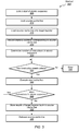
- the example instruction set above includes no instructions that access shared memory outside of the cache line where the program is encoded. Furthermore, the instruction set includes no jump instructions that might cause execution to be transferred to a location outside of the program. Therefore, any valid program encoded using the example instruction set meets at least the atomicity criteria forbidding access to shared memory and jumps to locations outside of the atomic sequence.
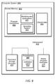
- FIG. 8 is a block diagram illustrating a computer system configured to execute an atomic sequence of instructions as a single atomic transaction using code validation agent, according to some examples, as described herein.
- computer system 800 may correspond to computer system 190 of FIG. 1 .
- Computer system 800 may also include one or more persistent storage devices 850 (e.g. optical storage, magnetic storage, hard drive, tape drive, solid state memory, etc.), which may persistently store data.
- persistent storage devices 850 e.g. optical storage, magnetic storage, hard drive, tape drive, solid state memory, etc.
Landscapes
- Engineering & Computer Science (AREA)
- Software Systems (AREA)
- Theoretical Computer Science (AREA)
- Physics & Mathematics (AREA)
- General Engineering & Computer Science (AREA)
- General Physics & Mathematics (AREA)
- Executing Machine-Instructions (AREA)
- Memory System Of A Hierarchy Structure (AREA)
Claims (15)
- Vorrichtung, umfassend:einen Prozessorkern (105) in einem Mehrkernprozessorsystem (100), wobei der Prozessorkern zu Folgendem ausgestaltet ist:zum Validieren, dass eine festgelegte Anweisungssequenz eine Gruppe eines oder mehrerer Atomaritätskriterien erfüllt, um eine validierte Anweisungssequenz zu produzieren, die dazu ausgestaltet ist, über ein oder mehrere Zielregister (110) auf Daten von einer oder mehreren Cachelinien zuzugreifen, wobei das eine oder mehrere Atomaritätskriterien ein Kriterium enthalten, dem zufolge keine Anweisung in der festgelegten Sequenz den Prozessorkern zum Zugriff auf geteilte Speicher anweist, ohne über das eine oder mehrere Zielregister zu laufen;zum Speichern der validierten Anweisungssequenz, wobei die gespeicherte validierte Anweisungssequenz als ein atomarer Speichervorgang ausführbar ist, ohne eine Neuvalidierung zu erfordern; undzum Aufrufen der gespeicherten validierten Sequenz zur Ausführung durch das Mehrkernprozessorsystem als ein atomarer Speichervorgang, wobei die Ausführung der validierten Anweisungssequenz als atomarer Speichervorgang das Speichern von Daten aus der einen oder mehreren Cachelinien in dem einen oder mehreren Zielregistern umfasst.
- Vorrichtung nach Anspruch 1, wobei der Prozessorkern zu Folgendem ausgestaltet ist, um die validierte Sequenz als atomarer Speichervorgang auszuführen:zum Ausführen der Anweisungssequenz, um die in dem einen oder mehreren Zielregistern gespeicherten Daten abzuändern; undzum Speichern eines oder mehrerer Werte aus dem einen oder mehreren Zielregistern in der einen oder mehreren Cachelinien.
- Vorrichtung nach Anspruch 2, wobei der Prozessorkern zum Ausführen des atomaren Speichervorgangs außerdem dazu ausgestaltet ist, die eine oder mehreren Cachelinien vor dem Speichern von Speicherdaten aus der einen oder mehreren Cachelinien in dem einen oder mehreren Zielregistern zu sperren und die eine oder mehreren Cachelinien nach dem Speichern des Wertes von dem einen oder mehreren Zielregister in eine oder mehrere Cachelinien zu entsperren, wobei das Sperren der einen oder mehreren Cachelinien den Prozessorkern dazu veranlasst, einen oder mehrere Prozessorkerne vom Lesen der geteilten Daten, die in der einen oder mehreren Cachelinien gespeichert sind, abzuhalten bzw. davon, diese Daten abzuändern, während die eine oder mehrere Cachelinien gesperrt sind.
- Vorrichtung nach Anspruch 2, wobei der validierten Anweisungssequenz eine Sonderzweck-Startanweisung vorausgeht, die darauf hinweist, dass die Sequenz als ein atomarer Speichervorgang auszuführen ist, wobei die Sonderzweck-Startanweisung auf die eine oder mehrere Cachelinien hinweist.
- Vorrichtung nach Anspruch 1, wobei der Prozessorkern zur Durchführung der Validierung mithilfe eines Mikroprogramm-Validierungsagenten (134) ausgestaltet ist.
- Vorrichtung nach Anspruch 5, wobei der Mikroprogramm-Validierungsagent zu Folgendem ausgestaltet ist:zum Empfangen eines Hinweises der Sequenz von einem Benutzerprogramm; undzur Durchführung der Validierung und des Speicherns in Reaktion auf das Empfangen des Hinweises der Sequenz.
- Vorrichtung nach Anspruch 6, wobei der Validierungsagent außerdem dazu ausgestaltet ist, dem Benutzerprogramm eine Kennung für die gespeicherte validierte Sequenz zurückzusenden, und wobei das Ausführen des atomaren Speichervorgangs in Reaktion auf die Benutzung der Kennung durch das Benutzerprogramm stattfindet, um die validierte Sequenz aufzurufen.
- Vorrichtung nach Anspruch 7, wobei das Benutzerprogramm auf die eine oder mehrere Cachelinien und das eine oder mehrere Zielregister hinweist.
- Vorrichtung nach Anspruch 1, wobei der Prozessorkern den atomaren Speichervorgang ausführt, ohne Unterbrechungen oder Seitenfehler zu erlauben.
- Vorrichtung nach Anspruch 1, wobei die Gruppe eines oder mehrerer Atomaritätskriterien eines oder mehrere der folgenden enthält: ein Kriterium, dem zufolge keine Anweisung in der Sequenz den Prozessorkern anweist, die Ausführung bei einer Anweisung außerhalb der Sequenz fortzusetzen, ein Kriterium, dem zufolge keine Anweisung in der Sequenz den Prozessorkern dazu anweist, auf ein anderes Register des Prozessorkerns als ein Allzweckregister zuzugreifen, ein Kriterium, dem zufolge jede Anweisung in der Sequenz in einem im Voraus festgelegten, begrenzten Längenformat ausgedrückt wird, ein Kriterium, dem zufolge keine Anweisung in der Sequenz den Prozessorkern zum Speicherzugriff anweist, sowie ein Kriterium, dem zufolge die Anzahl von Anweisungen in der Anweisungssequenz eine vorgegebene Obergrenze nicht überschreitet.
- Verfahren, umfassend:einen Prozessorkern (105) in einem Mehrkernprozessorsystem (100), der validiert, dasseine festgelegte Sequenz von Anweisungen eine Gruppe eines oder mehrerer Atomaritätskriterien erfüllt, um eine validierte Anweisungssequenz zu produzieren, die dazu ausgestaltet ist, über ein oder mehrere Zielregister (110) auf Daten von einer oder mehreren Cachelinien zuzugreifen, wobei das eine oder mehrere Atomaritätskriterien ein Kriterium enthalten, dem zufolge keine Anweisung in der festgelegten Sequenz den Prozessorkern zum Zugriff auf geteilte Speicher anweist, ohne über das eine oder mehrere Zielregister zu laufen; unddas Speichern der validierten Anweisungssequenz, wobei die gespeicherte validierte Anweisungssequenz als ein atomarer Speichervorgang ausführbar ist, ohne eine Neuvalidierung der Atomarität zu erfordern; unddas Ausführen der gespeicherten validierten Sequenz als atomarer Speichervorgang, einschließlich der Speicherung von Daten aus der einen oder mehreren Cachelinien in dem einen oder mehreren Zielregistern.
- Verfahren nach Anspruch 11, wobei das Ausführen des atomaren Speichervorgangs Folgendes umfasst:das Ausführen der Anweisungssequenz, um die in dem einen oder mehreren Zielregistern gespeicherten Daten abzuändern; unddas Speichern eines oder mehrerer Werte aus dem einen oder mehreren Zielregistern in der einen oder mehreren Cachelinien.
- Verfahren nach Anspruch 12, wobei das Ausführen des atomaren Speichervorgangs außerdem Folgendes umfasst: das Sperren der einen oder mehreren Cachelinien vor dem Speichern von Speicherdaten aus der einen oder mehreren Cachelinien in dem einen oder mehreren Zielregistern und das Entsperren der einen oder mehreren Cachelinien nach dem Speichern des Wertes von dem einen oder mehreren Zielregister in eine oder mehrere Cachelinien, wobei das Sperren der einen oder mehreren Cachelinien den Prozessorkern dazu veranlasst, einen oder mehrere Prozessorkerne vom Lesen der geteilten Daten, die in der einen oder mehreren Cachelinien gespeichert sind, abzuhalten bzw. davon, diese Daten abzuändern, während die eine oder mehrere Cachelinien gesperrt sind.
- Verfahren nach Anspruch 11, wobei der Prozessorkern zur Durchführung der Validierung mithilfe eines Mikroprogramm-Validierungsagenten (134) ausgestaltet ist, der wiederum zu Folgendem ausgestaltet ist:zum Empfangen eines Hinweises der Sequenz von einem Benutzerprogramm; undzum Durchführen des Validierens und des Speicherns in Reaktion auf das Empfangen des Hinweises der Sequenz.
- Verfahren nach Anspruch 11, wobei die Gruppe eines oder mehrerer Atomaritätskriterien eines oder mehrere der folgenden enthält: ein Kriterium, dem zufolge keine Anweisung in der Sequenz den Prozessorkern anweist, die Ausführung bei einer Anweisung außerhalb der Sequenz fortzusetzen, ein Kriterium, dem zufolge keine Anweisung in der Sequenz den Prozessorkern dazu anweist, auf ein anderes Register des Prozessorkerns als ein Allzweckregister zuzugreifen, ein Kriterium, dem zufolge jede Anweisung in der Sequenz in einem im Voraus festgelegten, begrenzten Längenformat ausgedrückt wird, ein Kriterium, dem zufolge keine Anweisung in der Sequenz den Prozessorkern zum Speicherzugriff anweist, sowie ein Kriterium, dem zufolge die Anzahl von Anweisungen in der Anweisungssequenz eine vorgegebene Obergrenze nicht überschreitet.
Priority Applications (1)
| Application Number | Priority Date | Filing Date | Title |
|---|---|---|---|
| EP15193965.9A EP3021215B1 (de) | 2010-12-07 | 2011-12-07 | Programmierbarer atomarer speicher mit gespeicherten atomaren verfahren |
Applications Claiming Priority (2)
| Application Number | Priority Date | Filing Date | Title |
|---|---|---|---|
| US12/961,819 US8788794B2 (en) | 2010-12-07 | 2010-12-07 | Programmable atomic memory using stored atomic procedures |
| PCT/US2011/063772 WO2012078775A1 (en) | 2010-12-07 | 2011-12-07 | Programmable atomic memory using stored atomic procedures |
Related Child Applications (2)
| Application Number | Title | Priority Date | Filing Date |
|---|---|---|---|
| EP15193965.9A Division EP3021215B1 (de) | 2010-12-07 | 2011-12-07 | Programmierbarer atomarer speicher mit gespeicherten atomaren verfahren |
| EP15193965.9A Division-Into EP3021215B1 (de) | 2010-12-07 | 2011-12-07 | Programmierbarer atomarer speicher mit gespeicherten atomaren verfahren |
Publications (2)
| Publication Number | Publication Date |
|---|---|
| EP2649518A1 EP2649518A1 (de) | 2013-10-16 |
| EP2649518B1 true EP2649518B1 (de) | 2016-02-24 |
Family
ID=45496251
Family Applications (2)
| Application Number | Title | Priority Date | Filing Date |
|---|---|---|---|
| EP15193965.9A Active EP3021215B1 (de) | 2010-12-07 | 2011-12-07 | Programmierbarer atomarer speicher mit gespeicherten atomaren verfahren |
| EP11808979.6A Active EP2649518B1 (de) | 2010-12-07 | 2011-12-07 | Programmierbarer atomarer speicher mit gespeicherten atomaren verfahren |
Family Applications Before (1)
| Application Number | Title | Priority Date | Filing Date |
|---|---|---|---|
| EP15193965.9A Active EP3021215B1 (de) | 2010-12-07 | 2011-12-07 | Programmierbarer atomarer speicher mit gespeicherten atomaren verfahren |
Country Status (6)
| Country | Link |
|---|---|
| US (1) | US8788794B2 (de) |
| EP (2) | EP3021215B1 (de) |
| JP (1) | JP5752261B2 (de) |
| KR (1) | KR101968711B1 (de) |
| CN (1) | CN103299272B (de) |
| WO (1) | WO2012078775A1 (de) |
Families Citing this family (34)
| Publication number | Priority date | Publication date | Assignee | Title |
|---|---|---|---|---|
| US20120254589A1 (en) * | 2011-04-01 | 2012-10-04 | Jesus Corbal San Adrian | System, apparatus, and method for aligning registers |
| US20130339680A1 (en) | 2012-06-15 | 2013-12-19 | International Business Machines Corporation | Nontransactional store instruction |
| US9772854B2 (en) | 2012-06-15 | 2017-09-26 | International Business Machines Corporation | Selectively controlling instruction execution in transactional processing |
| US9384004B2 (en) | 2012-06-15 | 2016-07-05 | International Business Machines Corporation | Randomized testing within transactional execution |
| US10437602B2 (en) | 2012-06-15 | 2019-10-08 | International Business Machines Corporation | Program interruption filtering in transactional execution |
| US9448796B2 (en) | 2012-06-15 | 2016-09-20 | International Business Machines Corporation | Restricted instructions in transactional execution |
| US9348642B2 (en) | 2012-06-15 | 2016-05-24 | International Business Machines Corporation | Transaction begin/end instructions |
| US9740549B2 (en) | 2012-06-15 | 2017-08-22 | International Business Machines Corporation | Facilitating transaction completion subsequent to repeated aborts of the transaction |
| US9436477B2 (en) | 2012-06-15 | 2016-09-06 | International Business Machines Corporation | Transaction abort instruction |
| US9430166B2 (en) | 2012-08-10 | 2016-08-30 | International Business Machines Corporation | Interaction of transactional storage accesses with other atomic semantics |
| US9129071B2 (en) * | 2012-10-24 | 2015-09-08 | Texas Instruments Incorporated | Coherence controller slot architecture allowing zero latency write commit |
| US9547594B2 (en) | 2013-03-15 | 2017-01-17 | Intel Corporation | Instructions to mark beginning and end of non transactional code region requiring write back to persistent storage |
| US9830210B2 (en) * | 2013-03-15 | 2017-11-28 | Nvidia Corporation | CPU-to-GPU and GPU-to-GPU atomics |
| JP6221500B2 (ja) * | 2013-08-19 | 2017-11-01 | 富士通株式会社 | 演算処理装置及び演算処理装置の制御方法 |
| US9824039B2 (en) * | 2013-09-09 | 2017-11-21 | International Business Machines Corporation | Signal interrupts in a transactional memory system |
| US9552205B2 (en) * | 2013-09-27 | 2017-01-24 | Intel Corporation | Vector indexed memory access plus arithmetic and/or logical operation processors, methods, systems, and instructions |
| US9501243B2 (en) * | 2013-10-03 | 2016-11-22 | Cavium, Inc. | Method and apparatus for supporting wide operations using atomic sequences |
| US20150378939A1 (en) * | 2014-06-27 | 2015-12-31 | Analog Devices, Inc. | Memory mechanism for providing semaphore functionality in multi-master processing environment |
| KR102346629B1 (ko) | 2014-12-05 | 2022-01-03 | 삼성전자주식회사 | 메모리 접근 제어 방법 및 장치 |
| US10528345B2 (en) * | 2015-03-27 | 2020-01-07 | Intel Corporation | Instructions and logic to provide atomic range modification operations |
| US9858074B2 (en) * | 2015-06-26 | 2018-01-02 | International Business Machines Corporation | Non-default instruction handling within transaction |
| US10019264B2 (en) * | 2016-02-24 | 2018-07-10 | Intel Corporation | System and method for contextual vectorization of instructions at runtime |
| FR3048526B1 (fr) * | 2016-03-07 | 2023-01-06 | Kalray | Instruction atomique de portee limitee a un niveau de cache intermediaire |
| GB2551523B (en) * | 2016-06-20 | 2019-07-03 | Imagination Tech Ltd | Livelock recovery circuit |
| GB2554442B (en) | 2016-09-28 | 2020-11-11 | Advanced Risc Mach Ltd | Apparatus and method for providing an atomic set of data accesses |
| US10748637B2 (en) | 2018-07-26 | 2020-08-18 | International Business Machines Corporation | System and method for testing processor errors |
| US11467962B2 (en) * | 2020-09-02 | 2022-10-11 | SiFive, Inc. | Method for executing atomic memory operations when contested |
| US11693690B2 (en) | 2020-10-20 | 2023-07-04 | Micron Technology, Inc. | Method of completing a programmable atomic transaction by ensuring memory locks are cleared |
| US11403023B2 (en) * | 2020-10-20 | 2022-08-02 | Micron Technology, Inc. | Method of organizing a programmable atomic unit instruction memory |
| US11409539B2 (en) * | 2020-10-20 | 2022-08-09 | Micron Technology, Inc. | On-demand programmable atomic kernel loading |
| US11740929B2 (en) | 2020-10-20 | 2023-08-29 | Micron Technology, Inc. | Registering a custom atomic operation with the operating system |
| US11436187B2 (en) | 2020-10-20 | 2022-09-06 | Micron Technology, Inc. | Method of notifying a process or programmable atomic operation traps |
| US11600332B2 (en) | 2020-10-20 | 2023-03-07 | Micron Technology, Inc. | Programmable atomic operator resource locking |
| WO2023205387A1 (en) * | 2022-04-21 | 2023-10-26 | Microchip Technology Incorporated | Atomic instruction set and architecture with bus arbitration locking |
Citations (2)
| Publication number | Priority date | Publication date | Assignee | Title |
|---|---|---|---|---|
| US20090113443A1 (en) * | 2007-05-14 | 2009-04-30 | International Business Machines Corporation | Transactional Memory Computing System with Support for Chained Transactions |
| US20100023703A1 (en) * | 2008-07-28 | 2010-01-28 | Christie David S | Hardware transactional memory support for protected and unprotected shared-memory accesses in a speculative section |
Family Cites Families (26)
| Publication number | Priority date | Publication date | Assignee | Title |
|---|---|---|---|---|
| US4847754A (en) | 1985-10-15 | 1989-07-11 | International Business Machines Corporation | Extended atomic operations |
| US5218712A (en) | 1987-07-01 | 1993-06-08 | Digital Equipment Corporation | Providing a data processor with a user-mode accessible mode of operations in which the processor performs processing operations without interruption |
| US5175829A (en) | 1988-10-25 | 1992-12-29 | Hewlett-Packard Company | Method and apparatus for bus lock during atomic computer operations |
| US5428761A (en) | 1992-03-12 | 1995-06-27 | Digital Equipment Corporation | System for achieving atomic non-sequential multi-word operations in shared memory |
| US5701501A (en) | 1993-02-26 | 1997-12-23 | Intel Corporation | Apparatus and method for executing an atomic instruction |
| JPH09146838A (ja) * | 1995-11-21 | 1997-06-06 | Matsushita Electric Ind Co Ltd | キャッシュ制御方法及びキャッシュ制御装置 |
| US6170038B1 (en) | 1997-10-23 | 2001-01-02 | Intel Corporation | Trace based instruction caching |
| US6430657B1 (en) | 1998-10-12 | 2002-08-06 | Institute For The Development Of Emerging Architecture L.L.C. | Computer system that provides atomicity by using a tlb to indicate whether an exportable instruction should be executed using cache coherency or by exporting the exportable instruction, and emulates instructions specifying a bus lock |
| US6370625B1 (en) | 1999-12-29 | 2002-04-09 | Intel Corporation | Method and apparatus for lock synchronization in a microprocessor system |
| US6463511B2 (en) | 2000-12-29 | 2002-10-08 | Intel Corporation | System and method for high performance execution of locked memory instructions in a system with distributed memory and a restrictive memory model |
| US6801986B2 (en) | 2001-08-20 | 2004-10-05 | Hewlett-Packard Development Company, L.P. | Livelock prevention by delaying surrender of ownership upon intervening ownership request during load locked / store conditional atomic memory operation |
| US7103528B2 (en) | 2002-09-19 | 2006-09-05 | Lsi Logic Corporation | Emulated atomic instruction sequences in a multiprocessor system |
| US7418577B2 (en) | 2003-02-13 | 2008-08-26 | Sun Microsystems, Inc. | Fail instruction to support transactional program execution |
| US7552290B2 (en) * | 2005-08-23 | 2009-06-23 | Advanced Micro Devices, Inc. | Method for maintaining atomicity of instruction sequence to access a number of cache lines during proactive synchronization within a computer system |
| US8402224B2 (en) * | 2005-09-20 | 2013-03-19 | Vmware, Inc. | Thread-shared software code caches |
| US20070186056A1 (en) | 2006-02-07 | 2007-08-09 | Bratin Saha | Hardware acceleration for a software transactional memory system |
| US8321637B2 (en) * | 2007-05-14 | 2012-11-27 | International Business Machines Corporation | Computing system with optimized support for transactional memory |
| JP4973730B2 (ja) * | 2007-06-20 | 2012-07-11 | 富士通株式会社 | 演算処理装置及び演算処理装置の制御方法 |
| US7945741B2 (en) | 2007-07-09 | 2011-05-17 | International Business Machines Corporation | Reservation required transactions |
| US8065490B2 (en) * | 2007-09-28 | 2011-11-22 | Intel Corporation | Hardware acceleration of strongly atomic software transactional memory |
| US8533436B2 (en) | 2009-06-26 | 2013-09-10 | Intel Corporation | Adaptively handling remote atomic execution based upon contention prediction |
| US8489864B2 (en) | 2009-06-26 | 2013-07-16 | Microsoft Corporation | Performing escape actions in transactions |
| US8392661B1 (en) * | 2009-09-21 | 2013-03-05 | Tilera Corporation | Managing cache coherence |
| US8239635B2 (en) * | 2009-09-30 | 2012-08-07 | Oracle America, Inc. | System and method for performing visible and semi-visible read operations in a software transactional memory |
| US8739164B2 (en) * | 2010-02-24 | 2014-05-27 | Advanced Micro Devices, Inc. | Automatic suspend atomic hardware transactional memory in response to detecting an implicit suspend condition and resume thereof |
| US9626187B2 (en) | 2010-05-27 | 2017-04-18 | International Business Machines Corporation | Transactional memory system supporting unbroken suspended execution |
-
2010
- 2010-12-07 US US12/961,819 patent/US8788794B2/en active Active
-
2011
- 2011-12-07 KR KR1020137015787A patent/KR101968711B1/ko active IP Right Grant
- 2011-12-07 WO PCT/US2011/063772 patent/WO2012078775A1/en active Application Filing
- 2011-12-07 EP EP15193965.9A patent/EP3021215B1/de active Active
- 2011-12-07 CN CN201180064250.6A patent/CN103299272B/zh active Active
- 2011-12-07 JP JP2013543316A patent/JP5752261B2/ja active Active
- 2011-12-07 EP EP11808979.6A patent/EP2649518B1/de active Active
Patent Citations (2)
| Publication number | Priority date | Publication date | Assignee | Title |
|---|---|---|---|---|
| US20090113443A1 (en) * | 2007-05-14 | 2009-04-30 | International Business Machines Corporation | Transactional Memory Computing System with Support for Chained Transactions |
| US20100023703A1 (en) * | 2008-07-28 | 2010-01-28 | Christie David S | Hardware transactional memory support for protected and unprotected shared-memory accesses in a speculative section |
Also Published As
| Publication number | Publication date |
|---|---|
| KR20130127473A (ko) | 2013-11-22 |
| JP2013546088A (ja) | 2013-12-26 |
| US8788794B2 (en) | 2014-07-22 |
| CN103299272B (zh) | 2016-04-27 |
| WO2012078775A1 (en) | 2012-06-14 |
| KR101968711B1 (ko) | 2019-04-12 |
| US20120144119A1 (en) | 2012-06-07 |
| JP5752261B2 (ja) | 2015-07-22 |
| EP3021215A1 (de) | 2016-05-18 |
| EP3021215B1 (de) | 2018-07-11 |
| CN103299272A (zh) | 2013-09-11 |
| EP2649518A1 (de) | 2013-10-16 |
Similar Documents
| Publication | Publication Date | Title |
|---|---|---|
| EP2649518B1 (de) | Programmierbarer atomarer speicher mit gespeicherten atomaren verfahren | |
| US9122476B2 (en) | Programmable atomic memory using hardware validation agent | |
| US8793471B2 (en) | Atomic program verification | |
| US8407455B2 (en) | Coexistence of advanced hardware synchronization and global locks | |
| JP5876458B2 (ja) | Simdベクトルの同期 | |
| EP2862080B1 (de) | Programmereignisaufzeichnung in einer transaktionalen umgebung | |
| TWI476595B (zh) | 用於交易式記憶體事件處置之硬體中使用者處置器的登錄 | |
| US20150032998A1 (en) | Method, apparatus, and system for transactional speculation control instructions | |
| EP2641171B1 (de) | Verhinderung von unbeabsichtigtem verlust von transaktionsdaten bei hardware-transaktionsspeichersystemen | |
| JP6272942B2 (ja) | トランザクショナル電力管理を実行するためのハードウェア装置及び方法 | |
| JP2024502279A (ja) | オフロードされた命令とオフロードされていない命令との間のメモリ順序付けの保持 | |
| US20090063881A1 (en) | Low-overhead/power-saving processor synchronization mechanism, and applications thereof | |
| Pirkelbauer et al. | A portable lock-free bounded queue |
Legal Events
| Date | Code | Title | Description |
|---|---|---|---|
| PUAI | Public reference made under article 153(3) epc to a published international application that has entered the european phase |
Free format text: ORIGINAL CODE: 0009012 |
|
| 17P | Request for examination filed |
Effective date: 20130628 |
|
| AK | Designated contracting states |
Kind code of ref document: A1 Designated state(s): AL AT BE BG CH CY CZ DE DK EE ES FI FR GB GR HR HU IE IS IT LI LT LU LV MC MK MT NL NO PL PT RO RS SE SI SK SM TR |
|
| DAX | Request for extension of the european patent (deleted) | ||
| 17Q | First examination report despatched |
Effective date: 20141223 |
|
| GRAP | Despatch of communication of intention to grant a patent |
Free format text: ORIGINAL CODE: EPIDOSNIGR1 |
|
| INTG | Intention to grant announced |
Effective date: 20150722 |
|
| GRAS | Grant fee paid |
Free format text: ORIGINAL CODE: EPIDOSNIGR3 |
|
| GRAA | (expected) grant |
Free format text: ORIGINAL CODE: 0009210 |
|
| AK | Designated contracting states |
Kind code of ref document: B1 Designated state(s): AL AT BE BG CH CY CZ DE DK EE ES FI FR GB GR HR HU IE IS IT LI LT LU LV MC MK MT NL NO PL PT RO RS SE SI SK SM TR |
|
| REG | Reference to a national code |
Ref country code: GB Ref legal event code: FG4D |
|
| REG | Reference to a national code |
Ref country code: CH Ref legal event code: EP |
|
| REG | Reference to a national code |
Ref country code: AT Ref legal event code: REF Ref document number: 777051 Country of ref document: AT Kind code of ref document: T Effective date: 20160315 |
|
| REG | Reference to a national code |
Ref country code: IE Ref legal event code: FG4D |
|
| REG | Reference to a national code |
Ref country code: DE Ref legal event code: R096 Ref document number: 602011023491 Country of ref document: DE |
|
| REG | Reference to a national code |
Ref country code: LT Ref legal event code: MG4D |
|
| REG | Reference to a national code |
Ref country code: NL Ref legal event code: MP Effective date: 20160224 |
|
| REG | Reference to a national code |
Ref country code: AT Ref legal event code: MK05 Ref document number: 777051 Country of ref document: AT Kind code of ref document: T Effective date: 20160224 |
|
| PG25 | Lapsed in a contracting state [announced via postgrant information from national office to epo] |
Ref country code: HR Free format text: LAPSE BECAUSE OF FAILURE TO SUBMIT A TRANSLATION OF THE DESCRIPTION OR TO PAY THE FEE WITHIN THE PRESCRIBED TIME-LIMIT Effective date: 20160224 Ref country code: IT Free format text: LAPSE BECAUSE OF FAILURE TO SUBMIT A TRANSLATION OF THE DESCRIPTION OR TO PAY THE FEE WITHIN THE PRESCRIBED TIME-LIMIT Effective date: 20160224 Ref country code: FI Free format text: LAPSE BECAUSE OF FAILURE TO SUBMIT A TRANSLATION OF THE DESCRIPTION OR TO PAY THE FEE WITHIN THE PRESCRIBED TIME-LIMIT Effective date: 20160224 Ref country code: NO Free format text: LAPSE BECAUSE OF FAILURE TO SUBMIT A TRANSLATION OF THE DESCRIPTION OR TO PAY THE FEE WITHIN THE PRESCRIBED TIME-LIMIT Effective date: 20160524 Ref country code: GR Free format text: LAPSE BECAUSE OF FAILURE TO SUBMIT A TRANSLATION OF THE DESCRIPTION OR TO PAY THE FEE WITHIN THE PRESCRIBED TIME-LIMIT Effective date: 20160525 Ref country code: ES Free format text: LAPSE BECAUSE OF FAILURE TO SUBMIT A TRANSLATION OF THE DESCRIPTION OR TO PAY THE FEE WITHIN THE PRESCRIBED TIME-LIMIT Effective date: 20160224 |
|
| PG25 | Lapsed in a contracting state [announced via postgrant information from national office to epo] |
Ref country code: SE Free format text: LAPSE BECAUSE OF FAILURE TO SUBMIT A TRANSLATION OF THE DESCRIPTION OR TO PAY THE FEE WITHIN THE PRESCRIBED TIME-LIMIT Effective date: 20160224 Ref country code: LT Free format text: LAPSE BECAUSE OF FAILURE TO SUBMIT A TRANSLATION OF THE DESCRIPTION OR TO PAY THE FEE WITHIN THE PRESCRIBED TIME-LIMIT Effective date: 20160224 Ref country code: RS Free format text: LAPSE BECAUSE OF FAILURE TO SUBMIT A TRANSLATION OF THE DESCRIPTION OR TO PAY THE FEE WITHIN THE PRESCRIBED TIME-LIMIT Effective date: 20160224 Ref country code: PT Free format text: LAPSE BECAUSE OF FAILURE TO SUBMIT A TRANSLATION OF THE DESCRIPTION OR TO PAY THE FEE WITHIN THE PRESCRIBED TIME-LIMIT Effective date: 20160624 Ref country code: LV Free format text: LAPSE BECAUSE OF FAILURE TO SUBMIT A TRANSLATION OF THE DESCRIPTION OR TO PAY THE FEE WITHIN THE PRESCRIBED TIME-LIMIT Effective date: 20160224 Ref country code: NL Free format text: LAPSE BECAUSE OF FAILURE TO SUBMIT A TRANSLATION OF THE DESCRIPTION OR TO PAY THE FEE WITHIN THE PRESCRIBED TIME-LIMIT Effective date: 20160224 Ref country code: AT Free format text: LAPSE BECAUSE OF FAILURE TO SUBMIT A TRANSLATION OF THE DESCRIPTION OR TO PAY THE FEE WITHIN THE PRESCRIBED TIME-LIMIT Effective date: 20160224 Ref country code: PL Free format text: LAPSE BECAUSE OF FAILURE TO SUBMIT A TRANSLATION OF THE DESCRIPTION OR TO PAY THE FEE WITHIN THE PRESCRIBED TIME-LIMIT Effective date: 20160224 |
|
| PG25 | Lapsed in a contracting state [announced via postgrant information from national office to epo] |
Ref country code: EE Free format text: LAPSE BECAUSE OF FAILURE TO SUBMIT A TRANSLATION OF THE DESCRIPTION OR TO PAY THE FEE WITHIN THE PRESCRIBED TIME-LIMIT Effective date: 20160224 Ref country code: DK Free format text: LAPSE BECAUSE OF FAILURE TO SUBMIT A TRANSLATION OF THE DESCRIPTION OR TO PAY THE FEE WITHIN THE PRESCRIBED TIME-LIMIT Effective date: 20160224 |
|
| REG | Reference to a national code |
Ref country code: DE Ref legal event code: R097 Ref document number: 602011023491 Country of ref document: DE |
|
| PG25 | Lapsed in a contracting state [announced via postgrant information from national office to epo] |
Ref country code: RO Free format text: LAPSE BECAUSE OF FAILURE TO SUBMIT A TRANSLATION OF THE DESCRIPTION OR TO PAY THE FEE WITHIN THE PRESCRIBED TIME-LIMIT Effective date: 20160224 Ref country code: SK Free format text: LAPSE BECAUSE OF FAILURE TO SUBMIT A TRANSLATION OF THE DESCRIPTION OR TO PAY THE FEE WITHIN THE PRESCRIBED TIME-LIMIT Effective date: 20160224 Ref country code: SM Free format text: LAPSE BECAUSE OF FAILURE TO SUBMIT A TRANSLATION OF THE DESCRIPTION OR TO PAY THE FEE WITHIN THE PRESCRIBED TIME-LIMIT Effective date: 20160224 Ref country code: CZ Free format text: LAPSE BECAUSE OF FAILURE TO SUBMIT A TRANSLATION OF THE DESCRIPTION OR TO PAY THE FEE WITHIN THE PRESCRIBED TIME-LIMIT Effective date: 20160224 |
|
| PG25 | Lapsed in a contracting state [announced via postgrant information from national office to epo] |
Ref country code: BE Free format text: LAPSE BECAUSE OF FAILURE TO SUBMIT A TRANSLATION OF THE DESCRIPTION OR TO PAY THE FEE WITHIN THE PRESCRIBED TIME-LIMIT Effective date: 20160224 |
|
| PLBE | No opposition filed within time limit |
Free format text: ORIGINAL CODE: 0009261 |
|
| STAA | Information on the status of an ep patent application or granted ep patent |
Free format text: STATUS: NO OPPOSITION FILED WITHIN TIME LIMIT |
|
| 26N | No opposition filed |
Effective date: 20161125 |
|
| PG25 | Lapsed in a contracting state [announced via postgrant information from national office to epo] |
Ref country code: SI Free format text: LAPSE BECAUSE OF FAILURE TO SUBMIT A TRANSLATION OF THE DESCRIPTION OR TO PAY THE FEE WITHIN THE PRESCRIBED TIME-LIMIT Effective date: 20160224 Ref country code: BG Free format text: LAPSE BECAUSE OF FAILURE TO SUBMIT A TRANSLATION OF THE DESCRIPTION OR TO PAY THE FEE WITHIN THE PRESCRIBED TIME-LIMIT Effective date: 20160524 |
|
| REG | Reference to a national code |
Ref country code: CH Ref legal event code: PL |
|
| PG25 | Lapsed in a contracting state [announced via postgrant information from national office to epo] |
Ref country code: MC Free format text: LAPSE BECAUSE OF FAILURE TO SUBMIT A TRANSLATION OF THE DESCRIPTION OR TO PAY THE FEE WITHIN THE PRESCRIBED TIME-LIMIT Effective date: 20160224 |
|
| REG | Reference to a national code |
Ref country code: FR Ref legal event code: ST Effective date: 20170831 |
|
| REG | Reference to a national code |
Ref country code: IE Ref legal event code: MM4A |
|
| PG25 | Lapsed in a contracting state [announced via postgrant information from national office to epo] |
Ref country code: LI Free format text: LAPSE BECAUSE OF NON-PAYMENT OF DUE FEES Effective date: 20161231 Ref country code: CH Free format text: LAPSE BECAUSE OF NON-PAYMENT OF DUE FEES Effective date: 20161231 Ref country code: LU Free format text: LAPSE BECAUSE OF NON-PAYMENT OF DUE FEES Effective date: 20161207 Ref country code: FR Free format text: LAPSE BECAUSE OF NON-PAYMENT OF DUE FEES Effective date: 20170102 |
|
| PG25 | Lapsed in a contracting state [announced via postgrant information from national office to epo] |
Ref country code: IE Free format text: LAPSE BECAUSE OF NON-PAYMENT OF DUE FEES Effective date: 20161207 |
|
| PG25 | Lapsed in a contracting state [announced via postgrant information from national office to epo] |
Ref country code: CY Free format text: LAPSE BECAUSE OF FAILURE TO SUBMIT A TRANSLATION OF THE DESCRIPTION OR TO PAY THE FEE WITHIN THE PRESCRIBED TIME-LIMIT Effective date: 20160224 Ref country code: HU Free format text: LAPSE BECAUSE OF FAILURE TO SUBMIT A TRANSLATION OF THE DESCRIPTION OR TO PAY THE FEE WITHIN THE PRESCRIBED TIME-LIMIT; INVALID AB INITIO Effective date: 20111207 |
|
| PG25 | Lapsed in a contracting state [announced via postgrant information from national office to epo] |
Ref country code: IS Free format text: LAPSE BECAUSE OF FAILURE TO SUBMIT A TRANSLATION OF THE DESCRIPTION OR TO PAY THE FEE WITHIN THE PRESCRIBED TIME-LIMIT Effective date: 20160224 Ref country code: MK Free format text: LAPSE BECAUSE OF FAILURE TO SUBMIT A TRANSLATION OF THE DESCRIPTION OR TO PAY THE FEE WITHIN THE PRESCRIBED TIME-LIMIT Effective date: 20160224 |
|
| PG25 | Lapsed in a contracting state [announced via postgrant information from national office to epo] |
Ref country code: MT Free format text: LAPSE BECAUSE OF NON-PAYMENT OF DUE FEES Effective date: 20161207 |
|
| PG25 | Lapsed in a contracting state [announced via postgrant information from national office to epo] |
Ref country code: AL Free format text: LAPSE BECAUSE OF FAILURE TO SUBMIT A TRANSLATION OF THE DESCRIPTION OR TO PAY THE FEE WITHIN THE PRESCRIBED TIME-LIMIT Effective date: 20160224 Ref country code: TR Free format text: LAPSE BECAUSE OF FAILURE TO SUBMIT A TRANSLATION OF THE DESCRIPTION OR TO PAY THE FEE WITHIN THE PRESCRIBED TIME-LIMIT Effective date: 20160224 |
|
| P01 | Opt-out of the competence of the unified patent court (upc) registered |
Effective date: 20230530 |
|
| PGFP | Annual fee paid to national office [announced via postgrant information from national office to epo] |
Ref country code: GB Payment date: 20231229 Year of fee payment: 13 |
|
| PGFP | Annual fee paid to national office [announced via postgrant information from national office to epo] |
Ref country code: DE Payment date: 20231221 Year of fee payment: 13 |