EP2649367B1 - Solid state light with optical guide and integrated thermal guide - Google Patents
Solid state light with optical guide and integrated thermal guide Download PDFInfo
- Publication number
- EP2649367B1 EP2649367B1 EP11846907.1A EP11846907A EP2649367B1 EP 2649367 B1 EP2649367 B1 EP 2649367B1 EP 11846907 A EP11846907 A EP 11846907A EP 2649367 B1 EP2649367 B1 EP 2649367B1
- Authority
- EP
- European Patent Office
- Prior art keywords
- light
- guide
- optical guide
- thermal
- optical
- Prior art date
- Legal status (The legal status is an assumption and is not a legal conclusion. Google has not performed a legal analysis and makes no representation as to the accuracy of the status listed.)
- Not-in-force
Links
Images


Classifications
-
- G—PHYSICS
- G02—OPTICS
- G02B—OPTICAL ELEMENTS, SYSTEMS OR APPARATUS
- G02B6/00—Light guides; Structural details of arrangements comprising light guides and other optical elements, e.g. couplings
- G02B6/0001—Light guides; Structural details of arrangements comprising light guides and other optical elements, e.g. couplings specially adapted for lighting devices or systems
- G02B6/0011—Light guides; Structural details of arrangements comprising light guides and other optical elements, e.g. couplings specially adapted for lighting devices or systems the light guides being planar or of plate-like form
- G02B6/0081—Mechanical or electrical aspects of the light guide and light source in the lighting device peculiar to the adaptation to planar light guides, e.g. concerning packaging
- G02B6/0085—Means for removing heat created by the light source from the package
-
- F—MECHANICAL ENGINEERING; LIGHTING; HEATING; WEAPONS; BLASTING
- F21—LIGHTING
- F21K—NON-ELECTRIC LIGHT SOURCES USING LUMINESCENCE; LIGHT SOURCES USING ELECTROCHEMILUMINESCENCE; LIGHT SOURCES USING CHARGES OF COMBUSTIBLE MATERIAL; LIGHT SOURCES USING SEMICONDUCTOR DEVICES AS LIGHT-GENERATING ELEMENTS; LIGHT SOURCES NOT OTHERWISE PROVIDED FOR
- F21K9/00—Light sources using semiconductor devices as light-generating elements, e.g. using light-emitting diodes [LED] or lasers
- F21K9/20—Light sources comprising attachment means
- F21K9/23—Retrofit light sources for lighting devices with a single fitting for each light source, e.g. for substitution of incandescent lamps with bayonet or threaded fittings
- F21K9/232—Retrofit light sources for lighting devices with a single fitting for each light source, e.g. for substitution of incandescent lamps with bayonet or threaded fittings specially adapted for generating an essentially omnidirectional light distribution, e.g. with a glass bulb
-
- F—MECHANICAL ENGINEERING; LIGHTING; HEATING; WEAPONS; BLASTING
- F21—LIGHTING
- F21K—NON-ELECTRIC LIGHT SOURCES USING LUMINESCENCE; LIGHT SOURCES USING ELECTROCHEMILUMINESCENCE; LIGHT SOURCES USING CHARGES OF COMBUSTIBLE MATERIAL; LIGHT SOURCES USING SEMICONDUCTOR DEVICES AS LIGHT-GENERATING ELEMENTS; LIGHT SOURCES NOT OTHERWISE PROVIDED FOR
- F21K9/00—Light sources using semiconductor devices as light-generating elements, e.g. using light-emitting diodes [LED] or lasers
- F21K9/60—Optical arrangements integrated in the light source, e.g. for improving the colour rendering index or the light extraction
- F21K9/61—Optical arrangements integrated in the light source, e.g. for improving the colour rendering index or the light extraction using light guides
-
- F—MECHANICAL ENGINEERING; LIGHTING; HEATING; WEAPONS; BLASTING
- F21—LIGHTING
- F21V—FUNCTIONAL FEATURES OR DETAILS OF LIGHTING DEVICES OR SYSTEMS THEREOF; STRUCTURAL COMBINATIONS OF LIGHTING DEVICES WITH OTHER ARTICLES, NOT OTHERWISE PROVIDED FOR
- F21V29/00—Protecting lighting devices from thermal damage; Cooling or heating arrangements specially adapted for lighting devices or systems
- F21V29/50—Cooling arrangements
- F21V29/60—Cooling arrangements characterised by the use of a forced flow of gas, e.g. air
- F21V29/67—Cooling arrangements characterised by the use of a forced flow of gas, e.g. air characterised by the arrangement of fans
- F21V29/673—Cooling arrangements characterised by the use of a forced flow of gas, e.g. air characterised by the arrangement of fans the fans being used for intake
-
- F—MECHANICAL ENGINEERING; LIGHTING; HEATING; WEAPONS; BLASTING
- F21—LIGHTING
- F21V—FUNCTIONAL FEATURES OR DETAILS OF LIGHTING DEVICES OR SYSTEMS THEREOF; STRUCTURAL COMBINATIONS OF LIGHTING DEVICES WITH OTHER ARTICLES, NOT OTHERWISE PROVIDED FOR
- F21V29/00—Protecting lighting devices from thermal damage; Cooling or heating arrangements specially adapted for lighting devices or systems
- F21V29/50—Cooling arrangements
- F21V29/70—Cooling arrangements characterised by passive heat-dissipating elements, e.g. heat-sinks
- F21V29/74—Cooling arrangements characterised by passive heat-dissipating elements, e.g. heat-sinks with fins or blades
- F21V29/77—Cooling arrangements characterised by passive heat-dissipating elements, e.g. heat-sinks with fins or blades with essentially identical diverging planar fins or blades, e.g. with fan-like or star-like cross-section
- F21V29/773—Cooling arrangements characterised by passive heat-dissipating elements, e.g. heat-sinks with fins or blades with essentially identical diverging planar fins or blades, e.g. with fan-like or star-like cross-section the planes containing the fins or blades having the direction of the light emitting axis
-
- F—MECHANICAL ENGINEERING; LIGHTING; HEATING; WEAPONS; BLASTING
- F21—LIGHTING
- F21V—FUNCTIONAL FEATURES OR DETAILS OF LIGHTING DEVICES OR SYSTEMS THEREOF; STRUCTURAL COMBINATIONS OF LIGHTING DEVICES WITH OTHER ARTICLES, NOT OTHERWISE PROVIDED FOR
- F21V29/00—Protecting lighting devices from thermal damage; Cooling or heating arrangements specially adapted for lighting devices or systems
- F21V29/50—Cooling arrangements
- F21V29/70—Cooling arrangements characterised by passive heat-dissipating elements, e.g. heat-sinks
- F21V29/83—Cooling arrangements characterised by passive heat-dissipating elements, e.g. heat-sinks the elements having apertures, ducts or channels, e.g. heat radiation holes
-
- F—MECHANICAL ENGINEERING; LIGHTING; HEATING; WEAPONS; BLASTING
- F21—LIGHTING
- F21V—FUNCTIONAL FEATURES OR DETAILS OF LIGHTING DEVICES OR SYSTEMS THEREOF; STRUCTURAL COMBINATIONS OF LIGHTING DEVICES WITH OTHER ARTICLES, NOT OTHERWISE PROVIDED FOR
- F21V29/00—Protecting lighting devices from thermal damage; Cooling or heating arrangements specially adapted for lighting devices or systems
- F21V29/50—Cooling arrangements
- F21V29/502—Cooling arrangements characterised by the adaptation for cooling of specific components
- F21V29/506—Cooling arrangements characterised by the adaptation for cooling of specific components of globes, bowls or cover glasses
-
- F—MECHANICAL ENGINEERING; LIGHTING; HEATING; WEAPONS; BLASTING
- F21—LIGHTING
- F21V—FUNCTIONAL FEATURES OR DETAILS OF LIGHTING DEVICES OR SYSTEMS THEREOF; STRUCTURAL COMBINATIONS OF LIGHTING DEVICES WITH OTHER ARTICLES, NOT OTHERWISE PROVIDED FOR
- F21V3/00—Globes; Bowls; Cover glasses
- F21V3/02—Globes; Bowls; Cover glasses characterised by the shape
-
- F—MECHANICAL ENGINEERING; LIGHTING; HEATING; WEAPONS; BLASTING
- F21—LIGHTING
- F21Y—INDEXING SCHEME ASSOCIATED WITH SUBCLASSES F21K, F21L, F21S and F21V, RELATING TO THE FORM OR THE KIND OF THE LIGHT SOURCES OR OF THE COLOUR OF THE LIGHT EMITTED
- F21Y2103/00—Elongate light sources, e.g. fluorescent tubes
- F21Y2103/30—Elongate light sources, e.g. fluorescent tubes curved
- F21Y2103/33—Elongate light sources, e.g. fluorescent tubes curved annular
-
- F—MECHANICAL ENGINEERING; LIGHTING; HEATING; WEAPONS; BLASTING
- F21—LIGHTING
- F21Y—INDEXING SCHEME ASSOCIATED WITH SUBCLASSES F21K, F21L, F21S and F21V, RELATING TO THE FORM OR THE KIND OF THE LIGHT SOURCES OR OF THE COLOUR OF THE LIGHT EMITTED
- F21Y2115/00—Light-generating elements of semiconductor light sources
- F21Y2115/10—Light-emitting diodes [LED]
Definitions
- LEDs light emitting diodes
- the marketplace has a large established fixture base for Edison, fluorescent and high intensity discharge lights.
- KR 100 961 840 B1 discloses an LED lamp having a power source base using a polycarbonate. At least one LED is installed on a printed circuit board (PCB). A floodlight cover transmits the light emitted from the LED. A power source base is combined with the floodlight cover. The power source base is made of an insulating material. A terminal is formed in one end of the power source base.
- a heat radiation transmission member comprises a heat absorbing part and a main body member. The heat absorbing part is contacted with the PCB. The main body member is contacted with the inner surface of the power source base or the floodlight cover.
- the present invention is defined by the subject-matter of claim 1.
- a light consistent with the present invention, includes a light source, an optical guide, and a thermal guide.
- the optical guide is coupled to the light source for receiving and distributing light from the light source, and the thermal guide is integrated with the optical guide for providing thermal conduction from the light source for cooling the light.
- the optical guide is tapered to enhance the efficiency of light distribution.
- the thermal guide has an external shell connected with internal fins, and the external shell can have a reflective coating to provide for a back reflector behind the optical guide.
- FIG. 1 is a diagram illustrating components of a light 10 having a power circuit 12, a solid state light source 14, and a thermo-optical guide comprising an optical guide 16 and an integrated thermal guide 18.
- Power circuit 12 receives power from a power supply and provides the required voltage and current to drive solid state light source 14, which is in optical communication with optical guide 16.
- Power circuit 12 is an optional element of light 10, if the power supply is configured to provide the required voltage and current directly to light 10 or if the circuit is external to light 10.
- Solid state light source 14 injects light into optical guide 16, which receives and distributes the light.
- Optical guide 16 includes light injection, light transport, and light extraction zones or elements in order to distribute the light.
- Thermal guide 18 is integrated with optical guide 16 in order to draw heat from solid state light source 14 through conduction and dissipate the heat through convection or radiation, or both, to cool light 10 and to efficiently utilize both area and volume for the cooling.
- Thermal guide 18 includes heat acquisition, heat spreading, and heat dissipation zones or elements in order to cool the light.
- Solid state light source 14 can be implemented with, for example, LEDs, organic light emitting diodes (OLEDs), or other solid state light sources. Certain embodiments can provide for uniformly distributed light from the solid state light source. Alternatively, embodiments may be employed to control or direct light in a particular distribution. In one example, refraction can be used to control the emitted light; for example, lenses may be used to focus the light or reflectors may be used to concentrate or spread the light. For example, in certain embodiments the light can produce a cone or curtain of light. The lenses could have air permeability for cooling and can include Fresnel lenses, prismatic structures, or lenslet structures. In other embodiments, diffractive optics may be employed to control or direct both the spectrum and the distribution of the emitted light. For example, a diffractive lens may be used to direct a particular light distribution, or color from a broad light distribution, in a particular direction. Also, combinations of diffractive and refractive optics may be used.
- the solid state light sources can emit light of various colors for decorative or other lighting effects.
- Solid state light source 14 is electrically connected with power circuit 12, which can include a flexible circuit or other circuitry for powering the solid state light source.
- the circuitry to power the light source can include dimming circuitry and electronics to control frequency shifting or color shifting components that help produce a more desirable light, and an example of such electronics are described in U.S. Patent Application Publication No. 2009/0309505 .
- Optical guide 16 can be implemented with, for example, a transparent or translucent material capable of receiving light from the solid state light source and emitting the light.
- optical guide 16 preferably is made of an optically suitable material such as polycarbonate, polyacrylates such as polymethyl methacrylate, polystyrene, glass, or any number of different plastic materials having sufficiently high refractive indexes for the optical guide to distribute light.
- the optical guide can be configured in a variety of shapes such as a bulb, sphere, cylinder, cube, sheet, or other shape.
- the optical guide can include a matrix material that can contain light frequency shifting material to obtain a more desirable color, and examples of matrix stabilized dyes are described in U.S. Patent No. 5,387,458 .
- Thermal guide 18 can be implemented with a material capable of conducting heat from the solid state light source and dissipating the heat.
- the thermal guide is preferably comprised of a material with a thermal conductivity from about 1W/(m-K) to 1000 W/(m-K), and more preferably from 10 W/(m-K) to 1000 W/(m-K), and most preferable from 100 W/(m-K) to 1000 W/(m-K).
- the thermal guide draws heat from the solid state light source through conduction and dissipates heat into air through convection or radiation, or both.
- components of the thermal guide can include heat pipes and thermal siphons.
- the thermal guide can include a thermally conductive coating on the surfaces of the solid state light source; for example, carbon nanaotubes that can transport heat from the solid state light source through conduction and convection may be coated onto the surfaces.
- the thermal guide is integrated with the optical guide, meaning that the thermal guide is in sufficient contact, directly or indirectly, with the solid state light source in order to conduct and dissipate heat from the solid state light source for the light to function.
- the thermal guide can draw heat from the solid state light sources to maintain the light sources cool enough to function as intended.
- the thermal guide can be directly in physical contact with the solid state light sources or indirectly in contact with them such as through a ring or other components upon which the solid state light sources are mounted.
- An air gap is formed between at least a portion of the thermal guide and a surface of the optical guide, which air gap substantially surrounds the thermal guide between the thermal guide and said surface of the optical guide.
- the thermal guide resides either co-extensively proximate to at least a portion or preferably a majority of the area of the optical guide, or the thermal guide resides within at least a portion or preferably a majority of the volume of the optical guide in the case of a bulb, sphere or other three dimensional shape having an interior volume.
- the thermal guide can include thermal conductivity enhancements such as metal coatings or layers, or conductive particles, to help conduct the heat generated by the solid state light sources into and along the thermal guide. Further, the thermal guide can have convective thermal enhancements such as fins and microstructures to increase the convection and radiation heat transfer coefficient.
- the thermal guide can also have optical enhancements in order to enhance the light output of the optical guide.
- the thermal guide can be formed from a reflective material or a material modified to have a reflective surface such as white paint, a polished surface, or a thin reflective material on its surface.
- the reflective surface can also be made from a material with high infrared emissivity in order to increase heat dissipation to the surroundings by thermal radiation.
- FIG. 2 is a cross sectional side view of an embodiment of a solid state light 42 using an optical guide having an exterior portion for emitting light and an interior portion for cooling.
- FIGS. 3 and 4 are top and bottom views, respectively of light 42.
- Light 42 includes an optical guide 52, integrated thermal guide 54, and solid state light sources on an optional heat spreader ring 46.
- the heat spreader ring 46 can operate by thermal conduction or have a heat pipe or thermal siphon associated with it.
- the heat spreader ring contains elements that efficiently connect to the thermal guide, an example of which includes a ring containing bent fin elements that are thermally connected to the thermal guide.
- the solid state light sources can be coupled directly to a thermal guide without a heat spreader ring.
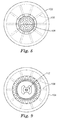
- light 42 can include, for example, LEDs 48, 50, 66, 68, 70, and 72 arranged around ring 46, as shown in FIG. 4 .
- the solid state light sources are in optical communication with optical guide 52; for example, the light sources can be located within hemispherical or other types of depressions in an edge of optical guide 52 and possibly secured through use of an optically clear adhesive.
- a base 44 is configured to connect to a power supply, and it can include a power circuit for providing the required voltage and current from the power supply to drive the solid state light sources.
- Base 44 can be implemented with, for example, an Edison base for use with conventional light bulb sockets or a base for use with conventional fluorescent light fixture connections.
- Air passages 56 and 58 are provided between optical guide 52 and base 44 to provide free convection across thermal guide 54 through an air passage 60.
- the thermal guide is implemented with metallic fins 54, 62, and 64, as illustrated in FIG. 3 .
- the fins are integrated with light guide 52, as shown in FIGS. 3 and 4 , in order to draw heat from solid state light sources 48, 50, 66, 68, 70, 72 and dissipate the heat through convection or radiation, or both, by air flow in air passage 60.
- the thermal guide can optionally include a heat pipe or thermal siphon.
- Optical guide 52 can be implemented with, for example, polycarbonate, polyacrylates such as polymethyl methacrylate, polystyrene, glass, or any number of different plastic materials having sufficiently high refractive indexes for the optical guide to distribute light.
- the exterior portion of light 42 can be used to distribute and emit light from the solid state light sources, and the interior portion of light 42 is used for cooling the thermal guide and solid state light sources.
- Optical guide 52 can be formed in a bulb shape, as represented in FIG. 2 , or in other shapes. With certain shapes, such as a bulb shape shown in FIG. 2 , the interior portion of optical guide 52 can form an interior volume, and the thermal guide can be integrated with the interior volume of the optical guide for providing thermal conduction from the solid state light sources.
- FIG. 5 is a cross sectional side view of a solid state light 74 with an active cooling element 88.
- Light 74 can have a similar construction as light 42.
- Light 74 includes a base 76, an optical guide 84, a thermal guide 86, and solid state light sources, such as LEDs 80 and 82, arranged on an optional heat spreader ring 78.
- Active cooling element 88 such as a fan, draws air through air passage 87 for cooling in addition to free convection and radiation.
- Active cooling element 88 can be coupled to a power source through base 76, and it can run continuously when light 74 is in operation or can include a temperature sensor to active it only when light 74 is above a certain temperature.
- FIG. 6 is an exploded perspective view of a solid state light 100 with a tapered optical guide.
- FIG. 7 is a perspective view of light 100 as assembled, and FIGS. 8 and 9 are top and bottom views, respectively, of light 100. The perspective view in FIG. 7 is looking at the side and top of light 100, which is generally symmetrical from a side view.
- Light 100 includes an optical guide comprised of upper and lower portions 102 and 104, an integrated thermal guide 106, a decorative light ring 108 containing a circuit 114 having solid state light sources, a base portion 110, and a base 112 for electrical connection to a power source such as via conventional light sockets as identified above or other sockets.
- the optical guide is shown as having two portions, it can alternatively have more than two portions or be composed of a single contiguous piece of material.
- thermal guide 106 connects with light ring 108 and base portion 110 in order to draw and dissipate heat from the solid state light sources.
- thermal guide 106 has a central core connected with external curved fins, which can conform to the shape of the optical guide.
- thermal guide 106 can optionally include a reflective coating on its exterior surface.
- a reflective layer can be optionally included on the inside surface of the optical guide, such as a reflective film or white paint, or a reflective layer can be positioned between the optical guide and the thermal guide.
- the components of light 100 can be implemented with the exemplary materials and components identified above.
- Light 100 can optionally include an active cooling element as illustrated in FIG. 5 .
- the top edge of upper portion 102, forming air passage 101, can be lined with a reflective film 105 (shown in FIG. 8 ) so that light traversing the optical guide is reflected back down the guide when it reaches the top edge in order to be distributed through the exterior or interior surfaces of the optical guide.
- a reflective film is the Enhanced Specular Reflector (ESR) film product from 3M Company, St. Paul, Minnesota.
- Circuitry 116 such as a printed circuit board, can be mounted in the central core of thermal guide 106 such as within a slot as shown in FIG. 7 . When mounted, circuitry 116 is electrically connected with solid state light sources on circuit 114 and base 112. Circuitry 116 receives power from a power supply via base 112 and provides the required voltage and current to drive the solid state light sources. Circuitry 116 can be thermally coupled to the thermal guide in order to help cool the electronic components.
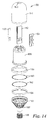
- FIG. 10 is an exploded perspective view of an LED assembly for light 100.
- Solid state light sources 120 such as LEDs, are mounted on circuit 114 and contained within light ring 108.
- the LED circuit in the light ring can comprise any combination of alternating dielectric layers and conductive circuit paths that connect the LEDs and electrically isolate the LED circuit from light ring 108.
- Light ring 108 can be composed of a metal material such as aluminum.
- a pair of concentric reflective rings 118 are mounted in the circular slot of light ring 108 and over the solid state light sources 120. Reflective rings 118 help inject light from light sources 120 into lower portion 104 of the optical guide.
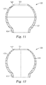
- FIG. 11 is a cross sectional side view of a first tapered optical guide 122 for implementing upper portion 102 and lower portion 104 of the optical guide for light 100.
- Optical guide 122 includes a upper portion 121 that mates with a lower portion 123 with a horizontal seam parallel to light ring 108.
- Upper portion 121 includes an air passage 125 providing for air flow across the thermal guide.
- the thickness of lower portion 123 is substantially constant from bottom edge 124, while the thickness of upper portion 121 tapers from the thickness of lower portion 123 to a top edge 126.
- Upper portion 121 thus becomes thinner moving away from the solid state light sources, which enhances light extraction and distribution.
- This type of taper involves a discontinuous taper, meaning only a portion of the optical guide is tapered.
- FIG. 12 is a cross sectional side view of a second tapered optical guide 128 as an alternative embodiment of the optical guide for light 100.
- Optical guide 128 includes a left portion 127 that mates with a right portion 129 with a vertical seam perpendicular to light ring 108.
- Left and right portions 127 and 129 together form an air passage 131 providing for air flow across the thermal guide.
- Left portion 127 tapers from a bottom edge 130 to a top edge 132, and right portion 129 tapers in a likewise manner. Therefore, this optical guide becomes thinner from the bottom edge to the top edge of each portion moving away from the solid state light sources, which enhances light extraction and distribution.
- This type of taper involves a continuous taper, meaning the entire optical guide is tapered.
- the amount of taper can be varied based upon a desired distribution of light output, for example, and the amount of tapering can be determined using empirical evidence, modeling, or other techniques. Also, a discontinuous or continuous taper can be applied to the optical guide whether it includes upper and lower portions, right and left portions, or other types of portions.
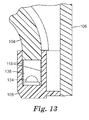
- FIG. 13 is a cross sectional side view illustrating light injection for light 100.
- Solid state light sources 120 such as an LED 134
- the bottom edge of lower portion 104 of the optical guide is mounted in light ring 108 and on reflective rings 118, forming an air gap 138 between LED 134 and the bottom edge of lower portion 104 of the optical guide.
- Light from LED 134 is injected into the bottom edge of lower portion 104 and distributed by the optical guide.
- FIG. 14 is an exploded perspective view of a solid state light 150 with a thermal guide having an exterior shell.
- FIG. 15 is a cross sectional side view of light 150.
- FIGS. 16 and 17 are top and bottom views, respectively, of light 150.
- Light 150 is generally symmetrical from a side view.
- Light 150 includes a cylindrical optical guide 151, an integrated thermal guide 156, a solid state light assembly, a decorative base ring 166, and a base 168 for electrical connection to a power source such as via conventional light sockets as identified above or other sockets. At least a portion of, or possible the entire, optical guide 151 can optionally be tapered.
- the components of light 150 can be implemented with the exemplary materials and components identified above.
- thermal guide 156 is shown having a cylindrical shape, other shapes are possible while still having an exterior shell. Also, thermal guide 156 can optionally include a reflective coating on its exterior surface. One type of reflective coating reflects visible light and emits infrared (IR) light. Light 150 can optionally include an active cooling element as illustrated in FIG. 5 .
- the top edge of optical guide 151, forming air passage 153, can be lined with a reflective film 155 (shown in FIG. 16 ), such as ESR film so that light traversing the optical guide is reflected back down the guide when it reaches the top edge in order to be distributed through the exterior or interior surfaces of the optical guide.
- the solid state light assembly includes a pair of concentric reflective rings 158, solid state light sources 160, a circuit 162, and a light ring 164.
- Solid state light sources 160 such as LEDs, are contained on circuit 162 for driving the solid state light sources.
- Light ring 164 includes a partial wedge shaped recess for containing circuit 162, and light ring 164 is positioned in a recess in base ring 166.
- Reflective rings 158 are mounted in the slot in light ring 164 and over solid state light sources 160. Reflective rings 158 help inject light from light sources 160 into a bottom edge of optical guide 151.
- Circuitry 153 and 154 can be secured to a circuit holder 152 and mounted in the center of thermal guide 156 such as within a slot. When mounted, circuitry 153 and 154 are electrically connected with solid state light sources on circuit 162 and base 168. Circuitry 153 and 154 receive power from a power supply via base 168 and provides the required voltage and current to drive the solid state light sources. Circuitry 153 and 154 can be thermally coupled to the thermal guide in order to help cool the electronic components.
- FIG. 18 is a perspective view of thermal guide 156.
- FIGS. 19 and 20 are side and top views, respectively, of thermal guide 156.
- Thermal guide 156 includes an exterior shell 170 containing internal fins 172, curved at the top to conform to the curved top portion of optical guide 151.
- a core section 174 is connected to the fins and contains a slot for accommodating circuit holder 152.
- Use of exterior shell 170 provides for a back reflector to optical guide 151 such that light from optical guide 151 into the interior of light 150 is reflected back through optical guide 151, enhancing the light output.
- the exterior of shell 170 can be covered with a reflective coating or paint such as the Starbrite II water primer from Spraylat Corporation, Chicago, Illinois, which provides a white surface finish.
- a reflective coating or paint reflects visible light and emits IR light.
- FIG. 21 is a perspective view of a thermal guide 176 as an alternative embodiment of the thermal guide for light 151.
- FIGS. 22 and 23 are side and top views, respectively, of thermal guide 176.
- Thermal guide 176 includes an interior shell 177 containing external fins 178, curved at the top to conform to the top portion of optical guide 151.
- a core section 180 is part of interior shell 177 and contains a slot for accommodating circuit holder 152.
- Thermal guide 176 has exterior fins adjacent the inside of optical guide 151.
- FIG. 24 is a cross sectional side view illustrating light injection for light 150.
- Solid state light sources 160 such as an LED 182 are mounted within light ring 164 and between reflective rings 158.
- the bottom edge of optical guide 151 forms a wedge portion 186 mounted in light ring 164 and between reflective rings 158.
- the portions of light ring 164 adjacent wedge portion 186 can have a high reflectivity surface, and reflective rings 158 can be optically coupled, or not optically coupled, to wedge portion 186 of the optical guide.
- the bottom edge of wedge portion 186 is shaped to conform to the shape of LED 182, in this embodiment a round curved shape, although other shapes can be used depending upon the shape of the solid state light source.
- Light from LED 182 is injected into the bottom edge of wedge portion 186 of optical guide 151 and distributed by the optical guide.
- the optical guide can optionally be potted or adhered to LED 182 using silicone, acrylic, or other materials.
- thermal guide 156 and light ring 164 nest into base ring 166, and a curved portion 183 of base ring 166 "snaps" around a top edge 185 of light ring 164.
- FIGS. 25 and 26 are top views illustrating examples of optional patterns of extraction features for the optical guide, portions 102 and 104, in light 100. These extraction patterns, or other such patterns, can be applied to the interior or exterior surfaces, or both, of the optical guide for efficient and substantially uniform angular distribution of light emitted by the optical guide. Alternatively, other extraction patterns may be applied to produce non-uniform but desirable distribution of light from the optical guide.
- FIG. 25 illustrates a substantially uniform extraction pattern with a slight variation in extraction feature density.
- FIG. 26 illustrates a more non-uniform pattern to compensate for the tight radius that the light has to traverse upon being emitted by the LEDs and traveling up lower portion 104 of the optical guide.
- the extraction patterns can be applied to the exterior or interior surfaces, or both, of the optical guide as painted white dots using a mask with a corresponding pattern.
- the exterior or interior surfaces of the optical guide can include a uniform white coating.
- Light 150 can also optionally include an extraction pattern applied to the exterior or interior surfaces, or both, of optical guide 151.
- a light bulb was produced in accordance with FIGS. 6-11 and 13 .
- the light ring subassembly ( FIG. 10 ) is the light engine of the LED bulb design. It includes an LED circuit assembly typically comprising 9 Nichia NCSW119T (or equivalent) white LEDs soldered to a flexible circuit comprising 18 micron copper on 1 mil (0.001 inches) thick polyimide or other polymer substrate.
- This flexible circuit was laminated to an aluminum ring component (light ring 108 in FIGS. 6 , 7 , and 10 ) using 3M TC 2810 thermally conductive epoxy adhesive (3M Company) applied to produce a very thin bond line (approximately 0.001 inches or thinner) that enhances thermal conductivity between the LEDs and the aluminum ring.
- the aluminum ring was machined out of an aluminum block in accordance with FIG. 10 .
- the exterior of the aluminum light ring was painted white by spraying a thin coating of the Starbrite II ZR-6221 product from Spraylat Corporation, Chicago, Illinois, diluted with 30% water.
- the aluminum ring is the primary thermal path from the LEDs, through the flex circuit, to the thermal guide in the light design.
- the Vikuiti ESR film from 3M Company was laminated to the side walls of the light ring subassembly.
- the ESR film is disposed as shown in FIGS. 10 and 13 .
- thermal guide 106 An aluminum thermal guide was then machined in accordance with FIG. 6 (thermal guide 106).
- the thermal guide was painted white by spraying it with a thin coating of the Starbrite II ZR-6221 product diluted with 30% water.
- the section of the thermal guide below the fins was not painted white.
- the light guides were fabricated by machining a block of clear cast acrylic in accordance with FIGS. 6 and 7 (optical guide formed by upper and lower portions 102 and 104).
- the light guides were still rough after machining.
- the interior and exterior surfaces were polished using the 3M Headlight Restoration Kit product (3M Company).
- the recommended step by step procedure was followed, resulting in a clear top and bottom light guides.
- the edges of the light guide were flattened and polished by lapping the surfaces smooth and flat.
- a mask was applied to the interior of the light guides, which had a desired hole pattern.
- the interior surface including the adhered mask was then painted white by spraying a thin coating of the Starbrite II ZR-6221 product diluted with 30% water over the entire interior surface of the light guides.
- the paint was allowed to partially dry, which took about 10 minutes.
- the mask was then removed from the interior surface.
- the areas where the holes were retained the white Starbrite coating, leaving dots of white paint that acted as a light extraction pattern on the inside
- the bottom light guide was inserted 2-3 mm into the light ring (light ring 108 in FIGS. 6 , 7 , and 10 ).
- the light guide was pressed into place using the Carver Laboratory Press Model C product from Carver, Inc., Wabash, Indiana. The distance the light guide was inserted into the light ring was measured using a scale as the light guide was inserted into the light ring.
- the light ring and light guide subassembly was then pressed onto the thermal guide using the Carver Laboratory Press Model C product. The subassembly was pressed onto the thermal guide until 9-10 mm of the bottom of the thermal guide was protruding out from the light ring subassembly.
- top half of the light guide was applied to the subassembly described above.
- a pressure sensitive adhesive was used to form the bond between the top and bottom light guide halves (upper and lower portions 102 and 104 in FIGS. 6 and 7 ).
- the adhesive that was used to laminate the top half of the light guide to bottom half was 3M Optically Clear Adhesive 8187 (3M Company). This adhesive is supplied as a 0.007 inch thick adhesive with a release liner on both sides. An approximately 4 inch x 4 inch square of 8187 adhesive was used to bond the two pieces of the light guide. The release liner was removed from one side of the adhesive and laid on a hard flat surface with the exposed adhesive facing up.
- the laminating edge of the light guide was cleaned with a soft cloth and isopropyl alcohol.
- the light guide was then pressed firmly onto the exposed adhesive. While pressing down on the light guide, the excess adhesive was trimmed from the outside edge with a scalpel.
- the light guide was then turned over and the excess adhesive on the interior of the light guide was trimmed away with a scalpel leaving a thin ring of adhesive laminated to the light guide covered with a release liner.
- the bottom half of the light guide was positioned with three firm contact points at approximately 120° apart along the perimeter of the light guide.
- the release liner was removed from the top light guide and slowly lowered over the bottom light guide using the three contact points to guide the alignment. After the guides were laminated, pressure was applied for one minute to ensure complete optical coupling of the guides by the adhesive.
- the primary bulb thermal guide was drilled and tapped near the base, and the Delrin insulator base was drilled for clearance so that one of the Delrin tabs that was inserted into the heat sink could be locked to the heat sink, preventing it from sliding out or twisting when the bulb was screwed into an Edison socket.
- the remaining 3 tabs of the Delrin mount were trimmed as needed with a heat knife to allow more room for the electronics.
- solder lugs and Edison screw base (base 112 in FIGS. 6 and 7 ) were attached to the Delrin insulating base prior to installation. Two wires were soldered to the base that would later be connected to the circuit board.
- a secondary heat coupler was fabricated to thermally couple the hottest components (the bridge rectifier, a transistor - used in the TRIAC holding current portion of the circuit, the switching transistor, and the flyback diode) to the thermal guide, using the Thermally Conductive Adhesive Transfer Tape 8820 product (3M Company).
- the heat coupler was machined to match the radius of the inner diameter of the thermal guide while connecting intimately with the four circuit components.
- thermally conductive grease (Wakefield 120 Thermal Compound product) was applied to the coupler's exterior surface such that excellent heat transfer was established between the electronics and the primary thermal guide. Before the electronics were finally inserted, the wires from the LEDs were soldered to the circuit board's output terminals.
- the board was then inserted from the top and pushed through such that the board protruded from the bottom of the bulb base.
- the wires from the Edison base were then soldered to the board and tucked inside the base as the base was inserted into the heat sink. A screw then locked the base to the thermal guide.
Description
- The energy efficiency of lighting has become an important consideration in industrial, consumer, and architectural lighting applications. With the advances in solid state light technology, light emitting diodes (LEDs) have become more energy efficient than fluorescent lights. Further, the marketplace has a large established fixture base for Edison, fluorescent and high intensity discharge lights. These types of applications present a significant technical challenge for LEDs due to their inherent point source nature, and the need to operate the LEDs at relatively low temperatures. Today there are many solutions addressing these issues, including fans, thermal sinks, heat pipes and the like.
-
KR 100 961 840 B1 - However, these approaches limit the applications by adding complexity, cost, efficiency loss, added failure modes, and an undesirable form factor. The need remains to find a solution that can provide optical and electrical efficiency benefits, at attractive manufacturing costs and design.
- The present invention is defined by the subject-matter of
claim 1. - A light, consistent with the present invention, includes a light source, an optical guide, and a thermal guide. The optical guide is coupled to the light source for receiving and distributing light from the light source, and the thermal guide is integrated with the optical guide for providing thermal conduction from the light source for cooling the light.
- In one embodiment, the optical guide is tapered to enhance the efficiency of light distribution. In another embodiment, the thermal guide has an external shell connected with internal fins, and the external shell can have a reflective coating to provide for a back reflector behind the optical guide.
- The accompanying drawings are incorporated in and constitute a part of this specification and, together with the description, explain the advantages and principles of the invention. In the drawings,
-
FIG. 1 is a diagram illustrating a solid state light source with an optical guide and integrated thermal guide; -
FIG. 2 is a cross sectional side view of a solid state light using an optical guide having an exterior portion for emitting light and an interior portion for cooling; -
FIG. 3 is a top view of the light ofFIG. 2 ; -
FIG. 4 is a bottom view of the light ofFIG. 2 ; -
FIG. 5 is a cross sectional side view of a solid state light with an active cooling element; -
FIG. 6 is an exploded perspective view of a solid state light with a tapered optical guide; -
FIG. 7 is a perspective view of the light ofFIG. 6 as assembled; -
FIG. 8 is a top view of the light ofFIG. 6 ; -
FIG. 9 is a bottom view of the light ofFIG. 6 ; -
FIG. 10 is an exploded perspective view of an LED assembly for the light ofFIG. 6 ; -
FIG. 11 is a cross sectional side view of a first tapered optical guide; -
FIG. 12 is a cross sectional side view of a second tapered optical guide; -
FIG. 13 is a cross sectional side view illustrating light injection for the light ofFIG. 6 ; -
FIG. 14 is an exploded perspective view of a solid state light with a thermal guide having an exterior shell; -
FIG. 15 is a cross sectional side view of the light ofFIG. 14 ; -
FIG. 16 is a top view of the light ofFIG. 14 ; -
FIG. 17 is a bottom view of the light ofFIG. 14 ; -
FIG. 18 is a perspective view of a first thermal guide for the light ofFIG. 14 ; -
FIG. 19 is a side view of the first thermal guide; -
FIG. 20 is a top view of the first thermal guide; -
FIG. 21 is a perspective view of a second thermal guide for the light ofFIG. 14 ; -
FIG. 22 is a side view of the second thermal guide; -
FIG. 23 is a top view of the second thermal guide; -
FIG. 24 is a cross sectional side view illustrating light injection for the light ofFIG. 14 ; -
FIG. 25 is a first extraction pattern for the optical guide; and -
FIG. 26 is a second extraction pattern for the optical guide. -
FIG. 1 is a diagram illustrating components of alight 10 having apower circuit 12, a solidstate light source 14, and a thermo-optical guide comprising anoptical guide 16 and an integratedthermal guide 18.Power circuit 12 receives power from a power supply and provides the required voltage and current to drive solidstate light source 14, which is in optical communication withoptical guide 16.Power circuit 12 is an optional element oflight 10, if the power supply is configured to provide the required voltage and current directly tolight 10 or if the circuit is external to light 10. Solidstate light source 14 injects light intooptical guide 16, which receives and distributes the light.Optical guide 16 includes light injection, light transport, and light extraction zones or elements in order to distribute the light.Thermal guide 18 is integrated withoptical guide 16 in order to draw heat from solidstate light source 14 through conduction and dissipate the heat through convection or radiation, or both, to coollight 10 and to efficiently utilize both area and volume for the cooling.Thermal guide 18 includes heat acquisition, heat spreading, and heat dissipation zones or elements in order to cool the light. Through integration of the optical and thermal guides, embodiments of this invention overcome many of the limitations of current solid state light concepts such as those identified above. - Solid
state light source 14 can be implemented with, for example, LEDs, organic light emitting diodes (OLEDs), or other solid state light sources. Certain embodiments can provide for uniformly distributed light from the solid state light source. Alternatively, embodiments may be employed to control or direct light in a particular distribution. In one example, refraction can be used to control the emitted light; for example, lenses may be used to focus the light or reflectors may be used to concentrate or spread the light. For example, in certain embodiments the light can produce a cone or curtain of light. The lenses could have air permeability for cooling and can include Fresnel lenses, prismatic structures, or lenslet structures. In other embodiments, diffractive optics may be employed to control or direct both the spectrum and the distribution of the emitted light. For example, a diffractive lens may be used to direct a particular light distribution, or color from a broad light distribution, in a particular direction. Also, combinations of diffractive and refractive optics may be used. - The solid state light sources can emit light of various colors for decorative or other lighting effects. Solid
state light source 14 is electrically connected withpower circuit 12, which can include a flexible circuit or other circuitry for powering the solid state light source. The circuitry to power the light source can include dimming circuitry and electronics to control frequency shifting or color shifting components that help produce a more desirable light, and an example of such electronics are described inU.S. Patent Application Publication No. 2009/0309505 . -
Optical guide 16 can be implemented with, for example, a transparent or translucent material capable of receiving light from the solid state light source and emitting the light. For example,optical guide 16 preferably is made of an optically suitable material such as polycarbonate, polyacrylates such as polymethyl methacrylate, polystyrene, glass, or any number of different plastic materials having sufficiently high refractive indexes for the optical guide to distribute light. The optical guide can be configured in a variety of shapes such as a bulb, sphere, cylinder, cube, sheet, or other shape. Furthermore, the optical guide can include a matrix material that can contain light frequency shifting material to obtain a more desirable color, and examples of matrix stabilized dyes are described inU.S. Patent No. 5,387,458 . -
Thermal guide 18 can be implemented with a material capable of conducting heat from the solid state light source and dissipating the heat. For example, the thermal guide is preferably comprised of a material with a thermal conductivity from about 1W/(m-K) to 1000 W/(m-K), and more preferably from 10 W/(m-K) to 1000 W/(m-K), and most preferable from 100 W/(m-K) to 1000 W/(m-K). The thermal guide draws heat from the solid state light source through conduction and dissipates heat into air through convection or radiation, or both. Optionally, components of the thermal guide can include heat pipes and thermal siphons. Optionally, the thermal guide, or a portion thereof, can include a thermally conductive coating on the surfaces of the solid state light source; for example, carbon nanaotubes that can transport heat from the solid state light source through conduction and convection may be coated onto the surfaces. - The thermal guide is integrated with the optical guide, meaning that the thermal guide is in sufficient contact, directly or indirectly, with the solid state light source in order to conduct and dissipate heat from the solid state light source for the light to function. For example, the thermal guide can draw heat from the solid state light sources to maintain the light sources cool enough to function as intended. The thermal guide can be directly in physical contact with the solid state light sources or indirectly in contact with them such as through a ring or other components upon which the solid state light sources are mounted. An air gap is formed between at least a portion of the thermal guide and a surface of the optical guide, which air gap substantially surrounds the thermal guide between the thermal guide and said surface of the optical guide. Therefore, the thermal guide resides either co-extensively proximate to at least a portion or preferably a majority of the area of the optical guide, or the thermal guide resides within at least a portion or preferably a majority of the volume of the optical guide in the case of a bulb, sphere or other three dimensional shape having an interior volume.
- The thermal guide can include thermal conductivity enhancements such as metal coatings or layers, or conductive particles, to help conduct the heat generated by the solid state light sources into and along the thermal guide. Further, the thermal guide can have convective thermal enhancements such as fins and microstructures to increase the convection and radiation heat transfer coefficient. The thermal guide can also have optical enhancements in order to enhance the light output of the optical guide. For example, the thermal guide can be formed from a reflective material or a material modified to have a reflective surface such as white paint, a polished surface, or a thin reflective material on its surface. The reflective surface can also be made from a material with high infrared emissivity in order to increase heat dissipation to the surroundings by thermal radiation.
- An example of a solid state light is disclosed in
U.S. Patent Application Serial No. 12/535203 U.S. Patent Application Serial No. 12/829611 -
FIG. 2 is a cross sectional side view of an embodiment of a solid state light 42 using an optical guide having an exterior portion for emitting light and an interior portion for cooling.FIGS. 3 and4 are top and bottom views, respectively oflight 42.Light 42 includes anoptical guide 52, integratedthermal guide 54, and solid state light sources on an optionalheat spreader ring 46. Theheat spreader ring 46 can operate by thermal conduction or have a heat pipe or thermal siphon associated with it. The heat spreader ring contains elements that efficiently connect to the thermal guide, an example of which includes a ring containing bent fin elements that are thermally connected to the thermal guide. Alternatively, the solid state light sources can be coupled directly to a thermal guide without a heat spreader ring. For the solid state light sources, light 42 can include, for example,LEDs ring 46, as shown inFIG. 4 . The solid state light sources are in optical communication withoptical guide 52; for example, the light sources can be located within hemispherical or other types of depressions in an edge ofoptical guide 52 and possibly secured through use of an optically clear adhesive. - A
base 44 is configured to connect to a power supply, and it can include a power circuit for providing the required voltage and current from the power supply to drive the solid state light sources.Base 44 can be implemented with, for example, an Edison base for use with conventional light bulb sockets or a base for use with conventional fluorescent light fixture connections.Air passages optical guide 52 andbase 44 to provide free convection acrossthermal guide 54 through anair passage 60. - In this exemplary embodiment, the thermal guide is implemented with
metallic fins FIG. 3 . The fins are integrated withlight guide 52, as shown inFIGS. 3 and4 , in order to draw heat from solid statelight sources air passage 60. The thermal guide can optionally include a heat pipe or thermal siphon.Optical guide 52 can be implemented with, for example, polycarbonate, polyacrylates such as polymethyl methacrylate, polystyrene, glass, or any number of different plastic materials having sufficiently high refractive indexes for the optical guide to distribute light. The exterior portion of light 42 can be used to distribute and emit light from the solid state light sources, and the interior portion oflight 42 is used for cooling the thermal guide and solid state light sources.Optical guide 52 can be formed in a bulb shape, as represented inFIG. 2 , or in other shapes. With certain shapes, such as a bulb shape shown inFIG. 2 , the interior portion ofoptical guide 52 can form an interior volume, and the thermal guide can be integrated with the interior volume of the optical guide for providing thermal conduction from the solid state light sources. -
FIG. 5 is a cross sectional side view of a solid state light 74 with anactive cooling element 88.Light 74 can have a similar construction aslight 42.Light 74 includes abase 76, anoptical guide 84, athermal guide 86, and solid state light sources, such asLEDs heat spreader ring 78.Active cooling element 88, such as a fan, draws air throughair passage 87 for cooling in addition to free convection and radiation.Active cooling element 88 can be coupled to a power source throughbase 76, and it can run continuously when light 74 is in operation or can include a temperature sensor to active it only when light 74 is above a certain temperature. -
FIG. 6 is an exploded perspective view of a solid state light 100 with a tapered optical guide.FIG. 7 is a perspective view oflight 100 as assembled, andFIGS. 8 and 9 are top and bottom views, respectively, oflight 100. The perspective view inFIG. 7 is looking at the side and top oflight 100, which is generally symmetrical from a side view.Light 100 includes an optical guide comprised of upper andlower portions thermal guide 106, a decorativelight ring 108 containing acircuit 114 having solid state light sources, abase portion 110, and abase 112 for electrical connection to a power source such as via conventional light sockets as identified above or other sockets. Although the optical guide is shown as having two portions, it can alternatively have more than two portions or be composed of a single contiguous piece of material. - As illustrated in
FIG. 7 ,upper portion 102 mates withlower portion 104 to form the optical guide, andlower portion 104 mounts tolight ring 108 in order to optically couple with solid state light sources oncircuit 114. The optical guide in this embodiment has a doubly curved shape.Thermal guide 106 connects withlight ring 108 andbase portion 110 in order to draw and dissipate heat from the solid state light sources. As shown inFIG. 6 ,thermal guide 106 has a central core connected with external curved fins, which can conform to the shape of the optical guide. Also,thermal guide 106 can optionally include a reflective coating on its exterior surface. Furthermore, in any of the embodiments a reflective layer can be optionally included on the inside surface of the optical guide, such as a reflective film or white paint, or a reflective layer can be positioned between the optical guide and the thermal guide. The components of light 100 can be implemented with the exemplary materials and components identified above.Light 100 can optionally include an active cooling element as illustrated inFIG. 5 . - An
air passage 101 inupper portion 102 along withapertures 107 inlight ring 108 allow air flow acrossthermal guide 106, and this type of air flow is illustrated by the arrows inFIG. 2 . The top edge ofupper portion 102, formingair passage 101, can be lined with a reflective film 105 (shown inFIG. 8 ) so that light traversing the optical guide is reflected back down the guide when it reaches the top edge in order to be distributed through the exterior or interior surfaces of the optical guide. An example of a reflective film is the Enhanced Specular Reflector (ESR) film product from 3M Company, St. Paul, Minnesota. -
Circuitry 116, such as a printed circuit board, can be mounted in the central core ofthermal guide 106 such as within a slot as shown inFIG. 7 . When mounted,circuitry 116 is electrically connected with solid state light sources oncircuit 114 andbase 112.Circuitry 116 receives power from a power supply viabase 112 and provides the required voltage and current to drive the solid state light sources.Circuitry 116 can be thermally coupled to the thermal guide in order to help cool the electronic components. -
FIG. 10 is an exploded perspective view of an LED assembly forlight 100. Solid statelight sources 120, such as LEDs, are mounted oncircuit 114 and contained withinlight ring 108. Alternately, the LED circuit in the light ring can comprise any combination of alternating dielectric layers and conductive circuit paths that connect the LEDs and electrically isolate the LED circuit fromlight ring 108.Light ring 108 can be composed of a metal material such as aluminum. A pair of concentricreflective rings 118 are mounted in the circular slot oflight ring 108 and over the solid statelight sources 120.Reflective rings 118 help inject light fromlight sources 120 intolower portion 104 of the optical guide. -
FIG. 11 is a cross sectional side view of a first taperedoptical guide 122 for implementingupper portion 102 andlower portion 104 of the optical guide forlight 100.Optical guide 122 includes aupper portion 121 that mates with alower portion 123 with a horizontal seam parallel tolight ring 108.Upper portion 121 includes anair passage 125 providing for air flow across the thermal guide. The thickness oflower portion 123 is substantially constant frombottom edge 124, while the thickness ofupper portion 121 tapers from the thickness oflower portion 123 to atop edge 126.Upper portion 121 thus becomes thinner moving away from the solid state light sources, which enhances light extraction and distribution. This type of taper involves a discontinuous taper, meaning only a portion of the optical guide is tapered. -
FIG. 12 is a cross sectional side view of a second taperedoptical guide 128 as an alternative embodiment of the optical guide forlight 100.Optical guide 128 includes aleft portion 127 that mates with aright portion 129 with a vertical seam perpendicular tolight ring 108. Left andright portions air passage 131 providing for air flow across the thermal guide.Left portion 127 tapers from abottom edge 130 to atop edge 132, andright portion 129 tapers in a likewise manner. Therefore, this optical guide becomes thinner from the bottom edge to the top edge of each portion moving away from the solid state light sources, which enhances light extraction and distribution. This type of taper involves a continuous taper, meaning the entire optical guide is tapered. For either a discontinuous or continuous taper, the amount of taper can be varied based upon a desired distribution of light output, for example, and the amount of tapering can be determined using empirical evidence, modeling, or other techniques. Also, a discontinuous or continuous taper can be applied to the optical guide whether it includes upper and lower portions, right and left portions, or other types of portions. -
FIG. 13 is a cross sectional side view illustrating light injection forlight 100. Solid statelight sources 120, such as anLED 134, are mounted withinlight ring 108 and betweenreflective rings 118. The bottom edge oflower portion 104 of the optical guide is mounted inlight ring 108 and onreflective rings 118, forming anair gap 138 betweenLED 134 and the bottom edge oflower portion 104 of the optical guide. Light fromLED 134 is injected into the bottom edge oflower portion 104 and distributed by the optical guide. -
FIG. 14 is an exploded perspective view of a solid state light 150 with a thermal guide having an exterior shell.FIG. 15 is a cross sectional side view oflight 150.FIGS. 16 and 17 are top and bottom views, respectively, oflight 150.Light 150 is generally symmetrical from a side view.Light 150 includes a cylindricaloptical guide 151, an integratedthermal guide 156, a solid state light assembly, adecorative base ring 166, and abase 168 for electrical connection to a power source such as via conventional light sockets as identified above or other sockets. At least a portion of, or possible the entire,optical guide 151 can optionally be tapered. The components of light 150 can be implemented with the exemplary materials and components identified above. Althoughthermal guide 156 is shown having a cylindrical shape, other shapes are possible while still having an exterior shell. Also,thermal guide 156 can optionally include a reflective coating on its exterior surface. One type of reflective coating reflects visible light and emits infrared (IR) light.Light 150 can optionally include an active cooling element as illustrated inFIG. 5 . - An
air passage 153 inoptical guide 151 along withapertures 167 inbase ring 166 allow air flow acrossthermal guide 156, and this type of air flow is illustrated by the arrows inFIG. 2 . The top edge ofoptical guide 151, formingair passage 153, can be lined with a reflective film 155 (shown inFIG. 16 ), such as ESR film so that light traversing the optical guide is reflected back down the guide when it reaches the top edge in order to be distributed through the exterior or interior surfaces of the optical guide. - The solid state light assembly includes a pair of concentric
reflective rings 158, solid statelight sources 160, acircuit 162, and alight ring 164. Solid statelight sources 160, such as LEDs, are contained oncircuit 162 for driving the solid state light sources.Light ring 164 includes a partial wedge shaped recess for containingcircuit 162, andlight ring 164 is positioned in a recess inbase ring 166.Reflective rings 158 are mounted in the slot inlight ring 164 and over solid statelight sources 160.Reflective rings 158 help inject light fromlight sources 160 into a bottom edge ofoptical guide 151. -
Circuitry circuit holder 152 and mounted in the center ofthermal guide 156 such as within a slot. When mounted,circuitry circuit 162 andbase 168.Circuitry base 168 and provides the required voltage and current to drive the solid state light sources.Circuitry -
FIG. 18 is a perspective view ofthermal guide 156.FIGS. 19 and20 are side and top views, respectively, ofthermal guide 156.Thermal guide 156 includes anexterior shell 170 containinginternal fins 172, curved at the top to conform to the curved top portion ofoptical guide 151. Acore section 174 is connected to the fins and contains a slot for accommodatingcircuit holder 152. Use ofexterior shell 170 provides for a back reflector tooptical guide 151 such that light fromoptical guide 151 into the interior of light 150 is reflected back throughoptical guide 151, enhancing the light output. The exterior ofshell 170 can be covered with a reflective coating or paint such as the Starbrite II water primer from Spraylat Corporation, Chicago, Illinois, which provides a white surface finish. One type of reflective coating or paint reflects visible light and emits IR light. -
FIG. 21 is a perspective view of athermal guide 176 as an alternative embodiment of the thermal guide forlight 151.FIGS. 22 and 23 are side and top views, respectively, ofthermal guide 176.Thermal guide 176 includes aninterior shell 177 containingexternal fins 178, curved at the top to conform to the top portion ofoptical guide 151. Acore section 180 is part ofinterior shell 177 and contains a slot for accommodatingcircuit holder 152.Thermal guide 176 has exterior fins adjacent the inside ofoptical guide 151. -
FIG. 24 is a cross sectional side view illustrating light injection forlight 150. Solid statelight sources 160, such as anLED 182, are mounted withinlight ring 164 and betweenreflective rings 158. The bottom edge ofoptical guide 151 forms awedge portion 186 mounted inlight ring 164 and betweenreflective rings 158. The portions oflight ring 164adjacent wedge portion 186 can have a high reflectivity surface, andreflective rings 158 can be optically coupled, or not optically coupled, to wedgeportion 186 of the optical guide. The bottom edge ofwedge portion 186 is shaped to conform to the shape ofLED 182, in this embodiment a round curved shape, although other shapes can be used depending upon the shape of the solid state light source. Light fromLED 182 is injected into the bottom edge ofwedge portion 186 ofoptical guide 151 and distributed by the optical guide. The optical guide can optionally be potted or adhered toLED 182 using silicone, acrylic, or other materials. To secure the components,thermal guide 156 andlight ring 164 nest intobase ring 166, and acurved portion 183 ofbase ring 166 "snaps" around atop edge 185 oflight ring 164. -
FIGS. 25 and 26 are top views illustrating examples of optional patterns of extraction features for the optical guide,portions light 100. These extraction patterns, or other such patterns, can be applied to the interior or exterior surfaces, or both, of the optical guide for efficient and substantially uniform angular distribution of light emitted by the optical guide. Alternatively, other extraction patterns may be applied to produce non-uniform but desirable distribution of light from the optical guide.FIG. 25 illustrates a substantially uniform extraction pattern with a slight variation in extraction feature density.FIG. 26 illustrates a more non-uniform pattern to compensate for the tight radius that the light has to traverse upon being emitted by the LEDs and traveling uplower portion 104 of the optical guide. - The extraction patterns can be applied to the exterior or interior surfaces, or both, of the optical guide as painted white dots using a mask with a corresponding pattern. As an alternative to a dot pattern, the exterior or interior surfaces of the optical guide can include a uniform white coating.
Light 150 can also optionally include an extraction pattern applied to the exterior or interior surfaces, or both, ofoptical guide 151. - A light bulb was produced in accordance with
FIGS. 6-11 and13 . - The light ring subassembly (
FIG. 10 ) is the light engine of the LED bulb design. It includes an LED circuit assembly typically comprising 9 Nichia NCSW119T (or equivalent) white LEDs soldered to a flexible circuit comprising 18 micron copper on 1 mil (0.001 inches) thick polyimide or other polymer substrate. This flexible circuit was laminated to an aluminum ring component (light ring 108 inFIGS. 6 ,7 , and10 ) using 3M TC 2810 thermally conductive epoxy adhesive (3M Company) applied to produce a very thin bond line (approximately 0.001 inches or thinner) that enhances thermal conductivity between the LEDs and the aluminum ring. The aluminum ring was machined out of an aluminum block in accordance withFIG. 10 . Prior to mounting the LEDs in the light ring, the exterior of the aluminum light ring was painted white by spraying a thin coating of the Starbrite II ZR-6221 product from Spraylat Corporation, Chicago, Illinois, diluted with 30% water. The aluminum ring is the primary thermal path from the LEDs, through the flex circuit, to the thermal guide in the light design. - Once the LEDs were bonded into the light ring, the Vikuiti ESR film from 3M Company was laminated to the side walls of the light ring subassembly. The ESR film is disposed as shown in
FIGS. 10 and13 . - An aluminum thermal guide was then machined in accordance with
FIG. 6 (thermal guide 106). The thermal guide was painted white by spraying it with a thin coating of the Starbrite II ZR-6221 product diluted with 30% water. The section of the thermal guide below the fins was not painted white. - Next the light guides were fabricated by machining a block of clear cast acrylic in accordance with
FIGS. 6 and7 (optical guide formed by upper andlower portions 102 and 104). The light guides were still rough after machining. The interior and exterior surfaces were polished using the 3M Headlight Restoration Kit product (3M Company). The recommended step by step procedure was followed, resulting in a clear top and bottom light guides. Next the edges of the light guide were flattened and polished by lapping the surfaces smooth and flat. Next a mask was applied to the interior of the light guides, which had a desired hole pattern. The interior surface including the adhered mask was then painted white by spraying a thin coating of the Starbrite II ZR-6221 product diluted with 30% water over the entire interior surface of the light guides. The paint was allowed to partially dry, which took about 10 minutes. The mask was then removed from the interior surface. The areas where the holes were retained the white Starbrite coating, leaving dots of white paint that acted as a light extraction pattern on the inside surface of the light guides. - Next, the bottom light guide was inserted 2-3 mm into the light ring (
light ring 108 inFIGS. 6 ,7 , and10 ). The light guide was pressed into place using the Carver Laboratory Press Model C product from Carver, Inc., Wabash, Indiana. The distance the light guide was inserted into the light ring was measured using a scale as the light guide was inserted into the light ring. The light ring and light guide subassembly was then pressed onto the thermal guide using the Carver Laboratory Press Model C product. The subassembly was pressed onto the thermal guide until 9-10 mm of the bottom of the thermal guide was protruding out from the light ring subassembly. - Next, the top half of the light guide was applied to the subassembly described above. A pressure sensitive adhesive was used to form the bond between the top and bottom light guide halves (upper and
lower portions FIGS. 6 and7 ). The adhesive that was used to laminate the top half of the light guide to bottom half was 3M Optically Clear Adhesive 8187 (3M Company). This adhesive is supplied as a 0.007 inch thick adhesive with a release liner on both sides. An approximately 4 inch x 4 inch square of 8187 adhesive was used to bond the two pieces of the light guide. The release liner was removed from one side of the adhesive and laid on a hard flat surface with the exposed adhesive facing up. The laminating edge of the light guide was cleaned with a soft cloth and isopropyl alcohol. The light guide was then pressed firmly onto the exposed adhesive. While pressing down on the light guide, the excess adhesive was trimmed from the outside edge with a scalpel. The light guide was then turned over and the excess adhesive on the interior of the light guide was trimmed away with a scalpel leaving a thin ring of adhesive laminated to the light guide covered with a release liner. The bottom half of the light guide was positioned with three firm contact points at approximately 120° apart along the perimeter of the light guide. The release liner was removed from the top light guide and slowly lowered over the bottom light guide using the three contact points to guide the alignment. After the guides were laminated, pressure was applied for one minute to ensure complete optical coupling of the guides by the adhesive. - Prior to electronics installation the primary bulb thermal guide was drilled and tapped near the base, and the Delrin insulator base was drilled for clearance so that one of the Delrin tabs that was inserted into the heat sink could be locked to the heat sink, preventing it from sliding out or twisting when the bulb was screwed into an Edison socket. The remaining 3 tabs of the Delrin mount were trimmed as needed with a heat knife to allow more room for the electronics.
- The solder lugs and Edison screw base (
base 112 inFIGS. 6 and7 ) were attached to the Delrin insulating base prior to installation. Two wires were soldered to the base that would later be connected to the circuit board. - A secondary heat coupler was fabricated to thermally couple the hottest components (the bridge rectifier, a transistor - used in the TRIAC holding current portion of the circuit, the switching transistor, and the flyback diode) to the thermal guide, using the Thermally Conductive Adhesive Transfer Tape 8820 product (3M Company). The heat coupler was machined to match the radius of the inner diameter of the thermal guide while connecting intimately with the four circuit components. Once the coupler was attached to the circuit board, thermally conductive grease (
Wakefield 120 Thermal Compound product) was applied to the coupler's exterior surface such that excellent heat transfer was established between the electronics and the primary thermal guide. Before the electronics were finally inserted, the wires from the LEDs were soldered to the circuit board's output terminals. The board was then inserted from the top and pushed through such that the board protruded from the bottom of the bulb base. The wires from the Edison base were then soldered to the board and tucked inside the base as the base was inserted into the heat sink. A screw then locked the base to the thermal guide.
Claims (13)
- A light (10; 42; 74; 100; 150) with integrated optical and thermal guides, comprising:a light source (14; 48, 50, 66, 68, 70, 72; 120; 160); an optical guide (16; 52; 84; 122; 128; 151) comprising a material having a first surface and a second surface opposite the first surface, wherein the second surface forms an interior volume, the optical guide is in communication to the light source for receiving and distributing light from the light source through the first or second surface, and the light is transported within the optical guide until the light exits from the first or second surface of the optical guide, wherein the optical guide has a bottom edge (124; 130) and a top edge (126; 132), and wherein at least a portion of the optical guide is tapered between the bottom edge and the top edge; anda thermal guide (18; 54; 86; 106; 156; 176) at least partially contained within the interior volume and integrated with the optical guide for providing thermal conduction from the light source for cooling the light,wherein an air gap is formed between at least a portion of the thermal guide and the second surface of the optical guide characterized in that the air gap substantially surrounds the thermal guide between the thermal guide and the second surface of the optical guide.
- The light of claim 1, wherein the light source comprises one or more of the following: a light emitting diode; and an organic light emitting diode.
- The light of claim 1, wherein the optical guide includes light extraction features.
- The light of claim 1, further comprising a circuit for providing power to the light source.
- The light of claim 1, wherein the optical guide has a doubly curved shape.
- The light of claim 1, wherein the thermal guide has a central core connected with external fins (54, 62, 64; 178).
- The light of claim 6, wherein the fins are curved and conform to a shape of the optical guide.
- The light of claim 1, wherein the optical guide has an air passage (56, 58, 60; 87; 101; 125; 131; 153) through the interior volume.
- The light of claim 1, further comprising a light ring (108; 164) for containing the light source, wherein the light ring has a plurality of apertures.
- The light of claim 1, further comprising a coating applied to an external surface of the thermal guide, wherein the coating is reflective to visible light and emissive to infrared light.
- The light of claim 1, wherein the thermal guide has an external shell (170) connected with internal fins (172).
- The light of claim 1, wherein the optical guide includes an upper portion (102; 121) and a lower portion (104; 123), wherein the upper portion is separable from the lower portion.
- The light of claim 1, wherein the optical guide includes a left portion (127) and a right portion (129), wherein the left portion is separable from the right portion.
Applications Claiming Priority (2)
| Application Number | Priority Date | Filing Date | Title |
|---|---|---|---|
| US12/960,642 US8487518B2 (en) | 2010-12-06 | 2010-12-06 | Solid state light with optical guide and integrated thermal guide |
| PCT/US2011/062509 WO2012078418A2 (en) | 2010-12-06 | 2011-11-30 | Solid state light with optical guide and integrated thermal guide |
Publications (3)
| Publication Number | Publication Date |
|---|---|
| EP2649367A2 EP2649367A2 (en) | 2013-10-16 |
| EP2649367A4 EP2649367A4 (en) | 2014-06-04 |
| EP2649367B1 true EP2649367B1 (en) | 2016-11-02 |
Family
ID=46161563
Family Applications (1)
| Application Number | Title | Priority Date | Filing Date |
|---|---|---|---|
| EP11846907.1A Not-in-force EP2649367B1 (en) | 2010-12-06 | 2011-11-30 | Solid state light with optical guide and integrated thermal guide |
Country Status (8)
| Country | Link |
|---|---|
| US (1) | US8487518B2 (en) |
| EP (1) | EP2649367B1 (en) |
| JP (1) | JP6230914B2 (en) |
| KR (1) | KR20130133230A (en) |
| CN (1) | CN103249994B (en) |
| BR (1) | BR112013013855A2 (en) |
| TW (1) | TWI553271B (en) |
| WO (1) | WO2012078418A2 (en) |
Families Citing this family (54)
| Publication number | Priority date | Publication date | Assignee | Title |
|---|---|---|---|---|
| US8761565B1 (en) * | 2009-04-16 | 2014-06-24 | Fusion Optix, Inc. | Arcuate lightguide and light emitting device comprising the same |
| US9285095B2 (en) * | 2011-06-14 | 2016-03-15 | Livingstyle Enterprises Limited | Combination type illumination apparatus |
| JP2014517485A (en) * | 2011-06-14 | 2014-07-17 | 東莞巨揚電器有限公司 | Sensing lighting device |
| CN102913773B (en) * | 2011-08-02 | 2016-05-04 | 欧司朗股份有限公司 | LED luminescence component and there is the LED remodeling lamp of this LED luminescence component |
| KR20130016940A (en) * | 2011-08-09 | 2013-02-19 | 삼성전자주식회사 | Lighting device |
| US9103505B2 (en) * | 2011-08-17 | 2015-08-11 | Asia Vital Components Co., Ltd. | Heat dissipation structure for LED lighting |
| KR101315700B1 (en) * | 2011-09-08 | 2013-10-10 | 엘지이노텍 주식회사 | Lighting device |
| CN202303274U (en) * | 2011-10-11 | 2012-07-04 | 厦门市东林电子有限公司 | LED lamp heat dissipation structure |
| EP2803900B1 (en) * | 2012-01-10 | 2018-06-13 | Sony Corporation | Bulb-type light source device |
| JP5670936B2 (en) | 2012-02-27 | 2015-02-18 | 株式会社東芝 | Lighting device |
| US9175813B2 (en) | 2012-03-30 | 2015-11-03 | 3M Innovative Properties Company | Electrical connectors for solid state light |
| US8926131B2 (en) | 2012-05-08 | 2015-01-06 | 3M Innovative Properties Company | Solid state light with aligned light guide and integrated vented thermal guide |
| CN202868630U (en) * | 2012-09-29 | 2013-04-10 | 东莞巨扬电器有限公司 | Heat dissipation module and combined type lighting device with heat dissipation module |
| EP2909526A1 (en) * | 2012-10-01 | 2015-08-26 | Rambus Delaware LLC | Led lamp and led lighting assembly |
| TWI485452B (en) * | 2012-10-31 | 2015-05-21 | Compal Electronics Inc | Composite light guide plate manufacturing method |
| US9429301B2 (en) * | 2012-12-31 | 2016-08-30 | Deepsea Power & Light, Inc. | Semiconductor lighting devices and methods |
| US9416957B2 (en) * | 2013-03-14 | 2016-08-16 | Deepsea Power & Light, Inc. | Semiconductor lighting devices and methods |
| TWM460230U (en) * | 2013-04-11 | 2013-08-21 | Genesis Photonics Inc | Light emitting device |
| WO2014180689A1 (en) * | 2013-05-08 | 2014-11-13 | Koninklijke Philips N.V. | Lighting device |
| US8967837B2 (en) | 2013-08-01 | 2015-03-03 | 3M Innovative Properties Company | Solid state light with features for controlling light distribution and air cooling channels |
| US9267674B2 (en) | 2013-10-18 | 2016-02-23 | 3M Innovative Properties Company | Solid state light with enclosed light guide and integrated thermal guide |
| US9354386B2 (en) | 2013-10-25 | 2016-05-31 | 3M Innovative Properties Company | Solid state area light and spotlight with light guide and integrated thermal guide |
| USD735368S1 (en) | 2013-12-04 | 2015-07-28 | 3M Innovative Properties Company | Solid state light assembly |
| TW201525357A (en) * | 2013-12-23 | 2015-07-01 | Skynet Electronic Co Ltd | LED light bulb with a bi-directional axle convection type heat sink structure |
| CN103697445B (en) * | 2014-01-04 | 2015-10-21 | 深圳市有为光电有限公司 | A kind of radiator structure |
| EP2910843B8 (en) * | 2014-02-24 | 2017-05-10 | LUNUX GmbH | Lighting device |
| US10161593B2 (en) | 2014-02-25 | 2018-12-25 | 3M Innovative Properties Company | Solid state lighting device with virtual filament(s) |
| US9046637B1 (en) | 2014-02-25 | 2015-06-02 | 3M Innovative Properties Company | Tubular lighting systems with inner and outer structured surfaces |
| JP2015179571A (en) | 2014-03-18 | 2015-10-08 | 株式会社東芝 | Light guide body and lighting system |
| JP2015179579A (en) | 2014-03-18 | 2015-10-08 | 株式会社東芝 | Light guide body and lighting system |
| USD736966S1 (en) | 2014-03-28 | 2015-08-18 | 3M Innovative Properties Company | Solid state light assembly |
| JP6293869B2 (en) | 2014-03-28 | 2018-03-14 | 株式会社東芝 | Lighting device |
| TWI572825B (en) | 2014-03-31 | 2017-03-01 | 瑞儀光電股份有限公司 | Lamp |
| CN107091462A (en) * | 2014-03-31 | 2017-08-25 | 瑞仪光电股份有限公司 | Lamp fitting |
| TWI522566B (en) * | 2014-03-31 | 2016-02-21 | Radiant Opto Electronics Corp | Ventilated lamps |
| CN105090897A (en) * | 2014-05-09 | 2015-11-25 | 潘文莘 | Even temperature light emitting diode light bulb |
| KR20150139139A (en) * | 2014-06-02 | 2015-12-11 | 아이스파이프 주식회사 | Led lighting apparatus |
| US9395481B2 (en) | 2014-06-20 | 2016-07-19 | Grote Industries, Llc | Sheet light source using laser diode |
| US9194546B1 (en) * | 2014-08-04 | 2015-11-24 | Gamasonic Usa Inc. | LED bent panel light assembly |
| US9279548B1 (en) | 2014-08-18 | 2016-03-08 | 3M Innovative Properties Company | Light collimating assembly with dual horns |
| US20160116132A1 (en) * | 2014-10-22 | 2016-04-28 | The University Of Nevada | Heat dissipating plate device for light emitting diode, head lamp for automobile and method for preparing the same |
| WO2016065566A1 (en) * | 2014-10-30 | 2016-05-06 | 正屋(厦门)电子有限公司 | Bulb lamp structure |
| GB2536609A (en) * | 2014-12-12 | 2016-09-28 | Graphene Lighting Plc | LED filament bulb |
| CN105805606A (en) * | 2014-12-31 | 2016-07-27 | 潘文莘 | Light emitting diode bulb structure |
| JP3203081U (en) * | 2015-02-04 | 2016-03-10 | 嘉▲興▼山蒲照明▲電▼器有限公司Jiaxing Super Lighting Electric Appliance Co.,Ltd | Light bulb shaped LED lamp |
| USD768316S1 (en) | 2015-04-03 | 2016-10-04 | 3M Innovative Properties Company | Solid state luminaire with dome reflector |
| WO2016178843A1 (en) | 2015-05-01 | 2016-11-10 | 3M Innovative Properties Company | Apparatus and method for ambient light measurement by a solid state light bulb |
| US9750103B2 (en) | 2015-05-01 | 2017-08-29 | 3M Innovative Properties Company | Apparatus and method for ambient light measurement by a solid state light bulb |
| CN105759334A (en) * | 2016-02-01 | 2016-07-13 | 张汉新 | Filter coating and lamp filtering device |
| US10082283B2 (en) * | 2016-03-24 | 2018-09-25 | 3M Innovative Properties Company | Apparatus and method for ambient light measurement by a solid state light bulb |
| CN106907590A (en) * | 2017-03-29 | 2017-06-30 | 孙际红 | A kind of tunnel type fan cooling air return formula LED bulb |
| TWI702155B (en) * | 2018-03-02 | 2020-08-21 | 英業達股份有限公司 | Method for manufacturing shell of electronic device |
| TWI687624B (en) | 2019-10-25 | 2020-03-11 | 液光固態照明股份有限公司 | Lighting device |
| CN112952484B (en) * | 2021-01-28 | 2024-02-23 | 中南林业科技大学 | Control method of multifunctional socket |
Family Cites Families (88)
| Publication number | Priority date | Publication date | Assignee | Title |
|---|---|---|---|---|
| US4630177A (en) * | 1984-10-15 | 1986-12-16 | Kohorn H Von | Light-conductive device for illuminating centripetally viewed three-dimensional objects |
| JP3135001B2 (en) * | 1989-12-11 | 2001-02-13 | 日本電信電話株式会社 | Optical Filter Type Isolator for Fault Location in Optical Transmission System |
| ZA918849B (en) | 1990-12-06 | 1992-08-26 | Minnesota Mining & Mfg | Articles exhibiting durable fluorescence |
| JP3161215B2 (en) * | 1994-03-15 | 2001-04-25 | 日産自動車株式会社 | Rechargeable battery charge / discharge control device |
| US5825543A (en) | 1996-02-29 | 1998-10-20 | Minnesota Mining And Manufacturing Company | Diffusely reflecting polarizing element including a first birefringent phase and a second phase |
| US7014336B1 (en) | 1999-11-18 | 2006-03-21 | Color Kinetics Incorporated | Systems and methods for generating and modulating illumination conditions |
| GB2345954B (en) | 1999-01-20 | 2003-03-19 | Ian Lennox Crawford | Non-filament lights |
| US6350041B1 (en) | 1999-12-03 | 2002-02-26 | Cree Lighting Company | High output radial dispersing lamp using a solid state light source |
| DE20018435U1 (en) | 2000-10-27 | 2001-02-22 | Shining Blick Entpr Co | Light bulb with bendable lamp bulbs contained therein |
| US7695166B2 (en) | 2001-11-23 | 2010-04-13 | Derose Anthony | Shaped LED light bulb |
| US6974234B2 (en) * | 2001-12-10 | 2005-12-13 | Galli Robert D | LED lighting assembly |
| DE50310999D1 (en) * | 2002-01-07 | 2009-02-12 | Patent Treuhand Ges Fuer Elektrische Gluehlampen Mbh | LAMP |
| US6777727B2 (en) | 2002-11-26 | 2004-08-17 | Motorola, Inc. | Flexural plate wave systems |
| US20040201990A1 (en) | 2003-04-10 | 2004-10-14 | Meyer William E. | LED lamp |
| US6802363B1 (en) | 2003-06-03 | 2004-10-12 | Pei Choa Wang | Flat type heat pipe with opening |
| DE10341219A1 (en) | 2003-09-04 | 2005-03-31 | Erco Leuchten Gmbh | Luminaire for attachment to a building surface or part of a building |
| US20050201100A1 (en) * | 2003-09-08 | 2005-09-15 | Cassarly William J. | Led lighting assembly |
| US7144135B2 (en) | 2003-11-26 | 2006-12-05 | Philips Lumileds Lighting Company, Llc | LED lamp heat sink |
| JP2005227339A (en) * | 2004-02-10 | 2005-08-25 | Seiko Epson Corp | Light source device, method for manufacturing light source device, and projector |
| CN100491810C (en) | 2004-03-03 | 2009-05-27 | 约翰逊父子公司 | LED light bulb for emitting active ingredient |
| US20050200262A1 (en) | 2004-03-15 | 2005-09-15 | Jiahn-Chang Wu | Lamp with metal grid radiator for heat dissipation |
| JP2007280612A (en) | 2004-07-12 | 2007-10-25 | Media Com International:Kk | Luminous bulb |
| DE202004012513U1 (en) | 2004-08-10 | 2004-12-16 | Chang, Tsu-Kang | White lamp unit with light emitting diode light source has casing with first and second grooves in outer and inner periphery to reflect and refract light from light emitting diodes |
| US7658510B2 (en) * | 2004-08-18 | 2010-02-09 | Remco Solid State Lighting Inc. | System and method for power control in a LED luminaire |
| DE102004052348B4 (en) | 2004-10-28 | 2009-08-06 | Sidler Gmbh & Co. Kg | Motor vehicle light |
| AU2005100101A4 (en) | 2005-02-03 | 2005-03-03 | Ian James Maitland | A lighting unit |
| US20060274529A1 (en) | 2005-06-01 | 2006-12-07 | Cao Group, Inc. | LED light bulb |
| US7375382B2 (en) * | 2005-06-23 | 2008-05-20 | Osram Sylvania, Inc. | Direct optical light guide |
| DE102005030374A1 (en) | 2005-06-29 | 2007-01-04 | Zumtobel Staff Gmbh | Luminaire with a large number of light-emitting diodes in a decentralized arrangement |
| US7905644B2 (en) | 2005-08-19 | 2011-03-15 | Neobulb Technologies, Inc. | System in package high power high efficiency light-emitting diode lamp |
| US7588359B2 (en) * | 2005-09-26 | 2009-09-15 | Osram Sylvania Inc. | LED lamp with direct optical coupling in axial arrangement |
| US7270458B2 (en) | 2005-11-01 | 2007-09-18 | Hewlett-Packard Development Company, L.P. | Curved light guide screen |
| JP2007265892A (en) | 2006-03-29 | 2007-10-11 | Yuki Enterprise:Kk | Bulb type led lamp |
| MX2008013869A (en) | 2006-05-02 | 2009-02-16 | Superbulbs Inc | Heat removal design for led bulbs. |
| US7722220B2 (en) | 2006-05-05 | 2010-05-25 | Cree Led Lighting Solutions, Inc. | Lighting device |
| US20070279862A1 (en) * | 2006-06-06 | 2007-12-06 | Jia-Hao Li | Heat-Dissipating Structure For Lamp |
| US7663229B2 (en) | 2006-07-12 | 2010-02-16 | Hong Kong Applied Science And Technology Research Institute Co., Ltd. | Lighting device |
| TWM309052U (en) | 2006-07-14 | 2007-04-01 | Edison Opto Corp | Light emitting diode lamp assembly |
| US7922359B2 (en) | 2006-07-17 | 2011-04-12 | Liquidleds Lighting Corp. | Liquid-filled LED lamp with heat dissipation means |
| BRPI0714919B1 (en) * | 2006-07-28 | 2019-05-28 | Philips Lighting Holding B.V. | LIGHTING MODULE |
| US7766512B2 (en) | 2006-08-11 | 2010-08-03 | Enertron, Inc. | LED light in sealed fixture with heat transfer agent |
| WO2008036596A1 (en) | 2006-09-18 | 2008-03-27 | Cree Led Lighting Solutions, Inc. | Lighting devices, lighting assemblies, fixtures and methods using same |
| JP2008091140A (en) | 2006-09-29 | 2008-04-17 | Toshiba Lighting & Technology Corp | Led bulb and lighting equipment |
| CN200968565Y (en) | 2006-10-26 | 2007-10-31 | 政齐科技股份有限公司 | Light-emitting diode bulb |
| CN201003702Y (en) | 2007-01-29 | 2008-01-09 | 张龙平 | LED lamp bulb structure |
| DE202007009272U1 (en) | 2007-07-02 | 2007-11-08 | Tsai, Tzung-Shiun | Multifunctional LED lamp |
| US7744250B2 (en) * | 2007-07-12 | 2010-06-29 | Fu Zhun Precision Industry (Shen Zhen) Co., Ltd. | LED lamp with a heat dissipation device |
| KR100810499B1 (en) * | 2007-07-27 | 2008-03-07 | 화우테크놀러지 주식회사 | A emergency lamp mounted on receptacle |
| US7972038B2 (en) * | 2007-08-01 | 2011-07-05 | Osram Sylvania Inc. | Direct view LED lamp with snap fit housing |
| DE102007040444B8 (en) * | 2007-08-28 | 2013-10-17 | Osram Gmbh | Led lamp |
| CN201081146Y (en) | 2007-08-31 | 2008-07-02 | 中山泰腾灯饰有限公司 | LED lamp with improved lens fixing structure |
| US8256918B2 (en) * | 2007-11-14 | 2012-09-04 | Light Prescriptions Innovators, Llc | Neon-tube substitute using light-emitting diodes |
| US7712918B2 (en) * | 2007-12-21 | 2010-05-11 | Altair Engineering , Inc. | Light distribution using a light emitting diode assembly |
| EP2245367A4 (en) * | 2008-01-15 | 2015-08-12 | Philip Premysler | Omnidirectional led light bulb |
| TWI340810B (en) * | 2008-03-28 | 2011-04-21 | Delta Electronics Inc | Illuminating device and heat-dissipating structure thereof |
| US7863831B2 (en) | 2008-06-12 | 2011-01-04 | 3M Innovative Properties Company | AC illumination apparatus with amplitude partitioning |
| JP2010015754A (en) * | 2008-07-02 | 2010-01-21 | Panasonic Corp | Lamp and lighting device |
| TW201017239A (en) | 2008-10-22 | 2010-05-01 | Nano Prec Corp | Light guide plate and backlight module |
| US20100148652A1 (en) | 2008-10-28 | 2010-06-17 | Jan Vetrovec | Solid state lighting |
| US20100109499A1 (en) * | 2008-11-03 | 2010-05-06 | Vilgiate Anthony W | Par style lamp having solid state light source |
| ES2565412T3 (en) | 2008-11-18 | 2016-04-04 | Koninklijke Philips N.V. | Electric lamp |
| US7600882B1 (en) * | 2009-01-20 | 2009-10-13 | Lednovation, Inc. | High efficiency incandescent bulb replacement lamp |
| TWM358930U (en) | 2009-01-20 | 2009-06-11 | Darfon Electronics Corp | LED lamp |
| TW201031859A (en) * | 2009-02-23 | 2010-09-01 | Taiwan Green Point Entpr Co | High efficiency luminous body |
| TWI366645B (en) | 2009-03-24 | 2012-06-21 | Young Green Energy Co | Illumination apparatus |
| WO2010114244A2 (en) * | 2009-04-02 | 2010-10-07 | 화우테크놀러지주식회사 | Led lamp |
| KR100961840B1 (en) | 2009-10-30 | 2010-06-08 | 화우테크놀러지 주식회사 | Led lamp |
| CN101865369B (en) | 2009-04-16 | 2014-04-30 | 富准精密工业(深圳)有限公司 | Light-emitting diode lamp |
| USD627085S1 (en) | 2009-05-04 | 2010-11-09 | Koninklijke Philips Electronics N.V. | Solid state lighting spot |
| WO2010132526A2 (en) * | 2009-05-13 | 2010-11-18 | Light Prescriptions Innovators, Llc | Dimmable led lamp |
| US20100320904A1 (en) * | 2009-05-13 | 2010-12-23 | Oree Inc. | LED-Based Replacement Lamps for Incandescent Fixtures |
| KR101256124B1 (en) | 2009-06-18 | 2013-04-23 | 가부시끼가이샤 에스.케이.지 | lighting device |
| US8593040B2 (en) * | 2009-10-02 | 2013-11-26 | Ge Lighting Solutions Llc | LED lamp with surface area enhancing fins |
| USD655860S1 (en) * | 2009-10-20 | 2012-03-13 | Lg Innotek Co., Ltd. | LED lamp |
| US9243758B2 (en) * | 2009-10-20 | 2016-01-26 | Cree, Inc. | Compact heat sinks and solid state lamp incorporating same |
| US9217542B2 (en) * | 2009-10-20 | 2015-12-22 | Cree, Inc. | Heat sinks and lamp incorporating same |
| USD627491S1 (en) | 2010-01-15 | 2010-11-16 | Foxconn Technology Co., Ltd. | LED bulb |
| WO2011119958A1 (en) * | 2010-03-26 | 2011-09-29 | Altair Engineering, Inc. | Inside-out led bulb |
| US8540409B2 (en) | 2010-05-27 | 2013-09-24 | Osram Opto Semiconductors Gmbh | Light guide and semiconductor luminaire |
| TWM390407U (en) * | 2010-05-28 | 2010-10-11 | Song-Yuan Liu | Heat dissipation structure of LED (light emitting diode) lamp |
| US8201983B2 (en) | 2010-06-01 | 2012-06-19 | Young Lighting Technology Inc. | Illuminating device |
| CN101852356A (en) | 2010-06-09 | 2010-10-06 | 汕头高新区宏源达光电科技有限公司 | LED illuminating lamp |
| US8827504B2 (en) * | 2010-06-18 | 2014-09-09 | Rambus Delaware Llc | Light bulb using solid-state light sources |
| US8164237B2 (en) * | 2010-07-29 | 2012-04-24 | GEM-SUN Technologies Co., Ltd. | LED lamp with flow guide function |
| US8282249B2 (en) | 2010-08-20 | 2012-10-09 | Siltek Electronic (Guangzhou) Co., Ltd. | Luminaire |
| WO2012027421A1 (en) | 2010-08-23 | 2012-03-01 | Energy Focus, Inc. | Efficient side-light distribution systems |
| US10400959B2 (en) * | 2010-11-09 | 2019-09-03 | Lumination Llc | LED lamp |
| USD642704S1 (en) | 2010-12-06 | 2011-08-02 | 3M Innovative Properties Company | Solid state light assembly |
-
2010
- 2010-12-06 US US12/960,642 patent/US8487518B2/en active Active
-
2011
- 2011-11-30 WO PCT/US2011/062509 patent/WO2012078418A2/en active Application Filing
- 2011-11-30 JP JP2013543213A patent/JP6230914B2/en not_active Expired - Fee Related
- 2011-11-30 EP EP11846907.1A patent/EP2649367B1/en not_active Not-in-force
- 2011-11-30 KR KR1020137017119A patent/KR20130133230A/en active Search and Examination
- 2011-11-30 BR BR112013013855A patent/BR112013013855A2/en not_active Application Discontinuation
- 2011-11-30 CN CN201180059174.XA patent/CN103249994B/en not_active Expired - Fee Related
- 2011-12-05 TW TW100144683A patent/TWI553271B/en not_active IP Right Cessation
Also Published As
| Publication number | Publication date |
|---|---|
| WO2012078418A3 (en) | 2012-09-20 |
| EP2649367A2 (en) | 2013-10-16 |
| KR20130133230A (en) | 2013-12-06 |
| US20120139403A1 (en) | 2012-06-07 |
| TWI553271B (en) | 2016-10-11 |
| JP2014500598A (en) | 2014-01-09 |
| CN103249994B (en) | 2016-04-27 |
| BR112013013855A2 (en) | 2016-09-13 |
| EP2649367A4 (en) | 2014-06-04 |
| TW201235615A (en) | 2012-09-01 |
| JP6230914B2 (en) | 2017-11-15 |
| US8487518B2 (en) | 2013-07-16 |
| CN103249994A (en) | 2013-08-14 |
| WO2012078418A2 (en) | 2012-06-14 |
Similar Documents
| Publication | Publication Date | Title |
|---|---|---|
| EP2649367B1 (en) | Solid state light with optical guide and integrated thermal guide | |
| US8596825B2 (en) | Solid state light with optical guide and integrated thermal guide | |
| US20120194054A1 (en) | Solid state light with optical diffuser and integrated thermal guide | |
| EP2778503B1 (en) | LED lighting device with cured structural support | |
| US7303301B2 (en) | Submersible LED light fixture | |
| US9267674B2 (en) | Solid state light with enclosed light guide and integrated thermal guide | |
| US20080055900A1 (en) | LED light pod with modular optics and heat dissipation structure | |
| CN108431497A (en) | Thermal conductivity flexible PCB and all-plastic radiator for LED bulb transformation | |
| TW201522855A (en) | Solid state light with features for controlling light distribution and air cooling channels | |
| US7922360B2 (en) | Thermal transfer in solid state light emitting apparatus and methods of manufacturing | |
| US9354386B2 (en) | Solid state area light and spotlight with light guide and integrated thermal guide | |
| US11249239B2 (en) | Waveguide managing high power density |
Legal Events
| Date | Code | Title | Description |
|---|---|---|---|
| PUAI | Public reference made under article 153(3) epc to a published international application that has entered the european phase |
Free format text: ORIGINAL CODE: 0009012 |
|
| 17P | Request for examination filed |
Effective date: 20130527 |
|
| AK | Designated contracting states |
Kind code of ref document: A2 Designated state(s): AL AT BE BG CH CY CZ DE DK EE ES FI FR GB GR HR HU IE IS IT LI LT LU LV MC MK MT NL NO PL PT RO RS SE SI SK SM TR |
|
| DAX | Request for extension of the european patent (deleted) | ||
| A4 | Supplementary search report drawn up and despatched |
Effective date: 20140502 |
|
| RIC1 | Information provided on ipc code assigned before grant |
Ipc: F21Y 101/02 20060101ALN20140606BHEP Ipc: F21K 99/00 20100101ALI20140606BHEP Ipc: F21V 29/00 20060101ALI20140606BHEP Ipc: F21V 8/00 20060101AFI20140606BHEP |
|
| 17Q | First examination report despatched |
Effective date: 20150326 |
|
| RIC1 | Information provided on ipc code assigned before grant |
Ipc: F21V 8/00 20060101AFI20160310BHEP Ipc: F21K 99/00 20160101ALI20160310BHEP Ipc: F21V 29/00 20150101ALI20160310BHEP Ipc: F21Y 115/10 20160101ALN20160310BHEP |
|
| GRAP | Despatch of communication of intention to grant a patent |
Free format text: ORIGINAL CODE: EPIDOSNIGR1 |
|
| INTG | Intention to grant announced |
Effective date: 20160511 |
|
| GRAS | Grant fee paid |
Free format text: ORIGINAL CODE: EPIDOSNIGR3 |
|
| GRAA | (expected) grant |
Free format text: ORIGINAL CODE: 0009210 |
|
| AK | Designated contracting states |
Kind code of ref document: B1 Designated state(s): AL AT BE BG CH CY CZ DE DK EE ES FI FR GB GR HR HU IE IS IT LI LT LU LV MC MK MT NL NO PL PT RO RS SE SI SK SM TR |
|
| REG | Reference to a national code |
Ref country code: GB Ref legal event code: FG4D |
|
| REG | Reference to a national code |
Ref country code: AT Ref legal event code: REF Ref document number: 842211 Country of ref document: AT Kind code of ref document: T Effective date: 20161115 Ref country code: CH Ref legal event code: EP |
|
| REG | Reference to a national code |
Ref country code: IE Ref legal event code: FG4D |
|
| REG | Reference to a national code |
Ref country code: DE Ref legal event code: R096 Ref document number: 602011032052 Country of ref document: DE |
|
| REG | Reference to a national code |
Ref country code: NL Ref legal event code: FP |
|
| PG25 | Lapsed in a contracting state [announced via postgrant information from national office to epo] |
Ref country code: LV Free format text: LAPSE BECAUSE OF FAILURE TO SUBMIT A TRANSLATION OF THE DESCRIPTION OR TO PAY THE FEE WITHIN THE PRESCRIBED TIME-LIMIT Effective date: 20161102 |
|
| REG | Reference to a national code |
Ref country code: LT Ref legal event code: MG4D |
|
| REG | Reference to a national code |
Ref country code: AT Ref legal event code: MK05 Ref document number: 842211 Country of ref document: AT Kind code of ref document: T Effective date: 20161102 |
|
| PG25 | Lapsed in a contracting state [announced via postgrant information from national office to epo] |
Ref country code: SE Free format text: LAPSE BECAUSE OF FAILURE TO SUBMIT A TRANSLATION OF THE DESCRIPTION OR TO PAY THE FEE WITHIN THE PRESCRIBED TIME-LIMIT Effective date: 20161102 Ref country code: NO Free format text: LAPSE BECAUSE OF FAILURE TO SUBMIT A TRANSLATION OF THE DESCRIPTION OR TO PAY THE FEE WITHIN THE PRESCRIBED TIME-LIMIT Effective date: 20170202 Ref country code: LT Free format text: LAPSE BECAUSE OF FAILURE TO SUBMIT A TRANSLATION OF THE DESCRIPTION OR TO PAY THE FEE WITHIN THE PRESCRIBED TIME-LIMIT Effective date: 20161102 Ref country code: GR Free format text: LAPSE BECAUSE OF FAILURE TO SUBMIT A TRANSLATION OF THE DESCRIPTION OR TO PAY THE FEE WITHIN THE PRESCRIBED TIME-LIMIT Effective date: 20170203 |
|
| PG25 | Lapsed in a contracting state [announced via postgrant information from national office to epo] |
Ref country code: IS Free format text: LAPSE BECAUSE OF FAILURE TO SUBMIT A TRANSLATION OF THE DESCRIPTION OR TO PAY THE FEE WITHIN THE PRESCRIBED TIME-LIMIT Effective date: 20170302 Ref country code: ES Free format text: LAPSE BECAUSE OF FAILURE TO SUBMIT A TRANSLATION OF THE DESCRIPTION OR TO PAY THE FEE WITHIN THE PRESCRIBED TIME-LIMIT Effective date: 20161102 Ref country code: HR Free format text: LAPSE BECAUSE OF FAILURE TO SUBMIT A TRANSLATION OF THE DESCRIPTION OR TO PAY THE FEE WITHIN THE PRESCRIBED TIME-LIMIT Effective date: 20161102 Ref country code: PT Free format text: LAPSE BECAUSE OF FAILURE TO SUBMIT A TRANSLATION OF THE DESCRIPTION OR TO PAY THE FEE WITHIN THE PRESCRIBED TIME-LIMIT Effective date: 20170302 Ref country code: BE Free format text: LAPSE BECAUSE OF NON-PAYMENT OF DUE FEES Effective date: 20161130 Ref country code: PL Free format text: LAPSE BECAUSE OF FAILURE TO SUBMIT A TRANSLATION OF THE DESCRIPTION OR TO PAY THE FEE WITHIN THE PRESCRIBED TIME-LIMIT Effective date: 20161102 Ref country code: FI Free format text: LAPSE BECAUSE OF FAILURE TO SUBMIT A TRANSLATION OF THE DESCRIPTION OR TO PAY THE FEE WITHIN THE PRESCRIBED TIME-LIMIT Effective date: 20161102 Ref country code: RS Free format text: LAPSE BECAUSE OF FAILURE TO SUBMIT A TRANSLATION OF THE DESCRIPTION OR TO PAY THE FEE WITHIN THE PRESCRIBED TIME-LIMIT Effective date: 20161102 Ref country code: AT Free format text: LAPSE BECAUSE OF FAILURE TO SUBMIT A TRANSLATION OF THE DESCRIPTION OR TO PAY THE FEE WITHIN THE PRESCRIBED TIME-LIMIT Effective date: 20161102 |
|
| REG | Reference to a national code |
Ref country code: CH Ref legal event code: PL |
|
| PG25 | Lapsed in a contracting state [announced via postgrant information from national office to epo] |
Ref country code: LI Free format text: LAPSE BECAUSE OF NON-PAYMENT OF DUE FEES Effective date: 20161130 Ref country code: CZ Free format text: LAPSE BECAUSE OF FAILURE TO SUBMIT A TRANSLATION OF THE DESCRIPTION OR TO PAY THE FEE WITHIN THE PRESCRIBED TIME-LIMIT Effective date: 20161102 Ref country code: RO Free format text: LAPSE BECAUSE OF FAILURE TO SUBMIT A TRANSLATION OF THE DESCRIPTION OR TO PAY THE FEE WITHIN THE PRESCRIBED TIME-LIMIT Effective date: 20161102 Ref country code: DK Free format text: LAPSE BECAUSE OF FAILURE TO SUBMIT A TRANSLATION OF THE DESCRIPTION OR TO PAY THE FEE WITHIN THE PRESCRIBED TIME-LIMIT Effective date: 20161102 Ref country code: EE Free format text: LAPSE BECAUSE OF FAILURE TO SUBMIT A TRANSLATION OF THE DESCRIPTION OR TO PAY THE FEE WITHIN THE PRESCRIBED TIME-LIMIT Effective date: 20161102 Ref country code: SK Free format text: LAPSE BECAUSE OF FAILURE TO SUBMIT A TRANSLATION OF THE DESCRIPTION OR TO PAY THE FEE WITHIN THE PRESCRIBED TIME-LIMIT Effective date: 20161102 Ref country code: CH Free format text: LAPSE BECAUSE OF NON-PAYMENT OF DUE FEES Effective date: 20161130 |
|
| REG | Reference to a national code |
Ref country code: DE Ref legal event code: R097 Ref document number: 602011032052 Country of ref document: DE |
|
| REG | Reference to a national code |
Ref country code: IE Ref legal event code: MM4A |
|
| PG25 | Lapsed in a contracting state [announced via postgrant information from national office to epo] |
Ref country code: BG Free format text: LAPSE BECAUSE OF FAILURE TO SUBMIT A TRANSLATION OF THE DESCRIPTION OR TO PAY THE FEE WITHIN THE PRESCRIBED TIME-LIMIT Effective date: 20170202 Ref country code: BE Free format text: LAPSE BECAUSE OF FAILURE TO SUBMIT A TRANSLATION OF THE DESCRIPTION OR TO PAY THE FEE WITHIN THE PRESCRIBED TIME-LIMIT Effective date: 20161102 Ref country code: IT Free format text: LAPSE BECAUSE OF FAILURE TO SUBMIT A TRANSLATION OF THE DESCRIPTION OR TO PAY THE FEE WITHIN THE PRESCRIBED TIME-LIMIT Effective date: 20161102 Ref country code: SM Free format text: LAPSE BECAUSE OF FAILURE TO SUBMIT A TRANSLATION OF THE DESCRIPTION OR TO PAY THE FEE WITHIN THE PRESCRIBED TIME-LIMIT Effective date: 20161102 |
|
| PLBE | No opposition filed within time limit |
Free format text: ORIGINAL CODE: 0009261 |
|
| STAA | Information on the status of an ep patent application or granted ep patent |
Free format text: STATUS: NO OPPOSITION FILED WITHIN TIME LIMIT |
|
| PG25 | Lapsed in a contracting state [announced via postgrant information from national office to epo] |
Ref country code: LU Free format text: LAPSE BECAUSE OF NON-PAYMENT OF DUE FEES Effective date: 20161130 Ref country code: MC Free format text: LAPSE BECAUSE OF FAILURE TO SUBMIT A TRANSLATION OF THE DESCRIPTION OR TO PAY THE FEE WITHIN THE PRESCRIBED TIME-LIMIT Effective date: 20161102 |
|
| REG | Reference to a national code |
Ref country code: FR Ref legal event code: ST Effective date: 20170904 |
|
| 26N | No opposition filed |
Effective date: 20170803 |
|
| GBPC | Gb: european patent ceased through non-payment of renewal fee |
Effective date: 20170202 |
|
| PG25 | Lapsed in a contracting state [announced via postgrant information from national office to epo] |
Ref country code: FR Free format text: LAPSE BECAUSE OF NON-PAYMENT OF DUE FEES Effective date: 20170102 |
|
| PG25 | Lapsed in a contracting state [announced via postgrant information from national office to epo] |
Ref country code: SI Free format text: LAPSE BECAUSE OF FAILURE TO SUBMIT A TRANSLATION OF THE DESCRIPTION OR TO PAY THE FEE WITHIN THE PRESCRIBED TIME-LIMIT Effective date: 20161102 Ref country code: IE Free format text: LAPSE BECAUSE OF NON-PAYMENT OF DUE FEES Effective date: 20161130 |
|
| PGFP | Annual fee paid to national office [announced via postgrant information from national office to epo] |
Ref country code: NL Payment date: 20171115 Year of fee payment: 7 |
|
| PG25 | Lapsed in a contracting state [announced via postgrant information from national office to epo] |
Ref country code: GB Free format text: LAPSE BECAUSE OF NON-PAYMENT OF DUE FEES Effective date: 20170202 |
|
| PG25 | Lapsed in a contracting state [announced via postgrant information from national office to epo] |
Ref country code: HU Free format text: LAPSE BECAUSE OF FAILURE TO SUBMIT A TRANSLATION OF THE DESCRIPTION OR TO PAY THE FEE WITHIN THE PRESCRIBED TIME-LIMIT; INVALID AB INITIO Effective date: 20111130 Ref country code: CY Free format text: LAPSE BECAUSE OF FAILURE TO SUBMIT A TRANSLATION OF THE DESCRIPTION OR TO PAY THE FEE WITHIN THE PRESCRIBED TIME-LIMIT Effective date: 20161102 |
|
| PG25 | Lapsed in a contracting state [announced via postgrant information from national office to epo] |
Ref country code: MK Free format text: LAPSE BECAUSE OF FAILURE TO SUBMIT A TRANSLATION OF THE DESCRIPTION OR TO PAY THE FEE WITHIN THE PRESCRIBED TIME-LIMIT Effective date: 20161102 |
|
| PG25 | Lapsed in a contracting state [announced via postgrant information from national office to epo] |
Ref country code: MT Free format text: LAPSE BECAUSE OF NON-PAYMENT OF DUE FEES Effective date: 20161130 |
|
| PG25 | Lapsed in a contracting state [announced via postgrant information from national office to epo] |
Ref country code: TR Free format text: LAPSE BECAUSE OF FAILURE TO SUBMIT A TRANSLATION OF THE DESCRIPTION OR TO PAY THE FEE WITHIN THE PRESCRIBED TIME-LIMIT Effective date: 20161102 |
|
| REG | Reference to a national code |
Ref country code: NL Ref legal event code: MM Effective date: 20181201 |
|
| PG25 | Lapsed in a contracting state [announced via postgrant information from national office to epo] |
Ref country code: NL Free format text: LAPSE BECAUSE OF NON-PAYMENT OF DUE FEES Effective date: 20181201 |
|
| PG25 | Lapsed in a contracting state [announced via postgrant information from national office to epo] |
Ref country code: AL Free format text: LAPSE BECAUSE OF FAILURE TO SUBMIT A TRANSLATION OF THE DESCRIPTION OR TO PAY THE FEE WITHIN THE PRESCRIBED TIME-LIMIT Effective date: 20161102 |
|
| PGFP | Annual fee paid to national office [announced via postgrant information from national office to epo] |
Ref country code: DE Payment date: 20201118 Year of fee payment: 10 |
|
| REG | Reference to a national code |
Ref country code: DE Ref legal event code: R119 Ref document number: 602011032052 Country of ref document: DE |
|
| PG25 | Lapsed in a contracting state [announced via postgrant information from national office to epo] |
Ref country code: DE Free format text: LAPSE BECAUSE OF NON-PAYMENT OF DUE FEES Effective date: 20220601 |