EP2648215A2 - Method and apparatus providing integrated circuit system with interconnected stacked device wafers - Google Patents
Method and apparatus providing integrated circuit system with interconnected stacked device wafers Download PDFInfo
- Publication number
- EP2648215A2 EP2648215A2 EP20130161771 EP13161771A EP2648215A2 EP 2648215 A2 EP2648215 A2 EP 2648215A2 EP 20130161771 EP20130161771 EP 20130161771 EP 13161771 A EP13161771 A EP 13161771A EP 2648215 A2 EP2648215 A2 EP 2648215A2
- Authority
- EP
- European Patent Office
- Prior art keywords
- conductor
- metal layer
- oxide
- device wafer
- integrated circuit
- Prior art date
- Legal status (The legal status is an assumption and is not a legal conclusion. Google has not performed a legal analysis and makes no representation as to the accuracy of the status listed.)
- Withdrawn
Links
Images


Classifications
-
- H—ELECTRICITY
- H10—SEMICONDUCTOR DEVICES; ELECTRIC SOLID-STATE DEVICES NOT OTHERWISE PROVIDED FOR
- H10F—INORGANIC SEMICONDUCTOR DEVICES SENSITIVE TO INFRARED RADIATION, LIGHT, ELECTROMAGNETIC RADIATION OF SHORTER WAVELENGTH OR CORPUSCULAR RADIATION
- H10F39/00—Integrated devices, or assemblies of multiple devices, comprising at least one element covered by group H10F30/00, e.g. radiation detectors comprising photodiode arrays
- H10F39/80—Constructional details of image sensors
- H10F39/809—Constructional details of image sensors of hybrid image sensors
-
- H—ELECTRICITY
- H10—SEMICONDUCTOR DEVICES; ELECTRIC SOLID-STATE DEVICES NOT OTHERWISE PROVIDED FOR
- H10W—GENERIC PACKAGES, INTERCONNECTIONS, CONNECTORS OR OTHER CONSTRUCTIONAL DETAILS OF DEVICES COVERED BY CLASS H10
- H10W20/00—Interconnections in chips, wafers or substrates
- H10W20/01—Manufacture or treatment
- H10W20/021—Manufacture or treatment of interconnections within wafers or substrates
- H10W20/023—Manufacture or treatment of interconnections within wafers or substrates the interconnections being through-semiconductor vias
-
- H—ELECTRICITY
- H10—SEMICONDUCTOR DEVICES; ELECTRIC SOLID-STATE DEVICES NOT OTHERWISE PROVIDED FOR
- H10W—GENERIC PACKAGES, INTERCONNECTIONS, CONNECTORS OR OTHER CONSTRUCTIONAL DETAILS OF DEVICES COVERED BY CLASS H10
- H10W20/00—Interconnections in chips, wafers or substrates
- H10W20/01—Manufacture or treatment
- H10W20/021—Manufacture or treatment of interconnections within wafers or substrates
- H10W20/023—Manufacture or treatment of interconnections within wafers or substrates the interconnections being through-semiconductor vias
- H10W20/0234—Manufacture or treatment of interconnections within wafers or substrates the interconnections being through-semiconductor vias comprising etching via holes that stop on pads or on electrodes
-
- H—ELECTRICITY
- H10—SEMICONDUCTOR DEVICES; ELECTRIC SOLID-STATE DEVICES NOT OTHERWISE PROVIDED FOR
- H10W—GENERIC PACKAGES, INTERCONNECTIONS, CONNECTORS OR OTHER CONSTRUCTIONAL DETAILS OF DEVICES COVERED BY CLASS H10
- H10W20/00—Interconnections in chips, wafers or substrates
- H10W20/01—Manufacture or treatment
- H10W20/021—Manufacture or treatment of interconnections within wafers or substrates
- H10W20/023—Manufacture or treatment of interconnections within wafers or substrates the interconnections being through-semiconductor vias
- H10W20/0238—Manufacture or treatment of interconnections within wafers or substrates the interconnections being through-semiconductor vias comprising etching via holes through pads or through electrodes
-
- H—ELECTRICITY
- H10—SEMICONDUCTOR DEVICES; ELECTRIC SOLID-STATE DEVICES NOT OTHERWISE PROVIDED FOR
- H10W—GENERIC PACKAGES, INTERCONNECTIONS, CONNECTORS OR OTHER CONSTRUCTIONAL DETAILS OF DEVICES COVERED BY CLASS H10
- H10W20/00—Interconnections in chips, wafers or substrates
- H10W20/01—Manufacture or treatment
- H10W20/021—Manufacture or treatment of interconnections within wafers or substrates
- H10W20/023—Manufacture or treatment of interconnections within wafers or substrates the interconnections being through-semiconductor vias
- H10W20/0242—Manufacture or treatment of interconnections within wafers or substrates the interconnections being through-semiconductor vias comprising etching via holes from the back sides of the chips, wafers or substrates
-
- H—ELECTRICITY
- H10—SEMICONDUCTOR DEVICES; ELECTRIC SOLID-STATE DEVICES NOT OTHERWISE PROVIDED FOR
- H10W—GENERIC PACKAGES, INTERCONNECTIONS, CONNECTORS OR OTHER CONSTRUCTIONAL DETAILS OF DEVICES COVERED BY CLASS H10
- H10W20/00—Interconnections in chips, wafers or substrates
- H10W20/01—Manufacture or treatment
- H10W20/021—Manufacture or treatment of interconnections within wafers or substrates
- H10W20/023—Manufacture or treatment of interconnections within wafers or substrates the interconnections being through-semiconductor vias
- H10W20/0253—Manufacture or treatment of interconnections within wafers or substrates the interconnections being through-semiconductor vias comprising forming the through-semiconductor vias after stacking of the chips, wafers or substrates
-
- H—ELECTRICITY
- H10—SEMICONDUCTOR DEVICES; ELECTRIC SOLID-STATE DEVICES NOT OTHERWISE PROVIDED FOR
- H10W—GENERIC PACKAGES, INTERCONNECTIONS, CONNECTORS OR OTHER CONSTRUCTIONAL DETAILS OF DEVICES COVERED BY CLASS H10
- H10W20/00—Interconnections in chips, wafers or substrates
- H10W20/20—Interconnections within wafers or substrates, e.g. through-silicon vias [TSV]
-
- H—ELECTRICITY
- H10—SEMICONDUCTOR DEVICES; ELECTRIC SOLID-STATE DEVICES NOT OTHERWISE PROVIDED FOR
- H10W—GENERIC PACKAGES, INTERCONNECTIONS, CONNECTORS OR OTHER CONSTRUCTIONAL DETAILS OF DEVICES COVERED BY CLASS H10
- H10W20/00—Interconnections in chips, wafers or substrates
- H10W20/20—Interconnections within wafers or substrates, e.g. through-silicon vias [TSV]
- H10W20/211—Through-semiconductor vias, e.g. TSVs
- H10W20/212—Top-view shapes or dispositions, e.g. top-view layouts of the vias
- H10W20/2125—Top-view shapes
-
- H—ELECTRICITY
- H10—SEMICONDUCTOR DEVICES; ELECTRIC SOLID-STATE DEVICES NOT OTHERWISE PROVIDED FOR
- H10W—GENERIC PACKAGES, INTERCONNECTIONS, CONNECTORS OR OTHER CONSTRUCTIONAL DETAILS OF DEVICES COVERED BY CLASS H10
- H10W20/00—Interconnections in chips, wafers or substrates
- H10W20/20—Interconnections within wafers or substrates, e.g. through-silicon vias [TSV]
- H10W20/211—Through-semiconductor vias, e.g. TSVs
- H10W20/213—Cross-sectional shapes or dispositions
- H10W20/2134—TSVs extending from the semiconductor wafer into back-end-of-line layers
-
- H—ELECTRICITY
- H10—SEMICONDUCTOR DEVICES; ELECTRIC SOLID-STATE DEVICES NOT OTHERWISE PROVIDED FOR
- H10W—GENERIC PACKAGES, INTERCONNECTIONS, CONNECTORS OR OTHER CONSTRUCTIONAL DETAILS OF DEVICES COVERED BY CLASS H10
- H10W90/00—Package configurations
-
- H—ELECTRICITY
- H10—SEMICONDUCTOR DEVICES; ELECTRIC SOLID-STATE DEVICES NOT OTHERWISE PROVIDED FOR
- H10W—GENERIC PACKAGES, INTERCONNECTIONS, CONNECTORS OR OTHER CONSTRUCTIONAL DETAILS OF DEVICES COVERED BY CLASS H10
- H10W70/00—Package substrates; Interposers; Redistribution layers [RDL]
- H10W70/01—Manufacture or treatment
- H10W70/05—Manufacture or treatment of insulating or insulated package substrates, or of interposers, or of redistribution layers
- H10W70/093—Connecting or disconnecting other interconnections thereto or therefrom, e.g. connecting bond wires or bumps
-
- H—ELECTRICITY
- H10—SEMICONDUCTOR DEVICES; ELECTRIC SOLID-STATE DEVICES NOT OTHERWISE PROVIDED FOR
- H10W—GENERIC PACKAGES, INTERCONNECTIONS, CONNECTORS OR OTHER CONSTRUCTIONAL DETAILS OF DEVICES COVERED BY CLASS H10
- H10W70/00—Package substrates; Interposers; Redistribution layers [RDL]
- H10W70/60—Insulating or insulated package substrates; Interposers; Redistribution layers
-
- H—ELECTRICITY
- H10—SEMICONDUCTOR DEVICES; ELECTRIC SOLID-STATE DEVICES NOT OTHERWISE PROVIDED FOR
- H10W—GENERIC PACKAGES, INTERCONNECTIONS, CONNECTORS OR OTHER CONSTRUCTIONAL DETAILS OF DEVICES COVERED BY CLASS H10
- H10W70/00—Package substrates; Interposers; Redistribution layers [RDL]
- H10W70/60—Insulating or insulated package substrates; Interposers; Redistribution layers
- H10W70/62—Insulating or insulated package substrates; Interposers; Redistribution layers characterised by their interconnections
- H10W70/65—Shapes or dispositions of interconnections
- H10W70/652—Cross-sectional shapes
- H10W70/6523—Cross-sectional shapes for connecting to pads at different heights at the same side of the package substrate, interposer or RDL
-
- H—ELECTRICITY
- H10—SEMICONDUCTOR DEVICES; ELECTRIC SOLID-STATE DEVICES NOT OTHERWISE PROVIDED FOR
- H10W—GENERIC PACKAGES, INTERCONNECTIONS, CONNECTORS OR OTHER CONSTRUCTIONAL DETAILS OF DEVICES COVERED BY CLASS H10
- H10W72/00—Interconnections or connectors in packages
- H10W72/01—Manufacture or treatment
- H10W72/019—Manufacture or treatment of bond pads
-
- H—ELECTRICITY
- H10—SEMICONDUCTOR DEVICES; ELECTRIC SOLID-STATE DEVICES NOT OTHERWISE PROVIDED FOR
- H10W—GENERIC PACKAGES, INTERCONNECTIONS, CONNECTORS OR OTHER CONSTRUCTIONAL DETAILS OF DEVICES COVERED BY CLASS H10
- H10W72/00—Interconnections or connectors in packages
- H10W72/01—Manufacture or treatment
- H10W72/0198—Manufacture or treatment batch processes
-
- H—ELECTRICITY
- H10—SEMICONDUCTOR DEVICES; ELECTRIC SOLID-STATE DEVICES NOT OTHERWISE PROVIDED FOR
- H10W—GENERIC PACKAGES, INTERCONNECTIONS, CONNECTORS OR OTHER CONSTRUCTIONAL DETAILS OF DEVICES COVERED BY CLASS H10
- H10W72/00—Interconnections or connectors in packages
- H10W72/50—Bond wires
- H10W72/59—Bond pads specially adapted therefor
-
- H—ELECTRICITY
- H10—SEMICONDUCTOR DEVICES; ELECTRIC SOLID-STATE DEVICES NOT OTHERWISE PROVIDED FOR
- H10W—GENERIC PACKAGES, INTERCONNECTIONS, CONNECTORS OR OTHER CONSTRUCTIONAL DETAILS OF DEVICES COVERED BY CLASS H10
- H10W72/00—Interconnections or connectors in packages
- H10W72/851—Dispositions of multiple connectors or interconnections
- H10W72/874—On different surfaces
-
- H—ELECTRICITY
- H10—SEMICONDUCTOR DEVICES; ELECTRIC SOLID-STATE DEVICES NOT OTHERWISE PROVIDED FOR
- H10W—GENERIC PACKAGES, INTERCONNECTIONS, CONNECTORS OR OTHER CONSTRUCTIONAL DETAILS OF DEVICES COVERED BY CLASS H10
- H10W72/00—Interconnections or connectors in packages
- H10W72/90—Bond pads, in general
- H10W72/941—Dispositions of bond pads
-
- H—ELECTRICITY
- H10—SEMICONDUCTOR DEVICES; ELECTRIC SOLID-STATE DEVICES NOT OTHERWISE PROVIDED FOR
- H10W—GENERIC PACKAGES, INTERCONNECTIONS, CONNECTORS OR OTHER CONSTRUCTIONAL DETAILS OF DEVICES COVERED BY CLASS H10
- H10W72/00—Interconnections or connectors in packages
- H10W72/90—Bond pads, in general
- H10W72/941—Dispositions of bond pads
- H10W72/9415—Dispositions of bond pads relative to the surface, e.g. recessed, protruding
-
- H—ELECTRICITY
- H10—SEMICONDUCTOR DEVICES; ELECTRIC SOLID-STATE DEVICES NOT OTHERWISE PROVIDED FOR
- H10W—GENERIC PACKAGES, INTERCONNECTIONS, CONNECTORS OR OTHER CONSTRUCTIONAL DETAILS OF DEVICES COVERED BY CLASS H10
- H10W80/00—Direct bonding of chips, wafers or substrates
- H10W80/301—Bonding techniques, e.g. hybrid bonding
- H10W80/327—Bonding techniques, e.g. hybrid bonding characterised by the direct bonding of insulating parts, e.g. of silicon oxide layers
-
- H—ELECTRICITY
- H10—SEMICONDUCTOR DEVICES; ELECTRIC SOLID-STATE DEVICES NOT OTHERWISE PROVIDED FOR
- H10W—GENERIC PACKAGES, INTERCONNECTIONS, CONNECTORS OR OTHER CONSTRUCTIONAL DETAILS OF DEVICES COVERED BY CLASS H10
- H10W90/00—Package configurations
- H10W90/20—Configurations of stacked chips
- H10W90/22—Configurations of stacked chips the stacked chips being on both top and bottom sides of a package substrate, interposer or RDL
-
- H—ELECTRICITY
- H10—SEMICONDUCTOR DEVICES; ELECTRIC SOLID-STATE DEVICES NOT OTHERWISE PROVIDED FOR
- H10W—GENERIC PACKAGES, INTERCONNECTIONS, CONNECTORS OR OTHER CONSTRUCTIONAL DETAILS OF DEVICES COVERED BY CLASS H10
- H10W90/00—Package configurations
- H10W90/20—Configurations of stacked chips
- H10W90/297—Configurations of stacked chips characterised by the through-semiconductor vias [TSVs] in the stacked chips
-
- H—ELECTRICITY
- H10—SEMICONDUCTOR DEVICES; ELECTRIC SOLID-STATE DEVICES NOT OTHERWISE PROVIDED FOR
- H10W—GENERIC PACKAGES, INTERCONNECTIONS, CONNECTORS OR OTHER CONSTRUCTIONAL DETAILS OF DEVICES COVERED BY CLASS H10
- H10W90/00—Package configurations
- H10W90/701—Package configurations characterised by the relative positions of pads or connectors relative to package parts
- H10W90/751—Package configurations characterised by the relative positions of pads or connectors relative to package parts of bond wires
-
- H—ELECTRICITY
- H10—SEMICONDUCTOR DEVICES; ELECTRIC SOLID-STATE DEVICES NOT OTHERWISE PROVIDED FOR
- H10W—GENERIC PACKAGES, INTERCONNECTIONS, CONNECTORS OR OTHER CONSTRUCTIONAL DETAILS OF DEVICES COVERED BY CLASS H10
- H10W90/00—Package configurations
- H10W90/701—Package configurations characterised by the relative positions of pads or connectors relative to package parts
- H10W90/791—Package configurations characterised by the relative positions of pads or connectors relative to package parts of direct-bonded pads
- H10W90/792—Package configurations characterised by the relative positions of pads or connectors relative to package parts of direct-bonded pads between multiple chips
-
- H—ELECTRICITY
- H10—SEMICONDUCTOR DEVICES; ELECTRIC SOLID-STATE DEVICES NOT OTHERWISE PROVIDED FOR
- H10W—GENERIC PACKAGES, INTERCONNECTIONS, CONNECTORS OR OTHER CONSTRUCTIONAL DETAILS OF DEVICES COVERED BY CLASS H10
- H10W99/00—Subject matter not provided for in other groups of this subclass
Definitions
- the present invention relates generally semiconductor processing. More specifically, embodiments of the present invention are related to semiconductor processing of stacked integrated circuit systems.
- three dimensional integrated circuits have been one approach that designers sometimes use to realize these benefits.
- Some examples of where three dimensional integrated circuits are a suitable consideration include stacking memory on top of image sensors or processor chips, stacking memory on top of processor chips, stacking processor chips on top of image sensors, stacking chips that are fabricated with different fabrication processes, stacking two small integrated circuit chips whose separate yield may be higher than one large one, or stacking chips to reduce the integrated circuit system footprint.
- a key challenge to implementing stacked three dimensional integrated circuits is how to make many small area interconnects between the integrated circuit chips with high yield and reliability.
- the typical copper-to-copper bonds between the stacked integrated circuit chips often suffer from wafer warpage as well as bow.
- the copper surface roughness and non-planarity present additional challenges when trying to provide connections between the integrated circuit chips.
- Other known techniques for making the many small area interconnects between the stacked integrated circuit chips are also expensive, unreliable and large.
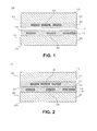
- FIG. 1 is a cross-section diagram illustrating one example of first and second device wafers that may be included in an example integrated circuit system accordance with the teachings of the present invention.
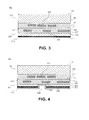
- FIG. 2 is a cross-section diagram illustrating one example of first and second device wafers that are stacked and bonded together in an example integrated circuit system accordance with the teachings of the present invention.
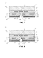
- FIG. 3 is a cross-section diagram illustrating one example of stacked and bonded first and second device wafers with one of the wafers having a thinned and passivated semiconductor layer in an example integrated circuit system accordance with the teachings of the present invention.
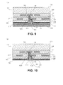
- FIG. 4 is a cross-section diagram illustrating one example of stacked and bonded first and second device wafers with an oxide deposition over an etched opening through the of one of the semiconductor layers in an example integrated circuit system accordance with the teachings of the present invention.
- FIG. 5A is a cross-section diagram illustrating one example of stacked and bonded first and second device wafers with a trench etched with a first mask in an opening through one of the semiconductor layers to a conductor in an example integrated circuit system accordance with the teachings of the present invention.
- FIG. 5B is a cross-section diagram illustrating one example of stacked and bonded first and second device wafers with a cavity etched in the trench with a second mask between first and second conductors and etched through a bonding interface and through one of the semiconductor layers from a backside of one of the device wafers in an example integrated circuit system accordance with the teachings of the present invention.
- FIG. 6A is a cross-section diagram illustrating another example of stacked and bonded first and second device wafers with a cavity etched with a first mask between first and second conductors and etched through a bonding interface and through one of the semiconductor layers from a backside of one of the device wafers in an example integrated circuit system accordance with the teachings of the present invention.
- FIG. 6B is a cross-section diagram illustrating another example of stacked and bonded first and second device wafers with a trench etched over the cavity with a second mask in an opening through one of the semiconductor layers to a conductor in an example integrated circuit system accordance with the teachings of the present invention.
- FIG. 7 is a cross-section diagram illustrating yet another example of stacked and bonded first and second device wafers with a cavity etched with a single mask between first and second conductors and etched through a donut hole in one of the conductors, through a bonding interface and through one of the semiconductor layers from a backside of one of the device wafers in an example integrated circuit system accordance with the teachings of the present invention.
- FIG. 8 is a cross-section diagram illustrating one example of stacked and bonded first and second device wafers with a barrier metal deposition over the backside and a cavity etched between first and second conductors from a backside of one of the device wafers in an example integrated circuit system accordance with the teachings of the present invention.
- FIG. 9 is a cross-section diagram illustrating one example of stacked and bonded first and second device wafers with a cavity etched between first and second conductors from a backside of one of the device wafers filled with conductive material to provide a conductive path between the first and second conductors in an example integrated circuit system accordance with the teachings of the present invention.
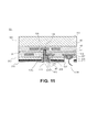
- FIG. 10 is a cross-section diagram illustrating one example of stacked and bonded first and second device wafers with the conductive material providing the conductive path between the first and second conductors etched and polished in an example integrated circuit system accordance with the teachings of the present invention.
- FIG. 11 is a cross-section diagram illustrating one example of stacked and bonded first and second device wafers with a wire bond cavity and wire bond in an example integrated circuit system accordance with the teachings of the present invention.
- FIG. 1 is a cross-section diagram illustrating one example of a first device wafer 103 and a second device wafer 203 that are included in one example of an integrated circuit system 101 in accordance with the teachings of the present invention.
- one of first device wafer 103 and second device wafer 203 may be an imager chip, an application specific integrated circuit, or the like
- the other one of first device wafer 103 and second device wafer 203 may be a processing chip, an application specific integrated circuit, or the like.
- first device wafer 103 includes a first semiconductor layer 105 proximate to a first metal layer including a first conductor 109 disposed within a first metal layer oxide 107.
- first metal layer oxide 107 is proximate to a frontside 111 of first device wafer 103 and first semiconductor layer 105 is proximate to a backside 113 of first device wafer 103.
- first semiconductor layer 105 includes silicon.
- second device wafer 203 includes a second semiconductor layer 205 proximate to a second metal layer including a second conductor 209 disposed within a second metal layer oxide 207.
- second metal layer oxide 207 is proximate to a frontside 211 of second device wafer 203 and second semiconductor layer 205 is proximate to a backside 213 of second device wafer 203.
- second semiconductor layer 205 includes silicon.
- At least one of frontside 111 of first metal layer oxide 107 and frontside 211 of the second metal layer oxide 207 is flattened by a chemical mechanical polish.
- FIG. 2 is a cross-section diagram that illustrates integrated circuit system 101 with first device wafer 103 bonded to second device wafer 203.
- frontside 111 of the first metal layer oxide 107 of the first device wafer 103 is bonded to frontside 211 of the second metal layer oxide 207 of the second device wafer 203 at a bonding interface 315 between first metal layer oxide 107 and second metal layer oxide 207 in accordance with the teachings of the present invention.
- bonding interface 315 includes an oxide-to-oxide bonding between first metal layer oxide 107 and second metal layer oxide 207.
- bonding interface 315 may be an oxide-to-conductor interface.
- at least one of the surfaces at bonding interface 315 includes the oxide of first metal layer oxide 107 and/or second metal layer oxide 207 in accordance with the teachings of the present invention. Therefore, in one example, bonding interface 315 is an oxide bonding interface in accordance with the teachings of the present invention.
- FIG. 3 is a cross-section diagram that illustrates an example of integrated circuit system 101 with stacked and bonded first device wafer 103 and second device wafer 203 as discussed above, and with second device wafer 203 having a thinned second semiconductor layer 205.
- second semiconductor layer 205 is then passivated as shown to form a passivation layer 417 on thinned second semiconductor layer 205 in accordance with the teachings of the present invention.
- FIG. 4 is a cross-section diagram that illustrates an example of integrated circuit system 101 with stacked and bonded first device wafer 103 and second device wafer 203, and second semiconductor layer 205 thinned and passivated as discussed above.
- the example depicted in FIG. 4 shows an opening 519 etched from backside 213 of second device wafer 203 through second semiconductor layer 205.
- opening 519 is etched from backside 213 through second semiconductor layer 205 to second metal layer oxide 207 as shown.
- FIG. 4 also shows that after opening 519 is etched through second semiconductor layer 205 to second metal layer oxide 207, an oxide deposition 521 is deposited on backside 213 and over opening 519 of second device wafer 203 as shown.
- FIG. 5A is a cross-section diagram illustrating one example of an example of integrated circuit system 101 with etched opening 519 through second semiconductor layer 205 covered with oxide deposition 521 as discussed above in FIGs. 1-4 .
- FIG. 5A illustrates an example in which a trench 623 is then etched in opening 519 from backside 213 through oxide deposition 521 and through second metal layer oxide 207 to second conductor 209 as shown.
- trench 623 is etched as described from backside 213 using a first mask.
- FIG. 5B continues from the example depicted above in FIG. 5A in which trench 623 is etched in opening 519 from backside 213 through oxide deposition 521 and through second metal layer oxide 207 to second conductor 209.
- a cavity 725 is then etched through trench 623 from backside 213 of the second semiconductor layer 205 and through bonding interface 315 to first conductor 109 within first metal layer oxide 107 as shown in accordance with the teachings of the present invention.
- cavity 725 is etched as described from backside 213 using a second mask.
- FIG. 6A is a cross-section diagram illustrating another example of an example of integrated circuit system 101 with etched opening 519 through second semiconductor layer 205 covered with oxide deposition 521 as discussed above in FIGs. 1-4 .
- FIG. 6A illustrates an example in which cavity 725 is etched in opening 519 from backside 213 through oxide deposition 521, through second metal layer oxide 207 and through bonding interface 315 to first conductor 109 within first metal layer oxide 107 as shown.
- cavity 725 is etched as described from backside 213 using a first mask.
- FIG. 6B continues from the example depicted above in FIG. 6A in which cavity 725 is etched in opening 519 from backside 213 through oxide deposition 521 and through second metal layer oxide 207 to first conductor 109 within first metal layer oxide 107.
- trench 623 is then etched over cavity 725 from backside 213 through oxide deposition 521 and through second metal layer oxide 207 to second conductor 209 as shown in accordance with the teachings of the present invention.
- trench 623 is etched as described from backside 213 using a second mask.
- FIG. 7 is a cross-section diagram illustrating still another example of an example of integrated circuit system 101 with etched opening 519 through second semiconductor layer 205 covered with oxide deposition 521 as discussed above in FIGs. 1-4 .
- second conductor 209 includes a donut hole 829 or other suitable opening through which a cavity can be etched.
- a cavity 827 is etched in opening 519 from backside 213 through oxide deposition 521, through second metal layer oxide 207, through donut hole 829 of second conductor 209 and through bonding interface 315 to first conductor 109 within first metal layer oxide 107 as shown.
- cavity 827 is etched as described from backside 213 using a single mask.
- FIG. 8 is a cross-section diagram that illustrates an example of integrated circuit system 101 as described in the examples above in which a cavity is etched between first conductor 109 and second conductor 209 from backside 213 through oxide deposition 521, through second metal layer oxide 207 and through bonding interface 315.
- FIG. 8 illustrates a barrier metal deposition 931 deposited from backside 213 over oxide deposition 521 and over the walls of trench 623, and cavity 725 covering exposed portions of first conductor 109, second conductor 209, first metal layer oxide 107 and second metal layer oxide 207 in accordance with the teachings of the present invention.
- FIG. 9 is a cross-section diagram that continues with the example integrated circuit system 101 as described above in which barrier metal deposition 931 is deposited from backside 213 over oxide deposition 521 and over the walls of trench 623 and cavity 725.
- FIG. 9 illustrates that cavity 725, trench 623 and opening 519 are filled from backside 213 with a conductive material 1033.
- a conductive path 1035 coupling first conductor 109 and second conductor 209 is now provided with conductive material 1033 formed in cavity 725 in accordance with the teachings of the present invention.
- first conductor 109 is coupled to second conductor 209 through conductive path 1035 and through barrier metal deposition 931.
- FIG. 10 is a cross-section diagram that continues with the example integrated circuit system 101 as described above in which cavity 725, trench 623 and opening 519 are filled with conductive material 1033 from backside 213 to provide conductive path 1035 between first conductor 109 and second conductor 209.
- FIG. 10 shows an example of backside 213 of second device wafer 203 after being etched and/or polished down to oxide deposition 521 as shown, which removes excess conductive material 1033 from backside 213 in accordance with the teachings of the present invention.
- FIG. 11 is a cross-section diagram that continues with the example integrated circuit system 101 as described above in which backside 213 of second device wafer 203 is etched and/or polished down to oxide deposition 521 removing excess conductive material 1033 from backside 213.
- FIG. 11 illustrates an example in which a wire bond cavity 1137 and a wire bond 1139 are formed to provide a package connection to a conductor in second metal layer oxide 207 in an example integrated circuit system 101 in accordance with the teachings of the present invention.
Landscapes
- Internal Circuitry In Semiconductor Integrated Circuit Devices (AREA)
Abstract
Description
- The present invention relates generally semiconductor processing. More specifically, embodiments of the present invention are related to semiconductor processing of stacked integrated circuit systems.
- As integrated circuit technologies continue to advance, there are continuing efforts to increase performance and density, improve form factor, and reduce costs. The implementation of stacked three dimensional integrated circuits have been one approach that designers sometimes use to realize these benefits. Some examples of where three dimensional integrated circuits are a suitable consideration include stacking memory on top of image sensors or processor chips, stacking memory on top of processor chips, stacking processor chips on top of image sensors, stacking chips that are fabricated with different fabrication processes, stacking two small integrated circuit chips whose separate yield may be higher than one large one, or stacking chips to reduce the integrated circuit system footprint.
- A key challenge to implementing stacked three dimensional integrated circuits is how to make many small area interconnects between the integrated circuit chips with high yield and reliability. For example, the typical copper-to-copper bonds between the stacked integrated circuit chips often suffer from wafer warpage as well as bow. Furthermore, the copper surface roughness and non-planarity present additional challenges when trying to provide connections between the integrated circuit chips. Other known techniques for making the many small area interconnects between the stacked integrated circuit chips are also expensive, unreliable and large.
- Non-limiting and non-exhaustive embodiments of the present invention are described with reference to the following figures, wherein like reference numerals refer to like parts throughout the various views unless otherwise specified.
-
FIG. 1 is a cross-section diagram illustrating one example of first and second device wafers that may be included in an example integrated circuit system accordance with the teachings of the present invention. -
FIG. 2 is a cross-section diagram illustrating one example of first and second device wafers that are stacked and bonded together in an example integrated circuit system accordance with the teachings of the present invention. -
FIG. 3 is a cross-section diagram illustrating one example of stacked and bonded first and second device wafers with one of the wafers having a thinned and passivated semiconductor layer in an example integrated circuit system accordance with the teachings of the present invention. -
FIG. 4 is a cross-section diagram illustrating one example of stacked and bonded first and second device wafers with an oxide deposition over an etched opening through the of one of the semiconductor layers in an example integrated circuit system accordance with the teachings of the present invention. -
FIG. 5A is a cross-section diagram illustrating one example of stacked and bonded first and second device wafers with a trench etched with a first mask in an opening through one of the semiconductor layers to a conductor in an example integrated circuit system accordance with the teachings of the present invention. -
FIG. 5B is a cross-section diagram illustrating one example of stacked and bonded first and second device wafers with a cavity etched in the trench with a second mask between first and second conductors and etched through a bonding interface and through one of the semiconductor layers from a backside of one of the device wafers in an example integrated circuit system accordance with the teachings of the present invention. -
FIG. 6A is a cross-section diagram illustrating another example of stacked and bonded first and second device wafers with a cavity etched with a first mask between first and second conductors and etched through a bonding interface and through one of the semiconductor layers from a backside of one of the device wafers in an example integrated circuit system accordance with the teachings of the present invention. -
FIG. 6B is a cross-section diagram illustrating another example of stacked and bonded first and second device wafers with a trench etched over the cavity with a second mask in an opening through one of the semiconductor layers to a conductor in an example integrated circuit system accordance with the teachings of the present invention. -
FIG. 7 is a cross-section diagram illustrating yet another example of stacked and bonded first and second device wafers with a cavity etched with a single mask between first and second conductors and etched through a donut hole in one of the conductors, through a bonding interface and through one of the semiconductor layers from a backside of one of the device wafers in an example integrated circuit system accordance with the teachings of the present invention. -
FIG. 8 is a cross-section diagram illustrating one example of stacked and bonded first and second device wafers with a barrier metal deposition over the backside and a cavity etched between first and second conductors from a backside of one of the device wafers in an example integrated circuit system accordance with the teachings of the present invention. -
FIG. 9 is a cross-section diagram illustrating one example of stacked and bonded first and second device wafers with a cavity etched between first and second conductors from a backside of one of the device wafers filled with conductive material to provide a conductive path between the first and second conductors in an example integrated circuit system accordance with the teachings of the present invention. -
FIG. 10 is a cross-section diagram illustrating one example of stacked and bonded first and second device wafers with the conductive material providing the conductive path between the first and second conductors etched and polished in an example integrated circuit system accordance with the teachings of the present invention. -
FIG. 11 is a cross-section diagram illustrating one example of stacked and bonded first and second device wafers with a wire bond cavity and wire bond in an example integrated circuit system accordance with the teachings of the present invention. - As will be shown, examples of a method and apparatus providing an integrated circuit system with stacked integrated circuit device wafers using one or more conductive paths between conductors in respective metal layer oxides through a bonding interface are disclosed. In the following description, numerous specific details are set forth in order to provide a thorough understanding of the present invention. It will be apparent, however, to one having ordinary skill in the art that the specific detail need not be employed to practice the present invention. In other instances, well-known materials or methods have not been described in detail in order to avoid obscuring the present invention.
- Reference throughout this specification to "one embodiment", "an embodiment", "one example" or "an example" means that a particular feature, structure or characteristic described in connection with the embodiment or example is included in at least one embodiment of the present invention. Thus, appearances of the phrases "in one embodiment", "in an embodiment", "one example" or "an example" in various places throughout this specification are not necessarily all referring to the same embodiment or example. Furthermore, the particular features, structures or characteristics may be combined in any suitable combinations and/or subcombinations in one or more embodiments or examples. Particular features, structures or characteristics may be included in an integrated circuit, an electronic circuit, a combinational logic circuit, or other suitable components that provide the described functionality. In addition, it is appreciated that the figures provided herewith are for explanation purposes to persons ordinarily skilled in the art and that the drawings are not necessarily drawn to scale.
- To illustrate,
FIG. 1 is a cross-section diagram illustrating one example of afirst device wafer 103 and asecond device wafer 203 that are included in one example of an integratedcircuit system 101 in accordance with the teachings of the present invention. In one example, one of first device wafer 103 andsecond device wafer 203 may be an imager chip, an application specific integrated circuit, or the like, and the other one offirst device wafer 103 andsecond device wafer 203 may be a processing chip, an application specific integrated circuit, or the like. - As shown in the example,
first device wafer 103 includes afirst semiconductor layer 105 proximate to a first metal layer including afirst conductor 109 disposed within a firstmetal layer oxide 107. In the depicted example, firstmetal layer oxide 107 is proximate to afrontside 111 offirst device wafer 103 andfirst semiconductor layer 105 is proximate to abackside 113 offirst device wafer 103. In one example,first semiconductor layer 105 includes silicon. - Continuing with the example depicted in
FIG. 1 ,second device wafer 203 includes asecond semiconductor layer 205 proximate to a second metal layer including asecond conductor 209 disposed within a secondmetal layer oxide 207. In the depicted example, secondmetal layer oxide 207 is proximate to afrontside 211 ofsecond device wafer 203 andsecond semiconductor layer 205 is proximate to abackside 213 ofsecond device wafer 203. In one example,second semiconductor layer 205 includes silicon. - In one example, at least one of
frontside 111 of firstmetal layer oxide 107 andfrontside 211 of the secondmetal layer oxide 207 is flattened by a chemical mechanical polish. -
FIG. 2 is a cross-section diagram that illustratesintegrated circuit system 101 with first device wafer 103 bonded tosecond device wafer 203. As shown in the depicted example,frontside 111 of the firstmetal layer oxide 107 of thefirst device wafer 103 is bonded tofrontside 211 of the secondmetal layer oxide 207 of the second device wafer 203 at abonding interface 315 between firstmetal layer oxide 107 and secondmetal layer oxide 207 in accordance with the teachings of the present invention. - In the example illustrated in
FIG. 2 , it is noted that all of the conductors includingfirst conductor 109 of the first metal layer within firstmetal layer oxide 107 are illustrated beneath thefrontside 111 surface offirst device wafer 103. Similarly, it is noted that all of the conductors includingsecond conductor 209 of the second metal layer within secondmetal layer oxide 207 are illustrated beneath thefrontside 211 surface ofsecond device wafer 203. Therefore, in the depicted example,bonding interface 315 includes an oxide-to-oxide bonding between firstmetal layer oxide 107 and secondmetal layer oxide 207. In another example, it is appreciated that if one of the metal layers includes conductors that are flush with surface offrontside 111 orfrontside 211, then thebonding interface 315 may be an oxide-to-conductor interface. However, in either example, at least one of the surfaces atbonding interface 315 includes the oxide of firstmetal layer oxide 107 and/or secondmetal layer oxide 207 in accordance with the teachings of the present invention. Therefore, in one example,bonding interface 315 is an oxide bonding interface in accordance with the teachings of the present invention. -
FIG. 3 is a cross-section diagram that illustrates an example ofintegrated circuit system 101 with stacked and bondedfirst device wafer 103 andsecond device wafer 203 as discussed above, and with second device wafer 203 having a thinnedsecond semiconductor layer 205. In one example, aftersecond semiconductor layer 205 is thinned frombackside 213 as illustrated,second semiconductor layer 205 is then passivated as shown to form apassivation layer 417 on thinnedsecond semiconductor layer 205 in accordance with the teachings of the present invention. -
FIG. 4 is a cross-section diagram that illustrates an example ofintegrated circuit system 101 with stacked and bonded first device wafer 103 andsecond device wafer 203, andsecond semiconductor layer 205 thinned and passivated as discussed above. In addition, the example depicted inFIG. 4 shows anopening 519 etched frombackside 213 of second device wafer 203 throughsecond semiconductor layer 205. In one example, opening 519 is etched frombackside 213 throughsecond semiconductor layer 205 to secondmetal layer oxide 207 as shown. - Continuing with the illustrated example,
FIG. 4 also shows that after opening 519 is etched throughsecond semiconductor layer 205 to secondmetal layer oxide 207, anoxide deposition 521 is deposited onbackside 213 and over opening 519 ofsecond device wafer 203 as shown. -
FIG. 5A is a cross-section diagram illustrating one example of an example ofintegrated circuit system 101 withetched opening 519 throughsecond semiconductor layer 205 covered withoxide deposition 521 as discussed above inFIGs. 1-4 . In addition,FIG. 5A illustrates an example in which atrench 623 is then etched in opening 519 frombackside 213 throughoxide deposition 521 and through secondmetal layer oxide 207 tosecond conductor 209 as shown. In one example,trench 623 is etched as described frombackside 213 using a first mask. -
FIG. 5B continues from the example depicted above inFIG. 5A in whichtrench 623 is etched in opening 519 frombackside 213 throughoxide deposition 521 and through secondmetal layer oxide 207 tosecond conductor 209. In the example depicted inFIG. 5B , acavity 725 is then etched throughtrench 623 frombackside 213 of thesecond semiconductor layer 205 and throughbonding interface 315 tofirst conductor 109 within firstmetal layer oxide 107 as shown in accordance with the teachings of the present invention. In one example,cavity 725 is etched as described frombackside 213 using a second mask. -
FIG. 6A is a cross-section diagram illustrating another example of an example ofintegrated circuit system 101 with etchedopening 519 throughsecond semiconductor layer 205 covered withoxide deposition 521 as discussed above inFIGs. 1-4 . In addition,FIG. 6A illustrates an example in whichcavity 725 is etched in opening 519 frombackside 213 throughoxide deposition 521, through secondmetal layer oxide 207 and throughbonding interface 315 tofirst conductor 109 within firstmetal layer oxide 107 as shown. In one example,cavity 725 is etched as described frombackside 213 using a first mask. -
FIG. 6B continues from the example depicted above inFIG. 6A in whichcavity 725 is etched in opening 519 frombackside 213 throughoxide deposition 521 and through secondmetal layer oxide 207 tofirst conductor 109 within firstmetal layer oxide 107. In the example depicted inFIG. 6B ,trench 623 is then etched overcavity 725 frombackside 213 throughoxide deposition 521 and through secondmetal layer oxide 207 tosecond conductor 209 as shown in accordance with the teachings of the present invention. In one example,trench 623 is etched as described frombackside 213 using a second mask. -
FIG. 7 is a cross-section diagram illustrating still another example of an example ofintegrated circuit system 101 with etchedopening 519 throughsecond semiconductor layer 205 covered withoxide deposition 521 as discussed above inFIGs. 1-4 . In addition,FIG. 7 illustrates an example in whichsecond conductor 209 includes adonut hole 829 or other suitable opening through which a cavity can be etched. For instance, in the example depicted inFIG. 7 , acavity 827 is etched in opening 519 frombackside 213 throughoxide deposition 521, through secondmetal layer oxide 207, throughdonut hole 829 ofsecond conductor 209 and throughbonding interface 315 tofirst conductor 109 within firstmetal layer oxide 107 as shown. In one example,cavity 827 is etched as described frombackside 213 using a single mask. -
FIG. 8 is a cross-section diagram that illustrates an example ofintegrated circuit system 101 as described in the examples above in which a cavity is etched betweenfirst conductor 109 andsecond conductor 209 frombackside 213 throughoxide deposition 521, through secondmetal layer oxide 207 and throughbonding interface 315. In addition,FIG. 8 illustrates abarrier metal deposition 931 deposited frombackside 213 overoxide deposition 521 and over the walls oftrench 623, andcavity 725 covering exposed portions offirst conductor 109,second conductor 209, firstmetal layer oxide 107 and secondmetal layer oxide 207 in accordance with the teachings of the present invention. -
FIG. 9 is a cross-section diagram that continues with the example integratedcircuit system 101 as described above in whichbarrier metal deposition 931 is deposited frombackside 213 overoxide deposition 521 and over the walls oftrench 623 andcavity 725. In addition,FIG. 9 illustrates thatcavity 725,trench 623 andopening 519 are filled frombackside 213 with aconductive material 1033. Accordingly, aconductive path 1035 couplingfirst conductor 109 andsecond conductor 209 is now provided withconductive material 1033 formed incavity 725 in accordance with the teachings of the present invention. Thus,first conductor 109 is coupled tosecond conductor 209 throughconductive path 1035 and throughbarrier metal deposition 931. -
FIG. 10 is a cross-section diagram that continues with the example integratedcircuit system 101 as described above in whichcavity 725,trench 623 andopening 519 are filled withconductive material 1033 frombackside 213 to provideconductive path 1035 betweenfirst conductor 109 andsecond conductor 209. In addition,FIG. 10 shows an example ofbackside 213 ofsecond device wafer 203 after being etched and/or polished down tooxide deposition 521 as shown, which removes excessconductive material 1033 frombackside 213 in accordance with the teachings of the present invention. -
FIG. 11 is a cross-section diagram that continues with the example integratedcircuit system 101 as described above in whichbackside 213 ofsecond device wafer 203 is etched and/or polished down tooxide deposition 521 removing excessconductive material 1033 frombackside 213. In addition,FIG. 11 illustrates an example in which awire bond cavity 1137 and awire bond 1139 are formed to provide a package connection to a conductor in secondmetal layer oxide 207 in an example integratedcircuit system 101 in accordance with the teachings of the present invention. - The above description of illustrated examples of the present invention, including what is described in the Abstract, are not intended to be exhaustive or to be limitation to the precise forms disclosed. While specific embodiments of, and examples for, the invention are described herein for illustrative purposes, various equivalent modifications are possible without departing from the broader spirit and scope of the present invention. Indeed, it is appreciated that the specific example voltages, currents, frequencies, power range values, times, etc., are provided for explanation purposes and that other values may also be employed in other embodiments and examples in accordance with the teachings of the present invention.
- These modifications can be made to examples of the invention in light of the above detailed description. The terms used in the following claims should not be construed to limit the invention to the specific embodiments disclosed in the specification and the claims. Rather, the scope is to be determined entirely by the following claims, which are to be construed in accordance with established doctrines of claim interpretation. The present specification and figures are accordingly to be regarded as illustrative rather than restrictive.
Claims (15)
- An integrated circuit system, comprising:a first device wafer having a first semiconductor layer proximate to a first metal layer including a first conductor disposed within a first metal layer oxide;a second device wafer having a second semiconductor layer proximate to a second metal layer including a second conductor disposed within a second metal layer oxide, wherein a front side of the first metal layer oxide of the first device wafer is bonded to a front side of the second metal layer oxide of the second device wafer at a bonding interface between the first metal layer oxide and the second metal layer oxide; anda conductive path coupling the first conductor to the second conductor, wherein the conductive path is provided with conductive material formed in a cavity etched between the first conductor and the second conductor and etched through the bonding interface and through the second semiconductor layer from a backside of the second device wafer.
- The integrated circuit system of claim 1 further comprising a barrier metal deposition deposited in the cavity between the conductive path and the first conductor and the second conductor, wherein the first conductor is coupled to the second conductor through the barrier metal deposition and the conductive path.
- The integrated circuit system of any of the above claims further comprising an oxide deposition disposed between the conductive material and the second semiconductor layer.
- The integrated circuit system of claim 3 further comprising a passivation layer disposed between the backside of the second semiconductor layer and the oxide deposition.
- The integrated circuit system of any of the above claims wherein at least one of the front side of the first metal layer oxide and the front side of the second metal layer oxide is flattened by a chemical mechanical polish.
- A method of fabricating an integrated circuit system, comprising
forming a first conductor in a first metal layer disposed within a first metal layer oxide proximate to a first semiconductor layer of a first device wafer;
forming a second conductor in a second metal layer disposed within a second metal layer oxide proximate to a second semiconductor layer of a second device wafer;
bonding a frontside of the first metal layer oxide of the first device wafer to a frontside of the second metal layer oxide of the second device wafer at a bonding interface between the first metal layer oxide and the second metal layer oxide;
etching a cavity between the first conductor and the second conductor and through the bonding interface and through the second semiconductor layer from a backside of the second device wafer; and
filling the cavity with conductive material to provide a conductive path coupling the first conductor to the second conductor. - The method of claim 6 further comprising depositing a barrier metal deposition in the cavity prior to filling the cavity with the conductive material to provide the conductive path coupling the first conductor to the second conductor.
- The method of claim 6 or 7 further comprising passivating the backside of the second device wafer prior to etching the cavity between the first conductor and the second conductor.
- The method of any of claims 6-8 further comprising depositing an oxide deposition on the backside of the second device wafer prior to etching the cavity between the first conductor and the second conductor.
- The method of any of claims 6-9further comprising flattening at least one of the frontside of the first metal layer oxide and the frontside of the second metal layer oxide by chemical mechanical polishing prior to bonding the frontside of the first metal layer oxide of the first device wafer to the frontside of the second metal layer oxide of the second device wafer.
- The integrated circuit system of any of any of claims 1-5 or the method of any of claims 6-10 wherein the second semiconductor layer through which the cavity is etched is thinned prior to etching of the cavity.
- The integrated circuit system of any of claims 1-5 or 11 or the method of any of claims 6-11 wherein the cavity is further etched through a donut hole in the second conductor.
- The integrated circuit system of any of claims 1-5 or 11-12 or the method of any of claims 6-12 wherein the cavity is further etched through a trench etched from the backside of the second semiconductor layer to the first conductor.
- The integrated circuit system of any of claims 1-5 or 11-13 or the method of any of claims 6-13 wherein the cavity is etched prior to etching the trench from the backside of the second semiconductor layer to the first conductor.
- The integrated circuit system of any of claims 1-5 or 11-14 or the method of any of claims 6-14 wherein one of the first device wafer and second device wafer comprises an imager chip and another one of the first device wafer and second device wafer comprises a processing chip.
Applications Claiming Priority (1)
| Application Number | Priority Date | Filing Date | Title |
|---|---|---|---|
| US13/441,627 US20130264688A1 (en) | 2012-04-06 | 2012-04-06 | Method and apparatus providing integrated circuit system with interconnected stacked device wafers |
Publications (2)
| Publication Number | Publication Date |
|---|---|
| EP2648215A2 true EP2648215A2 (en) | 2013-10-09 |
| EP2648215A3 EP2648215A3 (en) | 2017-01-18 |
Family
ID=48095565
Family Applications (1)
| Application Number | Title | Priority Date | Filing Date |
|---|---|---|---|
| EP13161771.4A Withdrawn EP2648215A3 (en) | 2012-04-06 | 2013-03-28 | Method and apparatus providing integrated circuit system with interconnected stacked device wafers |
Country Status (5)
| Country | Link |
|---|---|
| US (1) | US20130264688A1 (en) |
| EP (1) | EP2648215A3 (en) |
| KR (1) | KR20130114000A (en) |
| CN (1) | CN103367348A (en) |
| TW (1) | TW201349428A (en) |
Cited By (3)
| Publication number | Priority date | Publication date | Assignee | Title |
|---|---|---|---|---|
| CN105977222A (en) * | 2016-06-15 | 2016-09-28 | 苏州晶方半导体科技股份有限公司 | Semiconductor chip packaging structure and packaging method |
| US11031833B2 (en) | 2013-11-06 | 2021-06-08 | Sony Corporation | Solid-state imaging device, method of manufacturing solid-state imaging device, and electronic apparatus |
| EP4131374A4 (en) * | 2020-04-17 | 2023-05-31 | Huawei Technologies Co., Ltd. | SEMI-CONDUCTOR STRUCTURE AND METHOD OF MANUFACTURING IT |
Families Citing this family (33)
| Publication number | Priority date | Publication date | Assignee | Title |
|---|---|---|---|---|
| US9293418B2 (en) * | 2007-07-03 | 2016-03-22 | Taiwan Semiconductor Manufacturing Company, Ltd. | Backside through vias in a bonded structure |
| US9214435B2 (en) * | 2012-05-21 | 2015-12-15 | Globalfoundries Inc. | Via structure for three-dimensional circuit integration |
| US8933544B2 (en) * | 2012-07-12 | 2015-01-13 | Omnivision Technologies, Inc. | Integrated circuit stack with integrated electromagnetic interference shielding |
| US9076715B2 (en) * | 2013-03-12 | 2015-07-07 | Taiwan Semiconductor Manufacturing Company, Ltd. | Interconnect structure for connecting dies and methods of forming the same |
| US20150187701A1 (en) | 2013-03-12 | 2015-07-02 | Taiwan Semiconductor Manufacturing Company, Ltd. | Semiconductor Devices and Methods of Manufacture Thereof |
| US9536777B2 (en) | 2013-03-13 | 2017-01-03 | Taiwan Semiconductor Manufacutring Company, Ltd. | Interconnect apparatus and method |
| US9764153B2 (en) * | 2013-03-14 | 2017-09-19 | Taiwan Semiconductor Manufacturing Company, Ltd. | Interconnect structure and method of forming same |
| US10096515B2 (en) | 2013-03-15 | 2018-10-09 | Taiwan Semiconductor Manufacturing Company, Ltd. | Interconnect structure for stacked device |
| US9356066B2 (en) | 2013-03-15 | 2016-05-31 | Taiwan Semiconductor Manufacturing Company, Ltd. | Interconnect structure for stacked device and method |
| CN104051419B (en) * | 2013-03-15 | 2017-06-06 | 台湾积体电路制造股份有限公司 | For the interconnection structure of stack device |
| US9293392B2 (en) * | 2013-09-06 | 2016-03-22 | Taiwan Semiconductor Manufacturing Company, Ltd. | 3DIC interconnect apparatus and method |
| US9412719B2 (en) * | 2013-12-19 | 2016-08-09 | Taiwan Semiconductor Manufacturing Company, Ltd. | 3DIC interconnect apparatus and method |
| US10056353B2 (en) | 2013-12-19 | 2018-08-21 | Taiwan Semiconductor Manufacturing Company, Ltd. | 3DIC interconnect apparatus and method |
| US9425150B2 (en) * | 2014-02-13 | 2016-08-23 | Taiwan Semiconductor Manufacturing Company, Ltd. | Multi-via interconnect structure and method of manufacture |
| US9679936B2 (en) * | 2014-02-27 | 2017-06-13 | Semiconductor Components Industries, Llc | Imaging systems with through-oxide via connections |
| US9543257B2 (en) * | 2014-05-29 | 2017-01-10 | Taiwan Semiconductor Manufacturing Company, Ltd. | 3DIC interconnect devices and methods of forming same |
| US9455158B2 (en) | 2014-05-30 | 2016-09-27 | Taiwan Semiconductor Manufacturing Company, Ltd. | 3DIC interconnect devices and methods of forming same |
| US9449914B2 (en) | 2014-07-17 | 2016-09-20 | Taiwan Semiconductor Manufacturing Company, Ltd. | Stacked integrated circuits with redistribution lines |
| CN104377164A (en) * | 2014-09-28 | 2015-02-25 | 武汉新芯集成电路制造有限公司 | Through silicon var wafer interconnection process |
| US9343499B1 (en) * | 2015-04-23 | 2016-05-17 | Omnivision Technologies, Inc. | Integrated circuit stack with strengthened wafer bonding |
| TWI604565B (en) * | 2015-08-04 | 2017-11-01 | 精材科技股份有限公司 | Sensing chip package and manufacturing method thereof |
| CN106611756A (en) * | 2015-10-26 | 2017-05-03 | 联华电子股份有限公司 | Wafer-to-wafer butting structure and manufacturing method thereof |
| JP2017204510A (en) * | 2016-05-09 | 2017-11-16 | キヤノン株式会社 | Method of manufacturing photoelectric conversion device |
| FR3057392A1 (en) * | 2016-10-11 | 2018-04-13 | Stmicroelectronics (Crolles 2) Sas | INTEGRATED CIRCUIT CHIP REINFORCED FOR FRONT-SIDE ATTACKS |
| US10026687B1 (en) | 2017-02-20 | 2018-07-17 | Globalfoundries Inc. | Metal interconnects for super (skip) via integration |
| CN108155198B (en) * | 2017-12-22 | 2021-04-02 | 成都先锋材料有限公司 | A CMOS image sensor package structure and manufacturing method thereof |
| CN107946335B (en) * | 2017-12-22 | 2020-10-27 | 成都先锋材料有限公司 | CMOS image sensing packaging structure and manufacturing method thereof |
| CN110858597B (en) * | 2018-08-22 | 2022-03-11 | 中芯国际集成电路制造(天津)有限公司 | Method for forming through silicon via structure, method for forming CIS wafer, and CIS wafer |
| CN109166840B (en) * | 2018-08-28 | 2019-07-23 | 武汉新芯集成电路制造有限公司 | Polycrystalline circle stacked structure and forming method thereof |
| KR102887940B1 (en) | 2020-08-13 | 2025-11-17 | 삼성전자 주식회사 | Integrated circuit device |
| US20220406956A1 (en) * | 2021-06-22 | 2022-12-22 | Texas Instruments Incorporated | Integrated circuit with a galvanically-isolated commuincation channel using a back-side etched channel |
| US11830865B2 (en) * | 2021-10-26 | 2023-11-28 | Nanya Technology Corporation | Semiconductor device with redistribution structure and method for fabricating the same |
| US20230130354A1 (en) * | 2021-10-27 | 2023-04-27 | Advanced Micro Devices, Inc. | Three-dimensional semiconductor package having a stacked passive device |
Family Cites Families (10)
| Publication number | Priority date | Publication date | Assignee | Title |
|---|---|---|---|---|
| US7453150B1 (en) * | 2004-04-01 | 2008-11-18 | Rensselaer Polytechnic Institute | Three-dimensional face-to-face integration assembly |
| KR100830581B1 (en) * | 2006-11-06 | 2008-05-22 | 삼성전자주식회사 | A semiconductor device having a through electrode and a method of forming the semiconductor device |
| US7855455B2 (en) * | 2008-09-26 | 2010-12-21 | International Business Machines Corporation | Lock and key through-via method for wafer level 3 D integration and structures produced |
| JP5985136B2 (en) * | 2009-03-19 | 2016-09-06 | ソニー株式会社 | SEMICONDUCTOR DEVICE, ITS MANUFACTURING METHOD, AND ELECTRONIC DEVICE |
| US8344478B2 (en) * | 2009-10-23 | 2013-01-01 | Maxim Integrated Products, Inc. | Inductors having inductor axis parallel to substrate surface |
| US8399180B2 (en) * | 2010-01-14 | 2013-03-19 | International Business Machines Corporation | Three dimensional integration with through silicon vias having multiple diameters |
| US8415238B2 (en) * | 2010-01-14 | 2013-04-09 | International Business Machines Corporation | Three dimensional integration and methods of through silicon via creation |
| US8143712B2 (en) * | 2010-07-15 | 2012-03-27 | Nanya Technology Corp. | Die package structure |
| KR20120031811A (en) * | 2010-09-27 | 2012-04-04 | 삼성전자주식회사 | Semiconductor devices and methods of fabricating the same |
| JP2012094720A (en) * | 2010-10-27 | 2012-05-17 | Sony Corp | Solid state image pick up device, semiconductor device, method for manufacturing solid state image pick up device and semiconductor device, and electronic apparatus |
-
2012
- 2012-04-06 US US13/441,627 patent/US20130264688A1/en not_active Abandoned
- 2012-09-18 CN CN2012103476186A patent/CN103367348A/en active Pending
-
2013
- 2013-03-28 EP EP13161771.4A patent/EP2648215A3/en not_active Withdrawn
- 2013-04-03 TW TW102112222A patent/TW201349428A/en unknown
- 2013-04-04 KR KR20130037058A patent/KR20130114000A/en not_active Ceased
Non-Patent Citations (1)
| Title |
|---|
| None |
Cited By (5)
| Publication number | Priority date | Publication date | Assignee | Title |
|---|---|---|---|---|
| US11031833B2 (en) | 2013-11-06 | 2021-06-08 | Sony Corporation | Solid-state imaging device, method of manufacturing solid-state imaging device, and electronic apparatus |
| US11689070B2 (en) | 2013-11-06 | 2023-06-27 | Sony Group Corporation | Solid-state imaging device, method of manufacturing solid-state imaging device, and electronic apparatus |
| CN105977222A (en) * | 2016-06-15 | 2016-09-28 | 苏州晶方半导体科技股份有限公司 | Semiconductor chip packaging structure and packaging method |
| CN105977222B (en) * | 2016-06-15 | 2019-09-17 | 苏州晶方半导体科技股份有限公司 | Semiconductor chip package and packaging method |
| EP4131374A4 (en) * | 2020-04-17 | 2023-05-31 | Huawei Technologies Co., Ltd. | SEMI-CONDUCTOR STRUCTURE AND METHOD OF MANUFACTURING IT |
Also Published As
| Publication number | Publication date |
|---|---|
| EP2648215A3 (en) | 2017-01-18 |
| CN103367348A (en) | 2013-10-23 |
| KR20130114000A (en) | 2013-10-16 |
| TW201349428A (en) | 2013-12-01 |
| US20130264688A1 (en) | 2013-10-10 |
Similar Documents
| Publication | Publication Date | Title |
|---|---|---|
| US20130264688A1 (en) | Method and apparatus providing integrated circuit system with interconnected stacked device wafers | |
| EP1851797B1 (en) | Device and method for fabricating double-sided soi wafer scale package with through via connections | |
| US10930619B2 (en) | Multi-wafer bonding structure and bonding method | |
| CN214672598U (en) | Three-dimensional semiconductor device structure and three-dimensional semiconductor device | |
| US8378462B2 (en) | Semiconductor device having through substrate vias | |
| US9536809B2 (en) | Combination of TSV and back side wiring in 3D integration | |
| US20090042365A1 (en) | Three-dimensional face-to-face integration assembly | |
| US8906781B2 (en) | Method for electrically connecting wafers using butting contact structure and semiconductor device fabricated through the same | |
| CN101335261A (en) | Stacked integrated circuits and semiconductor devices | |
| JP2011258687A (en) | Semiconductor device and method of manufacturing the same | |
| CN112349736A (en) | Semiconductor device structure and manufacturing method thereof | |
| CN109166840B (en) | Polycrystalline circle stacked structure and forming method thereof | |
| TW201919133A (en) | Method of manufacturing semiconductor package structure | |
| CN111244057A (en) | Bonding structure and manufacturing method thereof | |
| US20180190571A1 (en) | Semiconductor device having through-silicon-via and methods of forming the same | |
| CN103219303B (en) | The encapsulating structure of a kind of TSV back side small opening and method | |
| CN101853778A (en) | Method and system for stacking and aligning multiple integrated circuits | |
| CN102881666B (en) | wafer level device package | |
| CN110112168A (en) | Stack imaging sensor and forming method thereof | |
| JP7657747B2 (en) | Semiconductor Device | |
| CN112530899B (en) | Semiconductor device and method for manufacturing the same | |
| CN103247569A (en) | Fabrication method and structure of through-silicon vias | |
| HK1188331A (en) | Method and apparatus providing integrated circuit system with interconnected stacked device wafers | |
| US20260047176A1 (en) | Semiconductor device and method of fabricating the same | |
| JP6662015B2 (en) | Semiconductor device and method of manufacturing semiconductor device |
Legal Events
| Date | Code | Title | Description |
|---|---|---|---|
| PUAI | Public reference made under article 153(3) epc to a published international application that has entered the european phase |
Free format text: ORIGINAL CODE: 0009012 |
|
| AK | Designated contracting states |
Kind code of ref document: A2 Designated state(s): AL AT BE BG CH CY CZ DE DK EE ES FI FR GB GR HR HU IE IS IT LI LT LU LV MC MK MT NL NO PL PT RO RS SE SI SK SM TR |
|
| AX | Request for extension of the european patent |
Extension state: BA ME |
|
| PUAL | Search report despatched |
Free format text: ORIGINAL CODE: 0009013 |
|
| AK | Designated contracting states |
Kind code of ref document: A3 Designated state(s): AL AT BE BG CH CY CZ DE DK EE ES FI FR GB GR HR HU IE IS IT LI LT LU LV MC MK MT NL NO PL PT RO RS SE SI SK SM TR |
|
| AX | Request for extension of the european patent |
Extension state: BA ME |
|
| RIC1 | Information provided on ipc code assigned before grant |
Ipc: H01L 21/60 20060101ALN20161214BHEP Ipc: H01L 23/48 20060101ALI20161214BHEP Ipc: H01L 23/00 20060101AFI20161214BHEP Ipc: H01L 27/146 20060101ALN20161214BHEP Ipc: H01L 25/065 20060101ALI20161214BHEP Ipc: H01L 21/768 20060101ALI20161214BHEP |
|
| STAA | Information on the status of an ep patent application or granted ep patent |
Free format text: STATUS: THE APPLICATION IS DEEMED TO BE WITHDRAWN |
|
| 18D | Application deemed to be withdrawn |
Effective date: 20170719 |