EP2645419A2 - ROM arrays having memory cell transistors programmed using metal gates - Google Patents
ROM arrays having memory cell transistors programmed using metal gates Download PDFInfo
- Publication number
- EP2645419A2 EP2645419A2 EP12006387.0A EP12006387A EP2645419A2 EP 2645419 A2 EP2645419 A2 EP 2645419A2 EP 12006387 A EP12006387 A EP 12006387A EP 2645419 A2 EP2645419 A2 EP 2645419A2
- Authority
- EP
- European Patent Office
- Prior art keywords
- memory cell
- metal gate
- cell transistor
- metal
- transistor
- Prior art date
- Legal status (The legal status is an assumption and is not a legal conclusion. Google has not performed a legal analysis and makes no representation as to the accuracy of the status listed.)
- Withdrawn
Links
Images





Classifications
-
- H—ELECTRICITY
- H10—SEMICONDUCTOR DEVICES; ELECTRIC SOLID-STATE DEVICES NOT OTHERWISE PROVIDED FOR
- H10D—INORGANIC ELECTRIC SEMICONDUCTOR DEVICES
- H10D84/00—Integrated devices formed in or on semiconductor substrates that comprise only semiconducting layers, e.g. on Si wafers or on GaAs-on-Si wafers
- H10D84/80—Integrated devices formed in or on semiconductor substrates that comprise only semiconducting layers, e.g. on Si wafers or on GaAs-on-Si wafers characterised by the integration of at least one component covered by groups H10D12/00 or H10D30/00, e.g. integration of IGFETs
- H10D84/82—Integrated devices formed in or on semiconductor substrates that comprise only semiconducting layers, e.g. on Si wafers or on GaAs-on-Si wafers characterised by the integration of at least one component covered by groups H10D12/00 or H10D30/00, e.g. integration of IGFETs of only field-effect components
-
- H—ELECTRICITY
- H10—SEMICONDUCTOR DEVICES; ELECTRIC SOLID-STATE DEVICES NOT OTHERWISE PROVIDED FOR
- H10B—ELECTRONIC MEMORY DEVICES
- H10B20/00—Read-only memory [ROM] devices
- H10B20/27—ROM only
- H10B20/30—ROM only having the source region and the drain region on the same level, e.g. lateral transistors
- H10B20/36—Gate programmed, e.g. different gate material or no gate
-
- H—ELECTRICITY
- H10—SEMICONDUCTOR DEVICES; ELECTRIC SOLID-STATE DEVICES NOT OTHERWISE PROVIDED FOR
- H10B—ELECTRONIC MEMORY DEVICES
- H10B20/00—Read-only memory [ROM] devices
- H10B20/60—Peripheral circuit regions
- H10B20/65—Peripheral circuit regions of memory structures of the ROM only type
-
- H—ELECTRICITY
- H10—SEMICONDUCTOR DEVICES; ELECTRIC SOLID-STATE DEVICES NOT OTHERWISE PROVIDED FOR
- H10D—INORGANIC ELECTRIC SEMICONDUCTOR DEVICES
- H10D30/00—Field-effect transistors [FET]
- H10D30/01—Manufacture or treatment
- H10D30/021—Manufacture or treatment of FETs having insulated gates [IGFET]
- H10D30/0212—Manufacture or treatment of FETs having insulated gates [IGFET] using self-aligned silicidation
-
- H—ELECTRICITY
- H10—SEMICONDUCTOR DEVICES; ELECTRIC SOLID-STATE DEVICES NOT OTHERWISE PROVIDED FOR
- H10D—INORGANIC ELECTRIC SEMICONDUCTOR DEVICES
- H10D64/00—Electrodes of devices having potential barriers
- H10D64/01—Manufacture or treatment
- H10D64/017—Manufacture or treatment using dummy gates in processes wherein at least parts of the final gates are self-aligned to the dummy gates, i.e. replacement gate processes
-
- H—ELECTRICITY
- H10—SEMICONDUCTOR DEVICES; ELECTRIC SOLID-STATE DEVICES NOT OTHERWISE PROVIDED FOR
- H10D—INORGANIC ELECTRIC SEMICONDUCTOR DEVICES
- H10D64/00—Electrodes of devices having potential barriers
- H10D64/60—Electrodes characterised by their materials
- H10D64/66—Electrodes having a conductor capacitively coupled to a semiconductor by an insulator, e.g. MIS electrodes
- H10D64/665—Electrodes having a conductor capacitively coupled to a semiconductor by an insulator, e.g. MIS electrodes the conductor comprising a layer of elemental metal contacting the insulator, e.g. tungsten or molybdenum
- H10D64/666—Electrodes having a conductor capacitively coupled to a semiconductor by an insulator, e.g. MIS electrodes the conductor comprising a layer of elemental metal contacting the insulator, e.g. tungsten or molybdenum the conductor further comprising additional layers
-
- H—ELECTRICITY
- H10—SEMICONDUCTOR DEVICES; ELECTRIC SOLID-STATE DEVICES NOT OTHERWISE PROVIDED FOR
- H10D—INORGANIC ELECTRIC SEMICONDUCTOR DEVICES
- H10D64/00—Electrodes of devices having potential barriers
- H10D64/60—Electrodes characterised by their materials
- H10D64/66—Electrodes having a conductor capacitively coupled to a semiconductor by an insulator, e.g. MIS electrodes
- H10D64/68—Electrodes having a conductor capacitively coupled to a semiconductor by an insulator, e.g. MIS electrodes characterised by the insulator, e.g. by the gate insulator
- H10D64/691—Electrodes having a conductor capacitively coupled to a semiconductor by an insulator, e.g. MIS electrodes characterised by the insulator, e.g. by the gate insulator comprising metallic compounds, e.g. metal oxides or metal silicates
-
- H—ELECTRICITY
- H10—SEMICONDUCTOR DEVICES; ELECTRIC SOLID-STATE DEVICES NOT OTHERWISE PROVIDED FOR
- H10D—INORGANIC ELECTRIC SEMICONDUCTOR DEVICES
- H10D64/00—Electrodes of devices having potential barriers
- H10D64/01—Manufacture or treatment
- H10D64/013—Manufacture or treatment of electrodes having a conductor capacitively coupled to a semiconductor by an insulator
- H10D64/01302—Manufacture or treatment of electrodes having a conductor capacitively coupled to a semiconductor by an insulator the insulator being formed after the semiconductor body, the semiconductor being silicon
- H10D64/01304—Manufacture or treatment of electrodes having a conductor capacitively coupled to a semiconductor by an insulator the insulator being formed after the semiconductor body, the semiconductor being silicon characterised by the conductor
- H10D64/01316—Manufacture or treatment of electrodes having a conductor capacitively coupled to a semiconductor by an insulator the insulator being formed after the semiconductor body, the semiconductor being silicon characterised by the conductor the conductor comprising a layer of elemental metal contacting the insulator, e.g. Ta, W, Mo or Al
-
- H—ELECTRICITY
- H10—SEMICONDUCTOR DEVICES; ELECTRIC SOLID-STATE DEVICES NOT OTHERWISE PROVIDED FOR
- H10D—INORGANIC ELECTRIC SEMICONDUCTOR DEVICES
- H10D64/00—Electrodes of devices having potential barriers
- H10D64/01—Manufacture or treatment
- H10D64/013—Manufacture or treatment of electrodes having a conductor capacitively coupled to a semiconductor by an insulator
- H10D64/01302—Manufacture or treatment of electrodes having a conductor capacitively coupled to a semiconductor by an insulator the insulator being formed after the semiconductor body, the semiconductor being silicon
- H10D64/01304—Manufacture or treatment of electrodes having a conductor capacitively coupled to a semiconductor by an insulator the insulator being formed after the semiconductor body, the semiconductor being silicon characterised by the conductor
- H10D64/01318—Manufacture or treatment of electrodes having a conductor capacitively coupled to a semiconductor by an insulator the insulator being formed after the semiconductor body, the semiconductor being silicon characterised by the conductor the conductor comprising a layer of alloy material, compound material or organic material contacting the insulator, e.g. TiN
-
- H—ELECTRICITY
- H10—SEMICONDUCTOR DEVICES; ELECTRIC SOLID-STATE DEVICES NOT OTHERWISE PROVIDED FOR
- H10D—INORGANIC ELECTRIC SEMICONDUCTOR DEVICES
- H10D64/00—Electrodes of devices having potential barriers
- H10D64/60—Electrodes characterised by their materials
- H10D64/66—Electrodes having a conductor capacitively coupled to a semiconductor by an insulator, e.g. MIS electrodes
- H10D64/667—Electrodes having a conductor capacitively coupled to a semiconductor by an insulator, e.g. MIS electrodes the conductor comprising a layer of alloy material, compound material or organic material contacting the insulator, e.g. TiN workfunction layers
-
- H—ELECTRICITY
- H10—SEMICONDUCTOR DEVICES; ELECTRIC SOLID-STATE DEVICES NOT OTHERWISE PROVIDED FOR
- H10D—INORGANIC ELECTRIC SEMICONDUCTOR DEVICES
- H10D64/00—Electrodes of devices having potential barriers
- H10D64/60—Electrodes characterised by their materials
- H10D64/66—Electrodes having a conductor capacitively coupled to a semiconductor by an insulator, e.g. MIS electrodes
- H10D64/667—Electrodes having a conductor capacitively coupled to a semiconductor by an insulator, e.g. MIS electrodes the conductor comprising a layer of alloy material, compound material or organic material contacting the insulator, e.g. TiN workfunction layers
- H10D64/669—Electrodes having a conductor capacitively coupled to a semiconductor by an insulator, e.g. MIS electrodes the conductor comprising a layer of alloy material, compound material or organic material contacting the insulator, e.g. TiN workfunction layers the conductor further comprising additional layers of alloy material, compound material or organic material, e.g. TaN/TiAlN
Definitions
- ROM Read-only memory
- IC integrated circuit
- ROM is typically structured as an array of memory cell transistors, and is usually programmed with data during manufacture. By programming the array such that some memory cell transistors are distinguishable from others by sensing circuitry on the IC, logical states corresponding to binary data are stored on the ROM.
- ROM programming Various techniques are known for ROM programming.
- One approach is to utilize a high-grade interconnect mask to block contact to some of the memory cell transistors.
- Another approach is to use a channel implant to alter a threshold voltage of some of the memory cell transistors, providing a detectable threshold voltage difference.
- gate oxides of different thickness may provide different threshold voltages for the memory cell transistors.
- the present disclosure is directed to ROM arrays having memory cell transistors programmed using metal gates, substantially as shown in and/or described in connection with at least one of the figures, and as set forth more completely in the claims.
- an integrated circuit comprising:
- said first memory cell transistor and said second memory cell transistor are of a first conductivity type.
- said first memory cell transistor includes a first high-k gate dielectric and said second memory cell transistor includes a second high-k gate dielectric.
- the IC further comprises an overlying gate segment situated over said first metal gate of said first memory cell transistor.
- said overlying gate segment is of said second work function.
- the IC further comprises a first logic transistor, said first logic transistor having a third metal gate of said first work function and having a third threshold voltage.
- said first memory cell transistor is of a first conductivity type and said first logic transistor is of a second conductivity type.
- the IC further comprises a second logic transistor, said second logic transistor having a fourth metal gate of said second work function and having a fourth threshold voltage.
- a method for fabricating an integrated circuit comprises:
- said first memory cell transistor and said second memory cell transistor are of a first conductivity type.
- the method further comprises forming a metal fill layer over said second metal gate layer.
- the method further comprises forming, from said first metal gate layer, a third metal gate of a first logic transistor, said third metal gate of said first work function and having a third threshold voltage.
- said first memory cell transistor is of a first conductivity type and said first logic transistor is of a second conductivity type.
- the method further comprises forming, from said second metal gate layer, a fourth metal gate of a second logic transistor, said fourth metal gate of said second work function and having a fourth threshold voltage.
- the method further comprises utilizing a same implant to form source/drain regions of said first and second memory cell transistors.
- said first memory cell transistor includes a first high-k gate dielectric and said second memory cell transistor includes a second high-k gate dielectric.
- a method for fabricating an integrated circuit comprises:
- the method further comprises forming, from said first metal gate layer, a third metal gate of a first P type logic transistor, said third metal gate of said first work function and having a third threshold voltage.
- the method further comprises forming, from said second metal gate layer, a fourth metal gate of a second P type logic transistor, said fourth metal gate of said second work function and having a fourth threshold voltage.
- the method further comprises forming a metal fill layer over said second metal gate layer.
- Figure 1 shows a process flow diagram illustrating an exemplary process for fabricating an integrated circuit (IC). More particularly, Figure 1 shows a process flow diagram illustrating a process 100 for fabricating an integrated circuit (IC). While applicable for fabricating various ICs shown and described in this disclosure, for illustrative purposes, the process 100 is described with respect to the structures shown in Figures 2A , 2B , 2C , 2D , 2E , 2F , and 2G and the IC shown in Figure 3 .
- the implementation illustrated by the process 100 can be performed on a processed wafer, which includes, among other things, a substrate, such as a silicon substrate, conductive wells (P type or N type) for channel regions in the substrate, and isolation regions, such as shallow trench isolation (STI) regions.
- a substrate such as a silicon substrate
- conductive wells P type or N type
- isolation regions such as shallow trench isolation (STI) regions.
- the wafer may also be referred to as a semiconductor die or simply a die.
- the process 100 includes forming a poly segment (e.g., 212a, 212b) over a dielectric segment (e.g., 210a, 210b) and a cap segment (e.g., 214a, 214b) over the poly segment in first (e.g., 204a) and second (e.g., 204b) memory cell regions of a substrate (e.g., 206) (170).
- a structure 270 includes a memory cell region 204a and a memory cell region 204b (also referred to as "memory cell regions 204") of a substrate 206.
- the structure 270 also includes a logic region 204c and a logic region 204d (also referred to as "logic regions 204") of the substrate 206.
- the memory cell regions 204 and the logic regions 204 are also referred to collectively as substrate regions 204.
- the substrate 206 is a semiconductor substrate, and more particularly, a silicon substrate.
- the substrate 206 can include other materials in addition to or instead of silicon.
- the substrate 206 includes isolation regions 208a, 208b, 208c, 208d, and 208e (also referred to as "isolation regions 208"), which can be shallow trench isolation (STI) regions or other types of isolation regions.
- the isolation regions 208 can include silicon oxide or other dielectric material.
- Various ones of the isolation regions 208 are shown as being in more than one of the memory cell regions 204 and/or the logic regions 204 for simplicity. However, specific depicted locations of the isolation regions 208 are not intended to be limiting.
- the memory cell regions 204 are designated for memory cell transistor formation in the substrate 206.
- the logic regions 204 are designated for logic transistor formation in the substrate 206.
- any combination of the substrate regions 204 can be designated for memory cell transistor formation or logic transistor formation.
- all of the substrate regions 204 may be designated for memory cell transistor formation, or all of the substrate regions 204 may be designated for logic transistor formation.
- aspects of the present disclosure are not limited to memory cell transistor formation and logic transistor formation.
- the substrate regions 204 respectively include dielectric segments 210a, 210b, 210c, and 210d (also referred to as “dielectric segments 210"), poly segments 212a, 212b, 212c, and 212d (also referred to as “poly segments 212"), and cap segments 214a, 214b, 214c, and 214d (also referred to as "cap segments 214").
- the structure 270 corresponds to an exemplary implementation after forming the poly segments 212 over the dielectric segments 210 and the cap segments 214 over the poly segments 212 in the substrate regions 204.
- the poly segments 212 are formed respectively over the dielectric segments 210 and the cap segments 214 are formed respectively over the poly segments 212 in the memory cell regions 204a and 204b.
- the poly segments 212 are formed respectively over the dielectric segments 210 and the cap segments 214 are formed respectively over the poly segments 212 in the logic regions 204c and 204d.
- the dielectric segments 210 include high-k dielectric material. Suitable materials for the dielectric segments 210 include, as specific examples, hafnium oxide (HfO 2 ), zirconium oxide (ZrO 2 ), chromium oxide (CrO 2 ), and the like. However, in some implementations, the dielectric segments 210 include silicon oxide, silicon nitride, and/or other types of dielectric materials instead of or in addition to high-k dielectric material. While in some implementations the dielectric segments 210 include substantially similar materials, in other implementations the dielectric segments 210 include different materials with respect to one another. Similarly, the poly segments 212 and the cap segments 214 may have different materials with respect to one another.
- forming the dielectric segments 210, the poly segments 212, and the cap segments 214 includes sequentially forming a dielectric layer, a poly layer, and a cap layer on the substrate 206.
- the dielectric layer and the cap layer can be formed respectively by depositing dielectric material over the substrate 206 utilizing physical vapor deposition (PVD), chemical vapor deposition (CVD), or another deposition technique.
- the poly layer can be formed by depositing a layer of polysilicon over the substrate 206 utilizing PVD, CVD, or another deposition technique.
- the dielectric layer, the poly layer, and the cap layer can be patterned to form the dielectric segments 210, the poly segments 212, and the cap segments 214.
- the patterning which can include masking and etching, may expose a top surface 202 of the substrate 206.
- the patterning can also define gate lengths 223a, 223b, 223c, and 223d for memory cell transistors and logic transistors to be formed in the substrate regions 204.
- the gate lengths 223a, 223b, 223c, and 223d are less than or equal to approximately 20 nm.
- the process 100 includes forming sources (e.g., 220a, 220b), drains (e.g., 220a, 220b), spacers (e.g., 216a, 216b), and silicide segments (e.g., 218a, 218b) in first (e.g., 204a) and second (e.g., 204b) memory cell regions (172).
- sources e.g., 220a, 220b
- drains e.g., 220a, 220b
- spacers e.g., 216a, 216b
- silicide segments e.g., 218a, 218b
- a structure 272 includes spacers 216a, 216b, 216c, and 216d (also referred to as “spacers 216"), silicide segments 218a, 218b, 218c, and 218d (also referred to as “silicide segments 218"), and source/drain regions 220a, 220b, 220c, and 220d (also referred to as “source/drains 220").
- the structure 272 corresponds to an exemplary implementation after forming sources/drains 220, the spacers 216, and the silicide segments 218 in the substrate regions 204.
- the spacers 216 are formed adjacent to and respectively surround the dielectric segments 210, the poly segments 212, and the cap segments 214.
- the spacers 216 can include silicon oxide and/or other dielectric material.
- the spacers 216 can be formed by conformally depositing a layer of dielectric material, such as silicon oxide, over the substrate 206 and the cap segments 214 of the structure 270. The deposition can be accomplished utilizing CVD or another type of deposition and appropriately performing an etch-back of the layer of dielectric material.
- the source/drain regions 220 are formed in the substrate 206 adjacent to and respectively under the dielectric segments 210.
- the source/drain regions 220 can be formed by implanting dopants into the substrate 206 and performing an implant anneal to diffuse the dopants in the substrate 206.
- Each of the source/drain regions 220 can be formed utilizing the same or different dopant types and/or concentrations.
- any combination of the source/drain regions 220 can be P type or N type.
- the source/drain regions 220a and 220b are of a first conductivity type, or N type
- the source/drain regions 220c and 220d are of a second conductivity type, or P type.
- the source/drain regions 220a and 220b may be formed utilizing a same implant and anneal and may have a substantially same doping profile.
- the source/drain regions 220c and 220d may be formed utilizing a same implant and anneal and may have a substantially same doping profile.
- the silicide segments 218 are formed respectively on the source/drain regions 220 and are respectively adjacent to the dielectric segments 210.
- the silicide segments 218 can include metal silicide such as copper silicide, nickel silicide, nickel-platinum silicide or cobalt silicide.
- the cap segments 214 prevent silicidation of the poly segments 212 during formation of the silicide segments 218.
- the process 100 includes forming an interlayer dielectric (e.g., 222) between the spacers (e.g., 216a, 216b) and removing the cap segments (e.g., 214a, 214b) and the poly segments (e.g., 212a, 212b) from the first (e.g., 204a) and second (e.g., 204b) memory cell regions (174).
- a structure 274 corresponds to an exemplary implementation after forming an interlayer dielectric 222 between the spacers 216 and removing the cap segments 214 and the poly segments 212 from the substrate regions 204.
- the interlayer dielectric 222 is formed on and surrounds the spacers 216.
- the interlayer dielectric 222 includes dielectric material, and in the present implementation, is a nitride. In other implementations, the interlayer dielectric 222 can include an oxide or other dielectric material.
- the interlayer dielectric 222 can be formed by depositing dielectric material over the substrate 206 and the cap segments 214 of the structure 272. The deposition can utilize PVD, CVD, or another deposition technique. The deposited dielectric material can then be planarized utilizing chemical mechanical planarization (CMP) or another planarization technique.
- CMP chemical mechanical planarization
- the cap segments 214 can be removed, for example utilizing a selective etch, such as an oxide selective etch, or another type of etch to expose the poly segments 212. Utilizing a selective etch, the cap segments 214 can be removed without removing the interlayer dielectric 222 (e.g. where the interlayer dielectric 222 is a nitride and the cap segments 214 are oxide).
- the poly segments 212 can also be removed, for example utilizing a selective etch, or another type of etch to expose the dielectric segments 210.
- a selective etch may remove the poly segments 212 without removing the dielectric segments 210. This can be useful in implementations where it is desirable to have a controlled thickness of the dielectric segments 210.
- One such implementation is where the dielectric segments 210 are subsequently included in gate dielectrics of memory cell and/or logic transistors in the substrate regions 204.
- the dielectric segments 210 remain in the substrate regions 204 and are utilized as gate dielectrics for memory cell and logic transistors to be formed in the substrate regions 204.
- at least one of the dielectric segments 210 can be removed in other implementations, which may include utilizing a selective etch.
- one or more other dielectric materials can optionally be deposited and utilized for gate dielectrics of memory cell and/or logic transistors to be formed in the substrate regions 204.
- the process 100 includes forming a first metal gate layer (e.g., 224) in the first (e.g., 204a) and second (e.g., 204b) memory cell regions (176).
- a structure 276 corresponds to an exemplary implementation after forming a metal gate layer 224 in the substrate regions 204.
- the metal gate layer 224 includes metal for a gate of a high-k metal gate transistor, such as an N type high-k metal gate transistor. Suitable materials for an N type high-k metal gate transistor include, as specific examples, tantalum (Ta), tantalum nitride (TaN), titanium nitride (TiN), or other metal or metal stack. In other implementations, the metal gate layer 224 includes metal for a gate of a P type high-k metal gate transistor, or other types of transistors including non-high-k metal gate transistors.
- the metal gate layer 224 can be formed by depositing a layer of metal over the dielectric segments 210 of the structure 274. The deposition can utilize PVD, CVD, or another deposition technique.
- the process 100 includes forming, from the first metal gate layer (e.g., 224), a first metal gate (e.g., 224a) of a first memory cell transistor (e.g., 234a), the first metal gate of a first work function (e.g., f 1 ), the first memory cell transistor having a first threshold voltage (e.g., Vt 1 ) (178).
- a structure 278 corresponds to an exemplary implementation after forming, from the metal gate layer 224, a metal gate 224a of a memory cell transistor 234a in Figure 2G .
- the metal gate 224a is of a work function f 1 and the memory cell transistor 234a has a threshold voltage Vt 1 .
- the present implementation includes optionally forming, from the metal gate layer 224, a metal gate 224b of a logic transistor 234c in Figure 2G .
- the metal gate 224b is of the work function f 1 and the logic transistor 234c has a threshold voltage Vt 3 .
- the memory cell transistor 234a is of a first conductivity type and the logic transistor 234c is of a second conductivity type.
- the metal gates 224a and 224b can both be formed from the metal gate layer 224 while the logic transistor 234c has the threshold voltage Vt 3 , which is different than the threshold voltage Vt 1 of the memory cell transistor 234a.
- the metal gates 224a and 224b can be formed by masking and etching the metal gate layer 224.
- a mask 226, shown in Figure 2E is formed over the structure 276 in Figure 2D and the metal gate layer 224 is etched to form the metal gates 224a and 224b.
- the mask 226 covers at least a portion of the metal gate layer 224 over the dielectric segments 210a and 210c and exposes the metal gate layer 224 over the dielectric segments 210b and 210d.
- the exposed portions of the metal gate layer 224 over the dielectric segments 210b and 210d are removed during etching.
- the metal gates 224a and 224b can be approximately 10 nm to approximately 30 nm thick.
- the process 100 includes forming a second metal gate layer (e.g., 228) and optionally a metal fill layer (e.g., 230) over the second gate layer in the first (e.g., 204a) and second (e.g., 204b) memory cell regions (180).
- a structure 280 corresponds to an implementation after forming a metal gate layer 228, and forming a metal fill layer 230 over the metal gate layer 228 in the substrate regions 204.
- the metal gate layer 228 includes metal for a gate of a high-k metal gate transistor, such as a P type high-k metal gate transistor. Suitable materials for the P type high-k metal gate transistor include, as specific examples, molybdenum (Mo), ruthenium (Ru), tantalum carbide nitride (TaCN), or other metal or metal stack. In other implementations, the metal gate layer 228 includes metal for a gate of a N type high-k metal gate transistor, or other types of transistors including non-high-k metal gate transistors.
- the metal gate layer 228 can be formed by depositing a layer of metal over the dielectric segments 210 of Figure 2E . The layer of metal can be deposited utilizing PVD, CVD, or another deposition technique.
- the metal fill layer 230 is formed over the metal gate layer 228.
- the metal fill layer 230 can include metals of lower resistivity than the metal gate layers 224 and 228.
- the metal fill layer 230 can be used to provide low resistance contact to memory cell and logic transistors to be formed in the substrate regions 204.
- Examples of metals for the metal fill layer 230 include aluminum and copper.
- the metal fill layer 230 can be formed by depositing a layer of metal over the metal gate layer 228.
- the process 100 includes forming, from the second metal gate layer (e.g., 228), a second metal gate (e.g., 228b) of a second memory cell transistor (e.g., 234b), the second metal gate of a second work function (e.g., f 2 ), the second memory cell transistor having a second threshold voltage (e.g., Vt 2 ) (182).
- a structure 282 corresponds to an exemplary implementation after forming, from the metal gate layer 228, a metal gate 228b of a memory cell transistor 234b.
- the metal gate 228b is of a work function f 2 and the memory cell transistor 234b has a threshold voltage Vt 2 .
- the present implementation includes optionally forming, from the metal gate layer 228, a metal gate 228d of a logic transistor 234d.
- the metal gate 228d is of the work function f 2 and the logic transistor 234d has a threshold voltage Vt 4 .
- the memory cell transistor 234b is of a first conductivity type and the logic transistor 234d is of a second conductivity type.
- the metal gates 228b and 228d can both be formed from the metal gate layer 228 while the logic transistor 234d has the threshold voltage Vt 4 , which is different than the threshold voltage Vt 2 of the memory cell transistor 234b.
- the metal gates 228b and 228d can be formed from the metal gate layer 228 by performing a CMP or another type of planarization on the structure 280 in Figure 2F .
- the metal gates 228b and 228d can be approximately 10 nm to approximately 30 nm thick. Additional processing can be performed to provide the memory cell transistors 234a and 234b and the logic transistors 234c and 234d (also referred to collectively as "transistors 234") in Figure 2G . This may include formation of contacts for the transistors 234.
- the memory cell transistor 234a includes the metal gate 224a of the work function f 1 and having the threshold voltage V t1 .
- the memory cell transistor 234a also optionally includes an overlying gate segment 228a (including gate metal) formed from the metal gate layer 228 and situated over the metal gate 224a.
- the overlying gate segment 228a can be approximately 10 nm to approximately 30 nm thick.
- the memory cell transistor 234a optionally includes a metal fill 230a formed from the metal fill layer 230.
- the memory cell transistor 234b includes the metal gate 228b of the work function f 2 and having the threshold voltage V t2 .
- the memory cell transistor 234b also optionally includes a metal fill 230b formed from the metal fill layer 230.
- the metal gate layer 224 includes metal for a gate of an N type high-k metal gate transistor and the metal gate layer 228 includes metal for a gate of a P type high-k metal gate transistor. This results in the threshold voltage V t2 being greater than the threshold voltage V t1 .
- the logic transistor 234c includes the metal gate 224b of the work function f 1 and having the threshold voltage V t3 .
- the logic transistor 234c also optionally includes an overlying gate segment 228c (including gate metal) formed from the metal gate layer 228 and situated over the metal gate 224b.
- the overlying gate segment 228c can be approximately 10 nm to approximately 30 nm thick.
- the logic transistor 234c optionally includes a metal fill 230c formed from the metal fill layer 230.
- the logic transistor 234d includes the metal gate 228d of the work function f 2 and having the threshold voltage V t4 .
- the logic transistor 234d also optionally includes a metal fill 230d formed from the metal fill layer 230.
- the metal gate layer 224 includes metal for a gate of an N type high-k metal gate transistor and the metal gate layer 228 includes metal for a gate of a P type high-k metal gate transistor. This results in the threshold voltage V t4 being greater than the threshold voltage V t3 .
- the memory cell transistors 234a and 234b also respectively include the dielectric segments 210a and 210b, which are gate dielectrics, and in the present implementation, high-k gate dielectrics.
- the logic transistors 234c and 234d respectively include the dielectric segments 210c and 210d, which are gate dielectrics, and in the present implementation, high-k gate dielectrics.
- the dielectric segments 210 can be formed from a same dielectric layer so as to be substantially similar in thickness and composition.
- the memory cell transistors 234a and 234b are of a first conductivity type and the logic transistors 234c and 234d are of a second conductivity type.
- the memory cell transistors 234a and 234b are N type memory cell transistors respectively including a channel region 235a and a channel region 235b that are P type and the source/drain regions 220 that are N type.
- the logic transistors 234c and 234d are P type logic transistors respectively including a channel region 235c and a channel region 235d that are N type and the source/drain regions 220 that are P type.
- the memory cell transistors 234a and 234b are P type transistors and the logic transistors 234c and 234d are N type transistors.
- four different one of the transistors 234 can be fabricated utilizing only two metal gate layers 224 and 228, with each of the transistors 234 having different threshold voltages V t1 , V t2 , V t3 , and V t4 .
- Figures 2A , 2B , 2C , 2D , 2E , 2F , and 2G demonstrate formation of four different transistors 234, any combination and number of the transistors 234 may be fabricated in various implementations. For example, in some implementations, only the memory cell transistors 234a and 234b and the logic transistor 234d are fabricated.
- Figure 3 illustrates a top view of an exemplary IC including a ROM array. More particularly, Figure 3 illustrates an IC 300 including a ROM array 336.
- the ROM array 336 includes memory cell transistors 340, of which memory cell transistors 340a, 340b, and 340c are individually labeled.
- the IC 300 also includes logic transistors, of which logic transistors 342a, 342b, 342d, 342e, 342f, and 342g are shown.
- the IC 300 can be fabricated by utilizing the process 100, described above.
- the transistors 234 of Figure 2G can correspond to any of the memory cell transistors 340 and the logic transistors 342a, 342b, 342d, 342e, 342f, and 342g, or other transistors not specifically shown.
- the memory cell transistors 234a and 234b in Figure 2G correspond to any combination of the memory cell transistors 340.
- the memory cell transistors 234a and 234b can correspond to different logical states in the ROM array 336. More particularly, some of the memory cell transistors 340 are substantially similar to the memory cell transistor 234a so as to have the threshold voltage V t1 corresponding to a first logical state. Others of the memory cell transistors 340 are substantially similar to the memory cell transistor 234b so as to have the threshold voltage V t2 corresponding to a second logical state.
- the IC 300 is configured to sense the first and second logical states based on the threshold voltages V t1 and V t2 .
- the threshold voltages V t1 and V t2 differ by at least approximately 100 mV. In some implementations, the threshold voltages V t1 and V t2 differ by approximately 200 mV to approximately 400 mV.
- the ROM array 336 can be programmed utilizing the memory cell transistors 234a and 234b including the metal gates 224a and 228b with different work functions f 1 and f 2 .
- the ROM array 336 can have highly secure programming that is difficult to reverse engineer. More particularly, physical differences between the memory cell transistors 234a and 234b may not be readily apparent. Thus, it can be difficult to reverse engineer programming of the ROM array 336 utilizing visual inspection or other non-invasive means.
- the ROM array 336 can easily and inexpensively be fabricated with different programming by altering the mask 226, which is a low grade mask.
- the memory cell transistor 234a and the memory cell transistor 234b can have the source/drain regions 220 and the channel regions 235a and 235b be functionally interchangeable (e.g. due to being formed using the same implant and anneal).
- the dielectric segments 210, serving as gate dielectrics can be functionally interchangeable (e.g. due to being fabricated from the same dielectric layer).
- the memory cell transistor 234a in Figure 2G can be made to have the threshold voltage V t2 simply by changing the mask 226 so that the overlying gate segment 228a forms a metal gate of the memory cell transistor 234a.
- the memory cell transistor 234b in Figure 2G can be made to have the threshold voltage V t1 simply by changing the mask 226 so that the overlying gate segment 228c forms a metal gate of the memory cell transistor 234a.
Landscapes
- Semiconductor Memories (AREA)
- Metal-Oxide And Bipolar Metal-Oxide Semiconductor Integrated Circuits (AREA)
Abstract
Description
- Read-only memory (ROM) is often utilized to store data, such as firmware data, on an integrated circuit (IC). ROM is typically structured as an array of memory cell transistors, and is usually programmed with data during manufacture. By programming the array such that some memory cell transistors are distinguishable from others by sensing circuitry on the IC, logical states corresponding to binary data are stored on the ROM.
- Various techniques are known for ROM programming. One approach is to utilize a high-grade interconnect mask to block contact to some of the memory cell transistors. Another approach is to use a channel implant to alter a threshold voltage of some of the memory cell transistors, providing a detectable threshold voltage difference. In yet another approach, gate oxides of different thickness may provide different threshold voltages for the memory cell transistors.
- The present disclosure is directed to ROM arrays having memory cell transistors programmed using metal gates, substantially as shown in and/or described in connection with at least one of the figures, and as set forth more completely in the claims.
- According to an aspect, an integrated circuit (IC) is provided, comprising:
- a first memory cell transistor of a read only memory (ROM) array, said first memory cell transistor comprising a first metal gate of a first work function and having a first threshold voltage;
- a second memory cell transistor of said ROM array, said second memory cell transistor comprising a second metal gate of a second work function and having a second threshold voltage.
- Advantageously, said first memory cell transistor and said second memory cell transistor are of a first conductivity type.
- Advantageously, said first memory cell transistor includes a first high-k gate dielectric and said second memory cell transistor includes a second high-k gate dielectric.
- Advantageously, the IC further comprises an overlying gate segment situated over said first metal gate of said first memory cell transistor.
- Advantageously, said overlying gate segment is of said second work function.
- Advantageously, the IC further comprises a first logic transistor, said first logic transistor having a third metal gate of said first work function and having a third threshold voltage.
- Advantageously, said first memory cell transistor is of a first conductivity type and said first logic transistor is of a second conductivity type.
- Advantageously, the IC further comprises a second logic transistor, said second logic transistor having a fourth metal gate of said second work function and having a fourth threshold voltage.
- According to an aspect, a method for fabricating an integrated circuit (IC) comprises:
- forming, from a first metal gate layer, a first metal gate of a first memory cell transistor of a read only memory (ROM) array, said first metal gate of a first work function and having a first threshold voltage;
- forming, from a second metal gate layer, a second metal gate of a second memory cell transistor of said ROM array, said second metal gate of a second work function and having a second threshold voltage.
- Advantageously, said first memory cell transistor and said second memory cell transistor are of a first conductivity type.
- Advantageously, the method further comprises forming a metal fill layer over said second metal gate layer.
- Advantageously, the method further comprises forming, from said first metal gate layer, a third metal gate of a first logic transistor, said third metal gate of said first work function and having a third threshold voltage.
- Advantageously, said first memory cell transistor is of a first conductivity type and said first logic transistor is of a second conductivity type.
- Advantageously, the method further comprises forming, from said second metal gate layer, a fourth metal gate of a second logic transistor, said fourth metal gate of said second work function and having a fourth threshold voltage.
- Advantageously, the method further comprises utilizing a same implant to form source/drain regions of said first and second memory cell transistors.
- Advantageously, said first memory cell transistor includes a first high-k gate dielectric and said second memory cell transistor includes a second high-k gate dielectric.
- According to an aspect, a method for fabricating an integrated circuit (IC) comprises:
- forming, from a first metal gate layer, a first metal gate of a first N type memory cell transistor of a read only memory (ROM) array, said first metal gate of a first work function and having a first threshold voltage;
- forming, from a second metal gate layer, a second metal gate of a second N type memory cell transistor of said ROM array, said second metal gate of a second work function and having a second threshold voltage.
- Advantageously, the method further comprises forming, from said first metal gate layer, a third metal gate of a first P type logic transistor, said third metal gate of said first work function and having a third threshold voltage.
- Advantageously, the method further comprises forming, from said second metal gate layer, a fourth metal gate of a second P type logic transistor, said fourth metal gate of said second work function and having a fourth threshold voltage.
- Advantageously, the method further comprises forming a metal fill layer over said second metal gate layer.
-
-
Figure 1 shows a process flow diagram illustrating an exemplary process for fabricating an integrated circuit (IC). -
Figure 2A illustrates a cross-sectional view of a potion of an exemplary IC during processing. -
Figure 2B illustrates a cross-sectional view of a potion of an exemplary IC during processing. -
Figure 2C illustrates a cross-sectional view of a potion of an exemplary IC during processing. -
Figure 2D illustrates a cross-sectional view of a potion of an exemplary IC during processing. -
Figure 2E illustrates a cross-sectional view of a potion of an exemplary IC during processing. -
Figure 2F illustrates a cross-sectional view of a potion of an exemplary IC during processing. -
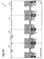
Figure 2G illustrates a cross-sectional view of a potion of an exemplary IC during processing. -
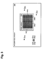
Figure 3 illustrates a top view of an exemplary IC including a ROM array. - The following description contains specific information pertaining to implementations in the present disclosure. The drawings in the present application and their accompanying detailed description are directed to merely exemplary implementations. Unless noted otherwise, like or corresponding elements among the figures may be indicated by like or corresponding reference numerals. Moreover, the drawings and illustrations in the present application are generally not to scale, and are not intended to correspond to actual relative dimensions.
-
Figure 1 shows a process flow diagram illustrating an exemplary process for fabricating an integrated circuit (IC). More particularly,Figure 1 shows a process flow diagram illustrating aprocess 100 for fabricating an integrated circuit (IC). While applicable for fabricating various ICs shown and described in this disclosure, for illustrative purposes, theprocess 100 is described with respect to the structures shown inFigures 2A ,2B ,2C ,2D ,2E ,2F , and2G and the IC shown inFigure 3 . - The implementation illustrated by the
process 100 can be performed on a processed wafer, which includes, among other things, a substrate, such as a silicon substrate, conductive wells (P type or N type) for channel regions in the substrate, and isolation regions, such as shallow trench isolation (STI) regions. The wafer may also be referred to as a semiconductor die or simply a die. - Referring now to
Figure 1 andFigure 2A , theprocess 100 includes forming a poly segment (e.g., 212a, 212b) over a dielectric segment (e.g., 210a, 210b) and a cap segment (e.g., 214a, 214b) over the poly segment in first (e.g., 204a) and second (e.g., 204b) memory cell regions of a substrate (e.g., 206) (170). Astructure 270 includes amemory cell region 204a and amemory cell region 204b (also referred to as "memory cell regions 204") of asubstrate 206. Thestructure 270 also includes alogic region 204c and alogic region 204d (also referred to as "logic regions 204") of thesubstrate 206. The memory cell regions 204 and the logic regions 204 are also referred to collectively as substrate regions 204. - In the present implementation, the
substrate 206 is a semiconductor substrate, and more particularly, a silicon substrate. However, thesubstrate 206 can include other materials in addition to or instead of silicon. Thesubstrate 206 includesisolation regions - The memory cell regions 204 are designated for memory cell transistor formation in the
substrate 206. Similarly, the logic regions 204 are designated for logic transistor formation in thesubstrate 206. However, in various implementations, any combination of the substrate regions 204 can be designated for memory cell transistor formation or logic transistor formation. For example, all of the substrate regions 204 may be designated for memory cell transistor formation, or all of the substrate regions 204 may be designated for logic transistor formation. Furthermore, aspects of the present disclosure are not limited to memory cell transistor formation and logic transistor formation. - The substrate regions 204 respectively include
dielectric segments poly segments cap segments structure 270 corresponds to an exemplary implementation after forming the poly segments 212 over the dielectric segments 210 and the cap segments 214 over the poly segments 212 in the substrate regions 204. The poly segments 212 are formed respectively over the dielectric segments 210 and the cap segments 214 are formed respectively over the poly segments 212 in thememory cell regions logic regions - The dielectric segments 210 include high-k dielectric material. Suitable materials for the dielectric segments 210 include, as specific examples, hafnium oxide (HfO2), zirconium oxide (ZrO2), chromium oxide (CrO2), and the like. However, in some implementations, the dielectric segments 210 include silicon oxide, silicon nitride, and/or other types of dielectric materials instead of or in addition to high-k dielectric material. While in some implementations the dielectric segments 210 include substantially similar materials, in other implementations the dielectric segments 210 include different materials with respect to one another. Similarly, the poly segments 212 and the cap segments 214 may have different materials with respect to one another.
- In one implementation, forming the dielectric segments 210, the poly segments 212, and the cap segments 214 includes sequentially forming a dielectric layer, a poly layer, and a cap layer on the
substrate 206. The dielectric layer and the cap layer can be formed respectively by depositing dielectric material over thesubstrate 206 utilizing physical vapor deposition (PVD), chemical vapor deposition (CVD), or another deposition technique. The poly layer can be formed by depositing a layer of polysilicon over thesubstrate 206 utilizing PVD, CVD, or another deposition technique. - Subsequently, the dielectric layer, the poly layer, and the cap layer can be patterned to form the dielectric segments 210, the poly segments 212, and the cap segments 214. The patterning, which can include masking and etching, may expose a
top surface 202 of thesubstrate 206. As will become apparent from subsequent Figures, the patterning can also definegate lengths gate lengths - Referring now to
Figure 1 andFigure 2B , theprocess 100 includes forming sources (e.g., 220a, 220b), drains (e.g., 220a, 220b), spacers (e.g., 216a, 216b), and silicide segments (e.g., 218a, 218b) in first (e.g., 204a) and second (e.g., 204b) memory cell regions (172). As shown inFigure 2B , astructure 272 includesspacers silicide segments drain regions structure 272 corresponds to an exemplary implementation after forming sources/drains 220, the spacers 216, and the silicide segments 218 in the substrate regions 204. - The spacers 216 are formed adjacent to and respectively surround the dielectric segments 210, the poly segments 212, and the cap segments 214. The spacers 216 can include silicon oxide and/or other dielectric material. The spacers 216 can be formed by conformally depositing a layer of dielectric material, such as silicon oxide, over the
substrate 206 and the cap segments 214 of thestructure 270. The deposition can be accomplished utilizing CVD or another type of deposition and appropriately performing an etch-back of the layer of dielectric material. - The source/drain regions 220 are formed in the
substrate 206 adjacent to and respectively under the dielectric segments 210. The source/drain regions 220 can be formed by implanting dopants into thesubstrate 206 and performing an implant anneal to diffuse the dopants in thesubstrate 206. Each of the source/drain regions 220 can be formed utilizing the same or different dopant types and/or concentrations. For example, any combination of the source/drain regions 220 can be P type or N type. In the implementation shown, the source/drain regions drain regions drain regions drain regions - The silicide segments 218 are formed respectively on the source/drain regions 220 and are respectively adjacent to the dielectric segments 210. The silicide segments 218 can include metal silicide such as copper silicide, nickel silicide, nickel-platinum silicide or cobalt silicide. In the present implementation, the cap segments 214 prevent silicidation of the poly segments 212 during formation of the silicide segments 218.
- Referring now to
Figure 1 andFigure 2C , theprocess 100 includes forming an interlayer dielectric (e.g., 222) between the spacers (e.g., 216a, 216b) and removing the cap segments (e.g., 214a, 214b) and the poly segments (e.g., 212a, 212b) from the first (e.g., 204a) and second (e.g., 204b) memory cell regions (174). InFigure 2C , astructure 274 corresponds to an exemplary implementation after forming aninterlayer dielectric 222 between the spacers 216 and removing the cap segments 214 and the poly segments 212 from the substrate regions 204. - As shown in
Figure 2C , theinterlayer dielectric 222 is formed on and surrounds the spacers 216. Theinterlayer dielectric 222 includes dielectric material, and in the present implementation, is a nitride. In other implementations, theinterlayer dielectric 222 can include an oxide or other dielectric material. Theinterlayer dielectric 222 can be formed by depositing dielectric material over thesubstrate 206 and the cap segments 214 of thestructure 272. The deposition can utilize PVD, CVD, or another deposition technique. The deposited dielectric material can then be planarized utilizing chemical mechanical planarization (CMP) or another planarization technique. - After forming the
interlayer dielectric 222, the cap segments 214 can be removed, for example utilizing a selective etch, such as an oxide selective etch, or another type of etch to expose the poly segments 212. Utilizing a selective etch, the cap segments 214 can be removed without removing the interlayer dielectric 222 (e.g. where theinterlayer dielectric 222 is a nitride and the cap segments 214 are oxide). The poly segments 212 can also be removed, for example utilizing a selective etch, or another type of etch to expose the dielectric segments 210. - A selective etch may remove the poly segments 212 without removing the dielectric segments 210. This can be useful in implementations where it is desirable to have a controlled thickness of the dielectric segments 210. One such implementation is where the dielectric segments 210 are subsequently included in gate dielectrics of memory cell and/or logic transistors in the substrate regions 204. For example, in the present implementation, the dielectric segments 210 remain in the substrate regions 204 and are utilized as gate dielectrics for memory cell and logic transistors to be formed in the substrate regions 204. However, at least one of the dielectric segments 210 can be removed in other implementations, which may include utilizing a selective etch. Subsequently, one or more other dielectric materials can optionally be deposited and utilized for gate dielectrics of memory cell and/or logic transistors to be formed in the substrate regions 204.
- Referring now to
Figure 1 andFigure 2D , theprocess 100 includes forming a first metal gate layer (e.g., 224) in the first (e.g., 204a) and second (e.g., 204b) memory cell regions (176). InFigure 2D , astructure 276 corresponds to an exemplary implementation after forming ametal gate layer 224 in the substrate regions 204. - In the present implementation, the
metal gate layer 224 includes metal for a gate of a high-k metal gate transistor, such as an N type high-k metal gate transistor. Suitable materials for an N type high-k metal gate transistor include, as specific examples, tantalum (Ta), tantalum nitride (TaN), titanium nitride (TiN), or other metal or metal stack. In other implementations, themetal gate layer 224 includes metal for a gate of a P type high-k metal gate transistor, or other types of transistors including non-high-k metal gate transistors. Themetal gate layer 224 can be formed by depositing a layer of metal over the dielectric segments 210 of thestructure 274. The deposition can utilize PVD, CVD, or another deposition technique. - Referring now to
Figure 1 andFigure 2E , theprocess 100 includes forming, from the first metal gate layer (e.g., 224), a first metal gate (e.g., 224a) of a first memory cell transistor (e.g., 234a), the first metal gate of a first work function (e.g., f1), the first memory cell transistor having a first threshold voltage (e.g., Vt1) (178). InFigure 2E , astructure 278 corresponds to an exemplary implementation after forming, from themetal gate layer 224, ametal gate 224a of a memory cell transistor 234a inFigure 2G . Themetal gate 224a is of a work function f1 and the memory cell transistor 234a has a threshold voltage Vt1. - Also, the present implementation includes optionally forming, from the
metal gate layer 224, ametal gate 224b of alogic transistor 234c inFigure 2G . Themetal gate 224b is of the work function f1 and thelogic transistor 234c has a threshold voltage Vt3. The memory cell transistor 234a is of a first conductivity type and thelogic transistor 234c is of a second conductivity type. Thus, themetal gates metal gate layer 224 while thelogic transistor 234c has the threshold voltage Vt3, which is different than the threshold voltage Vt1 of the memory cell transistor 234a. - The
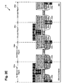
metal gates metal gate layer 224. Amask 226, shown inFigure 2E , is formed over thestructure 276 inFigure 2D and themetal gate layer 224 is etched to form themetal gates mask 226 covers at least a portion of themetal gate layer 224 over thedielectric segments metal gate layer 224 over thedielectric segments metal gate layer 224 over thedielectric segments metal gates - Referring now to
Figure 1 andFigure 2F , theprocess 100 includes forming a second metal gate layer (e.g., 228) and optionally a metal fill layer (e.g., 230) over the second gate layer in the first (e.g., 204a) and second (e.g., 204b) memory cell regions (180). InFigure 2F , astructure 280 corresponds to an implementation after forming ametal gate layer 228, and forming ametal fill layer 230 over themetal gate layer 228 in the substrate regions 204. - In some implementations, the
metal gate layer 228 includes metal for a gate of a high-k metal gate transistor, such as a P type high-k metal gate transistor. Suitable materials for the P type high-k metal gate transistor include, as specific examples, molybdenum (Mo), ruthenium (Ru), tantalum carbide nitride (TaCN), or other metal or metal stack. In other implementations, themetal gate layer 228 includes metal for a gate of a N type high-k metal gate transistor, or other types of transistors including non-high-k metal gate transistors. Themetal gate layer 228 can be formed by depositing a layer of metal over the dielectric segments 210 ofFigure 2E . The layer of metal can be deposited utilizing PVD, CVD, or another deposition technique. - In the implementation shown, the
metal fill layer 230 is formed over themetal gate layer 228. Themetal fill layer 230 can include metals of lower resistivity than the metal gate layers 224 and 228. Thus, themetal fill layer 230 can be used to provide low resistance contact to memory cell and logic transistors to be formed in the substrate regions 204. Examples of metals for themetal fill layer 230 include aluminum and copper. Themetal fill layer 230 can be formed by depositing a layer of metal over themetal gate layer 228. - Referring now to
Figure 1 andFigure 2G , theprocess 100 includes forming, from the second metal gate layer (e.g., 228), a second metal gate (e.g., 228b) of a second memory cell transistor (e.g., 234b), the second metal gate of a second work function (e.g., f2), the second memory cell transistor having a second threshold voltage (e.g., Vt2) (182). InFigure 2G , astructure 282 corresponds to an exemplary implementation after forming, from themetal gate layer 228, ametal gate 228b of amemory cell transistor 234b. Themetal gate 228b is of a work function f2 and thememory cell transistor 234b has a threshold voltage Vt2. - The present implementation includes optionally forming, from the
metal gate layer 228, ametal gate 228d of alogic transistor 234d. Themetal gate 228d is of the work function f2 and thelogic transistor 234d has a threshold voltage Vt4. Thememory cell transistor 234b is of a first conductivity type and thelogic transistor 234d is of a second conductivity type. Thus, themetal gates metal gate layer 228 while thelogic transistor 234d has the threshold voltage Vt4, which is different than the threshold voltage Vt2 of thememory cell transistor 234b. - The
metal gates metal gate layer 228 by performing a CMP or another type of planarization on thestructure 280 inFigure 2F . As an example, themetal gates memory cell transistors 234a and 234b and thelogic transistors Figure 2G . This may include formation of contacts for the transistors 234. - The memory cell transistor 234a includes the
metal gate 224a of the work function f1 and having the threshold voltage Vt1. The memory cell transistor 234a also optionally includes anoverlying gate segment 228a (including gate metal) formed from themetal gate layer 228 and situated over themetal gate 224a. As an example, theoverlying gate segment 228a can be approximately 10 nm to approximately 30 nm thick. Additionally, the memory cell transistor 234a optionally includes a metal fill 230a formed from themetal fill layer 230. - The
memory cell transistor 234b includes themetal gate 228b of the work function f2 and having the threshold voltage Vt2. Thememory cell transistor 234b also optionally includes ametal fill 230b formed from themetal fill layer 230. By utilizing themetal gates memory cell transistors 234a and 234b can be efficiently fabricated while having different threshold voltages Vt1 and Vt2. In the present implementation, themetal gate layer 224 includes metal for a gate of an N type high-k metal gate transistor and themetal gate layer 228 includes metal for a gate of a P type high-k metal gate transistor. This results in the threshold voltage Vt2 being greater than the threshold voltage Vt1. - The
logic transistor 234c includes themetal gate 224b of the work function f1 and having the threshold voltage Vt3. Thelogic transistor 234c also optionally includes an overlying gate segment 228c (including gate metal) formed from themetal gate layer 228 and situated over themetal gate 224b. As an example, the overlying gate segment 228c can be approximately 10 nm to approximately 30 nm thick. Additionally, thelogic transistor 234c optionally includes ametal fill 230c formed from themetal fill layer 230. - The
logic transistor 234d includes themetal gate 228d of the work function f2 and having the threshold voltage Vt4. thelogic transistor 234d also optionally includes ametal fill 230d formed from themetal fill layer 230. By utilizing themetal gates logic transistors metal gate layer 224 includes metal for a gate of an N type high-k metal gate transistor and themetal gate layer 228 includes metal for a gate of a P type high-k metal gate transistor. This results in the threshold voltage Vt4 being greater than the threshold voltage Vt3. - The
memory cell transistors 234a and 234b also respectively include thedielectric segments logic transistors dielectric segments - In the implementation shown, the
memory cell transistors 234a and 234b are of a first conductivity type and thelogic transistors memory cell transistors 234a and 234b are N type memory cell transistors respectively including achannel region 235a and achannel region 235b that are P type and the source/drain regions 220 that are N type. Thelogic transistors channel region 235c and achannel region 235d that are N type and the source/drain regions 220 that are P type. However, in some implementations, thememory cell transistors 234a and 234b are P type transistors and thelogic transistors Figures 2A ,2B ,2C ,2D ,2E ,2F , and2G demonstrate formation of four different transistors 234, any combination and number of the transistors 234 may be fabricated in various implementations. For example, in some implementations, only thememory cell transistors 234a and 234b and thelogic transistor 234d are fabricated. -
Figure 3 illustrates a top view of an exemplary IC including a ROM array. More particularly,Figure 3 illustrates anIC 300 including aROM array 336. TheROM array 336 includesmemory cell transistors 340, of whichmemory cell transistors IC 300 also includes logic transistors, of whichlogic transistors - The
IC 300 can be fabricated by utilizing theprocess 100, described above. In various implementations, the transistors 234 ofFigure 2G can correspond to any of thememory cell transistors 340 and thelogic transistors memory cell transistors 234a and 234b inFigure 2G correspond to any combination of thememory cell transistors 340. - As the
memory cell transistors 234a and 234b have different threshold voltages Vt1 and Vt2, thememory cell transistors 234a and 234b can correspond to different logical states in theROM array 336. More particularly, some of thememory cell transistors 340 are substantially similar to the memory cell transistor 234a so as to have the threshold voltage Vt1 corresponding to a first logical state. Others of thememory cell transistors 340 are substantially similar to thememory cell transistor 234b so as to have the threshold voltage Vt2 corresponding to a second logical state. - The
IC 300 is configured to sense the first and second logical states based on the threshold voltages Vt1 and Vt2. In some implementations, the threshold voltages Vt1 and Vt2 differ by at least approximately 100 mV. In some implementations, the threshold voltages Vt1 and Vt2 differ by approximately 200 mV to approximately 400 mV. - Thus, in accordance with some implementations, the
ROM array 336 can be programmed utilizing thememory cell transistors 234a and 234b including themetal gates ROM array 336 can have highly secure programming that is difficult to reverse engineer. More particularly, physical differences between thememory cell transistors 234a and 234b may not be readily apparent. Thus, it can be difficult to reverse engineer programming of theROM array 336 utilizing visual inspection or other non-invasive means. - Additionally, in some implementations, the
ROM array 336 can easily and inexpensively be fabricated with different programming by altering themask 226, which is a low grade mask. For example, the memory cell transistor 234a and thememory cell transistor 234b can have the source/drain regions 220 and thechannel regions Figure 2G can be made to have the threshold voltage Vt2 simply by changing themask 226 so that theoverlying gate segment 228a forms a metal gate of the memory cell transistor 234a. Similarly, thememory cell transistor 234b inFigure 2G can be made to have the threshold voltage Vt1 simply by changing themask 226 so that the overlying gate segment 228c forms a metal gate of the memory cell transistor 234a. - From the above description it is manifest that various techniques can be used for implementing the concepts described in the present application without departing from the scope of those concepts. Moreover, while the concepts have been described with specific reference to certain implementations, a person of ordinary skill in the art would recognize that changes can be made in form and detail without departing from the scope of those concepts. As such, the described implementations are to be considered in all respects as illustrative and not restrictive. It should also be understood that the present application is not limited to the particular implementations described above, but many rearrangements, modifications, and substitutions are possible without departing from the scope of the present disclosure.
Claims (15)
- An integrated circuit (IC) comprising:a first memory cell transistor of a read only memory (ROM) array, said first memory cell transistor comprising a first metal gate of a first work function and having a first threshold voltage;a second memory cell transistor of said ROM array, said second memory cell transistor comprising a second metal gate of a second work function and having a second threshold voltage.
- The IC of claim 1, wherein said first memory cell transistor and said second memory cell transistor are of a first conductivity type.
- The IC of claim 1, wherein said first memory cell transistor includes a first high-k gate dielectric and said second memory cell transistor includes a second high-k gate dielectric.
- The IC of claim 1 comprising an overlying gate segment situated over said first metal gate of said first memory cell transistor.
- The IC of claim 4, wherein said overlying gate segment is of said second work function.
- The IC of claim 1 comprising a first logic transistor, said first logic transistor having a third metal gate of said first work function and having a third threshold voltage.
- The IC of claim 6, wherein said first memory cell transistor is of a first conductivity type and said first logic transistor is of a second conductivity type.
- The IC of claim 1 comprising a second logic transistor, said second logic transistor having a fourth metal gate of said second work function and having a fourth threshold voltage.
- A method for fabricating an integrated circuit (IC), said method comprising:forming, from a first metal gate layer, a first metal gate of a first memory cell transistor of a read only memory (ROM) array, said first metal gate of a first work function and having a first threshold voltage;forming, from a second metal gate layer, a second metal gate of a second memory cell transistor of said ROM array, said second metal gate of a second work function and having a second threshold voltage.
- The method of claim 9, wherein said first memory cell transistor and said second memory cell transistor are of a first conductivity type.
- The method of claim 9, comprising forming a metal fill layer over said second metal gate layer.
- The method of claim 9, comprising forming, from said first metal gate layer, a third metal gate of a first logic transistor, said third metal gate of said first work function and having a third threshold voltage.
- The method of claim 12, wherein said first memory cell transistor is of a first conductivity type and said first logic transistor is of a second conductivity type.
- The method of claim 9, comprising forming, from said second metal gate layer, a fourth metal gate of a second logic transistor, said fourth metal gate of said second work function and having a fourth threshold voltage.
- A method for fabricating an integrated circuit (IC), said method comprising:forming, from a first metal gate layer, a first metal gate of a first N type memory cell transistor of a read only memory (ROM) array, said first metal gate of a first work function and having a first threshold voltage;forming, from a second metal gate layer, a second metal gate of a second N type memory cell transistor of said ROM array, said second metal gate of a second work function and having a second threshold voltage.
Applications Claiming Priority (1)
| Application Number | Priority Date | Filing Date | Title |
|---|---|---|---|
| US13/436,621 US9276004B2 (en) | 2012-03-30 | 2012-03-30 | ROM arrays having memory cell transistors programmed using metal gates |
Publications (2)
| Publication Number | Publication Date |
|---|---|
| EP2645419A2 true EP2645419A2 (en) | 2013-10-02 |
| EP2645419A3 EP2645419A3 (en) | 2017-03-29 |
Family
ID=46963362
Family Applications (1)
| Application Number | Title | Priority Date | Filing Date |
|---|---|---|---|
| EP12006387.0A Withdrawn EP2645419A3 (en) | 2012-03-30 | 2012-09-11 | ROM arrays having memory cell transistors programmed using metal gates |
Country Status (5)
| Country | Link |
|---|---|
| US (1) | US9276004B2 (en) |
| EP (1) | EP2645419A3 (en) |
| KR (1) | KR101393296B1 (en) |
| CN (1) | CN103367406B (en) |
| TW (1) | TWI546940B (en) |
Families Citing this family (1)
| Publication number | Priority date | Publication date | Assignee | Title |
|---|---|---|---|---|
| CN109687864A (en) * | 2017-10-19 | 2019-04-26 | 成都海存艾匹科技有限公司 | Programmable gate array containing programmable computing unit |
Citations (1)
| Publication number | Priority date | Publication date | Assignee | Title |
|---|---|---|---|---|
| US20110198699A1 (en) * | 2010-02-17 | 2011-08-18 | Taiwan Semiconductor Manufacturing Company, Ltd. | Integrated semiconductor structure for sram and fabrication methods thereof |
Family Cites Families (9)
| Publication number | Priority date | Publication date | Assignee | Title |
|---|---|---|---|---|
| TW344137B (en) | 1996-12-09 | 1998-11-01 | United Microelectronics Corp | Multi-stage read-only memory structure and process for producing the same |
| US6417548B1 (en) * | 1999-07-19 | 2002-07-09 | United Microelectronics Corp. | Variable work function transistor high density mask ROM |
| US7019351B2 (en) * | 2003-03-12 | 2006-03-28 | Micron Technology, Inc. | Transistor devices, and methods of forming transistor devices and circuit devices |
| JP2007258224A (en) * | 2006-03-20 | 2007-10-04 | Renesas Technology Corp | Semiconductor integrated circuit device and manufacturing method thereof |
| US8217435B2 (en) * | 2006-12-22 | 2012-07-10 | Intel Corporation | Floating body memory cell having gates favoring different conductivity type regions |
| DE102007046849B4 (en) * | 2007-09-29 | 2014-11-06 | Advanced Micro Devices, Inc. | Method of making large-gate-gate structures after transistor fabrication |
| JP5464853B2 (en) | 2008-12-29 | 2014-04-09 | ルネサスエレクトロニクス株式会社 | Manufacturing method of semiconductor device |
| US8119473B2 (en) | 2009-12-31 | 2012-02-21 | Taiwan Semiconductor Manufacturing Company, Ltd. | High temperature anneal for aluminum surface protection |
| US20130049119A1 (en) * | 2011-08-29 | 2013-02-28 | Shanghai Huali Microelectronics Corporation | Multi-working voltages cmos device with single gate oxide layer thickness and manufacturing method thereof |
-
2012
- 2012-03-30 US US13/436,621 patent/US9276004B2/en active Active
- 2012-09-11 EP EP12006387.0A patent/EP2645419A3/en not_active Withdrawn
- 2012-09-27 CN CN201210366066.3A patent/CN103367406B/en not_active Expired - Fee Related
- 2012-09-27 KR KR1020120107915A patent/KR101393296B1/en not_active Expired - Fee Related
- 2012-10-17 TW TW101138245A patent/TWI546940B/en not_active IP Right Cessation
Patent Citations (1)
| Publication number | Priority date | Publication date | Assignee | Title |
|---|---|---|---|---|
| US20110198699A1 (en) * | 2010-02-17 | 2011-08-18 | Taiwan Semiconductor Manufacturing Company, Ltd. | Integrated semiconductor structure for sram and fabrication methods thereof |
Also Published As
| Publication number | Publication date |
|---|---|
| TW201340296A (en) | 2013-10-01 |
| CN103367406A (en) | 2013-10-23 |
| EP2645419A3 (en) | 2017-03-29 |
| TWI546940B (en) | 2016-08-21 |
| KR20130111166A (en) | 2013-10-10 |
| US20130256804A1 (en) | 2013-10-03 |
| CN103367406B (en) | 2017-05-31 |
| US9276004B2 (en) | 2016-03-01 |
| KR101393296B1 (en) | 2014-05-09 |
Similar Documents
| Publication | Publication Date | Title |
|---|---|---|
| CN100487911C (en) | Bimetallic grid transistor for CMOS process and manufacturing method thereof | |
| US7871915B2 (en) | Method for forming metal gates in a gate last process | |
| US20180337113A1 (en) | Semiconductor Device with Multi Level Interconnects and Method of Forming the Same | |
| US20110298045A1 (en) | Self-aligned contact for trench mosfet | |
| US20150236106A1 (en) | Method for creating self-aligned transistor contacts | |
| US20070215917A1 (en) | Semiconductor integrated circuit device and a method of manufacturing the same | |
| US11569369B2 (en) | Method for manufacturing a semiconductor device | |
| CN110277369B (en) | A fuse structure of dynamic random access memory element | |
| US9129856B2 (en) | Method for efficiently fabricating memory cells with logic FETs and related structure | |
| US8816449B2 (en) | Self-aligned MOS structure with local interconnects and self-aligned source/drain polysilicon contacts | |
| KR100561552B1 (en) | Method of Fabricating Semiconductor Device | |
| CN103426825B (en) | Semiconductor manufacturing process and semiconductor structure | |
| US11088254B2 (en) | Semiconductor device and method of manufacturing the same | |
| KR101393296B1 (en) | Rom arrays having memory cell transistors programmed using metal gates | |
| HK1186838A (en) | An integrated circuit including a first memory cell transistor of a read only memory array and fabricating method thereof | |
| US7416968B2 (en) | Methods of forming field effect transistors having metal silicide gate electrodes | |
| US12482706B2 (en) | Semiconductor structure that includes self-aligned contact plugs and methods for manufacturing the same | |
| EP1146556A1 (en) | A process for fabricating an integrated ciruit that has embedded dram and logic devices | |
| CN111081548A (en) | Fully silicided gated device and method of forming the same | |
| CN122054672A (en) | Manufacturing method of integrated structure of metal gate MOS transistor | |
| KR100958630B1 (en) | Method of manufacturing semiconductor device | |
| KR20070002664A (en) | Dual gate manufacturing method of semiconductor device | |
| US8748252B1 (en) | Replacement metal gate transistors using bi-layer hardmask | |
| CN101556921A (en) | Semiconductor device and method for manufacturing the same | |
| KR20070069634A (en) | Gate electrode formation method of semiconductor device |
Legal Events
| Date | Code | Title | Description |
|---|---|---|---|
| PUAI | Public reference made under article 153(3) epc to a published international application that has entered the european phase |
Free format text: ORIGINAL CODE: 0009012 |
|
| 17P | Request for examination filed |
Effective date: 20120911 |
|
| AK | Designated contracting states |
Kind code of ref document: A2 Designated state(s): AL AT BE BG CH CY CZ DE DK EE ES FI FR GB GR HR HU IE IS IT LI LT LU LV MC MK MT NL NO PL PT RO RS SE SI SK SM TR |
|
| AX | Request for extension of the european patent |
Extension state: BA ME |
|
| RIN1 | Information on inventor provided before grant (corrected) |
Inventor name: XIA, WEI |
|
| PUAL | Search report despatched |
Free format text: ORIGINAL CODE: 0009013 |
|
| STAA | Information on the status of an ep patent application or granted ep patent |
Free format text: STATUS: EXAMINATION IS IN PROGRESS |
|
| AK | Designated contracting states |
Kind code of ref document: A3 Designated state(s): AL AT BE BG CH CY CZ DE DK EE ES FI FR GB GR HR HU IE IS IT LI LT LU LV MC MK MT NL NO PL PT RO RS SE SI SK SM TR |
|
| AX | Request for extension of the european patent |
Extension state: BA ME |
|
| RIC1 | Information provided on ipc code assigned before grant |
Ipc: H01L 29/49 20060101ALI20170220BHEP Ipc: H01L 21/8234 20060101ALI20170220BHEP Ipc: H01L 21/8238 20060101ALI20170220BHEP Ipc: H01L 21/28 20060101ALI20170220BHEP Ipc: H01L 27/112 20060101AFI20170220BHEP |
|
| 17Q | First examination report despatched |
Effective date: 20170320 |
|
| RAP1 | Party data changed (applicant data changed or rights of an application transferred) |
Owner name: AVAGO TECHNOLOGIES GENERAL IP (SINGAPORE) PTE. LTD |
|
| RBV | Designated contracting states (corrected) |
Designated state(s): AL AT BE BG CH CY CZ DE DK EE ES FI FR GB GR HR HU IE IS IT LI LT LU LV MC MK MT NL NO PL PT RO RS SE SI SK SM TR |
|
| RAP1 | Party data changed (applicant data changed or rights of an application transferred) |
Owner name: AVAGO TECHNOLOGIES INTERNATIONAL SALES PTE. LIMITE |
|
| STAA | Information on the status of an ep patent application or granted ep patent |
Free format text: STATUS: THE APPLICATION IS DEEMED TO BE WITHDRAWN |
|
| 18D | Application deemed to be withdrawn |
Effective date: 20211005 |