EP2642654A1 - Switching rectifier circuit and battery charger using same - Google Patents
Switching rectifier circuit and battery charger using same Download PDFInfo
- Publication number
- EP2642654A1 EP2642654A1 EP11841625.4A EP11841625A EP2642654A1 EP 2642654 A1 EP2642654 A1 EP 2642654A1 EP 11841625 A EP11841625 A EP 11841625A EP 2642654 A1 EP2642654 A1 EP 2642654A1
- Authority
- EP
- European Patent Office
- Prior art keywords
- voltage
- turn
- threshold voltage
- switch
- detection signal
- Prior art date
- Legal status (The legal status is an assumption and is not a legal conclusion. Google has not performed a legal analysis and makes no representation as to the accuracy of the status listed.)
- Granted
Links
Images







Classifications
-
- H—ELECTRICITY
- H02—GENERATION; CONVERSION OR DISTRIBUTION OF ELECTRIC POWER
- H02M—APPARATUS FOR CONVERSION BETWEEN AC AND AC, BETWEEN AC AND DC, OR BETWEEN DC AND DC, AND FOR USE WITH MAINS OR SIMILAR POWER SUPPLY SYSTEMS; CONVERSION OF DC OR AC INPUT POWER INTO SURGE OUTPUT POWER; CONTROL OR REGULATION THEREOF
- H02M7/00—Conversion of AC power input into DC power output; Conversion of DC power input into AC power output
- H02M7/02—Conversion of AC power input into DC power output without possibility of reversal
- H02M7/04—Conversion of AC power input into DC power output without possibility of reversal by static converters
- H02M7/12—Conversion of AC power input into DC power output without possibility of reversal by static converters using discharge tubes with control electrode or semiconductor devices with control electrode
- H02M7/21—Conversion of AC power input into DC power output without possibility of reversal by static converters using discharge tubes with control electrode or semiconductor devices with control electrode using devices of a triode or transistor type requiring continuous application of a control signal
- H02M7/217—Conversion of AC power input into DC power output without possibility of reversal by static converters using discharge tubes with control electrode or semiconductor devices with control electrode using devices of a triode or transistor type requiring continuous application of a control signal using semiconductor devices only
- H02M7/219—Conversion of AC power input into DC power output without possibility of reversal by static converters using discharge tubes with control electrode or semiconductor devices with control electrode using devices of a triode or transistor type requiring continuous application of a control signal using semiconductor devices only in a bridge configuration
-
- H—ELECTRICITY
- H02—GENERATION; CONVERSION OR DISTRIBUTION OF ELECTRIC POWER
- H02J—ELECTRIC POWER NETWORKS; CIRCUIT ARRANGEMENTS OR SYSTEMS FOR SUPPLYING OR DISTRIBUTING ELECTRIC POWER; SYSTEMS FOR STORING ELECTRIC ENERGY
- H02J7/00—Circuit arrangements for charging or discharging batteries or for supplying loads from batteries
- H02J7/02—Circuit arrangements for charging or discharging batteries or for supplying loads from batteries for charging batteries from AC mains by converters
-
- H—ELECTRICITY
- H02—GENERATION; CONVERSION OR DISTRIBUTION OF ELECTRIC POWER
- H02J—ELECTRIC POWER NETWORKS; CIRCUIT ARRANGEMENTS OR SYSTEMS FOR SUPPLYING OR DISTRIBUTING ELECTRIC POWER; SYSTEMS FOR STORING ELECTRIC ENERGY
- H02J2207/00—Details of circuit arrangements for charging or discharging batteries or supplying loads from batteries
- H02J2207/20—Charging or discharging characterised by the power electronics converter
-
- H—ELECTRICITY
- H02—GENERATION; CONVERSION OR DISTRIBUTION OF ELECTRIC POWER
- H02M—APPARATUS FOR CONVERSION BETWEEN AC AND AC, BETWEEN AC AND DC, OR BETWEEN DC AND DC, AND FOR USE WITH MAINS OR SIMILAR POWER SUPPLY SYSTEMS; CONVERSION OF DC OR AC INPUT POWER INTO SURGE OUTPUT POWER; CONTROL OR REGULATION THEREOF
- H02M7/00—Conversion of AC power input into DC power output; Conversion of DC power input into AC power output
- H02M7/02—Conversion of AC power input into DC power output without possibility of reversal
- H02M7/04—Conversion of AC power input into DC power output without possibility of reversal by static converters
- H02M7/12—Conversion of AC power input into DC power output without possibility of reversal by static converters using discharge tubes with control electrode or semiconductor devices with control electrode
- H02M7/21—Conversion of AC power input into DC power output without possibility of reversal by static converters using discharge tubes with control electrode or semiconductor devices with control electrode using devices of a triode or transistor type requiring continuous application of a control signal
- H02M7/217—Conversion of AC power input into DC power output without possibility of reversal by static converters using discharge tubes with control electrode or semiconductor devices with control electrode using devices of a triode or transistor type requiring continuous application of a control signal using semiconductor devices only
- H02M7/219—Conversion of AC power input into DC power output without possibility of reversal by static converters using discharge tubes with control electrode or semiconductor devices with control electrode using devices of a triode or transistor type requiring continuous application of a control signal using semiconductor devices only in a bridge configuration
- H02M7/2195—Conversion of AC power input into DC power output without possibility of reversal by static converters using discharge tubes with control electrode or semiconductor devices with control electrode using devices of a triode or transistor type requiring continuous application of a control signal using semiconductor devices only in a bridge configuration the switches being synchronously commutated at the same frequency of the AC input voltage
Definitions
- the present invention relates to switching rectifier circuits, and to battery chargers using them.
- a full-wave rectification circuit 100 using a diode bridge as shown in Fig. 19 is commonly used.
- the diodes 101 to 104 constituting the diode bridge have a high forward voltage drop, which causes energy loss (power loss or heat generation in the diodes 101 to 104) during the periods in which current I passes through the diodes 101 to 104 (see the hatched areas in Fig. 20 ).
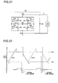
- a switching rectifier circuit 200 in which, as shown in Fig. 21 , diodes 101 to 104 as mentioned above are replaced with transistors 201 to 204, which are turned on and off with proper timing so as to convert an AC voltage VAC into a DC voltage VDC.
- the timing with which the turning on and off of the transistor 201 is controlled is determined based on the comparison output from a comparator 206 (an output resulting from comparison between the DC voltage VDC and a first AC voltage VAC1); the timing with which the turning on and off of the transistor 202 is controlled is determined based on the comparison output from a comparator 207 (an output resulting from comparison between the DC voltage VDC and a second AC voltage VAC2).
- the timing with which the turning on and off of the transistor 203 is controlled is determined based on the comparison output from a comparator 208 (an output resulting from comparison between the reference voltage VSS and the first AC voltage VAC1); the timing with which the turning on and off of the transistor 204 is controlled is determined based on the comparison output from a comparator 209 (an output resulting from comparison between the reference voltage VSS and the second AC voltage VAC1).
- Patent Documents 1 and 2 listed below.
- Patent Document 1 Japanese Patent Application Publication No. H9-131064
- Patent Document 2 United States Patent Application Publication No. 2009/0016090
- the conventional switching rectifier circuit 200 configured as described above, it is difficult to accurately control the timing with which the transistors 201 to 204 are turned on and off. Consequently, the transistors 201 and 204 (or 202 and 203) cannot be turned off reliably before the first AC voltage VAC1 (or the second AC voltage VAC2) decreases under the DC voltage VDC, and this may cause a reverse-flow current from an output capacitor 205, leading to diminished power conversion efficiency (see Fig. 22 ).
- the present invention aims to provide a switching rectifier circuit that contributes to higher power conversion efficiency, and to provide a battery charger employing such a switching rectifier circuit.
- a switching rectification circuit includes: a first switch connected between a terminal to which a first AC voltage is applied and a terminal to which a DC voltage is applied; a second switch connected between a terminal to which a second AC voltage is applied and the terminal to which the DC voltage is applied; a third switch connected between the terminal to which the first AC voltage is applied and a terminal to which a reference voltage is applied; a fourth switch connected between the terminal to which the second AC voltage is applied and the terminal to which the reference voltage is applied; a first comparison circuit adapted to generate from the first AC voltage and the DC voltage a first on detection signal and a first off detection signal individually; a second comparison circuit adapted to generate from the second AC voltage and the DC voltage a second on detection signal and a second off detection signal individually; and a timing generator adapted to control the turning on and off of the first to fourth switches based on at least the outputs of the first and second comparison circuits (a first configuration).
- the first comparison circuit includes: a first hysteresis comparator adapted to turn the first on detection signal to high level or low level when the first AC voltage increases over a first threshold voltage higher than the DC voltage and turn the first on detection signal to low level or high level when the first AC voltage decreases under a third threshold voltage lower than the DC voltage; and a first comparator adapted to turn the first off detection signal to high level or low level when the first AC voltage increases over a second threshold voltage higher than the DC voltage but lower than the first threshold voltage and turn the first off detection signal to low level or high level when the first AC voltage decreases under the second threshold voltage.
- the second comparison circuit includes: a second hysteresis comparator adapted to turn the second on detection signal to high level or low level when the second AC voltage increases over the first threshold voltage and turn the second on detection signal to low level or high level when the second AC voltage decreases under the third threshold voltage; and a second comparator adapted to turn the second off detection signal to high level or low level when the second AC voltage increases over the second threshold and turn the second off detection signal to low level or high level when the second AC voltage decreases under the second threshold voltage (a second configuration).
- a third comparison circuit adapted to generate from the first AC voltage and the reference voltage a third detection signal
- a fourth comparison circuit adapted to generate from the second AC voltage and the reference voltage a fourth detection signal.
- the timing controller is adapted to control the turning on and off of the first to fourth switches based on at least the outputs of the first to fourth comparison circuits (a third configuration).
- the third comparison circuit includes a third hysteresis comparator adapted to turn the third detection signal to high level or low level when the first AC voltage decreases under a fourth threshold voltage lower than the reference voltage and turn the third detection signal to low level or high level when the first AC voltage increases over a fifth threshold voltage higher than the reference voltage
- the fourth comparison circuit includes a fourth hysteresis comparator adapted to turn the fourth detection signal to high level or low level when the second AC voltage decreases under the fourth threshold voltage and turn the fourth detection signal to low level or high level when the second AC voltage increases over the fifth threshold voltage (a fourth configuration).
- a time constant circuit adapted to generate an enable signal which remains at high level or low level after the first or second AC voltage increases over the first threshold voltage until a predetermined time elapses.
- the timing controller is adapted to control the turning on and off of the first to fourth switches based on at least the outputs of the first to fourth comparison circuits and of the time constant circuit (a fifth configuration).
- the predetermined time is controlled to vary so as to be the shorter the higher the voltage level of the DC voltage is (a sixth configuration).
- the timing generator is adapted to generate the first on and off control signals so as to turn on the first switch when the first AC voltage increases over the first threshold voltage and turn off the first switch when the first AC voltage decreases under the second threshold voltage, generate the second on and off control signals so as to turn on the second switch when the second AC voltage increases over the first threshold voltage and turn off the second switch when the second AC voltage decreases under the second threshold voltage, generate the third on and off control signals so as to turn on the third switch a first wait time after the first AC voltage decreases under the fourth threshold voltage and turn off the third switch when the second AC voltage decreases under the fourth threshold voltage, and generate the fourth on and off control signals so as to turn on the fourth switch a second wait time after the second AC voltage decreases under the fourth threshold voltage and turn off the fourth switch when the first AC voltage decreases under the fourth threshold voltage (a seventh configuration).
- the timing generator is adapted to generate the first on and off control signals so as to turn on the first switch when the first AC voltage increases over the first threshold voltage and turn off the first switch when the first AC voltage decreases under the second threshold voltage or a predetermined time after the first AC voltage has increased over the first threshold voltage, generate the second on and off control signals so as to turn on the second switch when the second AC voltage increases over the first threshold voltage and turn off the second switch when the second AC voltage decreases under the second threshold voltage or a predetermined time after the second AC voltage has increased over the first threshold voltage, generate the third on and off control signals so as to turn on the third switch a first wait time after the first AC voltage decreases under the fourth threshold voltage and turn off the third switch when the second AC voltage decreases under the fourth threshold voltage, and generate the fourth on and off control signals so as to turn on the fourth switch a second wait time after the second AC voltage decreases under the fourth threshold voltage and turn off the fourth switch when the first AC voltage decreases under the fourth threshold voltage
- the timing generator is adapted to generate the first on and off control signals so as to turn on the first switch when the first AC voltage increases over the first threshold voltage and turn off the first switch when the first AC voltage decreases under the second threshold voltage, generate the second on and off control signals so as to turn on the second switch when the second AC voltage increases over the first threshold voltage and turn off the second switch when the second AC voltage decreases under the second threshold voltage, generate the third on and off control signals so as to turn on the third switch when the first AC voltage decreases under the fourth threshold voltage and turn off the third switch when the second AC voltage decreases under the second threshold voltage, and generate the fourth on and off control signals so as to turn on the fourth switch when the second AC voltage decreases under the fourth threshold voltage and turn off the fourth switch when the first AC voltage decreases under the second threshold voltage (a ninth configuration).
- the timing generator is adapted to generate the first on and off control signals so as to turn on the first switch when the first AC voltage increases over the first threshold voltage and turn off the first switch when the first AC voltage decreases under the second threshold voltage, generate the second on and off control signals so as to turn on the second switch when the second AC voltage increases over the first threshold voltage and turn off the second switch when the second AC voltage decreases under the second threshold voltage, generate the third on and off control signals so as to turn on the third switch when the second AC voltage increases over the first threshold voltage and turn off the third switch when the second AC voltage decreases under the fourth threshold voltage, and generate the fourth on and off control signals so as to turn on the fourth switch when the first AC voltage increases over the first threshold voltage and turn off the fourth switch when the first AC voltage decreases under the fourth threshold voltage (a tenth configuration).
- the timing generator is adapted to generate the first and fourth on and off control signals so as to turn on both the first and fourth switches when the first AC voltage increases over the first threshold voltage and turn off both the first and fourth switches when the first AC voltage decreases under the second threshold voltage, and generate the second and third on and off control signals so as to turn on both the second and third switches when the second AC voltage increases over the first threshold voltage and turn off both the second and third switches when the second AC voltage decreases under the second threshold voltage (an eleventh configuration).
- the timing generator is adapted to ignore a drop in the first and second AC voltages under the second threshold voltage when turning on the first and second switches respectively (a twelfth configuration).
- switching rectification circuit includes: a first switch connected between a terminal to which a first AC voltage is applied and a terminal to which a DC voltage is applied; a second switch connected between a terminal to which a second AC voltage is applied and the terminal to which the DC voltage is applied; a third switch connected between the terminal to which the first AC voltage is applied and a terminal to which a reference voltage is applied; a fourth switch connected between the terminal to which the second AC voltage is applied and the terminal to which the reference voltage is applied; a first comparison circuit adapted to generate from the first AC voltage and the DC voltage a first detection signal; a second comparison circuit adapted to generate from the second AC voltage and the DC voltage a second detection signal; a third comparison circuit adapted to generate from the first AC voltage and the reference voltage a third detection signal; a fourth comparison circuit adapted to generate from the second AC voltage and the reference voltage a fourth detection signal; and a timing generator adapted to control the turning on and off of the first to fourth switches based on at least the outputs
- the first comparison circuit includes a first hysteresis comparator adapted to turn the first detection signal to high level or low level when the first AC voltage increases over a first threshold voltage higher than the DC voltage and turn the first detection signal to low level or high level when the first AC voltage decreases under a second threshold voltage higher than the DC voltage but lower than the first threshold voltage
- the second comparison circuit includes a second hysteresis comparator adapted to turn the second detection signal to high level or low level when the second AC voltage increases over the first threshold voltage and turn the second detection signal to low level or high level when the second AC voltage decreases under the second threshold voltage
- the third comparison circuit includes a third hysteresis comparator adapted to turn the third detection signal to high level or low level when the first AC voltage decreases under a third threshold voltage lower than the reference voltage and turn the third detection signal to low level or high level when the first AC voltage increases over a fourth threshold voltage higher than the reference voltage
- the fourth comparison circuit includes
- the first comparison circuit includes a first hysteresis comparator adapted to turn the first detection signal to high level or low level when the first AC voltage increases over a first threshold voltage higher than the DC voltage and turn the first detection signal to low level or high level when the first AC voltage decreases under a second threshold voltage lower than the DC voltage
- the second comparison circuit includes a second hysteresis comparator adapted to turn the second detection signal to high level or low level when the second AC voltage increases over the first threshold voltage and turn the second detection signal to low level or high level when the second AC voltage decreases under the second threshold voltage
- the third comparison circuit includes a third hysteresis comparator adapted to turn the third detection signal to high level or low level when the first AC voltage decreases under a third threshold voltage lower than the reference voltage and turn the third detection signal to low level or high level when the first AC voltage increases over a fourth threshold voltage higher than the reference voltage
- the fourth comparison circuit includes a fourth hyster
- the timing controller is adapted to control the turning on and off of the first to fourth switches based on at least the outputs of the first to fourth comparison circuits and of the time constant circuit (a sixteenth configuration).
- the predetermined time is controlled to vary so as to be the shorter the higher the voltage level of the DC voltage is (a seventeenth configuration).
- the timing generator is adapted to generate the first on and off control signals so as to turn on the first switch when the first AC voltage increases over the first threshold voltage and turn off the first switch when the first AC voltage decreases under the second threshold voltage, generate the second on and off control signals so as to turn on the second switch when the second AC voltage increases over the first threshold voltage and turn off the second switch when the second AC voltage decreases under the second threshold voltage, generate the third on and off control signals so as to turn on the third switch a first wait time after the first AC voltage decreases under the third threshold voltage and turn off the third switch when the second AC voltage decreases under the third threshold voltage, and generate the fourth on and off control signals so as to turn on the fourth switch a second wait time after the second AC voltage decreases under the third threshold voltage and turn off the fourth switch when the first AC voltage decreases under the third threshold voltage (an eighteenth configuration).
- the timing generator is adapted to generate the first on and off control signals so as to turn on the first switch when the first AC voltage increases over the first threshold voltage and turn off the first switch when the first AC voltage decreases under the second threshold voltage or a predetermined time after the first AC voltage has increased over the first threshold voltage, generate the second on and off control signals so as to turn on the second switch when the second AC voltage increases over the first threshold voltage and turn off the second switch when the second AC voltage decreases under the second threshold voltage or a predetermined time after the second AC voltage has increased over the first threshold voltage, generate the third on and off control signals so as to turn on the third switch a first wait time after the first AC voltage decreases under the third threshold voltage and turn off the third switch when the second AC voltage decreases under the third threshold voltage, and generate the fourth on and off control signals so as to turn on the fourth switch a second wait time after the second AC voltage decreases under the third threshold voltage and turn off the fourth switch when the first AC voltage decreases under
- the timing generator is adapted to ignore a drop in the first and second AC voltages under the second threshold voltage when turning on the first and second switches respectively (a twentieth configuration).
- the first to fourth switches are all field-effect transistors (a twenty-first configuration).
- the timing controller is adapted to keep the first to fourth switches all off until the DC voltage reaches a predetermined level and rectify the AC voltages into the DC voltage through rectification operation using body diodes of the first to fourth switches respectively (a twenty-second configuration).
- a battery charger includes the switching rectifier circuit according to any one of the first to twenty-second configurations described above, and the controls the charging of a battery cell by using the DC voltage (a twenty-third configuration).
- a transformer coupling between a commercial AC power source and the switching rectifier circuit on a non-contact basis (a twenty-fourth configuration).
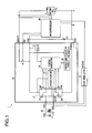
- Fig. 1 is a block diagram showing an exemplary configuration of a battery charger according to the invention.
- the battery charger 1 of this exemplary configuration includes a switching rectifier IC 10, a transformer 20, a microprocessor 30, and a load modulator 40, and controls the charging of a battery cell 3 by use of a DC (direct-current) voltage VDC obtained by rectifying on a full-wave basis an AC (alternating-current) voltage VAC from a commercial AC power source 2.
- the switching rectifier IC 10 has integrated into it an H bridge 11, a discriminator 12, a timing generator 13, an undervoltage detector 14 (UVLO, undervoltage lock-out), a protection circuit 15, an overvoltage detector 16 (OVP, overvoltage protection), an abnormal temperature detector 17 (TSD, thermal shutdown), and a switch 18.
- the switching rectifier IC 10 Connected to the switching rectifier IC 10 externally to it are the transformer 20, the microprocessor 30, the load modulator 40, the battery cell 3, and discrete components such as an output capacitor C1.
- the configuration of the switching rectifier IC 10 will be described in detail later.
- the transformer 20 serves as a means of connecting between the commercial AC power source 2 and the switching rectifier IC 1 on a non-contact basis, and has a primary coil L1 and a secondary coil L2.
- the microprocessor 30 receives a DC voltage VDC from the switching rectifier IC 10, and operates to monitor the battery voltage VBATT, generate a switch signal SW, generate a modulation input signal MODIN, and otherwise.
- the load modulator 40 transfers the modulation input signal MODIN fed from the microprocessor 30 to the primary side via the transformer 20.
- the H bridge 11 is composed of P-channel MOS field-effect transistors M1 and M2 and N-channel MOS field-effect transistors M3 and M4 connected in an H bridge configuration.
- the source and backgate of the transistor M1 are both connected to a terminal to which the DC voltage VDC is applied.
- the drain of the transistor M1 is connected to a terminal to which a first AC voltage VAC1 (the AC voltage appearing at a first end of the secondary coil L2) is applied.
- the gate of the transistor M1 is connected to the timing generator 13 (specifically, to a terminal to which a first gate signal G1 is output).
- the transistor M1 corresponds to a first switch connected between the terminals to which the first AC voltage VAC1 and the DC voltage VDC, respectively, are applied.
- the source and backgate of the transistor M2 are both connected to the terminal to which the DC voltage VDC is applied.
- the drain of the transistor M2 is connected to a terminal to which a second AC voltage VAC2 (the AC voltage appearing at a second end of the secondary coil L2) is applied.
- the gate of the transistor M2 is connected to the timing generator 13 (specifically, to a terminal to which a second gate signal G2 is output).
- the transistor M2 corresponds to a second switch connected between the terminals to which the second AC voltage VAC2 and the DC voltage VDC, respectively, are applied.
- the source and backgate of the transistor M3 are both connected to a terminal to which a reference voltage VSS (in Fig. 1 , a ground voltage PGND) is applied.
- the drain of the transistor M3 is connected to the terminal to which the first AC voltage VAC1 is applied.
- the gate of the transistor M3 is connected to the timing generator 13 (specifically, to a terminal to which a third gate signal G3 is output).
- the transistor M3 corresponds to a third switch connected between the terminals to which the first AC voltage VAC1 and the reference voltage VSS, respectively, are applied.
- the source and backgate of the transistor M4 are both connected to the terminal to which the reference voltage VSS is applied.
- the drain of the transistor M4 is connected to the terminal to which the second AC voltage VAC2 is applied.
- the gate of the transistor M4 is connected to the timing generator 13 (specifically, to a terminal to which a fourth gate signal G4 is output).
- the transistor M4 corresponds to a fourth switch connected between the terminals to which the second AC voltage VAC2 and the reference voltage VSS, respectively, are applied.
- transistors M1 to M4 power-path MOS FETs with a low on-state resistance.
- the discriminator 12 compares each of the first and second AC voltages VAC1 and VAC2 with each of the DC voltage VDC and the reference voltage VSS, generates detection signals reflecting the results of the comparisons, and feeds them to the timing generator 13.
- the specific circuit configuration and operation of the discriminator 12 will be described in detail later.
- the timing generator 13 turns on and off the transistors M1 to M4 based on the detection signals fed from the discriminator 12.
- the timing generator 13 also has the function of stopping the rectification operation by turning the transistors M1 to M4 all off, or by turning the transistors M3 and M4 both on and thereby short-circuiting both ends of the primary coil L1, based on an undervoltage protection signal fed from the undervoltage detector 14 and a fault protection signal fed from the protection circuit 15.
- the specific operation of the timing generator 13 will be described in detail later.
- the undervoltage detector 14 generates an undervoltage protection signal which indicates whether or not the DC voltage VDC is equal to or higher than a predetermined level, and feeds it to the timing generator 13. Based on the undervoltage protection signal, the timing generator 13 keeps the transistors M1 to M4 all off until the DC voltage VDC reaches the predetermined level. Specifically, until the DC voltage VDC reaches the predetermined level, the switching rectifier IC 10 rectifies the AC voltage VAC into the DC voltage VDC through rectification operation using the body diodes D1 to D4 (see Figs. 2A, 2B , 3 , etc.) parasitic to the transistors M1 to M4 respectively.
- the protection circuit 15 Based on an overvoltage detection signal fed from the overvoltage detector 16 and an abnormal temperature detection signal fed from the abnormal temperature detector 17, the protection circuit 15 generates a fault protection signal which indicates whether or not there is some fault in the switching rectifier IC 10, and feeds it to the timing generator 13.
- the timing generator 13 recognizes that there is some fault in the switching rectifier IC 10 based on the fault protection signal, it forcibly stops the transistors M1 to M4.
- the overvoltage detector 16 generates an overvoltage detection signal which indicates whether or not the DC voltage VDC is equal to or higher than a predetermined level, and feeds it to the protection circuit 15.
- the abnormal temperature detector 17 generates an abnormal temperature detection signal which indicates whether or not the internal temperature of the switching rectifier IC 10 equal to or higher than a predetermined level, and feeds it to the protection circuit 15.
- a first terminal of the switch 18 is connected to a terminal to which the battery voltage VBATT is applied.
- a second terminal of the switch 18 is connected to the terminal to which the DC voltage VDC is applied.
- the control terminal of the switch 18 is connected to a terminal to which the switch signal SW is fed.
- a switching rectifier circuit that rectifies the AC voltage VAC on a full-wave basis to produce the DC voltage VDC is constituted by, of the components mentioned above, the H bridge 11, the discriminator 12, the timing generator 13, and the output capacitor C1 in particular.
- Figs. 2A and 2B are circuit diagrams illustrating switching rectification operation.
- current I passes through the path shown in Fig. 2A , and the output capacitor C1 is charged.
- current I passes through the path shown in Fig. 2B , and the output capacitor C1 is charged.
- the AC voltage VAC is rectified on a full-wave basis into the DC voltage VDC.
- the AC voltage VAC is rectified into the DC voltage VDC through rectification operation using the body diodes D1 to D4.
- Fig. 3 is a circuit diagram of a switching rectifier circuit according to a first embodiment of the invention.
- the switching rectifier circuit according to the first embodiment has, as the discriminator 12, comparison circuits 121 to 124.
- the comparison circuit 121 receives the first AC voltage VAC and the DC voltage VDC, and generates a first on detection signal DET1a and a first off detection signal DEX1b individually.
- the comparison circuit 122 receives the second AC voltage VAC and the DC voltage VDC, and generates a second on detection signal DET2a and a second off detection signal DET2b individually.
- the comparison circuit 123 receives the first AC voltage VAC and the reference voltage VSS, and generates a third detection signal DET3.
- the comparison circuit 124 receives the second AC voltage VAC2 and the reference voltage VSS, and generates a fourth detection signal DET4.
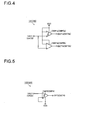
- Fig. 4 is a circuit diagram showing one exemplary configuration of the comparison circuits 121 and 122.
- the comparison circuit 121 includes a hysteresis comparator CMP1a and a comparator CMP1b
- the comparison circuit 122 includes a hysteresis comparator CMP2a and a comparator CMP2b.
- the non-inverting input terminal (+) of the hysteresis comparator CMP1a is connected to the terminal to which the first AC voltage VAC1 is applied.
- the inverting input terminal (-) of the hysteresis comparator CMP1a is connected to the terminal to which the DC voltage VDC is applied.
- the hysteresis comparator CMP1a is configured to compare the first AC voltage VAC1 with a first threshold voltage (VDC + X1), which is higher than the DC voltage VDC by a first offset voltage X1, and with a third threshold voltage (VDC - X3), which is lower than the DC voltage VDC by a third offset voltage X3, in order to switch the logic level of the first on detection signal DET1a.
- the hysteresis comparator CMP1a turns the first on detection signal DET1a to high level; when the first AC voltage VAC1 decreases under the third threshold voltage (VDC - X3), the hysteresis comparator CMP1a turns the first on detection signal DET1a to low level.
- the non-inverting input terminal (+) of the comparator CMP1b is connected to the terminal to which the first AC voltage VAC1 is applied.
- the inverting input terminal (-) of the comparator CMP1b is connected to the terminal to which the DC voltage VDC is applied.
- the comparator CMP1b is configured to compare the first AC voltage VAC1 with a second threshold voltage (VDC + X2), which is higher than the DC voltage VDC but lower than the first threshold voltage (VDC + X1), to switch the logic level of the first off detection signal DET1b.
- the comparator CMP1b turns the first off detection signal DET1b to high level; when the first AC voltage VAC1 decreases under the second threshold voltage (VDC + X2), the comparator CMP1b turns the first off detection signal DET1b to low level.
- the non-inverting input terminal (+) of the hysteresis comparator CMP2a is connected to the terminal to which the second AC voltage VAC2 is applied.
- the inverting input terminal (-) of the hysteresis comparator CMP2a is connected to the terminal to which the DC voltage VDC is applied.
- the hysteresis comparator CMP2a is configured to compare the second AC voltage VAC2 with the first threshold voltage (VDC + X1) and with the third threshold voltage, both mentioned above, in order to switch the logic level of the second on detection signal DET2a.
- the hysteresis comparator CMP2a turns the second on detection signal DET2a to high level; when the second AC voltage VAC2 decreases under the third threshold voltage (VDC - X3), the hysteresis comparator CMP2a turns the second on detection signal DET2a to low level.
- the non-inverting input terminal (+) of the comparator CMP2b is connected to the terminal to which the second AC voltage VAC2 is applied.
- the inverting input terminal (-) of the comparator CMP2b is connected to the terminal to which the DC voltage VDC is applied.
- the comparator CMP2b is configured to compare the second AC voltage VAC2 with the second threshold voltage (VDC + X2), mentioned above, to switch the logic level of the second off detection signal DET2b.
- the comparator CMP2b turns the second off detection signal DET2b to high level; when the second AC voltage VAC2 decreases under the second threshold voltage (VDC + X2), the comparator CMP2b turns the second off detection signal DET2b to low level.
- the first offset voltage X1 is set within the range from 0.1 V to 0.4 V (lower than the on threshold voltage of the body diodes D1 and D2).
- the second offset voltage X2 is set within the range from 0 to X1 (more specifically, at a voltage level commensurate with the on-state resistance of the transistors M1 and M2 multiplied by the output current I, for example in the range from 10 mV to 20 mV).
- the third offset voltage X3 is set within the range from VSS (0 V) to VDC.
- the logic levels of the first on detection signal DET1a, the first off detection signal DET1b, the second on detection signal DET2a, and the second off detection signal are in no way limited to, but may instead be just the opposite to, those specifically described above in terms of high and low levels.
- the comparison circuit 121 is configured to have separately the hysteresis comparator CMP1a for generating the first on detection signal DET1a and the comparator CMP1b for generating the first off detection signal DET1b
- the comparison circuit 122 is configured to have separately the hysteresis comparator CMP2a for generating the second on detection signal DET2a and the comparator CMP2b for generating the second off detection signal DET2b.
- Fig. 5 is a circuit diagram showing one exemplary configuration of the comparison circuits 123 and 124.
- the comparison circuit 123 includes a hysteresis comparator CMP3
- the comparison circuit 124 includes a hysteresis comparator CMP4.
- the non-inverting input terminal (+) of the hysteresis comparator CMP3 is connected to the terminal to which the reference voltage VSS is applied.
- the inverting input terminal (-) of the hysteresis comparator CMP3 is connected to the terminal to which the first AC voltage VAC1 is applied.
- the hysteresis comparator CMP3 is configured to compare the first AC voltage VAC1 with a fourth threshold voltage (VSS - X4), which is lower than the reference voltage VSS by a fourth offset voltage X4, and with a fifth threshold voltage (VSS + X5), which is higher than the reference voltage VSS by a fifth offset voltage X5, in order to switch the logic level of the third detection signal DET3.
- the hysteresis comparator CMP3 turns the third detection signal DET3 to high level; when the first AC voltage VAC1 increases over the fifth threshold voltage, the hysteresis comparator CMP3 turns the third detection signal DET3 to low level.
- the non-inverting input terminal (+) of the hysteresis comparator CMP4 is connected to the terminal to which the reference voltage VSS is applied.
- the inverting input terminal (-) of the hysteresis comparator CMP4 is connected to the terminal to which the second AC voltage VAC2 is applied.
- the hysteresis comparator CMP4 is configured to compare the second AC voltage VAC2 with the fourth threshold voltage (VSS - X4) and with the fifth threshold voltage (VSS + X5), both mentioned above, in order to switch the logic level of the fourth detection signal DET4.
- the hysteresis comparator CMP4 turns the fourth detection signal DET4 to high level; when the second AC voltage VAC2 increases over the fifth threshold voltage, the hysteresis comparator CMP4 turns the fourth detection signal DET4 to low level.
- the fourth offset voltage X4 is set within the range from 0.1 V to 0.4 V (lower than the on threshold voltage of the body diodes D3 and D4).
- the fifth offset voltage X5 is set within the range from VSS (0 V) to VDC.
- the logic levels of the third and fourth detection signals DET3 and DET4 are in no way limited to, but may instead be just the opposite to, those specifically described above in terms of high and low levels.
- the timing generator 13 Based on the outputs from the comparison circuits 121 to 124 (the first on detection signal DET1a, the first off detection signal DET1b, the second on detection signal DET2a, the second off detection signal DET2b, the third detection signal DET3, and the fourth detection signal DET4), the timing generator 13 generates gate signals G1 to G4 to turn the transistors M1 to M4 on and off.
- Fig. 6 is a timing chart showing a first switching rectification operation, and shows plots of, from top down, the first and second AC voltages VAC1 and VAC2, the output current I, the first on detection signal DET1a, the first off detection signal DET1b, the second on detection signal DET2a, the second off detection signal DET2b, the third detection signal DET3, the fourth detection signal DET4, and the gate signals G1 to G4.
- the timing generator 13 operates as follows.
- the timing generator 13 turns the gate signal G1 to low level and turns on the transistor M1.
- the timing generator 13 turns the gate signal G1 to high level and turns off the transistor M1.
- the timing generator 13 operates as follows.
- the timing generator 13 increases over the first threshold voltage (VDC + X1) and the second on detection voltage DET2a turns to high level
- the timing generator 13 turns the gate signal G2 to low level and turns on the transistor M2.
- the timing generator 13 turns the gate signal G2 to high level and turns off the transistor M2.
- the first AC voltage VAC1 increases over the first threshold voltage (VDC + X1) and the transistor M1 (or M2) is turned on
- the first AC voltage VAC1 drops to close to the DC voltage VDC and momentarily decreases under the second threshold voltage (VDC + X2).
- the first off detection signal DET1b turns to low level unexpectedly.
- the timing generator 13 is configured to ignore a momentary drop in the first and second AC voltage VAC1 and VAC2 under the second threshold voltage (VDC + X2) when turning on the transistors M1 and M2 respectively.
- the timing generator 13 may be configured to ignore the first off detection signal DET1b (or the second off detection signal DET2b) for a predetermined masking period after the first on detection signal DET1a (or the second on detection signal DET2a) has turned to high level, or may be configured to detect the second low edge that occurs in the first off detection signal DET1b (or the second off detection signal DET2b) after the first on detection signal DET1a (or the second on detection signal DET2a) has turned to high level.
- the timing generator 13 operates as follows. A first wait time t1 after the first AC voltage VAC1 has decreased under the fourth threshold voltage (VSS - X4) and the third detection signal DET3 has turned to high level, the timing generator 13 turns the gate signal G3 to high level and turns on the transistor M3. When the second AC voltage VAC2 decreases under the fourth threshold voltage (VSS - X4) and the fourth detection signal DET4 turns to high level, the timing generator 13 turns the gate signal G3 to low level and turns off the transistor M3.
- the timing generator 13 operates as follows. A second wait time t2 after the second AC voltage VAC2 has decreased under the fourth threshold voltage (VSS - X4) and the fourth detection signal DET4 has turned to high level, then, the timing generator 13 turns the gate signal G4 to high level and turns on the transistor M4. When the first AC voltage VAC1 decreases under the fourth threshold voltage (VSS - X4) and the third detection signal DET3 turns to high level, the timing generator 13 turns the gate signal G4 to low level and turns off the transistor M4.
- the first and second wait time t1 and t2 may be equal or different.
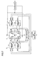
- Fig. 7 is a circuit diagram showing a switching rectifier circuit according to a second embodiment of the invention
- Fig. 8 is a timing chart showing a second switching rectification operation.
- the switching rectifier circuit according to the second embodiment has largely the same configuration as the one according to the first embodiment described previously, and is characterized by the addition of a time constant circuit 19. Accordingly, such circuit elements as find their counterparts in the first embodiment are identified by the same reference signs to omit overlapping description, and given below will be a detailed description of the significance of the addition of the time constant circuit 19 and its operation.
- the output current I is sufficiently large (for example, when the output current I is set for a 500 mA mode), no problem occurs.
- the output current I is small (for example, when the output current I is set for a 100 mA mode)
- the first AC voltage VAC1 or the second AC voltage VAC2 may fail to reach the second threshold voltage (VDC + X2), making it impossible to detect the turning-off timing of the transistor M1 (or M2).
- the switching rectifier circuit is provided with the time constant circuit 19 as a means of forcibly turning the transistor M1 (or M2) off when a predetermined time t3 elapses after the first or second AC voltage VAC1 or VAC2 has increased over the first threshold voltage (VDC + X1), regardless of the first off detection signal DET1b (or the second off detection signal DET2b).
- the time constant circuit 19 turns an off signal OFF to high level, and when the predetermined time t3 elapses thereafter, the time constant circuit 19 turns the off signal OFF to low level.
- the predetermined time t3 may be counted by an analog time counting method using a capacitor and a constant current source, or by a digital time counting method using a clock counter.
- the timing generator 13 Based on the outputs (the first on detection signal DET1a, the first off detection signal DET1b, the second on detection signal DET2a, the second off detection signal DET2b, the third detection signal DET3, the fourth detection signal DET4, and the off signal OFF) of the comparison circuits 121 to 124 and of the time constant circuit 19, the timing generator 13 generates the gate signals G1 to G4 to turn the transistors M1 to M4 on and off.
- the timing generator 13 operates as follows.
- the timing generator 13 turns the gate signal G1 to low level and turns on the transistor M1.
- the timing generator 13 turns the gate signal G1 to high level and turns off the transistor M1.
- the timing generator 13 operates as follows.
- the timing generator 13 increases over the first threshold voltage (VDC + X1) and the second on detection voltage DET2a turns to high level
- the timing generator 13 turns the gate signal G2 to low level and turns on the transistor M2.
- the timing generator 13 turns the gate signal G2 to high level and turns off the transistor M2.
- the predetermined time t3 above be controlled to vary so as to be the shorter the higher the voltage level of the DC voltage VDC. This configuration is usable in applications where the DC voltage VDC varies (as in battery chargers).
- Fig. 9 is a timing chart showing a third switching rectification operation, which is characterized in particular by how the turning on and off of the transistors M3 and M4 is controlled (how the gate signals G3 and G4 are generated).
- the third switching rectification operation may be implemented in both of the configuration according to the first embodiment (see Fig. 3 ) and the configuration according to the second embodiment (see Fig. 7 ).
- the timing generator 13 operates as follows.
- the timing generator 13 turns the gate signal G3 to high level and turns on the transistor M3.
- the timing generator 13 turns the gate signal G3 to low level and turns off the transistor M3.
- the timing generator 13 operates as follows.
- the timing generator 13 turns the gate signal G4 to high level and turns on the transistor M4.
- the timing generator 13 turns the gate signal G4 to low level and turns off the transistor M4.
- Fig. 10 is a timing chart showing a fourth switching rectification operation, which is characterized in particular by how the turning on and off of the transistors M3 and M4 is controlled (how the gate signals G3 and G4 are generated).
- the fourth switching rectification operation may be implemented in both of the configuration according to the first embodiment (see Fig. 3 ) and the configuration according to the second embodiment (see Fig. 7 ).
- the timing generator 13 operates as follows.
- the timing generator 13 turns the gate signal G3 to high level and turns on the transistor M3.
- the timing generator 13 turns the gate signal G3 to low level and turns off the transistor M3.
- the timing generator 13 operates as follows.
- the timing generator 13 turns the gate signal G4 to high level and turns on the transistor M4.
- the timing generator 13 turns the gate signal G4 to low level and turns off the transistor M4.
- Fig. 11 is a timing chart showing a fifth switching rectification operation, which is characterized in particular by how the turning on and off of the transistors M3 and M4 is controlled (how the gate signals G3 and G4 are generated).
- the fifth switching rectification operation may be implemented in both of the configuration according to the first embodiment (see Fig. 3 ) and the configuration according to the second embodiment (see Fig. 7 ).
- the fifth switching rectification operation does not require the detection of the third and fourth detection signals DET3 and DET4, and therefore it is preferable that it be implemented in the third embodiment (see Fig. 12 ) described later, where the comparison circuits 123 and 124 are omitted.
- the timing generator 13 operates as follows.
- the timing generator 13 turns the gate signal G3 to high level and turns on the transistor M3.
- the timing generator 13 turns the gate signal G3 to low level and turns off the transistor M3.
- the gate signal G3 corresponds to the logical inversion of the gate signal G2.
- the timing generator 13 operates as follows.
- the timing generator 13 turns the gate signal G4 to high level and turns on the transistor M4.
- the timing generator 13 turns the gate signal G4 to low level and turns off the transistor M4.
- the gate signal G4 corresponds to the logical inversion of the gate signal G1.
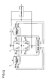
- Fig. 12 is a circuit diagram showing a switching rectifier circuit according to a third embodiment of the invention. Adapted for implementation of the fifth switching rectification operation described above, the switching rectifier circuit according to the third embodiment, compared with the configuration according to the first embodiment, lacks the comparison circuits 123 and 124. Adopting this configuration contributes to reduction in circuit scale.
- Fig. 13 is a circuit diagram showing a switching rectification operation according to a fourth embodiment of the invention.
- the switching rectifier circuit of the fourth embodiment has largely the same configuration as the one according to the first embodiment described previously, and is characterized by the provision of comparison circuits 125 and 126 in place of the comparison circuits 121 and 122 described previously.
- the comparison circuit 125 generates a first detection signal DET1 alone.
- the comparison circuit 122 which generates the second on detection signal DET2a and the second off detection signal DET2b individually
- the comparison circuit 126 generates a second detection signal DET2 alone.
- Fig. 14 is a circuit diagram showing one exemplary configuration of the comparison circuits 125 and 126.
- the comparison circuit 125 includes a hysteresis comparator CMP5
- the comparison circuit 126 includes a hysteresis comparator CMP6.
- the non-inverting input terminal (+) of the hysteresis comparator CMP5 is connected to the terminal to which the first AC voltage VAC1 is applied.
- the inverting input terminal (-) of the hysteresis comparator CMP5 is connected to the terminal to which the DC voltage VDC is applied.
- the hysteresis comparator CMP5 compares the first AC voltage VAC1 with a first threshold voltage (VDC + Y1), which is higher than the DC voltage VDC by a first offset voltage Y1, and with a second threshold voltage (VDC + Y2), which is higher than the DC voltage VDC by a second offset voltage Y2 (where Y2 ⁇ Y1), in order to switch the logic level of the first detection signal DET1.
- the hysteresis comparator CMP5 turns the first detection signal DET1 to high level; when the first AC voltage VAC1 decreases under the second threshold voltage (VDC + Y2), the hysteresis comparator CMP5 turns the first detection signal DET1 to low level.
- the non-inverting input terminal (+) of the hysteresis comparator CMP6 is connected to the terminal to which the second AC voltage VAC2 is applied.
- the inverting input terminal (-) of the hysteresis comparator CMP6 is connected to the terminal to which the DC voltage VDC is applied.
- the hysteresis comparator CMP6 compares the second AC voltage VAC2 with the first threshold voltage (VDC + Y1) and with the second threshold voltage (VDC + Y2), both mentioned above, in order to switch the logic level of the second detection signal DET2.
- the hysteresis comparator CMP6 turns the second detection signal DET2 to high level; when the second AC voltage VAC2 decreases under the second threshold voltage (VDC + Y2), the hysteresis comparator CMP6 turns the second detection signal DET2 to low level.
- the first offset voltage Y1 is set at a voltage level commensurate with the on-state resistance of the transistors M1 and M2 multiplied by the output current I, for example within the range from 5 mV to several tens of mV.
- the second offset voltage Y2 is set within the range from 0 to Y1.
- the logic levels of the first and second detection signals DET1 and DET2 are in no way limited to, but may instead be just the opposite to, those specifically described above in terms of high and low levels.
- the comparison circuits 125 and 126 have the configuration of the comparison circuits 121 and 122 minus the comparators CMP1b and CMP2b. Adopting this configuration helps reduce the circuit scale of the switching rectifier circuit. Moreover, setting the first offset voltage Y1 lower than the first offset voltage X1 mentioned previously helps secure a larger margin in the withstand voltage of the switching rectifier circuit. Moreover, setting the first offset voltage Y1 lower than the first offset voltage X1 mentioned previously also helps shift forward the turning-on timing of the transistors M1 and M2 for increased power efficiency.
- the configuration and operation of the comparison circuit 123 are similar to those in the first embodiment described previously. Specifically, when the first AC voltage VAC1 decreases under the third threshold voltage (VDC - Y3), the comparison circuit 123 turns the third detection signal DET3 to high level; when the first AC voltage VAC1 increases over the fourth threshold voltage (VSS + Y4), the comparison circuit 123 turns the third detection signal DET3 to low level.
- the configuration and operation of the comparison circuit 124 are similar to those in the first embodiment described previously. Specifically, when the second AC voltage VAC2 decreases under the third threshold voltage (VDC - Y3), the comparison circuit 124 turns the fourth detection signal DET4 to high level; when the second AC voltage VAC2 increases over the fourth threshold voltage (VSS + Y4), the comparison circuit 124 turns the fourth detection signal DET4 to low level.
- the third offset voltage Y3 is set within the range from 0.1 V to 0.4 V (lower than the on threshold voltage of the body diodes D3 and D4).
- the fourth offset voltage Y4 is set within the range from VSS (0 V) to VDC.
- the logic levels of the third and fourth detection signals DET3 and DET4 are in no way limited to, but may instead be just the opposite to, those specifically described above in terms of high and low levels.
- Fig. 15 is a timing chart showing a sixth switching rectification operation, and shows plots of, from top down, the first and second AC voltages VAC1 and VAC2, the output current I, the first detection signal DET1, the second detection signal DET2, the third detection signal DET3, the fourth detection signal DET4, and the gate signals G1 to G4.
- the sixth switching rectification operation may be implemented by use of the switching rectifier circuit according to the fourth embodiment (see Fig. 13 ).
- the timing generator 13 operates as follows.
- the timing generator 13 turns the gate signal G1 to low level and turns on the transistor M1.
- the timing generator 13 turns the gate signal G1 to high level and turns off the transistor M1.
- the timing generator 13 operates as follows.
- the timing generator 13 increases over the first threshold voltage (VDC + Y1) and the second detection voltage DET2 turns to high level
- the timing generator 13 turns the gate signal G2 to low level and turns on the transistor M2.
- the timing generator 13 turns the gate signal G2 to high level and turns off the transistor M2.
- the first AC voltage VAC1 increases over the first threshold voltage (VDC + Y1) and the transistor M1 (or M2) is turned on
- the first AC voltage VAC1 drops to close to the DC voltage VDC and momentarily decreases under the second threshold voltage (VDC + Y2).
- the first detection signal DET1 turns to low level unexpectedly.
- the timing generator 13 is configured to ignore a momentary drop in the first and second AC voltage VAC1 and VAC2 under the second threshold voltage (VDC + Y2) when turning on the transistors M1 and M2 respectively.
- the timing generator 13 may be configured to ignore the first detection signal DET1 (or the second detection signal DET2) for a predetermined masking period after the first detection signal DET1 (or the second detection signal DET2) has turned to high level, or may be configured to detect the second low edge that occurs in the first detection signal DET1 (or the second detection signal DET2) after the first detection signal DET1 (or the second detection signal DET2) has turned to high level.
- the timing generator 13 operates as follows. A first wait time t1 after the first AC voltage VAC1 has decreased under the third threshold voltage (VSS - Y3) and the third detection signal DET3 has turned to high level, the timing generator 13 turns the gate signal G3 to high level and turns on the transistor M3. When the second AC voltage VAC2 decreases under the third threshold voltage (VSS - Y3) and the fourth detection signal DET4 turns to high level, the timing generator 13 turns the gate signal G3 to low level and turns off the transistor M3.
- the timing generator 13 operates as follows. A second wait time t2 after the second AC voltage VAC2 has decreased under the third threshold voltage (VSS - Y3) and the fourth detection signal DET4 has turned to high level, then, the timing generator 13 turns the gate signal G4 to high level and turns on the transistor M4. When the first AC voltage VAC1 decreases under the third threshold voltage (VSS - Y3) and the third detection signal DET3 turns to high level, the timing generator 13 turns the gate signal G4 to low level and turns off the transistor M4.
- the first and second wait time t1 and t2 may be equal or different.
- Fig. 16 is a circuit diagram showing a switching rectifier circuit according to a fifth embodiment of the invention
- Fig. 17 is a timing chart showing a seventh switching rectification operation.
- the switching rectifier circuit according to the fifth embodiment has largely the same configuration as the one according to the fourth embodiment described previously, and is characterized by the addition of a time constant circuit 19. Accordingly, such circuit elements as find their counterparts in the first embodiment are identified by the same reference signs as in Fig. 3 to omit overlapping description, and given below will be a detailed description of the significance of the addition of the time constant circuit 19 and its operation.
- the output current I is sufficiently large (for example, when the output current I is set for a 500 mA mode), no problem occurs.
- the output current I is small (for example, when the output current I is set for a 100 mA mode)
- the first AC voltage VAC1 or the second AC voltage VAC2 may fail to reach the second threshold voltage (VDC + Y2), making it impossible to detect the turning-off timing of the transistor M1 (or M2).
- the switching rectifier circuit is provided with the time constant circuit 19 as a means of forcibly turning the transistor M1 (or M2) off when a predetermined time t3 elapses after the first or second AC voltage VAC1 or VAC2 has increased over the first threshold voltage (VDC + Y1), regardless of the first detection signal DET1 (or the second detection signal DET2).
- the time constant circuit 19 turns a mask signal MASK to high level, and when the predetermined time t3 elapses thereafter, the time constant circuit 19 turns the mask signal MASK to low level.
- the reset signal RESET is turned to high level at a rising edge in the third and fourth detection signals DET3 and DET4, and is turned to low level at a rising edge in the first and second detection signals DET1 and DET2.
- the mask signal MASK is used, in the timing generator 13, as a signal for forcibly keeping the transistor M1 (or M2) on for the predetermined time t3.
- the mask signal MASK is used as a signal (an enable signal for securing the minimum on period of the transistor M1 (or M2)) for ignoring an unexpected falling edge in the first detection signal DET1 (or the second detection signal DET2) that occurs when the transistors M1 and M2, respectively, are turned on.
- the predetermined time t3 may be counted by an analog time counting method using a capacitor and a constant current source, or by a digital time counting method using a clock counter.
- the timing generator 13 Based on the outputs (the first detection signal DET1, the second detection signal DET2, the third detection signal DET3, the fourth detection signal DET4, and the mask signal MASK) of the comparison circuits 123 to 126 and of the time constant circuit 19, the timing generator 13 generates the gate signals G1 to G4 to turn the transistors M1 to M4 on and off.
- the timing generator 13 operates as follows.
- the timing generator 13 turns the gate signal G1 to low level and turns on the transistor M1.
- the timing generator 13 turns the gate signal G1 to high level and turns off the transistor M1.
- the timing generator 13 operates as follows.
- the timing generator 13 increases over the first threshold voltage (VDC + Y1) and the second detection voltage DET2 turns to high level
- the timing generator 13 turns the gate signal G2 to low level and turns on the transistor M2.
- the timing generator 13 turns the gate signal G2 to high level and turns off the transistor M2.
- the predetermined time t3 above be controlled to vary so as to be the shorter the higher the voltage level of the DC voltage VDC. This configuration is usable in applications where the DC voltage VDC varies (as in battery chargers). Depending on the application, however, it may be preferable that the predetermined time t3 not vary; accordingly, it is preferable to choose whether to control and vary the predetermined time t3 or keep it at a constant length to suit the situation.
- Fig. 18 is a timing chart showing an eighth switching rectification operation.
- the eighth switching rectification operation can be considered to derive from the seventh switching rectification operation described previously in that it is implemented by use of the switching rectifier circuit according to the fifth embodiment (see Fig. 16 ).
- a difference from the seventh switching rectification operation is that, in the comparison circuits 125 and 126, there are set a first threshold voltage (VDC + Y1), which is higher than the DC voltage VDC, and a second threshold voltage (VDC - Y2), which is lower than the DC voltage VDC.
- the timing generator 13 generates the gate signals G1 to G4 to turn the transistors M1 to M4 on and off.
- the timing generator 13 operates as follows.
- the timing generator 13 turns the gate signal G1 to low level and turns on the transistor M1.
- the timing generator 13 turns the gate signal G1 to high level and turns off the transistor M1.
- the timing generator 13 operates as follows.
- the timing generator 13 increases over the first threshold voltage (VDC + Y1) and the second detection voltage DET2 turns to high level, the timing generator 13 turns the gate signal G2 to low level and turns on the transistor M2.
- the timing generator 13 turns the gate signal G2 to high level and turns off the transistor M2.
- the seventh switching rectification operation is also possible, by using the mask signal MASK, to ignore an unexpected falling edge in the first detection signal DET1 (or the second detection signal DET2) that occurs when the transistors M1 and M2, respectively, are turned on. It is thus possible to secure the minimum on period of the transistor M1 (or M2).
- the present invention is a technology useful in increasing the power conversion efficiency of, for example, switching rectifier circuits incorporated in battery chargers.
Landscapes
- Engineering & Computer Science (AREA)
- Power Engineering (AREA)
- Rectifiers (AREA)
Abstract
Description
- The present invention relates to switching rectifier circuits, and to battery chargers using them.
- Conventionally, as a means of rectifying an AC voltage VAC into a DC voltage VDC, a full-
wave rectification circuit 100 using a diode bridge as shown inFig. 19 is commonly used. Inconveniently, however, thediodes 101 to 104 constituting the diode bridge have a high forward voltage drop, which causes energy loss (power loss or heat generation in thediodes 101 to 104) during the periods in which current I passes through thediodes 101 to 104 (see the hatched areas inFig. 20 ). - As an improvement, there has conventionally been proposed a
switching rectifier circuit 200 in which, as shown inFig. 21 ,diodes 101 to 104 as mentioned above are replaced withtransistors 201 to 204, which are turned on and off with proper timing so as to convert an AC voltage VAC into a DC voltage VDC. - In this
switching rectifier circuit 200, the timing with which the turning on and off of thetransistor 201 is controlled is determined based on the comparison output from a comparator 206 (an output resulting from comparison between the DC voltage VDC and a first AC voltage VAC1); the timing with which the turning on and off of thetransistor 202 is controlled is determined based on the comparison output from a comparator 207 (an output resulting from comparison between the DC voltage VDC and a second AC voltage VAC2). Moreover, the timing with which the turning on and off of thetransistor 203 is controlled is determined based on the comparison output from a comparator 208 (an output resulting from comparison between the reference voltage VSS and the first AC voltage VAC1); the timing with which the turning on and off of thetransistor 204 is controlled is determined based on the comparison output from a comparator 209 (an output resulting from comparison between the reference voltage VSS and the second AC voltage VAC1). - Examples of technologies related to what has been discussed above are found in
Patent Documents - Patent Document 1: Japanese Patent Application Publication No.
H9-131064
Patent Document 2: United States Patent Application Publication No.2009/0016090 - Inconveniently, with the conventional
switching rectifier circuit 200 configured as described above, it is difficult to accurately control the timing with which thetransistors 201 to 204 are turned on and off. Consequently, thetransistors 201 and 204 (or 202 and 203) cannot be turned off reliably before the first AC voltage VAC1 (or the second AC voltage VAC2) decreases under the DC voltage VDC, and this may cause a reverse-flow current from anoutput capacitor 205, leading to diminished power conversion efficiency (seeFig. 22 ). - In view of the above-discussed inconveniences found out by its inventors, the present invention aims to provide a switching rectifier circuit that contributes to higher power conversion efficiency, and to provide a battery charger employing such a switching rectifier circuit.
- To achieve the above object, according to one aspect of the invention, a switching rectification circuit includes: a first switch connected between a terminal to which a first AC voltage is applied and a terminal to which a DC voltage is applied; a second switch connected between a terminal to which a second AC voltage is applied and the terminal to which the DC voltage is applied; a third switch connected between the terminal to which the first AC voltage is applied and a terminal to which a reference voltage is applied; a fourth switch connected between the terminal to which the second AC voltage is applied and the terminal to which the reference voltage is applied; a first comparison circuit adapted to generate from the first AC voltage and the DC voltage a first on detection signal and a first off detection signal individually; a second comparison circuit adapted to generate from the second AC voltage and the DC voltage a second on detection signal and a second off detection signal individually; and a timing generator adapted to control the turning on and off of the first to fourth switches based on at least the outputs of the first and second comparison circuits (a first configuration).
- In the switching rectifier circuit of the first configuration described above, preferably, the first comparison circuit includes: a first hysteresis comparator adapted to turn the first on detection signal to high level or low level when the first AC voltage increases over a first threshold voltage higher than the DC voltage and turn the first on detection signal to low level or high level when the first AC voltage decreases under a third threshold voltage lower than the DC voltage; and a first comparator adapted to turn the first off detection signal to high level or low level when the first AC voltage increases over a second threshold voltage higher than the DC voltage but lower than the first threshold voltage and turn the first off detection signal to low level or high level when the first AC voltage decreases under the second threshold voltage. Moreover, preferably, the second comparison circuit includes: a second hysteresis comparator adapted to turn the second on detection signal to high level or low level when the second AC voltage increases over the first threshold voltage and turn the second on detection signal to low level or high level when the second AC voltage decreases under the third threshold voltage; and a second comparator adapted to turn the second off detection signal to high level or low level when the second AC voltage increases over the second threshold and turn the second off detection signal to low level or high level when the second AC voltage decreases under the second threshold voltage (a second configuration).
- In the switching rectifier circuit of the second configuration described above, preferably, there are further provided: a third comparison circuit adapted to generate from the first AC voltage and the reference voltage a third detection signal; and a fourth comparison circuit adapted to generate from the second AC voltage and the reference voltage a fourth detection signal. Here, preferably, the timing controller is adapted to control the turning on and off of the first to fourth switches based on at least the outputs of the first to fourth comparison circuits (a third configuration).
- In the switching rectifier circuit of the third configuration described above, preferably, the third comparison circuit includes a third hysteresis comparator adapted to turn the third detection signal to high level or low level when the first AC voltage decreases under a fourth threshold voltage lower than the reference voltage and turn the third detection signal to low level or high level when the first AC voltage increases over a fifth threshold voltage higher than the reference voltage, and the fourth comparison circuit includes a fourth hysteresis comparator adapted to turn the fourth detection signal to high level or low level when the second AC voltage decreases under the fourth threshold voltage and turn the fourth detection signal to low level or high level when the second AC voltage increases over the fifth threshold voltage (a fourth configuration).
- In the switching rectifier circuit of the fourth configuration described above, preferably, there is further provided a time constant circuit adapted to generate an enable signal which remains at high level or low level after the first or second AC voltage increases over the first threshold voltage until a predetermined time elapses. Here, preferably, the timing controller is adapted to control the turning on and off of the first to fourth switches based on at least the outputs of the first to fourth comparison circuits and of the time constant circuit (a fifth configuration).
- In the switching rectifier circuit of the fifth configuration described above, preferably, the predetermined time is controlled to vary so as to be the shorter the higher the voltage level of the DC voltage is (a sixth configuration).
- In the switching rectifier circuit of the fourth configuration described above, preferably, the timing generator is adapted to generate the first on and off control signals so as to turn on the first switch when the first AC voltage increases over the first threshold voltage and turn off the first switch when the first AC voltage decreases under the second threshold voltage, generate the second on and off control signals so as to turn on the second switch when the second AC voltage increases over the first threshold voltage and turn off the second switch when the second AC voltage decreases under the second threshold voltage, generate the third on and off control signals so as to turn on the third switch a first wait time after the first AC voltage decreases under the fourth threshold voltage and turn off the third switch when the second AC voltage decreases under the fourth threshold voltage, and generate the fourth on and off control signals so as to turn on the fourth switch a second wait time after the second AC voltage decreases under the fourth threshold voltage and turn off the fourth switch when the first AC voltage decreases under the fourth threshold voltage (a seventh configuration).
- In the switching rectifier circuit of the fifth or sixth configuration described above, preferably, the timing generator is adapted to generate the first on and off control signals so as to turn on the first switch when the first AC voltage increases over the first threshold voltage and turn off the first switch when the first AC voltage decreases under the second threshold voltage or a predetermined time after the first AC voltage has increased over the first threshold voltage, generate the second on and off control signals so as to turn on the second switch when the second AC voltage increases over the first threshold voltage and turn off the second switch when the second AC voltage decreases under the second threshold voltage or a predetermined time after the second AC voltage has increased over the first threshold voltage, generate the third on and off control signals so as to turn on the third switch a first wait time after the first AC voltage decreases under the fourth threshold voltage and turn off the third switch when the second AC voltage decreases under the fourth threshold voltage, and generate the fourth on and off control signals so as to turn on the fourth switch a second wait time after the second AC voltage decreases under the fourth threshold voltage and turn off the fourth switch when the first AC voltage decreases under the fourth threshold voltage (an eighth configuration).
- In the switching rectifier circuit of the fourth configuration described above, preferably, the timing generator is adapted to generate the first on and off control signals so as to turn on the first switch when the first AC voltage increases over the first threshold voltage and turn off the first switch when the first AC voltage decreases under the second threshold voltage, generate the second on and off control signals so as to turn on the second switch when the second AC voltage increases over the first threshold voltage and turn off the second switch when the second AC voltage decreases under the second threshold voltage, generate the third on and off control signals so as to turn on the third switch when the first AC voltage decreases under the fourth threshold voltage and turn off the third switch when the second AC voltage decreases under the second threshold voltage, and generate the fourth on and off control signals so as to turn on the fourth switch when the second AC voltage decreases under the fourth threshold voltage and turn off the fourth switch when the first AC voltage decreases under the second threshold voltage (a ninth configuration).
- In the switching rectifier circuit of the fourth configuration described above, preferably, the timing generator is adapted to generate the first on and off control signals so as to turn on the first switch when the first AC voltage increases over the first threshold voltage and turn off the first switch when the first AC voltage decreases under the second threshold voltage, generate the second on and off control signals so as to turn on the second switch when the second AC voltage increases over the first threshold voltage and turn off the second switch when the second AC voltage decreases under the second threshold voltage, generate the third on and off control signals so as to turn on the third switch when the second AC voltage increases over the first threshold voltage and turn off the third switch when the second AC voltage decreases under the fourth threshold voltage, and generate the fourth on and off control signals so as to turn on the fourth switch when the first AC voltage increases over the first threshold voltage and turn off the fourth switch when the first AC voltage decreases under the fourth threshold voltage (a tenth configuration).
- In the switching rectifier circuit of the second configuration described above, preferably, the timing generator is adapted to generate the first and fourth on and off control signals so as to turn on both the first and fourth switches when the first AC voltage increases over the first threshold voltage and turn off both the first and fourth switches when the first AC voltage decreases under the second threshold voltage, and generate the second and third on and off control signals so as to turn on both the second and third switches when the second AC voltage increases over the first threshold voltage and turn off both the second and third switches when the second AC voltage decreases under the second threshold voltage (an eleventh configuration).
- In the switching rectifier circuit of any one of the seventh to eleventh configurations described above, preferably, the timing generator is adapted to ignore a drop in the first and second AC voltages under the second threshold voltage when turning on the first and second switches respectively (a twelfth configuration).
- According to another aspect of the invention, switching rectification circuit includes: a first switch connected between a terminal to which a first AC voltage is applied and a terminal to which a DC voltage is applied; a second switch connected between a terminal to which a second AC voltage is applied and the terminal to which the DC voltage is applied; a third switch connected between the terminal to which the first AC voltage is applied and a terminal to which a reference voltage is applied; a fourth switch connected between the terminal to which the second AC voltage is applied and the terminal to which the reference voltage is applied; a first comparison circuit adapted to generate from the first AC voltage and the DC voltage a first detection signal; a second comparison circuit adapted to generate from the second AC voltage and the DC voltage a second detection signal; a third comparison circuit adapted to generate from the first AC voltage and the reference voltage a third detection signal; a fourth comparison circuit adapted to generate from the second AC voltage and the reference voltage a fourth detection signal; and a timing generator adapted to control the turning on and off of the first to fourth switches based on at least the outputs of the first to fourth comparison circuits (a thirteenth configuration).
- In the switching rectifier circuit of the thirteenth configuration described above, preferably, the first comparison circuit includes a first hysteresis comparator adapted to turn the first detection signal to high level or low level when the first AC voltage increases over a first threshold voltage higher than the DC voltage and turn the first detection signal to low level or high level when the first AC voltage decreases under a second threshold voltage higher than the DC voltage but lower than the first threshold voltage, the second comparison circuit includes a second hysteresis comparator adapted to turn the second detection signal to high level or low level when the second AC voltage increases over the first threshold voltage and turn the second detection signal to low level or high level when the second AC voltage decreases under the second threshold voltage, the third comparison circuit includes a third hysteresis comparator adapted to turn the third detection signal to high level or low level when the first AC voltage decreases under a third threshold voltage lower than the reference voltage and turn the third detection signal to low level or high level when the first AC voltage increases over a fourth threshold voltage higher than the reference voltage, and the fourth comparison circuit includes a fourth hysteresis comparator adapted to turn the fourth detection signal to high level or low level when the second AC voltage decreases under the third threshold voltage and turn the fourth detection signal to low level or high level when the second AC voltage increases over the fourth threshold voltage (a fourteenth configuration).
- In the switching rectifier circuit of the thirteenth configuration described above, preferably, the first comparison circuit includes a first hysteresis comparator adapted to turn the first detection signal to high level or low level when the first AC voltage increases over a first threshold voltage higher than the DC voltage and turn the first detection signal to low level or high level when the first AC voltage decreases under a second threshold voltage lower than the DC voltage, the second comparison circuit includes a second hysteresis comparator adapted to turn the second detection signal to high level or low level when the second AC voltage increases over the first threshold voltage and turn the second detection signal to low level or high level when the second AC voltage decreases under the second threshold voltage, the third comparison circuit includes a third hysteresis comparator adapted to turn the third detection signal to high level or low level when the first AC voltage decreases under a third threshold voltage lower than the reference voltage and turn the third detection signal to low level or high level when the first AC voltage increases over a fourth threshold voltage higher than the reference voltage, and the fourth comparison circuit includes a fourth hysteresis comparator adapted to turn the fourth detection signal to high level or low level when the second AC voltage decreases under the third threshold voltage and turn the fourth detection signal to low level or high level when the second AC voltage increases over the fourth threshold voltage (a fifteenth configuration).
- In the switching rectifier circuit of the fourteenth or fifteenth configuration described above, preferably, there is further provided a time constant circuit adapted to generate a mask signal which remains at high level or low level after the first or second AC voltage increases over the first threshold voltage until a predetermined time elapses. Here, preferably, the timing controller is adapted to control the turning on and off of the first to fourth switches based on at least the outputs of the first to fourth comparison circuits and of the time constant circuit (a sixteenth configuration).
- In the switching rectifier circuit of the sixteenth configuration described above, preferably, the predetermined time is controlled to vary so as to be the shorter the higher the voltage level of the DC voltage is (a seventeenth configuration).
- In the switching rectifier circuit of the fourteenth or fifteenth configuration described above, preferably, the timing generator is adapted to generate the first on and off control signals so as to turn on the first switch when the first AC voltage increases over the first threshold voltage and turn off the first switch when the first AC voltage decreases under the second threshold voltage, generate the second on and off control signals so as to turn on the second switch when the second AC voltage increases over the first threshold voltage and turn off the second switch when the second AC voltage decreases under the second threshold voltage, generate the third on and off control signals so as to turn on the third switch a first wait time after the first AC voltage decreases under the third threshold voltage and turn off the third switch when the second AC voltage decreases under the third threshold voltage, and generate the fourth on and off control signals so as to turn on the fourth switch a second wait time after the second AC voltage decreases under the third threshold voltage and turn off the fourth switch when the first AC voltage decreases under the third threshold voltage (an eighteenth configuration).
- In the switching rectifier circuit of the sixteenth or seventeenth configuration described above, preferably, the timing generator is adapted to generate the first on and off control signals so as to turn on the first switch when the first AC voltage increases over the first threshold voltage and turn off the first switch when the first AC voltage decreases under the second threshold voltage or a predetermined time after the first AC voltage has increased over the first threshold voltage, generate the second on and off control signals so as to turn on the second switch when the second AC voltage increases over the first threshold voltage and turn off the second switch when the second AC voltage decreases under the second threshold voltage or a predetermined time after the second AC voltage has increased over the first threshold voltage, generate the third on and off control signals so as to turn on the third switch a first wait time after the first AC voltage decreases under the third threshold voltage and turn off the third switch when the second AC voltage decreases under the third threshold voltage, and generate the fourth on and off control signals so as to turn on the fourth switch a second wait time after the second AC voltage decreases under the third threshold voltage and turn off the fourth switch when the first AC voltage decreases under the third threshold voltage (a nineteenth configuration).
- In the switching rectifier circuit of the eighteenth or nineteenth configuration described above, preferably, the timing generator is adapted to ignore a drop in the first and second AC voltages under the second threshold voltage when turning on the first and second switches respectively (a twentieth configuration).
- In the switching rectifier circuit of any one of the first to twentieth configuration described above, preferably, the first to fourth switches are all field-effect transistors (a twenty-first configuration).
- In the switching rectifier circuit of the twenty-first configuration described above, preferably, the timing controller is adapted to keep the first to fourth switches all off until the DC voltage reaches a predetermined level and rectify the AC voltages into the DC voltage through rectification operation using body diodes of the first to fourth switches respectively (a twenty-second configuration).
- According to yet another aspect of the invention, a battery charger includes the switching rectifier circuit according to any one of the first to twenty-second configurations described above, and the controls the charging of a battery cell by using the DC voltage (a twenty-third configuration).
- In the battery charger according to the twenty-third configuration described above, there may be further provided a transformer coupling between a commercial AC power source and the switching rectifier circuit on a non-contact basis (a twenty-fourth configuration).
- According to the present invention, it is possible to provide a switching rectifier circuit that contributes to higher power conversion efficiency, and to provide a battery charger employing such a switching rectifier circuit
-
-
Fig. 1 is a block diagram showing one exemplary configuration of a battery charger according to the invention; -
Fig. 2A is a circuit diagram illustrating switching rectification operation (in a first operation state); -
Fig. 2B is a circuit diagram illustrating switching rectification operation (in a second operation state); -
Fig. 3 is a circuit diagram showing a switching rectifier circuit according to a first embodiment of the invention; -
Fig. 4 is a circuit diagram showing one exemplary configuration ofcomparators -
Fig. 5 is a circuit diagram showing one exemplary configuration ofcomparators -
Fig. 6 is a timing chart showing a first switching rectification operation; -
Fig. 7 is a circuit diagram showing a switching rectifier circuit according to a second embodiment of the invention; -
Fig. 8 is a timing chart showing a second switching rectification operation; -
Fig. 9 is a timing chart showing a third switching rectification operation; -
Fig. 10 is a timing chart showing a fourth switching rectification operation; -
Fig. 11 is a timing chart showing a fifth switching rectification operation; -
Fig. 12 is a circuit diagram showing a switching rectifier circuit according to a third embodiment of the invention; -
Fig. 13 is a circuit diagram showing a switching rectifier circuit according to a fourth embodiment of the invention; -
Fig. 14 is a circuit diagram showing one exemplary configuration ofcomparators -
Fig. 15 is a timing chart showing a sixth switching rectification operation; -
Fig. 16 is a circuit diagram showing a switching rectifier circuit according to a fifth embodiment of the invention; -
Fig. 17 is a timing chart showing a seventh switching rectification operation; -
Fig. 18 is a timing chart showing an eighth switching rectification operation; -
Fig. 19 is a circuit diagram showing a first conventional example of a rectification circuit; -
Fig. 20 is a timing chart showing how energy loss occurs; -
Fig. 21 is a circuit diagram showing a second conventional example of a rectification circuit; and -
Fig. 22 is a timing chart showing how a reverse-flow current occurs. - Hereinafter, the present invention will be described in detail by way of exemplary configurations where it is applied to a switching rectifier circuit incorporated in a battery charger.
-
Fig. 1 is a block diagram showing an exemplary configuration of a battery charger according to the invention. Thebattery charger 1 of this exemplary configuration includes a switchingrectifier IC 10, atransformer 20, amicroprocessor 30, and aload modulator 40, and controls the charging of a battery cell 3 by use of a DC (direct-current) voltage VDC obtained by rectifying on a full-wave basis an AC (alternating-current) voltage VAC from a commercialAC power source 2. - The switching
rectifier IC 10 has integrated into it anH bridge 11, adiscriminator 12, atiming generator 13, an undervoltage detector 14 (UVLO, undervoltage lock-out), aprotection circuit 15, an overvoltage detector 16 (OVP, overvoltage protection), an abnormal temperature detector 17 (TSD, thermal shutdown), and aswitch 18. Connected to the switchingrectifier IC 10 externally to it are thetransformer 20, themicroprocessor 30, theload modulator 40, the battery cell 3, and discrete components such as an output capacitor C1. The configuration of the switchingrectifier IC 10 will be described in detail later. - The
transformer 20 serves as a means of connecting between the commercialAC power source 2 and the switchingrectifier IC 1 on a non-contact basis, and has a primary coil L1 and a secondary coil L2. - The
microprocessor 30 receives a DC voltage VDC from the switchingrectifier IC 10, and operates to monitor the battery voltage VBATT, generate a switch signal SW, generate a modulation input signal MODIN, and otherwise. - The
load modulator 40 transfers the modulation input signal MODIN fed from themicroprocessor 30 to the primary side via thetransformer 20. - The
H bridge 11 is composed of P-channel MOS field-effect transistors M1 and M2 and N-channel MOS field-effect transistors M3 and M4 connected in an H bridge configuration. - The source and backgate of the transistor M1 are both connected to a terminal to which the DC voltage VDC is applied. The drain of the transistor M1 is connected to a terminal to which a first AC voltage VAC1 (the AC voltage appearing at a first end of the secondary coil L2) is applied. The gate of the transistor M1 is connected to the timing generator 13 (specifically, to a terminal to which a first gate signal G1 is output). Thus, the transistor M1 corresponds to a first switch connected between the terminals to which the first AC voltage VAC1 and the DC voltage VDC, respectively, are applied.
- The source and backgate of the transistor M2 are both connected to the terminal to which the DC voltage VDC is applied. The drain of the transistor M2 is connected to a terminal to which a second AC voltage VAC2 (the AC voltage appearing at a second end of the secondary coil L2) is applied. The gate of the transistor M2 is connected to the timing generator 13 (specifically, to a terminal to which a second gate signal G2 is output). Thus, the transistor M2 corresponds to a second switch connected between the terminals to which the second AC voltage VAC2 and the DC voltage VDC, respectively, are applied.
- The source and backgate of the transistor M3 are both connected to a terminal to which a reference voltage VSS (in
Fig. 1 , a ground voltage PGND) is applied. The drain of the transistor M3 is connected to the terminal to which the first AC voltage VAC1 is applied. The gate of the transistor M3 is connected to the timing generator 13 (specifically, to a terminal to which a third gate signal G3 is output). Thus, the transistor M3 corresponds to a third switch connected between the terminals to which the first AC voltage VAC1 and the reference voltage VSS, respectively, are applied. - The source and backgate of the transistor M4 are both connected to the terminal to which the reference voltage VSS is applied. The drain of the transistor M4 is connected to the terminal to which the second AC voltage VAC2 is applied. The gate of the transistor M4 is connected to the timing generator 13 (specifically, to a terminal to which a fourth gate signal G4 is output). Thus, the transistor M4 corresponds to a fourth switch connected between the terminals to which the second AC voltage VAC2 and the reference voltage VSS, respectively, are applied.
- It is preferable to use as the transistors M1 to M4 power-path MOS FETs with a low on-state resistance.
- The
discriminator 12 compares each of the first and second AC voltages VAC1 and VAC2 with each of the DC voltage VDC and the reference voltage VSS, generates detection signals reflecting the results of the comparisons, and feeds them to thetiming generator 13. The specific circuit configuration and operation of thediscriminator 12 will be described in detail later. - The
timing generator 13 turns on and off the transistors M1 to M4 based on the detection signals fed from thediscriminator 12. Thetiming generator 13 also has the function of stopping the rectification operation by turning the transistors M1 to M4 all off, or by turning the transistors M3 and M4 both on and thereby short-circuiting both ends of the primary coil L1, based on an undervoltage protection signal fed from the undervoltage detector 14 and a fault protection signal fed from theprotection circuit 15. The specific operation of thetiming generator 13 will be described in detail later. - The undervoltage detector 14 generates an undervoltage protection signal which indicates whether or not the DC voltage VDC is equal to or higher than a predetermined level, and feeds it to the
timing generator 13. Based on the undervoltage protection signal, thetiming generator 13 keeps the transistors M1 to M4 all off until the DC voltage VDC reaches the predetermined level. Specifically, until the DC voltage VDC reaches the predetermined level, the switchingrectifier IC 10 rectifies the AC voltage VAC into the DC voltage VDC through rectification operation using the body diodes D1 to D4 (seeFigs. 2A, 2B ,3 , etc.) parasitic to the transistors M1 to M4 respectively. - Based on an overvoltage detection signal fed from the
overvoltage detector 16 and an abnormal temperature detection signal fed from theabnormal temperature detector 17, theprotection circuit 15 generates a fault protection signal which indicates whether or not there is some fault in the switchingrectifier IC 10, and feeds it to thetiming generator 13. When thetiming generator 13 recognizes that there is some fault in the switchingrectifier IC 10 based on the fault protection signal, it forcibly stops the transistors M1 to M4. - The
overvoltage detector 16 generates an overvoltage detection signal which indicates whether or not the DC voltage VDC is equal to or higher than a predetermined level, and feeds it to theprotection circuit 15. - The
abnormal temperature detector 17 generates an abnormal temperature detection signal which indicates whether or not the internal temperature of the switchingrectifier IC 10 equal to or higher than a predetermined level, and feeds it to theprotection circuit 15. - A first terminal of the
switch 18 is connected to a terminal to which the battery voltage VBATT is applied. A second terminal of theswitch 18 is connected to the terminal to which the DC voltage VDC is applied. The control terminal of theswitch 18 is connected to a terminal to which the switch signal SW is fed. - A switching rectifier circuit that rectifies the AC voltage VAC on a full-wave basis to produce the DC voltage VDC is constituted by, of the components mentioned above, the
H bridge 11, thediscriminator 12, thetiming generator 13, and the output capacitor C1 in particular. -
Figs. 2A and 2B are circuit diagrams illustrating switching rectification operation. In a state where the transistors M1 and M4 are on and the transistors M2 and M3 are off, current I passes through the path shown inFig. 2A , and the output capacitor C1 is charged. On the other hand, in a state where the transistors M1 and M4 are off and the transistors M2 and M3 are on, current I passes through the path shown inFig. 2B , and the output capacitor C1 is charged. Through this switching control, the AC voltage VAC is rectified on a full-wave basis into the DC voltage VDC. In a state where the transistors M1 to M4 are all off, the AC voltage VAC is rectified into the DC voltage VDC through rectification operation using the body diodes D1 to D4. -
Fig. 3 is a circuit diagram of a switching rectifier circuit according to a first embodiment of the invention. The switching rectifier circuit according to the first embodiment has, as thediscriminator 12,comparison circuits 121 to 124. Thecomparison circuit 121 receives the first AC voltage VAC and the DC voltage VDC, and generates a first on detection signal DET1a and a first off detection signal DEX1b individually. Thecomparison circuit 122 receives the second AC voltage VAC and the DC voltage VDC, and generates a second on detection signal DET2a and a second off detection signal DET2b individually. Thecomparison circuit 123 receives the first AC voltage VAC and the reference voltage VSS, and generates a third detection signal DET3. Thecomparison circuit 124 receives the second AC voltage VAC2 and the reference voltage VSS, and generates a fourth detection signal DET4. -
Fig. 4 is a circuit diagram showing one exemplary configuration of thecomparison circuits comparison circuit 121 includes a hysteresis comparator CMP1a and a comparator CMP1b, and thecomparison circuit 122 includes a hysteresis comparator CMP2a and a comparator CMP2b. - The non-inverting input terminal (+) of the hysteresis comparator CMP1a is connected to the terminal to which the first AC voltage VAC1 is applied. The inverting input terminal (-) of the hysteresis comparator CMP1a is connected to the terminal to which the DC voltage VDC is applied. The hysteresis comparator CMP1a is configured to compare the first AC voltage VAC1 with a first threshold voltage (VDC + X1), which is higher than the DC voltage VDC by a first offset voltage X1, and with a third threshold voltage (VDC - X3), which is lower than the DC voltage VDC by a third offset voltage X3, in order to switch the logic level of the first on detection signal DET1a. Specifically, when the first AC voltage VAC1 increases over the first threshold voltage (VDC + X1), the hysteresis comparator CMP1a turns the first on detection signal DET1a to high level; when the first AC voltage VAC1 decreases under the third threshold voltage (VDC - X3), the hysteresis comparator CMP1a turns the first on detection signal DET1a to low level.
- The non-inverting input terminal (+) of the comparator CMP1b is connected to the terminal to which the first AC voltage VAC1 is applied. The inverting input terminal (-) of the comparator CMP1b is connected to the terminal to which the DC voltage VDC is applied. The comparator CMP1b is configured to compare the first AC voltage VAC1 with a second threshold voltage (VDC + X2), which is higher than the DC voltage VDC but lower than the first threshold voltage (VDC + X1), to switch the logic level of the first off detection signal DET1b. Specifically, when the first AC voltage VAC1 increases over the second threshold voltage (VDC + X2), the comparator CMP1b turns the first off detection signal DET1b to high level; when the first AC voltage VAC1 decreases under the second threshold voltage (VDC + X2), the comparator CMP1b turns the first off detection signal DET1b to low level.
- The non-inverting input terminal (+) of the hysteresis comparator CMP2a is connected to the terminal to which the second AC voltage VAC2 is applied. The inverting input terminal (-) of the hysteresis comparator CMP2a is connected to the terminal to which the DC voltage VDC is applied. The hysteresis comparator CMP2a is configured to compare the second AC voltage VAC2 with the first threshold voltage (VDC + X1) and with the third threshold voltage, both mentioned above, in order to switch the logic level of the second on detection signal DET2a. Specifically, when the second AC voltage VAC2 increases over the first threshold voltage (VDC + X1), the hysteresis comparator CMP2a turns the second on detection signal DET2a to high level; when the second AC voltage VAC2 decreases under the third threshold voltage (VDC - X3), the hysteresis comparator CMP2a turns the second on detection signal DET2a to low level.
- The non-inverting input terminal (+) of the comparator CMP2b is connected to the terminal to which the second AC voltage VAC2 is applied. The inverting input terminal (-) of the comparator CMP2b is connected to the terminal to which the DC voltage VDC is applied. The comparator CMP2b is configured to compare the second AC voltage VAC2 with the second threshold voltage (VDC + X2), mentioned above, to switch the logic level of the second off detection signal DET2b. Specifically, when the second AC voltage VAC2 increases over the second threshold voltage (VDC + X2), the comparator CMP2b turns the second off detection signal DET2b to high level; when the second AC voltage VAC2 decreases under the second threshold voltage (VDC + X2), the comparator CMP2b turns the second off detection signal DET2b to low level.
- Preferably, the first offset voltage X1 is set within the range from 0.1 V to 0.4 V (lower than the on threshold voltage of the body diodes D1 and D2). Preferably, the second offset voltage X2 is set within the range from 0 to X1 (more specifically, at a voltage level commensurate with the on-state resistance of the transistors M1 and M2 multiplied by the output current I, for example in the range from 10 mV to 20 mV). Preferably, the third offset voltage X3 is set within the range from VSS (0 V) to VDC.
- The logic levels of the first on detection signal DET1a, the first off detection signal DET1b, the second on detection signal DET2a, and the second off detection signal are in no way limited to, but may instead be just the opposite to, those specifically described above in terms of high and low levels.
- As described above, the
comparison circuit 121 is configured to have separately the hysteresis comparator CMP1a for generating the first on detection signal DET1a and the comparator CMP1b for generating the first off detection signal DET1b, and thecomparison circuit 122 is configured to have separately the hysteresis comparator CMP2a for generating the second on detection signal DET2a and the comparator CMP2b for generating the second off detection signal DET2b. - Owing to the adoption of the configuration described above, it is possible to accurately set both the first threshold voltage (VDC + X1) and the second threshold voltage (VDC + X2), and thus it is possible to increase the accuracy with which the transistors M1 and M2 are turned on and off by the
timing generator 13. Accordingly, with a switching rectifier circuit according to this embodiment, it is possible, with minimal operation of the body diodes D1 to D4 parasitic to the transistors M1 to M4, to reliably prevent a reverse flow of the output current I, and this helps increase the power conversion efficiency of the switching rectifier circuit. -
Fig. 5 is a circuit diagram showing one exemplary configuration of thecomparison circuits comparison circuit 123 includes a hysteresis comparator CMP3, and thecomparison circuit 124 includes a hysteresis comparator CMP4. - The non-inverting input terminal (+) of the hysteresis comparator CMP3 is connected to the terminal to which the reference voltage VSS is applied. The inverting input terminal (-) of the hysteresis comparator CMP3 is connected to the terminal to which the first AC voltage VAC1 is applied. The hysteresis comparator CMP3 is configured to compare the first AC voltage VAC1 with a fourth threshold voltage (VSS - X4), which is lower than the reference voltage VSS by a fourth offset voltage X4, and with a fifth threshold voltage (VSS + X5), which is higher than the reference voltage VSS by a fifth offset voltage X5, in order to switch the logic level of the third detection signal DET3. Specifically, when the first AC voltage VAC1 decreases under the fourth threshold voltage (VSS - X4), the hysteresis comparator CMP3 turns the third detection signal DET3 to high level; when the first AC voltage VAC1 increases over the fifth threshold voltage, the hysteresis comparator CMP3 turns the third detection signal DET3 to low level.
- The non-inverting input terminal (+) of the hysteresis comparator CMP4 is connected to the terminal to which the reference voltage VSS is applied. The inverting input terminal (-) of the hysteresis comparator CMP4 is connected to the terminal to which the second AC voltage VAC2 is applied. The hysteresis comparator CMP4 is configured to compare the second AC voltage VAC2 with the fourth threshold voltage (VSS - X4) and with the fifth threshold voltage (VSS + X5), both mentioned above, in order to switch the logic level of the fourth detection signal DET4. Specifically, when the second AC voltage VAC2 decreases under the fourth threshold voltage (VSS - X4), the hysteresis comparator CMP4 turns the fourth detection signal DET4 to high level; when the second AC voltage VAC2 increases over the fifth threshold voltage, the hysteresis comparator CMP4 turns the fourth detection signal DET4 to low level.
- Preferably, the fourth offset voltage X4 is set within the range from 0.1 V to 0.4 V (lower than the on threshold voltage of the body diodes D3 and D4). Preferably, the fifth offset voltage X5 is set within the range from VSS (0 V) to VDC.
- The logic levels of the third and fourth detection signals DET3 and DET4 are in no way limited to, but may instead be just the opposite to, those specifically described above in terms of high and low levels.
- Based on the outputs from the
comparison circuits 121 to 124 (the first on detection signal DET1a, the first off detection signal DET1b, the second on detection signal DET2a, the second off detection signal DET2b, the third detection signal DET3, and the fourth detection signal DET4), thetiming generator 13 generates gate signals G1 to G4 to turn the transistors M1 to M4 on and off. -
Fig. 6 is a timing chart showing a first switching rectification operation, and shows plots of, from top down, the first and second AC voltages VAC1 and VAC2, the output current I, the first on detection signal DET1a, the first off detection signal DET1b, the second on detection signal DET2a, the second off detection signal DET2b, the third detection signal DET3, the fourth detection signal DET4, and the gate signals G1 to G4. - With respect to the turning on and off of the transistor M1, the
timing generator 13 operates as follows. When the first AC voltage VAC1 increases over the first threshold voltage (VDC + X1) and the first on detection voltage DET1a turns to high level, thetiming generator 13 turns the gate signal G1 to low level and turns on the transistor M1. When the first AC voltage VAC1 decreases under the second threshold voltage (VDC + X2) and the first off detection signal DET1b turns to low level, thetiming generator 13 turns the gate signal G1 to high level and turns off the transistor M1. - Likewise, with respect to the turning on and off of the transistor M2, the
timing generator 13 operates as follows. When the second AC voltage VAC2 increases over the first threshold voltage (VDC + X1) and the second on detection voltage DET2a turns to high level, thetiming generator 13 turns the gate signal G2 to low level and turns on the transistor M2. When the second AC voltage VAC2 decreases under the second threshold voltage (VDC + X2) and the second off detection signal DET2b turns to low level, thetiming generator 13 turns the gate signal G2 to high level and turns off the transistor M2. - Inconveniently, when the first AC voltage VAC1 (or the second AC voltage VAC2) increases over the first threshold voltage (VDC + X1) and the transistor M1 (or M2) is turned on, the first AC voltage VAC1 (or the second AC voltage VAC2) drops to close to the DC voltage VDC and momentarily decreases under the second threshold voltage (VDC + X2). Thus, immediately after the transistor M1 (or M2) is turned on, the first off detection signal DET1b (or the second off detection signal DET2b) turns to low level unexpectedly.
- To avoid that, the
timing generator 13 is configured to ignore a momentary drop in the first and second AC voltage VAC1 and VAC2 under the second threshold voltage (VDC + X2) when turning on the transistors M1 and M2 respectively. For example, thetiming generator 13 may be configured to ignore the first off detection signal DET1b (or the second off detection signal DET2b) for a predetermined masking period after the first on detection signal DET1a (or the second on detection signal DET2a) has turned to high level, or may be configured to detect the second low edge that occurs in the first off detection signal DET1b (or the second off detection signal DET2b) after the first on detection signal DET1a (or the second on detection signal DET2a) has turned to high level. - With this configuration, it is possible to prevent the transistor M1 (or M2) from being turned off unnecessarily by being triggered by an unexpected low edge in the first off detection signal DET1b (or the second off detection signal DET2b).
- With respect to the turning on and off of the transistor M3, the
timing generator 13 operates as follows. A first wait time t1 after the first AC voltage VAC1 has decreased under the fourth threshold voltage (VSS - X4) and the third detection signal DET3 has turned to high level, thetiming generator 13 turns the gate signal G3 to high level and turns on the transistor M3. When the second AC voltage VAC2 decreases under the fourth threshold voltage (VSS - X4) and the fourth detection signal DET4 turns to high level, thetiming generator 13 turns the gate signal G3 to low level and turns off the transistor M3. - Likewise, with respect to the turning on and off of the transistor M4, the
timing generator 13 operates as follows. A second wait time t2 after the second AC voltage VAC2 has decreased under the fourth threshold voltage (VSS - X4) and the fourth detection signal DET4 has turned to high level, then, thetiming generator 13 turns the gate signal G4 to high level and turns on the transistor M4. When the first AC voltage VAC1 decreases under the fourth threshold voltage (VSS - X4) and the third detection signal DET3 turns to high level, thetiming generator 13 turns the gate signal G4 to low level and turns off the transistor M4. - With this configuration where the transistor M3 is turned on the first wait time t1 after the transistor M4 has been turned off and the transistor M4 is turned off the second wait time t2 after the transistor M3 has been turned off, it is possible to reliably prevent the transistors M3 and M4 from turning on simultaneously. The first and second wait time t1 and t2 may be equal or different.
- With the switching rectification operation described above, it is possible, with minimal operation of the body diodes D1 to D4 parasitic to the transistors M1 to M4, to reliably prevent a reverse flow of the output current I, and this helps increase the power conversion efficiency of the switching rectifier circuit.
-
Fig. 7 is a circuit diagram showing a switching rectifier circuit according to a second embodiment of the invention, andFig. 8 is a timing chart showing a second switching rectification operation. As shown inFig. 7 , the switching rectifier circuit according to the second embodiment has largely the same configuration as the one according to the first embodiment described previously, and is characterized by the addition of a timeconstant circuit 19. Accordingly, such circuit elements as find their counterparts in the first embodiment are identified by the same reference signs to omit overlapping description, and given below will be a detailed description of the significance of the addition of the timeconstant circuit 19 and its operation. - In a case where the output current I is sufficiently large (for example, when the output current I is set for a 500 mA mode), no problem occurs. In a case where the output current I is small (for example, when the output current I is set for a 100 mA mode), as shown in
Fig. 8 , after the transistor M1 (or M2) is turned on, the first AC voltage VAC1 (or the second AC voltage VAC2) may fail to reach the second threshold voltage (VDC + X2), making it impossible to detect the turning-off timing of the transistor M1 (or M2). - To avoid that, the switching rectifier circuit according to this embodiment is provided with the time
constant circuit 19 as a means of forcibly turning the transistor M1 (or M2) off when a predetermined time t3 elapses after the first or second AC voltage VAC1 or VAC2 has increased over the first threshold voltage (VDC + X1), regardless of the first off detection signal DET1b (or the second off detection signal DET2b). - At the same time that a reset signal RESET (for example, the AND signal of the first and second on detection signals DET1a and DET2a) fed from the
timing generator 13 is turned to high level, the timeconstant circuit 19 turns an off signal OFF to high level, and when the predetermined time t3 elapses thereafter, the timeconstant circuit 19 turns the off signal OFF to low level. The predetermined time t3 may be counted by an analog time counting method using a capacitor and a constant current source, or by a digital time counting method using a clock counter. - Based on the outputs (the first on detection signal DET1a, the first off detection signal DET1b, the second on detection signal DET2a, the second off detection signal DET2b, the third detection signal DET3, the fourth detection signal DET4, and the off signal OFF) of the
comparison circuits 121 to 124 and of the timeconstant circuit 19, thetiming generator 13 generates the gate signals G1 to G4 to turn the transistors M1 to M4 on and off. - Specifically, with respect to the turning on and off of the transistor M1, the
timing generator 13 operates as follows. When the first AC voltage VAC1 increases over the first threshold voltage (VDC + X1) and the first on detection voltage DEM1a turns to high level, thetiming generator 13 turns the gate signal G1 to low level and turns on the transistor M1. When the first AC voltage VAC1 decreases under the second threshold voltage (VDC + X2) and the first off detection signal DET1b turns to low level, or when the off signal OFF turns to low level the predetermined time t3 after the first AC voltage VAC1 has increased over the first threshold voltage (VDC + X1), thetiming generator 13 turns the gate signal G1 to high level and turns off the transistor M1. - Likewise, with respect to the turning on and off of the transistor M2, the
timing generator 13 operates as follows. When the second AC voltage VAC2 increases over the first threshold voltage (VDC + X1) and the second on detection voltage DET2a turns to high level, thetiming generator 13 turns the gate signal G2 to low level and turns on the transistor M2. When the second AC voltage VAC2 decreases under the second threshold voltage (VDC + X2) and the second off detection signal DET2b turns to low level, or when the off signal OFF turns to low level the predetermined time t3 after the second AC voltage VAC2 has increased over the first threshold voltage (VDC + X1), thetiming generator 13 turns the gate signal G2 to high level and turns off the transistor M2. - The turning on and off of the transistors M3 and M4 is handled in a similar manner as in the first embodiment described previously (the first switching rectification operation (
Fig. 6 )), and therefore no overlapping description will be repeated. - With this configuration, even if, after the transistor M1 (or M2) is turned on, the first AC voltage VAC1 (or the second AC voltage VAC2) does not reach the second threshold voltage (VDC + X2), regardless of the first off detection signal DET1b (or the second off detection signal DET2b), it is possible, by using the off signal OFF, to forcibly turn off the transistor M1 (or M2). It is thus possible to prevent a reverse flow of the output current I.
- It is preferable that the predetermined time t3 above be controlled to vary so as to be the shorter the higher the voltage level of the DC voltage VDC. This configuration is usable in applications where the DC voltage VDC varies (as in battery chargers).
-
Fig. 9 is a timing chart showing a third switching rectification operation, which is characterized in particular by how the turning on and off of the transistors M3 and M4 is controlled (how the gate signals G3 and G4 are generated). The third switching rectification operation may be implemented in both of the configuration according to the first embodiment (seeFig. 3 ) and the configuration according to the second embodiment (seeFig. 7 ). - With respect to the turning on and off of the transistor M3, the
timing generator 13 operates as follows. When the first AC voltage VAC1 decreases under the fourth threshold voltage (VSS - X4) and the third detection signal DET3 turns to high level, thetiming generator 13 turns the gate signal G3 to high level and turns on the transistor M3. When the second AC voltage VAC2 decreases under the second threshold voltage (VDC + X2) and the second off detection signal DET2b turns to low level, thetiming generator 13 turns the gate signal G3 to low level and turns off the transistor M3. - Likewise, with respect to the turning on and off of the transistor M4, the
timing generator 13 operates as follows. When the second AC voltage VAC2 decreases under the fourth threshold voltage (VSS - X4) and the fourth detection signal DET4 turns to high level, thetiming generator 13 turns the gate signal G4 to high level and turns on the transistor M4. When the first AC voltage VAC1 decreases under the second threshold voltage (VDC + X2) and the first off detection signal DET1b turns to low level, thetiming generator 13 turns the gate signal G4 to low level and turns off the transistor M4. - The turning on and off of the transistors M1 and M2 is handled in a similar manner as in the first embodiment described previously, and therefore no overlapping description will be repeated.
- Also with the third switching rectification operation described above, as with the first and second switching rectification operations described previously, it is possible, with minimal operation of the body diodes D1 to D4 parasitic to the transistors M1 to M4, to reliably prevent a reverse flow of the output current I, and this helps increase the power conversion efficiency of the switching rectifier circuit.
-
Fig. 10 is a timing chart showing a fourth switching rectification operation, which is characterized in particular by how the turning on and off of the transistors M3 and M4 is controlled (how the gate signals G3 and G4 are generated). The fourth switching rectification operation may be implemented in both of the configuration according to the first embodiment (seeFig. 3 ) and the configuration according to the second embodiment (seeFig. 7 ). - With respect to the turning on and off of the transistor M3, the
timing generator 13 operates as follows. When the second AC voltage VAC2 increases over the first threshold voltage (VDC + X1) and the second on detection signal DET2a turns to high level, thetiming generator 13 turns the gate signal G3 to high level and turns on the transistor M3. When the second AC voltage VAC2 decreases under the fourth threshold voltage (VSS - X4) and the fourth detection signal DET4 turns to high level, thetiming generator 13 turns the gate signal G3 to low level and turns off the transistor M3. - Likewise, with respect to the turning on and off of the transistor M4, the
timing generator 13 operates as follows. When the first AC voltage VAC1 increases over the first threshold voltage (VDC + X1) and the first on detection signal DET1a turns to high level, thetiming generator 13 turns the gate signal G4 to high level and turns on the transistor M4. When the first AC voltage VAC1 decreases under the fourth threshold voltage (VSS - X4) and the third detection signal DET3 turns to high level, thetiming generator 13 turns the gate signal G4 to low level and turns off the transistor M4. - The turning on and off of the transistors M1 and M2 is handled in a similar manner as in the first embodiment described previously, and therefore no overlapping description will be repeated.
- Also with the fourth switching rectification operation described above, as with the first to third switching rectification operations described previously, it is possible, with minimal operation of the body diodes D1 to D4 parasitic to the transistors M1 to M4, to reliably prevent a reverse flow of the output current I, and this helps increase the power conversion efficiency of the switching rectifier circuit.
-
Fig. 11 is a timing chart showing a fifth switching rectification operation, which is characterized in particular by how the turning on and off of the transistors M3 and M4 is controlled (how the gate signals G3 and G4 are generated). The fifth switching rectification operation may be implemented in both of the configuration according to the first embodiment (seeFig. 3 ) and the configuration according to the second embodiment (seeFig. 7 ). However, the fifth switching rectification operation does not require the detection of the third and fourth detection signals DET3 and DET4, and therefore it is preferable that it be implemented in the third embodiment (seeFig. 12 ) described later, where thecomparison circuits - With respect to the turning on and off of the transistor M3, the
timing generator 13 operates as follows. When the second AC voltage VAC2 increases over the first threshold voltage (VDC + X1) and the second on detection signal DET2a turns to high level, thetiming generator 13 turns the gate signal G3 to high level and turns on the transistor M3. When the second AC voltage VAC2 decreases under the second threshold voltage (VDC + X2) and the second off detection signal DET2b turns to low level, thetiming generator 13 turns the gate signal G3 to low level and turns off the transistor M3. Thus, the gate signal G3 corresponds to the logical inversion of the gate signal G2. - Likewise, with respect to the turning on and off of the transistor M4, the
timing generator 13 operates as follows. When the first AC voltage VAC1 increases over the first threshold voltage (VDC + X1) and the first on detection signal DET1a turns to high level, thetiming generator 13 turns the gate signal G4 to high level and turns on the transistor M4. When the first AC voltage VAC1 decreases under the second threshold voltage (VDC + X2) and the first off detection signal DET1b turns to low level, thetiming generator 13 turns the gate signal G4 to low level and turns off the transistor M4. Thus, the gate signal G4 corresponds to the logical inversion of the gate signal G1. - The turning on and off of the transistors M1 and M2 is handled in a similar manner as in the first embodiment described previously, and therefore no overlapping description will be repeated.
- Also with the fifth switching rectification operation described above, as with the first to fourth switching rectification operations described previously, it is possible, with minimal operation of the body diodes D1 to D4 parasitic to the transistors M1 to M4, to reliably prevent a reverse flow of the output current I, and this helps increase the power conversion efficiency of the switching rectifier circuit.
-
Fig. 12 is a circuit diagram showing a switching rectifier circuit according to a third embodiment of the invention. Adapted for implementation of the fifth switching rectification operation described above, the switching rectifier circuit according to the third embodiment, compared with the configuration according to the first embodiment, lacks thecomparison circuits -
Fig. 13 is a circuit diagram showing a switching rectification operation according to a fourth embodiment of the invention. The switching rectifier circuit of the fourth embodiment has largely the same configuration as the one according to the first embodiment described previously, and is characterized by the provision ofcomparison circuits comparison circuits comparison circuit 121, which generates the first on detection signal DET1a and the first off detection signal DET1b individually, thecomparison circuit 125 generates a first detection signal DET1 alone. Likewise, unlike thecomparison circuit 122, which generates the second on detection signal DET2a and the second off detection signal DET2b individually, thecomparison circuit 126 generates a second detection signal DET2 alone. -
Fig. 14 is a circuit diagram showing one exemplary configuration of thecomparison circuits comparison circuit 125 includes a hysteresis comparator CMP5, and thecomparison circuit 126 includes a hysteresis comparator CMP6. - The non-inverting input terminal (+) of the hysteresis comparator CMP5 is connected to the terminal to which the first AC voltage VAC1 is applied. The inverting input terminal (-) of the hysteresis comparator CMP5 is connected to the terminal to which the DC voltage VDC is applied. The hysteresis comparator CMP5 compares the first AC voltage VAC1 with a first threshold voltage (VDC + Y1), which is higher than the DC voltage VDC by a first offset voltage Y1, and with a second threshold voltage (VDC + Y2), which is higher than the DC voltage VDC by a second offset voltage Y2 (where Y2 < Y1), in order to switch the logic level of the first detection signal DET1. Specifically, when the first AC voltage VAC1 increases over the first threshold voltage (VDC + Y1), the hysteresis comparator CMP5 turns the first detection signal DET1 to high level; when the first AC voltage VAC1 decreases under the second threshold voltage (VDC + Y2), the hysteresis comparator CMP5 turns the first detection signal DET1 to low level.
- The non-inverting input terminal (+) of the hysteresis comparator CMP6 is connected to the terminal to which the second AC voltage VAC2 is applied. The inverting input terminal (-) of the hysteresis comparator CMP6 is connected to the terminal to which the DC voltage VDC is applied. The hysteresis comparator CMP6 compares the second AC voltage VAC2 with the first threshold voltage (VDC + Y1) and with the second threshold voltage (VDC + Y2), both mentioned above, in order to switch the logic level of the second detection signal DET2. Specifically, when the second AC voltage VAC2 increases over the first threshold voltage (VDC + X1), the hysteresis comparator CMP6 turns the second detection signal DET2 to high level; when the second AC voltage VAC2 decreases under the second threshold voltage (VDC + Y2), the hysteresis comparator CMP6 turns the second detection signal DET2 to low level.
- Preferably, the first offset voltage Y1 is set at a voltage level commensurate with the on-state resistance of the transistors M1 and M2 multiplied by the output current I, for example within the range from 5 mV to several tens of mV. Preferably, the second offset voltage Y2 is set within the range from 0 to Y1.
- The logic levels of the first and second detection signals DET1 and DET2 are in no way limited to, but may instead be just the opposite to, those specifically described above in terms of high and low levels.
- As described above, the
comparison circuits comparison circuits - The configuration and operation of the
comparison circuit 123 are similar to those in the first embodiment described previously. Specifically, when the first AC voltage VAC1 decreases under the third threshold voltage (VDC - Y3), thecomparison circuit 123 turns the third detection signal DET3 to high level; when the first AC voltage VAC1 increases over the fourth threshold voltage (VSS + Y4), thecomparison circuit 123 turns the third detection signal DET3 to low level. - Likewise, the configuration and operation of the
comparison circuit 124 are similar to those in the first embodiment described previously. Specifically, when the second AC voltage VAC2 decreases under the third threshold voltage (VDC - Y3), thecomparison circuit 124 turns the fourth detection signal DET4 to high level; when the second AC voltage VAC2 increases over the fourth threshold voltage (VSS + Y4), thecomparison circuit 124 turns the fourth detection signal DET4 to low level. - Preferably, the third offset voltage Y3 is set within the range from 0.1 V to 0.4 V (lower than the on threshold voltage of the body diodes D3 and D4). Preferably, the fourth offset voltage Y4 is set within the range from VSS (0 V) to VDC.
- The logic levels of the third and fourth detection signals DET3 and DET4 are in no way limited to, but may instead be just the opposite to, those specifically described above in terms of high and low levels.
-
Fig. 15 is a timing chart showing a sixth switching rectification operation, and shows plots of, from top down, the first and second AC voltages VAC1 and VAC2, the output current I, the first detection signal DET1, the second detection signal DET2, the third detection signal DET3, the fourth detection signal DET4, and the gate signals G1 to G4. The sixth switching rectification operation may be implemented by use of the switching rectifier circuit according to the fourth embodiment (seeFig. 13 ). - With respect to the turning on and off of the transistor M1, the
timing generator 13 operates as follows. When the first AC voltage VAC1 increases over the first threshold voltage (VDC + Y1) and the first detection voltage DET1 turns to high level, thetiming generator 13 turns the gate signal G1 to low level and turns on the transistor M1. When the first AC voltage VAC1 decreases under the second threshold voltage (VDC + Y2) and the first detection signal DET1 turns to low level, thetiming generator 13 turns the gate signal G1 to high level and turns off the transistor M1. - Likewise, with respect to the turning on and off of the transistor M2, the
timing generator 13 operates as follows. When the second AC voltage VAC2 increases over the first threshold voltage (VDC + Y1) and the second detection voltage DET2 turns to high level, thetiming generator 13 turns the gate signal G2 to low level and turns on the transistor M2. When the second AC voltage VAC2 decreases under the second threshold voltage (VDC + Y2) and the second detection signal DET2 turns to low level, thetiming generator 13 turns the gate signal G2 to high level and turns off the transistor M2. - Inconveniently, when the first AC voltage VAC1 (or the second AC voltage VAC2) increases over the first threshold voltage (VDC + Y1) and the transistor M1 (or M2) is turned on, the first AC voltage VAC1 (or the second AC voltage VAC2) drops to close to the DC voltage VDC and momentarily decreases under the second threshold voltage (VDC + Y2). Thus, immediately after the transistor M1 (or M2) is turned on, the first detection signal DET1 (or the second detection signal DET2) turns to low level unexpectedly.
- To avoid that, the
timing generator 13 is configured to ignore a momentary drop in the first and second AC voltage VAC1 and VAC2 under the second threshold voltage (VDC + Y2) when turning on the transistors M1 and M2 respectively. For example, thetiming generator 13 may be configured to ignore the first detection signal DET1 (or the second detection signal DET2) for a predetermined masking period after the first detection signal DET1 (or the second detection signal DET2) has turned to high level, or may be configured to detect the second low edge that occurs in the first detection signal DET1 (or the second detection signal DET2) after the first detection signal DET1 (or the second detection signal DET2) has turned to high level. - With this configuration, it is possible to prevent the transistor M1 (or M2) from being turned off unnecessarily by being triggered by an unexpected low edge in the first detection signal DET1 (or the second detection signal DET2).
- With respect to the turning on and off of the transistor M3, the
timing generator 13 operates as follows. A first wait time t1 after the first AC voltage VAC1 has decreased under the third threshold voltage (VSS - Y3) and the third detection signal DET3 has turned to high level, thetiming generator 13 turns the gate signal G3 to high level and turns on the transistor M3. When the second AC voltage VAC2 decreases under the third threshold voltage (VSS - Y3) and the fourth detection signal DET4 turns to high level, thetiming generator 13 turns the gate signal G3 to low level and turns off the transistor M3. - Likewise, with respect to the turning on and off of the transistor M4, the
timing generator 13 operates as follows. A second wait time t2 after the second AC voltage VAC2 has decreased under the third threshold voltage (VSS - Y3) and the fourth detection signal DET4 has turned to high level, then, thetiming generator 13 turns the gate signal G4 to high level and turns on the transistor M4. When the first AC voltage VAC1 decreases under the third threshold voltage (VSS - Y3) and the third detection signal DET3 turns to high level, thetiming generator 13 turns the gate signal G4 to low level and turns off the transistor M4. - With this configuration where the transistor M3 is turned on the first wait time t1 after the transistor M4 has been turned off and the transistor M4 is turned off the second wait time t2 after the transistor M3 has been turned off, it is possible to reliably prevent the transistors M3 and M4 from turning on simultaneously. The first and second wait time t1 and t2 may be equal or different.
- With the switching rectification operation described above, it is possible, with minimal operation of the body diodes D1 to D4 parasitic to the transistors M1 to M4, to reliably prevent a reverse flow of the output current I, and this helps increase the power conversion efficiency of the switching rectifier circuit.
-
Fig. 16 is a circuit diagram showing a switching rectifier circuit according to a fifth embodiment of the invention, andFig. 17 is a timing chart showing a seventh switching rectification operation. As shown inFig. 16 , the switching rectifier circuit according to the fifth embodiment has largely the same configuration as the one according to the fourth embodiment described previously, and is characterized by the addition of a timeconstant circuit 19. Accordingly, such circuit elements as find their counterparts in the first embodiment are identified by the same reference signs as inFig. 3 to omit overlapping description, and given below will be a detailed description of the significance of the addition of the timeconstant circuit 19 and its operation. - In a case where the output current I is sufficiently large (for example, when the output current I is set for a 500 mA mode), no problem occurs. In a case where the output current I is small (for example, when the output current I is set for a 100 mA mode), as shown in
Fig. 17 , after the transistor M1 (or M2) is turned on, the first AC voltage VAC1 (or the second AC voltage VAC2) may fail to reach the second threshold voltage (VDC + Y2), making it impossible to detect the turning-off timing of the transistor M1 (or M2). - To avoid that, the switching rectifier circuit according to this embodiment is provided with the time
constant circuit 19 as a means of forcibly turning the transistor M1 (or M2) off when a predetermined time t3 elapses after the first or second AC voltage VAC1 or VAC2 has increased over the first threshold voltage (VDC + Y1), regardless of the first detection signal DET1 (or the second detection signal DET2). - At the same time that a reset signal RESET fed from the
timing generator 13 is turned to low level, the timeconstant circuit 19 turns a mask signal MASK to high level, and when the predetermined time t3 elapses thereafter, the timeconstant circuit 19 turns the mask signal MASK to low level. - The reset signal RESET is turned to high level at a rising edge in the third and fourth detection signals DET3 and DET4, and is turned to low level at a rising edge in the first and second detection signals DET1 and DET2.
- The mask signal MASK is used, in the
timing generator 13, as a signal for forcibly keeping the transistor M1 (or M2) on for the predetermined time t3. In other words, the mask signal MASK is used as a signal (an enable signal for securing the minimum on period of the transistor M1 (or M2)) for ignoring an unexpected falling edge in the first detection signal DET1 (or the second detection signal DET2) that occurs when the transistors M1 and M2, respectively, are turned on. - The predetermined time t3 may be counted by an analog time counting method using a capacitor and a constant current source, or by a digital time counting method using a clock counter.
- Based on the outputs (the first detection signal DET1, the second detection signal DET2, the third detection signal DET3, the fourth detection signal DET4, and the mask signal MASK) of the
comparison circuits 123 to 126 and of the timeconstant circuit 19, thetiming generator 13 generates the gate signals G1 to G4 to turn the transistors M1 to M4 on and off. - Specifically, with respect to the turning on and off of the transistor M1, the
timing generator 13 operates as follows. When the first AC voltage VAC1 increases over the first threshold voltage (VDC + Y1) and the first detection voltage DET1 turns to high level, thetiming generator 13 turns the gate signal G1 to low level and turns on the transistor M1. When the first AC voltage VAC1 decreases under the second threshold voltage (VDC + Y2) and the first detection signal DET1 turns to low level, or when the mask signal MASK turns to low level the predetermined time t3 after the first AC voltage VAC1 has increased over the first threshold voltage (VDC + Y1), thetiming generator 13 turns the gate signal G1 to high level and turns off the transistor M1. - Likewise, with respect to the turning on and off of the transistor M2, the
timing generator 13 operates as follows. When the second AC voltage VAC2 increases over the first threshold voltage (VDC + Y1) and the second detection voltage DET2 turns to high level, thetiming generator 13 turns the gate signal G2 to low level and turns on the transistor M2. When the second AC voltage VAC2 decreases under the second threshold voltage (VDC + Y2) and the second detection signal DET2 turns to low level, or when the mask signal MASK turns to low level the predetermined time t3 after the second AC voltage VAC2 has increased over the first threshold voltage (VDC + Y1), thetiming generator 13 turns the gate signal G2 to high level and turns off the transistor M2. - The turning on and off of the transistors M3 and M4 is handled in a similar manner as in the fourth embodiment described previously (the sixth switching rectification operation (
Fig. 15 )), and therefore no overlapping description will be repeated. - With this configuration, even if, after the transistor M1 (or M2) is turned on, the first AC voltage VAC1 (or the second AC voltage VAC2) does not reach the second threshold voltage (VDC + Y2), regardless of the first detection signal DET1 (or the second detection signal DET2), it is possible, by using the mask signal MASK, to forcibly turn the transistor M1 (or M2) off. It is thus possible to prevent a reverse flow of the output current I.
- It is also possible, by using the mask signal MASK, to ignore an unexpected falling edge in the first detection signal DET1 (or the second detection signal DET2) that occurs when the transistors M1 and M2, respectively, are turned on. It is thus possible to secure the minimum on period of the transistor M1 (or M2).
- It is preferable that the predetermined time t3 above be controlled to vary so as to be the shorter the higher the voltage level of the DC voltage VDC. This configuration is usable in applications where the DC voltage VDC varies (as in battery chargers). Depending on the application, however, it may be preferable that the predetermined time t3 not vary; accordingly, it is preferable to choose whether to control and vary the predetermined time t3 or keep it at a constant length to suit the situation.
-
Fig. 18 is a timing chart showing an eighth switching rectification operation. The eighth switching rectification operation can be considered to derive from the seventh switching rectification operation described previously in that it is implemented by use of the switching rectifier circuit according to the fifth embodiment (seeFig. 16 ). - A difference from the seventh switching rectification operation is that, in the
comparison circuits - Also in the eighth switching rectification operation, based on the outputs (the first detection signal DET1, the second detection signal DET2, the third detection signal DET3, the fourth detection signal DET4, and the mask signal MASK) of the
comparison circuits 123 to 126 and of the timeconstant circuit 19, thetiming generator 13 generates the gate signals G1 to G4 to turn the transistors M1 to M4 on and off. - Specifically, with respect to the turning on and off of the transistor M1, the
timing generator 13 operates as follows. When the first AC voltage VAC1 increases over the first threshold voltage (VDC + Y1) and the first detection voltage DET1 turns to high level, thetiming generator 13 turns the gate signal G1 to low level and turns on the transistor M1. When the first AC voltage VAC1 decreases under the second threshold voltage (VDC - Y2), thetiming generator 13 turns the gate signal G1 to high level and turns off the transistor M1. - Likewise, with respect to the turning on and off of the transistor M2, the
timing generator 13 operates as follows. When the second AC voltage VAC2 increases over the first threshold voltage (VDC + Y1) and the second detection voltage DET2 turns to high level, thetiming generator 13 turns the gate signal G2 to low level and turns on the transistor M2. When the second AC voltage VAC2 decreases under the second threshold voltage (VDC - Y2), thetiming generator 13 turns the gate signal G2 to high level and turns off the transistor M2. - With this configuration, even if, after the transistor M1 (or M2) is turned on, the first AC voltage VAC1 (or the second AC voltage VAC2) does not rise sufficiently, when it decreases under the second threshold voltage (VDC - Y2) lower than the DC voltage VDC, it is possible to turn off the transistor M1 (or M2) properly. It is thus possible to maintain synchronous rectification operation even with a small output current I.
- As with the seventh switching rectification operation, is also possible, by using the mask signal MASK, to ignore an unexpected falling edge in the first detection signal DET1 (or the second detection signal DET2) that occurs when the transistors M1 and M2, respectively, are turned on. It is thus possible to secure the minimum on period of the transistor M1 (or M2).
- Although the embodiments described above deal with, as examples, configurations where the present invention is applied to a battery charger employing a switching rectification circuit, this is not meant to limit the application of the invention to such purposes. The invention finds applications in switching rectification circuits in general that are used for many other purposes.
- The invention may be implemented in any manners other than specifically described by way of embodiments above, with many modifications and variations made within the spirit of the invention. That is, the embodiments described above are to be considered in every way exemplary and not restrictive. The technical scope of the invention is defined not by the description of the embodiments given above but by the scope of the appended claims, and is to be understood to encompass any modifications and variations in the sense and scope equivalent to those of the claims.
- For example, although the embodiments described above deal with, as examples, configurations where P-channel MOS field-effect transistors are used as the upper-tier transistors in the
H bridge 11, this is not meant to limit the configuration of the invention; N-channel MOS field-effect transistors may instead be used. When such a configuration is adopted, the gate signals G1 and G2 are given the opposite logic levels. - The present invention is a technology useful in increasing the power conversion efficiency of, for example, switching rectifier circuits incorporated in battery chargers.
-
- 1
- battery charger
- 2
- commercial AC power source
- 3
- battery cell
- 10
- switching rectifier IC (switching rectifier circuit)
- 11
- H bridge
- 12
- discriminator
- 121-124
- comparison circuit
- 125, 126
- comparison circuit
- 13
- timing generator
- 14
- undervoltage detector (UVLO)
- 15
- protection circuit
- 16
- overvoltage detector (OVP)
- 17
- abnormal temperature detector (TSD)
- 18
- switch
- 19
- time constant circuit
- 20
- transformer
- 30
- microprocessor
- 40
- load modulator
- M1, M2
- P-channel MOS field-effect transistor
- M3, M4
- N-channel MOS field-effect transistor
- L1, L2
- coil (primary, secondary)
- C1
- output capacitor
- D1-D4
- body diode
- CMP1a, CMP2a, CMP3, CMP4
- hysteresis comparator
- CMP5, CMP6
- hysteresis comparator
- CMP1b, CMP2b
- comparator
Claims (24)
- A switching rectification circuit, comprising:a first switch connected between a terminal to which a first AC voltage is applied and a terminal to which a DC voltage is applied;a second switch connected between a terminal to which a second AC voltage is applied and the terminal to which the DC voltage is applied;a third switch connected between the terminal to which the first AC voltage is applied and a terminal to which a reference voltage is applied;a fourth switch connected between the terminal to which the second AC voltage is applied and the terminal to which the reference voltage is applied;a first comparison circuit adapted to generate from the first AC voltage and the DC voltage a first on detection signal and a first off detection signal individually;a second comparison circuit adapted to generate from the second AC voltage and the DC voltage a second on detection signal and a second off detection signal individually; anda timing generator adapted to control turning on and off of the first to fourth switches based on at least outputs of the first and second comparison circuits.
- The switching rectifier circuit according to claim 1, wherein
the first comparison circuit comprises:a first hysteresis comparator adapted to
turn the first on detection signal to high level or low level when the first AC voltage increases over a first threshold voltage higher than the DC voltage and
turn the first on detection signal to low level or high level when the first AC voltage decreases under a third threshold voltage lower than the DC voltage; anda first comparator adapted to
turn the first off detection signal to high level or low level when the first AC voltage increases over a second threshold voltage higher than the DC voltage but lower than the first threshold voltage and
turn the first off detection signal to low level or high level when the first AC voltage decreases under the second threshold voltage, andthe second comparison circuit comprises:a second hysteresis comparator adapted to
turn the second on detection signal to high level or low level when the second AC voltage increases over the first threshold voltage and
turn the second on detection signal to low level or high level when the second AC voltage decreases under the third threshold voltage; anda second comparator adapted to
turn the second off detection signal to high level or low level when the second AC voltage increases over the second threshold and
turn the second off detection signal to low level or high level when the second AC voltage decreases under the second threshold voltage. - The switching rectifier circuit according to claim 2, further comprising:a third comparison circuit adapted to generate from the first AC voltage and the reference voltage a third detection signal; anda fourth comparison circuit adapted to generate from the second AC voltage and the reference voltage a fourth detection signal, whereinthe timing controller is adapted to control the turning on and off of the first to fourth switches based on at least outputs of the first to fourth comparison circuits.
- The switching rectifier circuit according to claim 3, wherein
the third comparison circuit comprises a third hysteresis comparator adapted to
turn the third detection signal to high level or low level when the first AC voltage decreases under a fourth threshold voltage lower than the reference voltage and
turn the third detection signal to low level or high level when the first AC voltage increases over a fifth threshold voltage higher than the reference voltage, and
the fourth comparison circuit comprises a fourth hysteresis comparator adapted to
turn the fourth detection signal to high level or low level when the second AC voltage decreases under the fourth threshold voltage and
turn the fourth detection signal to low level or high level when the second AC voltage increases over the fifth threshold voltage. - The switching rectifier circuit according to claim 4, further comprising a time constant circuit adapted to generate an enable signal which remains at high level or low level after the first or second AC voltage increases over the first threshold voltage until a predetermined time elapses, wherein
the timing controller is adapted to control the turning on and off of the first to fourth switches based on at least outputs of the first to fourth comparison circuits and of the time constant circuit. - The switching rectifier circuit according to claim 5, wherein
the predetermined time is controlled to vary so as to be the shorter the higher a voltage level of the DC voltage is. - The switching rectifier circuit according to claim 4, wherein
the timing generator is adapted to
generate the first on and off control signals so as to turn on the first switch when the first AC voltage increases over the first threshold voltage and turn off the first switch when the first AC voltage decreases under the second threshold voltage,
generate the second on and off control signals so as to turn on the second switch when the second AC voltage increases over the first threshold voltage and turn off the second switch when the second AC voltage decreases under the second threshold voltage,
generate the third on and off control signals so as to turn on the third switch a first wait time after the first AC voltage decreases under the fourth threshold voltage and turn off the third switch when the second AC voltage decreases under the fourth threshold voltage, and
generate the fourth on and off control signals so as to turn on the fourth switch a second wait time after the second AC voltage decreases under the fourth threshold voltage and turn off the fourth switch when the first AC voltage decreases under the fourth threshold voltage. - The switching rectifier circuit according to claim 5 or 6, wherein
the timing generator is adapted to
generate the first on and off control signals so as to turn on the first switch when the first AC voltage increases over the first threshold voltage and turn off the first switch when the first AC voltage decreases under the second threshold voltage or a predetermined time after the first AC voltage has increased over the first threshold voltage,
generate the second on and off control signals so as to turn on the second switch when the second AC voltage increases over the first threshold voltage and turn off the second switch when the second AC voltage decreases under the second threshold voltage or a predetermined time after the second AC voltage has increased over the first threshold voltage,
generate the third on and off control signals so as to turn on the third switch a first wait time after the first AC voltage decreases under the fourth threshold voltage and turn off the third switch when the second AC voltage decreases under the fourth threshold voltage, and
generate the fourth on and off control signals so as to turn on the fourth switch a second wait time after the second AC voltage decreases under the fourth threshold voltage and turn off the fourth switch when the first AC voltage decreases under the fourth threshold voltage. - The switching rectifier circuit according to claim 4, wherein
the timing generator is adapted to
generate the first on and off control signals so as to turn on the first switch when the first AC voltage increases over the first threshold voltage and turn off the first switch when the first AC voltage decreases under the second threshold voltage,
generate the second on and off control signals so as to turn on the second switch when the second AC voltage increases over the first threshold voltage and turn off the second switch when the second AC voltage decreases under the second threshold voltage,
generate the third on and off control signals so as to turn on the third switch when the first AC voltage decreases under the fourth threshold voltage and turn off the third switch when the second AC voltage decreases under the second threshold voltage, and
generate the fourth on and off control signals so as to turn on the fourth switch when the second AC voltage decreases under the fourth threshold voltage and turn off the fourth switch when the first AC voltage decreases under the second threshold voltage. - The switching rectifier circuit according to claim 4, wherein
the timing generator is adapted to
generate the first on and off control signals so as to turn on the first switch when the first AC voltage increases over the first threshold voltage and turn off the first switch when the first AC voltage decreases under the second threshold voltage,
generate the second on and off control signals so as to turn on the second switch when the second AC voltage increases over the first threshold voltage and turn off the second switch when the second AC voltage decreases under the second threshold voltage,
generate the third on and off control signals so as to turn on the third switch when the second AC voltage increases over the first threshold voltage and turn off the third switch when the second AC voltage decreases under the fourth threshold voltage, and
generate the fourth on and off control signals so as to turn on the fourth switch when the first AC voltage increases over the first threshold voltage and turn off the fourth switch when the first AC voltage decreases under the fourth threshold voltage. - The switching rectifier circuit according to claim 2, wherein
the timing generator is adapted to
generate the first and fourth on and off control signals so as to turn on both the first and fourth switches when the first AC voltage increases over the first threshold voltage and turn off both the first and fourth switches when the first AC voltage decreases under the second threshold voltage, and
generate the second and third on and off control signals so as to turn on both the second and third switches when the second AC voltage increases over the first threshold voltage and turn off both the second and third switches when the second AC voltage decreases under the second threshold voltage. - The switching rectifier circuit according to any one of claims 7 to 11,
wherein
the timing generator ignores a drop in the first and second AC voltages under the second threshold voltage when turning on the first and second switches respectively. - A switching rectification circuit, comprising:a first switch connected between a terminal to which a first AC voltage is applied and a terminal to which a DC voltage is applied;a second switch connected between a terminal to which a second AC voltage is applied and the terminal to which the DC voltage is applied;a third switch connected between the terminal to which the first AC voltage is applied and a terminal to which a reference voltage is applied;a fourth switch connected between the terminal to which the second AC voltage is applied and the terminal to which the reference voltage is applied;a first comparison circuit adapted to generate from the first AC voltage and the DC voltage a first detection signal;a second comparison circuit adapted to generate from the second AC voltage and the DC voltage a second detection signal;a third comparison circuit adapted to generate from the first AC voltage and the reference voltage a third detection signal;a fourth comparison circuit adapted to generate from the second AC voltage and the reference voltage a fourth detection signal; anda timing generator adapted to control turning on and off of the first to fourth switches based on at least outputs of the first to fourth comparison circuits.
- The switching rectifier circuit according to claim 13, wherein
the first comparison circuit comprises a first hysteresis comparator adapted to
turn the first detection signal to high level or low level when the first AC voltage increases over a first threshold voltage higher than the DC voltage and
turn the first detection signal to low level or high level when the first AC voltage decreases under a second threshold voltage higher than the DC voltage but lower than the first threshold voltage,
the second comparison circuit comprises a second hysteresis comparator adapted to
turn the second detection signal to high level or low level when the second AC voltage increases over the first threshold voltage and
turn the second detection signal to low level or high level when the second AC voltage decreases under the second threshold voltage,
the third comparison circuit comprises a third hysteresis comparator adapted to
turn the third detection signal to high level or low level when the first AC voltage decreases under a third threshold voltage lower than the reference voltage and
turn the third detection signal to low level or high level when the first AC voltage increases over a fourth threshold voltage higher than the reference voltage, and
the fourth comparison circuit comprises a fourth hysteresis comparator adapted to
turn the fourth detection signal to high level or low level when the second AC voltage decreases under the third threshold voltage and
turn the fourth detection signal to low level or high level when the second AC voltage increases over the fourth threshold voltage. - The switching rectifier circuit according to claim 13, wherein
the first comparison circuit comprises a first hysteresis comparator adapted to
turn the first detection signal to high level or low level when the first AC voltage increases over a first threshold voltage higher than the DC voltage and
turn the first detection signal to low level or high level when the first AC voltage decreases under a second threshold voltage lower than the DC voltage,
the second comparison circuit comprises a second hysteresis comparator adapted to
turn the second detection signal to high level or low level when the second AC voltage increases over the first threshold voltage and
turn the second detection signal to low level or high level when the second AC voltage decreases under the second threshold voltage,
the third comparison circuit comprises a third hysteresis comparator adapted to
turn the third detection signal to high level or low level when the first AC voltage decreases under a third threshold voltage lower than the reference voltage and
turn the third detection signal to low level or high level when the first AC voltage increases over a fourth threshold voltage higher than the reference voltage, and
the fourth comparison circuit comprises a fourth hysteresis comparator adapted to
turn the fourth detection signal to high level or low level when the second AC voltage decreases under the third threshold voltage and
turn the fourth detection signal to low level or high level when the second AC voltage increases over the fourth threshold voltage. - The switching rectifier circuit according to claim 15, further comprising a time constant circuit adapted to generate a mask signal which remains at high level or low level after the first or second AC voltage increases over the first threshold voltage until a predetermined time elapses, wherein
the timing controller is adapted to control the turning on and off of the first to fourth switches based on at least outputs of the first to fourth comparison circuits and of the time constant circuit. - The switching rectifier circuit according to claim 16, wherein
the predetermined time is controlled to vary so as to be the shorter the higher a voltage level of the DC voltage is. - The switching rectifier circuit according to claim 14 or 15, wherein
the timing generator is adapted to
generate the first on and off control signals so as to turn on the first switch when the first AC voltage increases over the first threshold voltage and turn off the first switch when the first AC voltage decreases under the second threshold voltage,
generate the second on and off control signals so as to turn on the second switch when the second AC voltage increases over the first threshold voltage and turn off the second switch when the second AC voltage decreases under the second threshold voltage,
generate the third on and off control signals so as to turn on the third switch a first wait time after the first AC voltage decreases under the third threshold voltage and turn off the third switch when the second AC voltage decreases under the third threshold voltage, and
generate the fourth on and off control signals so as to turn on the fourth switch a second wait time after the second AC voltage decreases under the third threshold voltage and turn off the fourth switch when the first AC voltage decreases under the third threshold voltage. - The switching rectifier circuit according to claim 16 or 17, wherein
the timing generator is adapted to
generate the first on and off control signals so as to turn on the first switch when the first AC voltage increases over the first threshold voltage and turn off the first switch when the first AC voltage decreases under the second threshold voltage or a predetermined time after the first AC voltage has increased over the first threshold voltage,
generate the second on and off control signals so as to turn on the second switch when the second AC voltage increases over the first threshold voltage and turn off the second switch when the second AC voltage decreases under the second threshold voltage or a predetermined time after the second AC voltage has increased over the first threshold voltage,
generate the third on and off control signals so as to turn on the third switch a first wait time after the first AC voltage decreases under the third threshold voltage and turn off the third switch when the second AC voltage decreases under the third threshold voltage, and
generate the fourth on and off control signals so as to turn on the fourth switch a second wait time after the second AC voltage decreases under the third threshold voltage and turn off the fourth switch when the first AC voltage decreases under the third threshold voltage. - The switching rectifier circuit according to claim 18 or 19, wherein
the timing generator ignores a drop in the first and second AC voltages under the second threshold voltage when turning on the first and second switches respectively. - The switching rectifier circuit according to any one of claims 1 to 20, wherein
the first to fourth switches are all field-effect transistors. - The switching rectifier circuit according to claim 21, wherein
the timing controller is adapted to
keep the first to fourth switches all off until the DC voltage reaches a predetermined level and
rectify the AC voltages into the DC voltage through rectification operation using body diodes of the first to fourth switches respectively. - A battery charger, comprising the switching rectifier circuit according to any one of claims 1 to 22, wherein the battery charger controls charging of a battery cell by using the DC voltage.
- The battery charger according to claim 23, further comprising a transformer coupling between a commercial AC power source and the switching rectifier circuit on a non-contact basis.
Applications Claiming Priority (4)
| Application Number | Priority Date | Filing Date | Title |
|---|---|---|---|
| JP2010259304 | 2010-11-19 | ||
| JP2011092339 | 2011-04-18 | ||
| JP2011176233A JP5783843B2 (en) | 2010-11-19 | 2011-08-11 | Switching rectifier circuit and battery charger using the same |
| PCT/JP2011/076023 WO2012067024A1 (en) | 2010-11-19 | 2011-11-11 | Switching rectifier circuit and battery charger using same |
Publications (3)
| Publication Number | Publication Date |
|---|---|
| EP2642654A1 true EP2642654A1 (en) | 2013-09-25 |
| EP2642654A4 EP2642654A4 (en) | 2018-01-24 |
| EP2642654B1 EP2642654B1 (en) | 2019-01-30 |
Family
ID=46083956
Family Applications (1)
| Application Number | Title | Priority Date | Filing Date |
|---|---|---|---|
| EP11841625.4A Active EP2642654B1 (en) | 2010-11-19 | 2011-11-11 | Switching rectifier circuit and battery charger using same |
Country Status (6)
| Country | Link |
|---|---|
| US (1) | US9209706B2 (en) |
| EP (1) | EP2642654B1 (en) |
| JP (1) | JP5783843B2 (en) |
| CN (1) | CN103299531B (en) |
| TW (1) | TWI540823B (en) |
| WO (1) | WO2012067024A1 (en) |
Families Citing this family (19)
| Publication number | Priority date | Publication date | Assignee | Title |
|---|---|---|---|---|
| TWI481166B (en) * | 2013-02-22 | 2015-04-11 | Delta Electronics Inc | Bridge switch control circuit and method of operating the same |
| AU2014245740B2 (en) * | 2013-03-28 | 2016-09-15 | Panasonic Intellectual Property Management Co., Ltd. | Inverter device |
| JP6148551B2 (en) * | 2013-06-26 | 2017-06-14 | 株式会社東芝 | Rectifier |
| CN103904921B (en) * | 2014-03-04 | 2017-02-08 | 华为技术有限公司 | Device controlling conversion of alternating current and direct current |
| KR101537896B1 (en) * | 2014-03-14 | 2015-07-20 | 성균관대학교산학협력단 | Active rectifier for reducing reverse leakage current and wireless power receiver using the same |
| JP5791748B1 (en) * | 2014-04-09 | 2015-10-07 | 三菱電機株式会社 | Power conversion device and power conversion method |
| CN103986448A (en) * | 2014-05-28 | 2014-08-13 | 苏州工业职业技术学院 | A Refrigerator Electromagnetic Door Drive Inductor |
| KR101650435B1 (en) * | 2015-03-30 | 2016-08-23 | (주)성진아이엘 | Rectifier for improving the turn-off control and control method of the rectifier |
| JP6711679B2 (en) * | 2016-04-15 | 2020-06-17 | ローム株式会社 | Synchronous rectification circuit of wireless power receiving device, control circuit thereof, control method, wireless power receiving device and power receiving control circuit, electronic device |
| KR101837469B1 (en) | 2016-11-04 | 2018-03-12 | (주)성진아이엘 | Rectifier capable of overload prevention by sequential switching control |
| CN107294409B (en) * | 2017-07-26 | 2023-07-28 | 江西联智集成电路有限公司 | Active rectifier |
| US11121638B2 (en) * | 2019-08-02 | 2021-09-14 | Hamilton Sundstrand Corporation | Four-mode tap-switching transformer rectifier |
| CN111371443B (en) * | 2020-05-28 | 2020-08-28 | 上海南麟电子股份有限公司 | Active rectifier bridge circuit and on-chip integrated system |
| WO2022047358A1 (en) * | 2020-08-31 | 2022-03-03 | Medtronic, Inc. | Rectifier and the timing of switching of capacitors |
| US11239698B1 (en) * | 2020-11-03 | 2022-02-01 | Medtronic, Inc. | Digitally timed CMOS rectifier for wireless power transfer |
| US11949243B2 (en) * | 2020-12-17 | 2024-04-02 | Stmicroelectronics Design And Application S.R.O. | Apparatus and methods for enhanced operation in a wireless charging receiver |
| US12463556B2 (en) * | 2022-07-25 | 2025-11-04 | Avago Technologies International Sales Pte. Limited | Rectifier control with adaptive turn-off |
| US20240388219A1 (en) * | 2023-05-18 | 2024-11-21 | Microchip Technology Incorporated | Ideal diode bridge controller |
| WO2024237956A1 (en) * | 2023-05-18 | 2024-11-21 | Microchip Technology Incorporated | Ideal diode bridge controller |
Family Cites Families (12)
| Publication number | Priority date | Publication date | Assignee | Title |
|---|---|---|---|---|
| KR0173949B1 (en) * | 1995-10-16 | 1999-05-01 | 김광호 | A full-wave bridge rectifier circuit |
| JP3632209B2 (en) | 1996-11-13 | 2005-03-23 | セイコーエプソン株式会社 | Power supply device and portable electronic device |
| US6373790B1 (en) * | 1998-05-18 | 2002-04-16 | Seiko Epson Corporation | Overcharge prevention method, changing circuit, electronic device and timepiece |
| JP2003309978A (en) * | 1998-12-02 | 2003-10-31 | Seiko Epson Corp | Power supply device, power supply method, portable electronic device, and electronic watch |
| EP1067667B1 (en) * | 1998-12-02 | 2006-03-01 | Seiko Epson Corporation | Power supply device, power supply method, portable electronic apparatus, and electronic timepiece |
| JP3726666B2 (en) | 1999-10-15 | 2005-12-14 | セイコーエプソン株式会社 | Chopper circuit, chopper circuit control method, chopper-type charging circuit, electronic device, and timing device |
| US6563726B1 (en) * | 2001-11-21 | 2003-05-13 | Hewlett-Packard Company | Synchronous bridge rectifier |
| TWI313102B (en) | 2005-02-21 | 2009-08-01 | Delta Electronics Inc | Llc series resonant converter and the driving method of the synchronous rectifier power switches thereof |
| US20070170903A1 (en) * | 2006-01-26 | 2007-07-26 | Silicon Laboratories, Inc. | Active diode bridge system |
| US7920396B2 (en) | 2007-07-13 | 2011-04-05 | National Semiconductor Corporation | Synchronous rectifier and controller for inductive coupling |
| JP5282502B2 (en) * | 2008-09-18 | 2013-09-04 | セイコーエプソン株式会社 | Rectification control device, full-wave rectification circuit, power receiving device, electronic device and non-contact power transmission system |
| US8913409B2 (en) * | 2010-02-12 | 2014-12-16 | City University Of Hong Kong | Self-driven AC-DC synchronous rectifier for power applications |
-
2011
- 2011-08-11 JP JP2011176233A patent/JP5783843B2/en active Active
- 2011-11-11 CN CN201180055833.2A patent/CN103299531B/en active Active
- 2011-11-11 WO PCT/JP2011/076023 patent/WO2012067024A1/en not_active Ceased
- 2011-11-11 US US13/883,626 patent/US9209706B2/en active Active
- 2011-11-11 EP EP11841625.4A patent/EP2642654B1/en active Active
- 2011-11-18 TW TW100142389A patent/TWI540823B/en active
Non-Patent Citations (1)
| Title |
|---|
| See references of WO2012067024A1 * |
Also Published As
| Publication number | Publication date |
|---|---|
| US20130235635A1 (en) | 2013-09-12 |
| TW201230650A (en) | 2012-07-16 |
| WO2012067024A1 (en) | 2012-05-24 |
| JP2012235669A (en) | 2012-11-29 |
| CN103299531A (en) | 2013-09-11 |
| JP5783843B2 (en) | 2015-09-24 |
| EP2642654B1 (en) | 2019-01-30 |
| TWI540823B (en) | 2016-07-01 |
| US9209706B2 (en) | 2015-12-08 |
| EP2642654A4 (en) | 2018-01-24 |
| CN103299531B (en) | 2015-10-07 |
Similar Documents
| Publication | Publication Date | Title |
|---|---|---|
| EP2642654B1 (en) | Switching rectifier circuit and battery charger using same | |
| US9407155B2 (en) | Isolated switching converter with secondary side modulation and control method | |
| KR102035829B1 (en) | Load-selective input voltage sensor | |
| CN213185645U (en) | Wireless power receiving circuits and electronic equipment | |
| US8953341B2 (en) | Converter with reduced power consumption | |
| US8300440B2 (en) | AC-DC converter and AC-DC conversion method | |
| JP6255577B2 (en) | DC power supply circuit | |
| US11171480B2 (en) | Switching power supply device and semiconductor device | |
| US20130343093A1 (en) | Bidirectional dc-dc converter and power supply system | |
| US20090257247A1 (en) | Switching Power Supply Circuit and Surge Absobring Circuit | |
| US9735691B2 (en) | Power supply device | |
| US9048753B2 (en) | PFC converter including transformer | |
| JP2015070750A (en) | Power conversion device | |
| US11699958B2 (en) | Voltage switching circuit and power adapter having regulated range of output voltage | |
| EP2793351B1 (en) | Regulator, battery-charging device, and battery-charging method | |
| US9859804B2 (en) | Power supply device | |
| US9077256B2 (en) | Method of forming a low power dissipation regulator and structure therefor | |
| KR102525753B1 (en) | Isolated switching power supply | |
| WO2011118118A1 (en) | Charging device | |
| JP5660575B2 (en) | Control circuit and switching power supply | |
| JP2004048867A (en) | Multi-output switching power supply | |
| EP4354717A1 (en) | Power converter apparatus | |
| KR100568317B1 (en) | Synchronous Rectifier Drive Circuit for Flyback Converter | |
| KR20150001621A (en) | Start-up circuit, switch control circuit comprising the start-up circuit and power supply device comprsing the switch control circuit | |
| CN201994865U (en) | Power supply conversion system |
Legal Events
| Date | Code | Title | Description |
|---|---|---|---|
| PUAI | Public reference made under article 153(3) epc to a published international application that has entered the european phase |
Free format text: ORIGINAL CODE: 0009012 |
|
| 17P | Request for examination filed |
Effective date: 20130517 |
|
| AK | Designated contracting states |
Kind code of ref document: A1 Designated state(s): AL AT BE BG CH CY CZ DE DK EE ES FI FR GB GR HR HU IE IS IT LI LT LU LV MC MK MT NL NO PL PT RO RS SE SI SK SM TR |
|
| DAX | Request for extension of the european patent (deleted) | ||
| RA4 | Supplementary search report drawn up and despatched (corrected) |
Effective date: 20171222 |
|
| RIC1 | Information provided on ipc code assigned before grant |
Ipc: H02M 7/219 20060101AFI20171218BHEP Ipc: H02M 7/21 20060101ALI20171218BHEP |
|
| GRAP | Despatch of communication of intention to grant a patent |
Free format text: ORIGINAL CODE: EPIDOSNIGR1 |
|
| STAA | Information on the status of an ep patent application or granted ep patent |
Free format text: STATUS: GRANT OF PATENT IS INTENDED |
|
| INTG | Intention to grant announced |
Effective date: 20180823 |
|
| GRAS | Grant fee paid |
Free format text: ORIGINAL CODE: EPIDOSNIGR3 |
|
| GRAA | (expected) grant |
Free format text: ORIGINAL CODE: 0009210 |
|
| STAA | Information on the status of an ep patent application or granted ep patent |
Free format text: STATUS: THE PATENT HAS BEEN GRANTED |
|
| AK | Designated contracting states |
Kind code of ref document: B1 Designated state(s): AL AT BE BG CH CY CZ DE DK EE ES FI FR GB GR HR HU IE IS IT LI LT LU LV MC MK MT NL NO PL PT RO RS SE SI SK SM TR |
|
| REG | Reference to a national code |
Ref country code: GB Ref legal event code: FG4D |
|
| REG | Reference to a national code |
Ref country code: CH Ref legal event code: EP |
|
| REG | Reference to a national code |
Ref country code: AT Ref legal event code: REF Ref document number: 1094037 Country of ref document: AT Kind code of ref document: T Effective date: 20190215 |
|
| REG | Reference to a national code |
Ref country code: IE Ref legal event code: FG4D |
|
| REG | Reference to a national code |
Ref country code: DE Ref legal event code: R096 Ref document number: 602011056106 Country of ref document: DE |
|
| REG | Reference to a national code |
Ref country code: LT Ref legal event code: MG4D |
|
| REG | Reference to a national code |
Ref country code: NL Ref legal event code: MP Effective date: 20190130 |
|
| PG25 | Lapsed in a contracting state [announced via postgrant information from national office to epo] |
Ref country code: FI Free format text: LAPSE BECAUSE OF FAILURE TO SUBMIT A TRANSLATION OF THE DESCRIPTION OR TO PAY THE FEE WITHIN THE PRESCRIBED TIME-LIMIT Effective date: 20190130 Ref country code: PT Free format text: LAPSE BECAUSE OF FAILURE TO SUBMIT A TRANSLATION OF THE DESCRIPTION OR TO PAY THE FEE WITHIN THE PRESCRIBED TIME-LIMIT Effective date: 20190530 Ref country code: SE Free format text: LAPSE BECAUSE OF FAILURE TO SUBMIT A TRANSLATION OF THE DESCRIPTION OR TO PAY THE FEE WITHIN THE PRESCRIBED TIME-LIMIT Effective date: 20190130 Ref country code: NO Free format text: LAPSE BECAUSE OF FAILURE TO SUBMIT A TRANSLATION OF THE DESCRIPTION OR TO PAY THE FEE WITHIN THE PRESCRIBED TIME-LIMIT Effective date: 20190430 Ref country code: LT Free format text: LAPSE BECAUSE OF FAILURE TO SUBMIT A TRANSLATION OF THE DESCRIPTION OR TO PAY THE FEE WITHIN THE PRESCRIBED TIME-LIMIT Effective date: 20190130 Ref country code: PL Free format text: LAPSE BECAUSE OF FAILURE TO SUBMIT A TRANSLATION OF THE DESCRIPTION OR TO PAY THE FEE WITHIN THE PRESCRIBED TIME-LIMIT Effective date: 20190130 Ref country code: NL Free format text: LAPSE BECAUSE OF FAILURE TO SUBMIT A TRANSLATION OF THE DESCRIPTION OR TO PAY THE FEE WITHIN THE PRESCRIBED TIME-LIMIT Effective date: 20190130 Ref country code: ES Free format text: LAPSE BECAUSE OF FAILURE TO SUBMIT A TRANSLATION OF THE DESCRIPTION OR TO PAY THE FEE WITHIN THE PRESCRIBED TIME-LIMIT Effective date: 20190130 |
|
| REG | Reference to a national code |
Ref country code: AT Ref legal event code: MK05 Ref document number: 1094037 Country of ref document: AT Kind code of ref document: T Effective date: 20190130 |
|
| PG25 | Lapsed in a contracting state [announced via postgrant information from national office to epo] |
Ref country code: HR Free format text: LAPSE BECAUSE OF FAILURE TO SUBMIT A TRANSLATION OF THE DESCRIPTION OR TO PAY THE FEE WITHIN THE PRESCRIBED TIME-LIMIT Effective date: 20190130 Ref country code: RS Free format text: LAPSE BECAUSE OF FAILURE TO SUBMIT A TRANSLATION OF THE DESCRIPTION OR TO PAY THE FEE WITHIN THE PRESCRIBED TIME-LIMIT Effective date: 20190130 Ref country code: BG Free format text: LAPSE BECAUSE OF FAILURE TO SUBMIT A TRANSLATION OF THE DESCRIPTION OR TO PAY THE FEE WITHIN THE PRESCRIBED TIME-LIMIT Effective date: 20190430 Ref country code: GR Free format text: LAPSE BECAUSE OF FAILURE TO SUBMIT A TRANSLATION OF THE DESCRIPTION OR TO PAY THE FEE WITHIN THE PRESCRIBED TIME-LIMIT Effective date: 20190501 Ref country code: LV Free format text: LAPSE BECAUSE OF FAILURE TO SUBMIT A TRANSLATION OF THE DESCRIPTION OR TO PAY THE FEE WITHIN THE PRESCRIBED TIME-LIMIT Effective date: 20190130 Ref country code: IS Free format text: LAPSE BECAUSE OF FAILURE TO SUBMIT A TRANSLATION OF THE DESCRIPTION OR TO PAY THE FEE WITHIN THE PRESCRIBED TIME-LIMIT Effective date: 20190530 |
|
| PG25 | Lapsed in a contracting state [announced via postgrant information from national office to epo] |
Ref country code: EE Free format text: LAPSE BECAUSE OF FAILURE TO SUBMIT A TRANSLATION OF THE DESCRIPTION OR TO PAY THE FEE WITHIN THE PRESCRIBED TIME-LIMIT Effective date: 20190130 Ref country code: SK Free format text: LAPSE BECAUSE OF FAILURE TO SUBMIT A TRANSLATION OF THE DESCRIPTION OR TO PAY THE FEE WITHIN THE PRESCRIBED TIME-LIMIT Effective date: 20190130 Ref country code: IT Free format text: LAPSE BECAUSE OF FAILURE TO SUBMIT A TRANSLATION OF THE DESCRIPTION OR TO PAY THE FEE WITHIN THE PRESCRIBED TIME-LIMIT Effective date: 20190130 Ref country code: DK Free format text: LAPSE BECAUSE OF FAILURE TO SUBMIT A TRANSLATION OF THE DESCRIPTION OR TO PAY THE FEE WITHIN THE PRESCRIBED TIME-LIMIT Effective date: 20190130 Ref country code: AL Free format text: LAPSE BECAUSE OF FAILURE TO SUBMIT A TRANSLATION OF THE DESCRIPTION OR TO PAY THE FEE WITHIN THE PRESCRIBED TIME-LIMIT Effective date: 20190130 Ref country code: RO Free format text: LAPSE BECAUSE OF FAILURE TO SUBMIT A TRANSLATION OF THE DESCRIPTION OR TO PAY THE FEE WITHIN THE PRESCRIBED TIME-LIMIT Effective date: 20190130 Ref country code: CZ Free format text: LAPSE BECAUSE OF FAILURE TO SUBMIT A TRANSLATION OF THE DESCRIPTION OR TO PAY THE FEE WITHIN THE PRESCRIBED TIME-LIMIT Effective date: 20190130 |
|
| REG | Reference to a national code |
Ref country code: DE Ref legal event code: R097 Ref document number: 602011056106 Country of ref document: DE |
|
| PG25 | Lapsed in a contracting state [announced via postgrant information from national office to epo] |
Ref country code: SM Free format text: LAPSE BECAUSE OF FAILURE TO SUBMIT A TRANSLATION OF THE DESCRIPTION OR TO PAY THE FEE WITHIN THE PRESCRIBED TIME-LIMIT Effective date: 20190130 |
|
| PLBE | No opposition filed within time limit |
Free format text: ORIGINAL CODE: 0009261 |
|
| STAA | Information on the status of an ep patent application or granted ep patent |
Free format text: STATUS: NO OPPOSITION FILED WITHIN TIME LIMIT |
|
| PG25 | Lapsed in a contracting state [announced via postgrant information from national office to epo] |
Ref country code: AT Free format text: LAPSE BECAUSE OF FAILURE TO SUBMIT A TRANSLATION OF THE DESCRIPTION OR TO PAY THE FEE WITHIN THE PRESCRIBED TIME-LIMIT Effective date: 20190130 |
|
| 26N | No opposition filed |
Effective date: 20191031 |
|
| PG25 | Lapsed in a contracting state [announced via postgrant information from national office to epo] |
Ref country code: SI Free format text: LAPSE BECAUSE OF FAILURE TO SUBMIT A TRANSLATION OF THE DESCRIPTION OR TO PAY THE FEE WITHIN THE PRESCRIBED TIME-LIMIT Effective date: 20190130 |
|
| PG25 | Lapsed in a contracting state [announced via postgrant information from national office to epo] |
Ref country code: TR Free format text: LAPSE BECAUSE OF FAILURE TO SUBMIT A TRANSLATION OF THE DESCRIPTION OR TO PAY THE FEE WITHIN THE PRESCRIBED TIME-LIMIT Effective date: 20190130 |
|
| REG | Reference to a national code |
Ref country code: CH Ref legal event code: PL |
|
| PG25 | Lapsed in a contracting state [announced via postgrant information from national office to epo] |
Ref country code: LI Free format text: LAPSE BECAUSE OF NON-PAYMENT OF DUE FEES Effective date: 20191130 Ref country code: LU Free format text: LAPSE BECAUSE OF NON-PAYMENT OF DUE FEES Effective date: 20191111 Ref country code: CH Free format text: LAPSE BECAUSE OF NON-PAYMENT OF DUE FEES Effective date: 20191130 Ref country code: MC Free format text: LAPSE BECAUSE OF FAILURE TO SUBMIT A TRANSLATION OF THE DESCRIPTION OR TO PAY THE FEE WITHIN THE PRESCRIBED TIME-LIMIT Effective date: 20190130 |
|
| REG | Reference to a national code |
Ref country code: BE Ref legal event code: MM Effective date: 20191130 |
|
| GBPC | Gb: european patent ceased through non-payment of renewal fee |
Effective date: 20191111 |
|
| PG25 | Lapsed in a contracting state [announced via postgrant information from national office to epo] |
Ref country code: GB Free format text: LAPSE BECAUSE OF NON-PAYMENT OF DUE FEES Effective date: 20191111 Ref country code: IE Free format text: LAPSE BECAUSE OF NON-PAYMENT OF DUE FEES Effective date: 20191111 Ref country code: FR Free format text: LAPSE BECAUSE OF NON-PAYMENT OF DUE FEES Effective date: 20191130 |
|
| PG25 | Lapsed in a contracting state [announced via postgrant information from national office to epo] |
Ref country code: BE Free format text: LAPSE BECAUSE OF NON-PAYMENT OF DUE FEES Effective date: 20191130 |
|
| PG25 | Lapsed in a contracting state [announced via postgrant information from national office to epo] |
Ref country code: CY Free format text: LAPSE BECAUSE OF FAILURE TO SUBMIT A TRANSLATION OF THE DESCRIPTION OR TO PAY THE FEE WITHIN THE PRESCRIBED TIME-LIMIT Effective date: 20190130 |
|
| PG25 | Lapsed in a contracting state [announced via postgrant information from national office to epo] |
Ref country code: HU Free format text: LAPSE BECAUSE OF FAILURE TO SUBMIT A TRANSLATION OF THE DESCRIPTION OR TO PAY THE FEE WITHIN THE PRESCRIBED TIME-LIMIT; INVALID AB INITIO Effective date: 20111111 Ref country code: MT Free format text: LAPSE BECAUSE OF FAILURE TO SUBMIT A TRANSLATION OF THE DESCRIPTION OR TO PAY THE FEE WITHIN THE PRESCRIBED TIME-LIMIT Effective date: 20190130 |
|
| PG25 | Lapsed in a contracting state [announced via postgrant information from national office to epo] |
Ref country code: MK Free format text: LAPSE BECAUSE OF FAILURE TO SUBMIT A TRANSLATION OF THE DESCRIPTION OR TO PAY THE FEE WITHIN THE PRESCRIBED TIME-LIMIT Effective date: 20190130 |
|
| P01 | Opt-out of the competence of the unified patent court (upc) registered |
Effective date: 20230512 |
|
| PGFP | Annual fee paid to national office [announced via postgrant information from national office to epo] |
Ref country code: DE Payment date: 20250930 Year of fee payment: 15 |