EP2634562A1 - Fluorescence sensor - Google Patents
Fluorescence sensor Download PDFInfo
- Publication number
- EP2634562A1 EP2634562A1 EP11836125.2A EP11836125A EP2634562A1 EP 2634562 A1 EP2634562 A1 EP 2634562A1 EP 11836125 A EP11836125 A EP 11836125A EP 2634562 A1 EP2634562 A1 EP 2634562A1
- Authority
- EP
- European Patent Office
- Prior art keywords
- fluorescence sensor
- concave portion
- light
- sensor according
- photoelectric conversion
- Prior art date
- Legal status (The legal status is an assumption and is not a legal conclusion. Google has not performed a legal analysis and makes no representation as to the accuracy of the status listed.)
- Granted
Links
- 238000001514 detection method Methods 0.000 claims abstract description 63
- 239000000758 substrate Substances 0.000 claims abstract description 60
- 230000005284 excitation Effects 0.000 claims abstract description 51
- 239000012491 analyte Substances 0.000 claims abstract description 29
- 238000006243 chemical reaction Methods 0.000 claims description 34
- 239000004065 semiconductor Substances 0.000 claims description 8
- 239000010410 layer Substances 0.000 description 103
- 238000000034 method Methods 0.000 description 32
- XUIMIQQOPSSXEZ-UHFFFAOYSA-N Silicon Chemical compound [Si] XUIMIQQOPSSXEZ-UHFFFAOYSA-N 0.000 description 24
- 239000010703 silicon Substances 0.000 description 23
- 229910052710 silicon Inorganic materials 0.000 description 23
- 235000012431 wafers Nutrition 0.000 description 23
- 238000010586 diagram Methods 0.000 description 21
- 238000004519 manufacturing process Methods 0.000 description 20
- 230000004048 modification Effects 0.000 description 18
- 238000012986 modification Methods 0.000 description 18
- VYPSYNLAJGMNEJ-UHFFFAOYSA-N Silicium dioxide Chemical compound O=[Si]=O VYPSYNLAJGMNEJ-UHFFFAOYSA-N 0.000 description 14
- 230000035945 sensitivity Effects 0.000 description 14
- 229910052814 silicon oxide Inorganic materials 0.000 description 14
- 239000000049 pigment Substances 0.000 description 13
- 229920005989 resin Polymers 0.000 description 13
- 239000011347 resin Substances 0.000 description 13
- 230000006870 function Effects 0.000 description 9
- 239000000463 material Substances 0.000 description 9
- 238000005530 etching Methods 0.000 description 8
- 230000000903 blocking effect Effects 0.000 description 7
- 230000000694 effects Effects 0.000 description 7
- 239000011241 protective layer Substances 0.000 description 7
- 230000008569 process Effects 0.000 description 6
- WQZGKKKJIJFFOK-GASJEMHNSA-N Glucose Natural products OC[C@H]1OC(O)[C@H](O)[C@@H](O)[C@@H]1O WQZGKKKJIJFFOK-GASJEMHNSA-N 0.000 description 5
- 239000008103 glucose Substances 0.000 description 5
- -1 glucose are measured Chemical class 0.000 description 5
- 239000000017 hydrogel Substances 0.000 description 5
- 238000002834 transmittance Methods 0.000 description 5
- 230000003287 optical effect Effects 0.000 description 4
- 230000000149 penetrating effect Effects 0.000 description 4
- WGTYBPLFGIVFAS-UHFFFAOYSA-M tetramethylammonium hydroxide Chemical compound [OH-].C[N+](C)(C)C WGTYBPLFGIVFAS-UHFFFAOYSA-M 0.000 description 4
- 230000009471 action Effects 0.000 description 3
- 230000007423 decrease Effects 0.000 description 3
- 238000009413 insulation Methods 0.000 description 3
- 230000003993 interaction Effects 0.000 description 3
- 238000001228 spectrum Methods 0.000 description 3
- 239000000126 substance Substances 0.000 description 3
- CURLTUGMZLYLDI-UHFFFAOYSA-N Carbon dioxide Chemical compound O=C=O CURLTUGMZLYLDI-UHFFFAOYSA-N 0.000 description 2
- 229910002601 GaN Inorganic materials 0.000 description 2
- 239000006087 Silane Coupling Agent Substances 0.000 description 2
- GWEVSGVZZGPLCZ-UHFFFAOYSA-N Titan oxide Chemical compound O=[Ti]=O GWEVSGVZZGPLCZ-UHFFFAOYSA-N 0.000 description 2
- 230000005540 biological transmission Effects 0.000 description 2
- 150000001720 carbohydrates Chemical class 0.000 description 2
- 239000013078 crystal Substances 0.000 description 2
- 238000001312 dry etching Methods 0.000 description 2
- 229910052751 metal Inorganic materials 0.000 description 2
- 239000002184 metal Substances 0.000 description 2
- ZKATWMILCYLAPD-UHFFFAOYSA-N niobium pentoxide Chemical compound O=[Nb](=O)O[Nb](=O)=O ZKATWMILCYLAPD-UHFFFAOYSA-N 0.000 description 2
- HXITXNWTGFUOAU-UHFFFAOYSA-N phenylboronic acid Chemical class OB(O)C1=CC=CC=C1 HXITXNWTGFUOAU-UHFFFAOYSA-N 0.000 description 2
- 238000001020 plasma etching Methods 0.000 description 2
- 229910052594 sapphire Inorganic materials 0.000 description 2
- 239000010980 sapphire Substances 0.000 description 2
- 238000001039 wet etching Methods 0.000 description 2
- OMIGHNLMNHATMP-UHFFFAOYSA-N 2-hydroxyethyl prop-2-enoate Chemical compound OCCOC(=O)C=C OMIGHNLMNHATMP-UHFFFAOYSA-N 0.000 description 1
- MTYHUTYJKFVTJJ-UHFFFAOYSA-N 4-hydroxypyrene-1,2,3-trisulfonic acid Chemical class OS(=O)(=O)C1=C(S(O)(=O)=O)C(S(O)(=O)=O)=C2C(O)=CC3=CC=CC4=CC=C1C2=C34 MTYHUTYJKFVTJJ-UHFFFAOYSA-N 0.000 description 1
- HRPVXLWXLXDGHG-UHFFFAOYSA-N Acrylamide Chemical compound NC(=O)C=C HRPVXLWXLXDGHG-UHFFFAOYSA-N 0.000 description 1
- 239000004925 Acrylic resin Substances 0.000 description 1
- 229920000178 Acrylic resin Polymers 0.000 description 1
- ZOXJGFHDIHLPTG-UHFFFAOYSA-N Boron Chemical compound [B] ZOXJGFHDIHLPTG-UHFFFAOYSA-N 0.000 description 1
- 229920002307 Dextran Polymers 0.000 description 1
- JOYRKODLDBILNP-UHFFFAOYSA-N Ethyl urethane Chemical compound CCOC(N)=O JOYRKODLDBILNP-UHFFFAOYSA-N 0.000 description 1
- 229910002319 LaF3 Inorganic materials 0.000 description 1
- CNCOEDDPFOAUMB-UHFFFAOYSA-N N-Methylolacrylamide Chemical compound OCNC(=O)C=C CNCOEDDPFOAUMB-UHFFFAOYSA-N 0.000 description 1
- OAICVXFJPJFONN-UHFFFAOYSA-N Phosphorus Chemical compound [P] OAICVXFJPJFONN-UHFFFAOYSA-N 0.000 description 1
- 239000002202 Polyethylene glycol Substances 0.000 description 1
- KWYUFKZDYYNOTN-UHFFFAOYSA-M Potassium hydroxide Chemical compound [OH-].[K+] KWYUFKZDYYNOTN-UHFFFAOYSA-M 0.000 description 1
- NPYPAHLBTDXSSS-UHFFFAOYSA-N Potassium ion Chemical compound [K+] NPYPAHLBTDXSSS-UHFFFAOYSA-N 0.000 description 1
- KJTLSVCANCCWHF-UHFFFAOYSA-N Ruthenium Chemical compound [Ru] KJTLSVCANCCWHF-UHFFFAOYSA-N 0.000 description 1
- 229910004481 Ta2O3 Inorganic materials 0.000 description 1
- 238000010521 absorption reaction Methods 0.000 description 1
- 230000001133 acceleration Effects 0.000 description 1
- NIXOWILDQLNWCW-UHFFFAOYSA-N acrylic acid group Chemical group C(C=C)(=O)O NIXOWILDQLNWCW-UHFFFAOYSA-N 0.000 description 1
- 239000012790 adhesive layer Substances 0.000 description 1
- 230000004075 alteration Effects 0.000 description 1
- PNEYBMLMFCGWSK-UHFFFAOYSA-N aluminium oxide Inorganic materials [O-2].[O-2].[O-2].[Al+3].[Al+3] PNEYBMLMFCGWSK-UHFFFAOYSA-N 0.000 description 1
- 229910052785 arsenic Inorganic materials 0.000 description 1
- RQNWIZPPADIBDY-UHFFFAOYSA-N arsenic atom Chemical compound [As] RQNWIZPPADIBDY-UHFFFAOYSA-N 0.000 description 1
- QVGXLLKOCUKJST-UHFFFAOYSA-N atomic oxygen Chemical compound [O] QVGXLLKOCUKJST-UHFFFAOYSA-N 0.000 description 1
- 230000004888 barrier function Effects 0.000 description 1
- 230000015572 biosynthetic process Effects 0.000 description 1
- 210000001124 body fluid Anatomy 0.000 description 1
- 239000010839 body fluid Substances 0.000 description 1
- 229910052796 boron Inorganic materials 0.000 description 1
- 239000006229 carbon black Substances 0.000 description 1
- 239000001569 carbon dioxide Substances 0.000 description 1
- 229910002092 carbon dioxide Inorganic materials 0.000 description 1
- 239000000919 ceramic Substances 0.000 description 1
- 238000005229 chemical vapour deposition Methods 0.000 description 1
- 229910052593 corundum Inorganic materials 0.000 description 1
- 150000003983 crown ethers Chemical class 0.000 description 1
- 230000007547 defect Effects 0.000 description 1
- 238000000151 deposition Methods 0.000 description 1
- 239000003989 dielectric material Substances 0.000 description 1
- 125000005442 diisocyanate group Chemical group 0.000 description 1
- 239000003822 epoxy resin Substances 0.000 description 1
- GNBHRKFJIUUOQI-UHFFFAOYSA-N fluorescein Chemical compound O1C(=O)C2=CC=CC=C2C21C1=CC=C(O)C=C1OC1=CC(O)=CC=C21 GNBHRKFJIUUOQI-UHFFFAOYSA-N 0.000 description 1
- NBVXSUQYWXRMNV-UHFFFAOYSA-N fluoromethane Chemical compound FC NBVXSUQYWXRMNV-UHFFFAOYSA-N 0.000 description 1
- 239000011521 glass Substances 0.000 description 1
- 150000004676 glycans Chemical class 0.000 description 1
- GPRLSGONYQIRFK-UHFFFAOYSA-N hydron Chemical compound [H+] GPRLSGONYQIRFK-UHFFFAOYSA-N 0.000 description 1
- 239000012535 impurity Substances 0.000 description 1
- 208000015181 infectious disease Diseases 0.000 description 1
- 238000005468 ion implantation Methods 0.000 description 1
- 230000001678 irradiating effect Effects 0.000 description 1
- 238000010030 laminating Methods 0.000 description 1
- 239000007788 liquid Substances 0.000 description 1
- 229920000609 methyl cellulose Polymers 0.000 description 1
- 239000001923 methylcellulose Substances 0.000 description 1
- 230000000813 microbial effect Effects 0.000 description 1
- 239000000178 monomer Substances 0.000 description 1
- 229910052760 oxygen Inorganic materials 0.000 description 1
- 239000001301 oxygen Substances 0.000 description 1
- 229910052698 phosphorus Inorganic materials 0.000 description 1
- 239000011574 phosphorus Substances 0.000 description 1
- 229920000647 polyepoxide Polymers 0.000 description 1
- 229920001223 polyethylene glycol Polymers 0.000 description 1
- 230000000379 polymerizing effect Effects 0.000 description 1
- 229920001282 polysaccharide Polymers 0.000 description 1
- 239000005017 polysaccharide Substances 0.000 description 1
- 229910001414 potassium ion Inorganic materials 0.000 description 1
- 230000001681 protective effect Effects 0.000 description 1
- 102000004169 proteins and genes Human genes 0.000 description 1
- 108090000623 proteins and genes Proteins 0.000 description 1
- 238000002310 reflectometry Methods 0.000 description 1
- 230000000717 retained effect Effects 0.000 description 1
- 229910052707 ruthenium Inorganic materials 0.000 description 1
- HBMJWWWQQXIZIP-UHFFFAOYSA-N silicon carbide Chemical compound [Si+]#[C-] HBMJWWWQQXIZIP-UHFFFAOYSA-N 0.000 description 1
- 229910010271 silicon carbide Inorganic materials 0.000 description 1
- 229920002050 silicone resin Polymers 0.000 description 1
- 229910000679 solder Inorganic materials 0.000 description 1
- 238000004544 sputter deposition Methods 0.000 description 1
- 238000007920 subcutaneous administration Methods 0.000 description 1
- 239000012780 transparent material Substances 0.000 description 1
- BYMUNNMMXKDFEZ-UHFFFAOYSA-K trifluorolanthanum Chemical compound F[La](F)F BYMUNNMMXKDFEZ-UHFFFAOYSA-K 0.000 description 1
- 238000007740 vapor deposition Methods 0.000 description 1
- XLYOFNOQVPJJNP-UHFFFAOYSA-N water Substances O XLYOFNOQVPJJNP-UHFFFAOYSA-N 0.000 description 1
- 229910001845 yogo sapphire Inorganic materials 0.000 description 1
Images





Classifications
-
- G—PHYSICS
- G01—MEASURING; TESTING
- G01N—INVESTIGATING OR ANALYSING MATERIALS BY DETERMINING THEIR CHEMICAL OR PHYSICAL PROPERTIES
- G01N21/00—Investigating or analysing materials by the use of optical means, i.e. using sub-millimetre waves, infrared, visible or ultraviolet light
- G01N21/62—Systems in which the material investigated is excited whereby it emits light or causes a change in wavelength of the incident light
- G01N21/63—Systems in which the material investigated is excited whereby it emits light or causes a change in wavelength of the incident light optically excited
- G01N21/64—Fluorescence; Phosphorescence
-
- G—PHYSICS
- G01—MEASURING; TESTING
- G01N—INVESTIGATING OR ANALYSING MATERIALS BY DETERMINING THEIR CHEMICAL OR PHYSICAL PROPERTIES
- G01N21/00—Investigating or analysing materials by the use of optical means, i.e. using sub-millimetre waves, infrared, visible or ultraviolet light
- G01N21/75—Systems in which material is subjected to a chemical reaction, the progress or the result of the reaction being investigated
- G01N21/77—Systems in which material is subjected to a chemical reaction, the progress or the result of the reaction being investigated by observing the effect on a chemical indicator
-
- A—HUMAN NECESSITIES
- A61—MEDICAL OR VETERINARY SCIENCE; HYGIENE
- A61B—DIAGNOSIS; SURGERY; IDENTIFICATION
- A61B5/00—Measuring for diagnostic purposes; Identification of persons
- A61B5/145—Measuring characteristics of blood in vivo, e.g. gas concentration or pH-value ; Measuring characteristics of body fluids or tissues, e.g. interstitial fluid or cerebral tissue
- A61B5/14532—Measuring characteristics of blood in vivo, e.g. gas concentration or pH-value ; Measuring characteristics of body fluids or tissues, e.g. interstitial fluid or cerebral tissue for measuring glucose, e.g. by tissue impedance measurement
-
- A—HUMAN NECESSITIES
- A61—MEDICAL OR VETERINARY SCIENCE; HYGIENE
- A61B—DIAGNOSIS; SURGERY; IDENTIFICATION
- A61B5/00—Measuring for diagnostic purposes; Identification of persons
- A61B5/145—Measuring characteristics of blood in vivo, e.g. gas concentration or pH-value ; Measuring characteristics of body fluids or tissues, e.g. interstitial fluid or cerebral tissue
- A61B5/1455—Measuring characteristics of blood in vivo, e.g. gas concentration or pH-value ; Measuring characteristics of body fluids or tissues, e.g. interstitial fluid or cerebral tissue using optical sensors, e.g. spectral photometrical oximeters
-
- A—HUMAN NECESSITIES
- A61—MEDICAL OR VETERINARY SCIENCE; HYGIENE
- A61B—DIAGNOSIS; SURGERY; IDENTIFICATION
- A61B5/00—Measuring for diagnostic purposes; Identification of persons
- A61B5/72—Signal processing specially adapted for physiological signals or for diagnostic purposes
- A61B5/7235—Details of waveform analysis
- A61B5/725—Details of waveform analysis using specific filters therefor, e.g. Kalman or adaptive filters
-
- G—PHYSICS
- G01—MEASURING; TESTING
- G01N—INVESTIGATING OR ANALYSING MATERIALS BY DETERMINING THEIR CHEMICAL OR PHYSICAL PROPERTIES
- G01N21/00—Investigating or analysing materials by the use of optical means, i.e. using sub-millimetre waves, infrared, visible or ultraviolet light
- G01N21/75—Systems in which material is subjected to a chemical reaction, the progress or the result of the reaction being investigated
- G01N21/77—Systems in which material is subjected to a chemical reaction, the progress or the result of the reaction being investigated by observing the effect on a chemical indicator
- G01N2021/7769—Measurement method of reaction-produced change in sensor
- G01N2021/7786—Fluorescence
Definitions
- the present invention relates to a fluorescence sensor for measuring a concentration of an analyte and, more particularly, to a fluorescence sensor, which is a micro-fluorescence spectrophotometer, manufactured using a semiconductor manufacturing technique and an MEMS technique.
- analyte i.e., a substance to be measured in liquid or measuring a concentration of the analyte
- fluorescence spectrophotometer for injecting a fluorescent pigment, which changes in characteristics because of the presence of an analyte and generates fluorescent light
- a solution to be measured including the analyte into a transparent container having a fixed capacity and irradiating an excitation light E to measure fluorescent light intensity from the fluorescent pigment to thereby measure the concentration of the analyte.
- a small fluorescence spectrophotometer includes a photodetector and an indicator layer containing a fluorescent pigment.
- the fluorescent pigment in the indicator layer When the excitation light E from a light source is irradiated on the indicator layer into which the analyte in the solution to be measured can penetrate, the fluorescent pigment in the indicator layer generates fluorescent light with a light amount corresponding to the analyte concentration in the solution to be measured.
- the photodetector receives the fluorescent light.
- the photodetector is a photoelectric conversion element. The photodetector outputs an electric signal corresponding to the light amount of the received fluorescent light.
- the analyte concentration in the solution to be measured is measured from the electric signal.
- micro-fluorescence spectrophotometer manufactured using the semiconductor manufacturing technique and the MEMS technique.
- the micro-fluorescence spectrophotometer is hereinafter referred to as "fluorescence sensor”.
- a fluorescence sensor 110 shown in Figs. 1 and 2 is disclosed in United States Patent No. 5039490 .
- the fluorescence sensor 110 is configured by a transparent supporting substrate 101 through which excitation E can be transmitted, an optical tabular section 105 including a photoelectric conversion element section 103 configured to convert fluorescent light into an electric signal and a light-condensing function section 105A configured to condense the excitation light E, an indicator layer 106 configured to interact with an analyte 9 to thereby generate fluorescent light through incidence of the excitation light E, and a cover layer 109.
- the photoelectric conversion element section 103 is, for example, a photoelectric conversion element formed on a substrate 103A made of silicon.
- the substrate 103A does not transmit the excitation light E. Therefore, the fluorescence sensor 110 includes, around the photoelectric conversion element section 103, an air gap region 120 through which the excitation light E can be transmitted.
- Fluorescent light F is generated by interaction of condensed excitation light E2 and the analyte 9 penetrating into an inside of the indicator layer 106. A part of the generated fluorescent light F enters the photoelectric conversion element section 103. A signal of an electric current, a voltage, or the like proportional to fluorescent light intensity, i.e., the concentration of the analyte 9 is generated in the photoelectric conversion element section 103. Note that the excitation light E does not enter the photoelectric conversion element section 103 by the action of a filter (not shown in the figure) that covers the photoelectric conversion element section 103.
- a photodiode which is the photoelectric conversion element section 103 is formed on the substrate 103A in which the air gap region 120, which is a passage of the excitation light E, is secured.
- the optical tabular section 105 and the indicator layer 106 are laminated on an upper side of the substrate 103A.
- the publicly-known fluorescence sensor 110 includes the air gap region 120, which is the passage of the excitation light E, and the region of the photoelectric conversion element section 103 on the same plane. Therefore, the area of the air gap region 120, which is the passage, is increased in order to guide a larger amount of the excitation light E to the indicator layer 106, since the area of the photoelectric conversion element section 103 decreases, the sensitivity of the fluorescence sensor is not increased. Conversely, when the area of the photoelectric conversion element section 103 is increased in order to increase the detection sensitivity of the photoelectric conversion element section 103, the area of the air gap region 120, which is the passage of the excitation light E, decreases and the excitation light E guided to the indicator layer 106 decreases. Therefore, similarly, the sensitivity of the fluorescence sensor is not increased. That is, in the fluorescence sensor 110, it is not easy to obtain high detection sensitivity.
- a fluorescence sensor includes: a detection substrate section, on a first principal plane of which a concave portion having a bottom surface parallel to the first principal plane is present and, in at least a part of a side surface of the concave portion of which a photoelectric conversion element configured to receive fluorescent light and output a detection signal is formed; a light-emitting element disposed on the bottom surface of the concave portion of the detection substrate section and configured to generate excitation light; and an indicator layer disposed on an inside of the concave portion on an upper side of the light-emitting element and configured to generate the fluorescent light corresponding to the excitation light and an analyte amount.
- a fluorescence sensor 10 according to a first embodiment of the present invention is explained below.
- a needle-type fluorescence sensor 4 including the fluorescence sensor 10 configures a sensor system 1 in conjunction with a main body section 2 and a receiver 3.
- the sensor system 1 includes the needle-type fluorescence sensor 4, the main body section 2, and the receiver 3 that receives and stores a signal from the main body section 2. Transmission and reception of a signal between the main body section 2 and the receiver 3 is performed by radio or by wire.
- the needle-type fluorescence sensor 4 includes a needle section 7 including a needle distal end portion 5, which includes the fluorescence sensor 10 as a main functional section, and an elongated needle main body portion 6, and a connector section 8 integrated with a rear end portion of the needle main body portion 6.
- the needle distal end portion 5, the needle main body portion 6, and the connector section 8 may be integrally formed by the same material.
- the connector section 8 detachably fits with a fitting section 2A of the main body section 2.
- the connector section 8 mechanically fits with the fitting section 2A of the main body section 2, whereby a plurality of wires 60 extended from the fluorescence sensor 10 of the needle-type fluorescence sensor 4 are electrically connected to the main body section 2.
- the plurality of wires 60 are respectively indicated by wires 61 (to 68).
- the main body section 2 includes a computing section configured to process a detection signal from the fluorescence sensor 10, a radio antenna for transmitting and receiving a radio signal between the main body section 2 and the receiver 3, and a battery and the like.
- the main body section 2 includes a signal line instead of the radio antenna.
- the fluorescence sensor 10 is a disposable section that is discarded after use to prevent infection.
- the main body section 2 and the receiver 3 are reusable sections that are repeatedly reused. Note that, when the main body section 2 includes a memory section having enough capacity, the receiver 3 is unnecessary.
- the needle-type fluorescence sensor 4 In a state in which the needle-type fluorescence sensor 4 is fit with the main body section 2, a subject himself/herself stabs the needle-type fluorescence sensor 4 from the body surface.
- the needle distal end portion 5 is retained in the body.
- the needle-type fluorescence sensor 4 continuously measures glucose concentration in body fluid and stores the glucose concentration in a memory of the receiver 3. That is, the fluorescence sensor 10 according to the present embodiment is a sensor of a short-term subcutaneous retaining type that is continuously used for about one week.
- the fluorescence sensor 10 which is a main functional section of the needle-type fluorescence sensor 4, includes a detection substrate section 20, a light emitting diode (hereinafter also referred to as "LED") element 12, which is a light-emitting element that generates the excitation light E, a transparent resin layer 15, an indicator layer 16 that generates the fluorescent light F corresponding to the excitation light E and an analyte amount, and a light blocking layer 19.
- LED light emitting diode
- the detection substrate section 20 is manufactured by bonding a wiring substrate 30 and a frame-like substrate 40 in which a through-hole 46 is formed. Therefore, in the detection substrate section 20, on a first principal plane 21, a concave portion 23 having a bottom surface 22 parallel to the first principal plane 21 is present. That is, a surface of the wiring substrate 30 is the bottom surface 22 of the concave portion 23. A wall surface 45 of the through-hole 46 of the frame-like substrate 40 is a side surface 24 of the concave portion 23.
- insulation layers are formed as appropriate on, for example, surfaces of the detection substrate section 20 made of an N-type semiconductor, i.e., the wiring substrate 30 and the frame-like substrate 40. However, the insulation layers are not shown in the figures.
- the LED element 12 is disposed on the bottom surface 22 of the concave portion 23.
- the indicator layer 16 is disposed on an upper side of the LED element 12 on an inside of the concave portion 23.
- a reflection layer 12A made of metal with high reflectivity is formed on a bottom surface and a side surface of the LED element 12.
- the LED element 12 generates the excitation light E only toward the indicator layer 16.
- the LED element 12 having the reflection layer 12A on the bottom surface irradiates the excitation light E, which has a light amount about twice as large as a light amount of an LED element without a reflection layer, toward the indicator layer 16. Irradiation of noise light due to the excitation light E on the indicator layer 16 can be prevented by the reflection layer 12A on the side surface.
- a PD element 13 is formed in a region of the side surface 24 of the concave portion 23 opposed to the side surface of the LED element 12.
- the light-emitting element is not limited to the LED element 12 and is selected out of various kinds of light-emitting elements such as an organic EL element, an inorganic EL element, and a laser diode element.
- the LED element 12 is desirable from the viewpoints of, for example, fluorescent light transmittance, light generation efficiency, and broadness of wavelength selectivity of the excitation light E and that only a little light having wavelength other than an ultraviolet ray, which is the excitation light E, is generated.
- the transparent resin layer 15 is a second protective layer.
- the second protective layer epoxy resin, silicone resin, transparent amorphous fluorocarbon resin, or the like can be used.
- the second protective layer is selected out of materials having characteristics that, for example, the materials have electric insulation, have moisture barrier properties, and have satisfactory transparency to the excitation light E and the fluorescent light F.
- the characteristic that the fluorescent light F is small is an important characteristic of all transparent materials of the fluorescence sensor 10 excluding the indicator layer 16.
- the indicator layer 16 generates, with the interaction with an analyte 9 penetrating into the indicator layer 16 and the excitation light E, the fluorescent light F having a light amount corresponding to the concentration of an analyte 9. Thickness of the indicator layer 16 is set to several tens of micrometers to about 200 ⁇ m.
- the indicator layer 16 is configured by a base material including a fluorescent pigment that generates the fluorescent light F having intensity corresponding to an amount of the analyte 9, i.e., analyte concentration in a specimen.
- the fluorescent pigment is selected according to a type of the analyte 9. Any fluorescent pigment can be used as long as the light amount of the generated fluorescent light F reversibly changes according to the amount of the analyte 9.
- a fluorescent pigment when hydrogen ion concentration or carbon dioxide in a living organism is measured, a hydroxypyrene-tri sulfonic acid derivative, a phenylboronic acid derivative having a fluorescence residue when saccharides are measured, a crown ether derivative having a fluorescence residue when a potassium ion is measured, or the like can be used.
- saccharides such as glucose
- a ruthenium organic complex, a fluorescence phenylboronic acid derivative, or a substance reversibly coupled to glucose such as fluorescein coupled to protein can be used.
- the fluorescence sensor 10 is adapted to various uses such as an oxygen sensor, a glucose sensor, a pH sensor, an immunosensor, and a microbial sensor according to the selection of the fluorescent pigment.
- the indicator layer 16 has, for example, an easily-hydrated hydrogel as a base material.
- the fluorescent pigment is contained or coupled.
- a polysaccharide such as methylcellulose or dextran, acrylic hydrogel manufactured by polymerizing monomer such as (meta)acrylamide, methylol acrylamide, or hydroxyethyl acrylate, urethane hydrogel manufactured from polyethylene glycol and diisocyanate, or the like can be used.
- the indicator layer 16 is bonded on the transparent resin layer 15 via a not-shown adhesive layer formed of a silane coupling agent or the like. Note that a structure in which the transparent resin layer 15 is not formed and the indicator layer 16 is directly bonded to the surface of the LED element 12 may be adopted.
- the light blocking layer 19 is a layer having thickness equal to or smaller than several tens of micrometers formed on an upper surface side of the indicator layer 16.
- the light blocking layer 19 prevents the excitation light E and the fluorescent light F from leaking to an outside of the fluorescence sensor 10 and, at the same time, prevents external light from penetrating into the concave portion 23.
- the photodiode (hereinafter also referred to as "PD") element 13 which is a photoelectric conversion element that receives the fluorescent light F and outputs a detection signal, is formed on the wall surface 45 of the through-hole 46 of the frame-like substrate 40, i.e., the side surface 24 of the concave portion 23 of the detection substrate section 20. That is, the PD element 13 is provided to surround the indicator layer 16 and formed such that a light receiving surface faces the indicator layer 16.
- the PD element 13 may be formed over the entire side surface 24. However, in order to efficiently receive only the fluorescent light F, the PD element 13 may be formed only in an opposed region of the indicator layer 16.
- the indicator layer 16 may be formed on all four surfaces of the side surface 24 or may be formed in on a part of the four surfaces.
- the PD element 13 only has to be formed in at least a part of the side surface 24 of the concave portion 23.
- a photoelectric conversion element a photoconductor, a phototransistor (PT), or the like may be used.
- PT phototransistor
- a silicon oxide layer 42 which is a first protective layer that protects the PD element 13, and a filter 41 are disposed to cover the PD element 13 formed on the side surface 24.
- the filter 41 is formed on a light-receiving surface side of the PD element 13 to cover the PD element 13.
- the filter 41 is, for example, an absorption type filter that cuts the excitation light E without allowing the excitation light E to pass and allows the fluorescent light F having wavelength longer than the wavelength of the excitation light E to pass.
- a silicon layer or a silicon carbide layer is suitable.
- the filter 41 may be a band-pass filter that allows only the fluorescent light F to pass.
- the frame-like substrate 40 includes two wires 61 and 62 for transmitting detection signals outputted from electrodes 43 and 44 of the PD element 13 to the main body section 2 and two wires 63 and 64 for transmitting a driving signal to an electrode 12B of the LED element.
- An N-type impurity for example, phosphorus or arsenic is partially introduced to a surface of the frame-like substrate 40, which is an N-type semiconductor to form a low-resistance region 40H having higher electric conductivity.
- the electrode 44 is formed on the low-resistance region 40H.
- the material of the frame-like substrate 40 is desirably monocrystal silicon in order to form the PD element 13 on the frame-like substrate 40.
- the material may be glass, ceramic, or the like.
- the excitation light E generated by the LED element 12 is irradiated on the fluorescent pigment in the indicator layer 16.
- a part of the fluorescent light F generated by the fluorescent pigment through the interaction with the analyte 9 reaches the PD element 13 passing through the filter 41 and is converted into a detection signal.
- the fluorescence sensor 10 has high detection sensitivity because the fluorescence sensor 10 detects the fluorescent light F with the PD element 13 formed on the side surface 24 that surrounds the indicator layer 16.
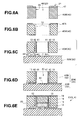
- Figs. 6A to 6E are partial sectional views of a region of one fluorescence sensor 10.
- a large number of elements are collectively formed in a wafer process.
- etching is applied to a conductive (N-type) first silicon wafer 40W via a mask layer 47.
- a large number of frame-like patterns, i.e., the through-hole 46 to be the concave portion 23 is formed.
- Publicly-known various methods can be used for the etching.
- the size of an opening of the through-hole 46 is designed according to specifications. However, since a disposing place is the needle distal end portion 5, for example, an elongated shape having 150 ⁇ m longitudinally and 500 ⁇ m laterally is desirable.
- the side surface 24 of the concave portion 23 is perpendicular to the first principal plane 21.
- the side surface may be a shape having a predetermined angle, i.e., tapered.
- a concave portion having a tapered shape can be manufactured by, for example, wet etching.
- the PD element 13 is formed on the wall surface 45 of the through-hole 46 (the side surface 24 of the concave portion 23). That is, in a state in which the first silicon wafer 40W on which a mask layer 47A is formed is tilted at 5 degrees to 30 degrees, ion implantation processing is performed from four directions. For example, conditions under which boron (B) is introduced are an acceleration voltage of 10 to 100 keV and a dose amount of about 1x10 15 cm -2 . At this point, a thin oxide layer of 50 to 100 nm may be present on the first silicon wafer 40W.
- the silicon oxide layer 42 and the filter 41 are formed in order by a CVD method to cover the PD element 13 on the wall surface 45 of the through-hole 46 of the first silicon wafer 40W. Further, the electrodes 43 and 44 are formed.
- a conductive (N-type) second silicon wafer 30W to be the wiring substrate 30 is separately prepared.
- the wires 61 and 62 for transmitting a detection signal from the PD element 13 and the wires 63 and 64 for supplying a driving signal to the LED element 12 are formed by a sputtering method, a vapor deposition method, or the like.
- the first silicon wafer 40W is vertically reversed and bonded to the second silicon wafer 30W.
- the through-hole 46 of the frame-like substrate 40 is the concave portion 23 having the bottom surface 22.
- the LED element 12 and the transparent resin layer 15 are disposed on an inside of each of a plurality of concave portions 23 of the bonded wafer 20W. Further, the indicator layer 16 is disposed on an upper side of the transparent resin layer 15, when necessary, via a bonding layer such as a silane coupling agent.
- the bonded wafer 20W is singulated and the fluorescence sensor 10 is completed. That is, the needle-type fluorescence sensor 4 including the fluorescence sensor 10 at the needle distal end portion 5 is completed.
- the method of manufacturing a fluorescence sensor is not limited to this.
- a method of, for example, after bonding the singulated wiring substrate 30 and the singulated frame-like substrate 40, disposing the LED element 12 and the like in the concave portion 23 may be used.
- a first silicon wafer may be processed such that an extended portion of the wiring substrate 30 configures the needle main body portion 6 of the needle section 7.
- the needle main body portion 6 and the needle distal end portion 5 including the fluorescence sensor 10, which are separately manufactured, may be bonded to configure the needle section 7.
- the fluorescence sensor 10 according to the present embodiment can be collectively mass-produced by the wafer process. Therefore, the fluorescence sensor 10 can be provided inexpensively and with high quality.
- the LED element 12 causes pulse light emission of the excitation light E having center wavelength of about 375 nm, for example, at an interval of once in thirty seconds.
- a pulse current to the LED element 12 is 1 mA to 100 mA and pulse width of light emission is 10 ms to 100 ms.
- the excitation light E generated by the LED element 12 enter the indicator layer 16 passing through the transparent resin layer 15.
- the indicator layer 16 emits the fluorescent light F of which intensity corresponds to an amount of the analyte 9.
- the analyte 9 penetrates into the indicator layer 16 passing through the light blocking layer 19.
- the fluorescent pigment of the indicator layer 16 generates the fluorescent light F with longer wavelength, for example, wavelength of 460 nm with respect to the excitation light E with wavelength of 375 nm.
- a part of the fluorescent light F generated by the indicator layer 16 enter the PD element 13 through the filter 41 and the silicon oxide layer 42.
- the fluorescent light F is photoelectrically converted in the PD element 13 to generate photogenerated charges to be outputted as a detection signal.
- a part of the excitation light E generated by the LED element 12 enter the side surface 24 of the concave portion 23.
- the excitation light E hardly enter the PD element 13 by the action of the filter 41.
- a computing section (not shown in the figure) of the main body section 2 performs computing processing on the basis of the detection signal, i.e., an electric current due to the photogenerated charges from the PD element 13 or a voltage due to accumulated photogenerated charges and calculates an analyte amount.
- the needle-type fluorescence sensor 4 may include a computing section, a detection signal processing circuit, or the like.
- the fluorescence sensor 10 includes the LED element 12 on the bottom surface 22 of the concave portion 23 of the detection substrate section and includes the PD element 13 on the side surface 24. Therefore, although the fluorescence sensor 10 is very small, detection sensitivity is high.
- a needle-type fluorescence sensor 4A including a fluorescence sensor 10A according to a modification of the first embodiment of the present invention is explained.
- the fluorescence sensor 10A according to this modification is similar to the fluorescence sensor 10 according to the first embodiment. Therefore, the same components are denoted by the same reference numerals and signs and explanation of the components is omitted.
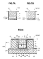
- the LED element 12 of the fluorescence sensor 10 includes a semiconductor 12N of a gallium nitride compound having thickness of about 10 ⁇ m formed on a sapphire substrate 12S having thickness of about 60 to 100 ⁇ m.
- the thickness of the indicator layer 16 of the fluorescence sensor 10 is equal to or smaller than 50 ⁇ m.
- the LED element 12T mainly includes the semiconductor 12N made of the gallium nitride compound. That is, thickness of the LED element 12T is about 10 ⁇ m. Note that a reflection layer 12AA is formed on a side surface of the LED element 12T as well. However, since the thickness of the LED element 12T is small, the reflection layer 12AA may be formed only on a bottom surface of the LED element 12T.
- thickness of the indicator layer 16A can be set to 140 ⁇ m thicker than the indicator layer 16 of the fluorescence sensor 10.
- the fluorescence sensor 10A has the effect of the fluorescence sensor 10. Further, since the indicator layer 16A is thick, the fluorescence sensor 10A can generate a larger amount of the fluorescent light F. Therefore, the fluorescence sensor 10A has higher detection sensitivity.
- the fluorescence sensor 10B according to the present embodiment is similar to the fluorescence sensor 10 according to the first embodiment. Therefore, the same components are denoted by the same reference numerals and signs and explanation of the components is omitted.
- a PD element 13B which is a second photoelectric conversion element, is formed on the bottom surface 22 of the concave portion 23 (an upper surface of a wiring substrate 30B) in addition to a PD element 13A, which is a first photoelectric conversion element, formed on a side surface 24 of the concave portion 23 of a detection substrate section 20B (the wall surface 45 of the through-hole 46 of the frame-like substrate 40).
- a silicon oxide layer 42B which is a third protective layer that protects the PD element 13B, and a filter 41B are disposed to cover the PD element 13B formed on the bottom surface 22.
- the silicon oxide layer 42B has a function same as the function of the silicon oxide layers 42 and 42A.
- the filter 41B has a function same as the function of the filters 41 and 41A.
- a reflection layer 12A1 of the LED element 12 is formed only on the side surface and is not formed on the bottom surface.
- the LED element 12 is a light-emitting element that transmits the fluorescent light F.
- Respective center portions of the PD element 13B, the LED element 12, and the indicator layer 16 are formed in the same region on an upper side of the wiring substrate 30B.
- a large number of PD elements 13B and the respective wires 60 are formed on a surface of a second silicon wafer to be the wiring substrate 30B.
- the filter 41B made of polycrystal silicon or the like is formed on a surface of the silicon oxide layer 42B.
- a detection signal of the PD element 13B is transmitted to the main body section 2 via the wires 65 and 66.
- the PD element 13B In the fluorescence sensor 10B, a part of the fluorescent light F generated by the indicator layer 16 reaches the PD element 13B passing through the LED element 12. Therefore, the PD element 13B generates a detection signal B. That is, the LED element 12 not including a reflection layer on the bottom surface transmits the fluorescent light F.
- the fluorescence sensor 10B outputs, to the main body section 2, not only the detection signal A outputted by the PD element 13A but also the detection signal B outputted by the PD element 13B.
- the fluorescence sensor 10B has the effect of the fluorescence sensor 10 and has higher detection sensitivity.
- a reflection layer may be formed on the bottom surface of the LED element 12 either.
- the part of the fluorescent light F does not enter the PD element 13B.
- a noise light component of a detection signal of the PD element 13B due to the excitation light E from the LED element 12 can be further reduced.
- the PD element 13B does not have to be formed in a region opposed to the bottom surface of the LED element 12 in order to reduce the noise light component. That is, the PD element 13B only has to be formed in at least a part of the bottom surface 22 of the concave portion 23.
- a thinned LED element same as the LED element 12T in the modification of the first embodiment may be used.
- a needle-type fluorescence sensor 4C including a fluorescence sensor 10C according to a modification of the second embodiment of the present invention is explained. Since the fluorescence sensor 10C according to this modification is similar to the fluorescence sensor 10B according to the second embodiment, the same components are denoted by the same reference numerals and signs and explanation of the components is omitted.
- the fluorescence sensor 10B outputs, to the main body section 2 respectively via the different wires 61, 62, 65, and 66, the detection signal A outputted by the PD element 13A and the detection signal B outputted by the PD element 13B.
- the fluorescence sensor C outputs, to the main body section 2 using the two wires 67 and 68, an aggregated detection signal of the detection signal A outputted by the PD element 13A and the detection signal B outputted by the PD element 13B.
- a part of the PD element 13B formed on a wiring substrate 30C is extended to right under the frame-like substrate 40 and connected to the wire 68 of the PD element 13A right under the wire 68.
- a low-resistance region 30H of the wiring substrate 30C formed by a method same as the method of forming the low-resistance region 40H is connected to the common wire 67 right under the low-resistance region 40H of the frame-like substrate 40.
- Electrical connection is performed using, for example, a flip-chip mounting technique or a solder connection technique.
- the fluorescence sensor 10C has an effect of the fluorescence sensor 10B and the like. Further, since the number of the wires 60 for outputting a detection signal is as small as two, the fluorescence sensor 10C is smaller.
- a needle-type fluorescence sensor 4D including a fluorescence sensor 10D according to a modification of a third embodiment of the present invention is explained.
- the fluorescence sensor 10D according to this modification is similar to the fluorescence sensor 10 according to the first embodiment and the like, the same components are denoted by the same reference numerals and signs and explanation of the components is omitted.
- a detection substrate section 20D of the fluorescence sensor 10D is integrally manufactured by a silicon wafer 20DW, which is a semiconductor substrate. That is, a concave portion 23D of the detection substrate section 20D is a concave portion formed on the first principal plane 21 of the silicon wafer 20DW by, for example, an etching method.
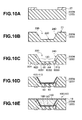
- Figs. 10A to 10E are partial sectional views of a region of one fluorescence sensor 10D.
- a large number of elements are collectively formed in a wafer process.
- a mask layer 27 is manufactured on the first principal plane 21 of the silicon wafer 20DW.
- the concave portion 23D having a bottom surface 22D parallel to the first principal plane 21 is formed by the etching method.
- etching method a wet etching method in which a tetramethylammonium hydroxide (TMAH) solution, a potassium hydroxide (KOH) water solution, or the like is used is desirable.
- TMAH tetramethylammonium hydroxide
- KOH potassium hydroxide
- a dry etching method such as reactive ion etching (RIE), chemical dry etching (CDE), or the like can also be used.
- a side surface 24D of the concave portion 23D is the (111) surface and an angle ⁇ 1 between the (111) surface and the (100) surface is 54.74 degrees. That is, an opening of the concave portion 23D is wider than the bottom surface.
- the side surface 24D is formed in a tapered shape.
- a PD element 13D is formed on the side surface 24D of the concave portion 23D.
- the concave portion 23D having the tapered side surface 24D has a large area in which the PD element is formed compared with the concave portion 23 having the vertical side surface 24. Moreover, it is easy to form the PD element 13D on the side surface 24D of the concave portion 23D.
- wires 63 and 64 for a driving signal of a LED element 12D, wires 61D and 62D for a detection signal of the PD element 13D, and the like are formed.
- through-wires 60S 1, 60S2, and 60S3 for the LED element 12D and the PD element 13D may be manufactured before the formation of the PD element 13D.
- a low-resistance region 20H is formed by a method same as the method of forming the low-resistance region 40H.
- a silicon oxide layer 42D and a filter 41D are disposed to cover the PD element 13D on the side surface 24D.
- the silicon oxide layer 42D has a configuration and a function same as the configuration and the function of the silicon oxide layer 42.
- the filter 41D has a configuration and a function same as the configuration and the function of the filter 41.
- the LED element 12D including a reflection layer 12AD is disposed on the bottom surface 22D of the concave portion 23D. Further, an indicator layer 16D is disposed via a transparent resin layer 15D. Further, the silicon wafer 20DW on which a light blocking layer 19D is formed is singulated, whereby the fluorescence sensor 10D is completed.
- a side surface of a concave portion may be perpendicular to the first principal plane 21.
- the LED element 12D of the fluorescence sensor 10D according to the third embodiment is a thinned LED element same as the LED element 12T according to the modification of the first embodiment.
- the fluorescence sensor 10D has an effect of the fluorescence sensor 10 and the like. Further, the fluorescence sensor 10D is easily manufactured and has higher sensitivity.
- a needle-type fluorescence sensor 4E including a fluorescence sensor 10E according to a modification of the third embodiment of the present invention is explained.
- the fluorescence sensor 10E according to this modification is similar to the fluorescence sensor 10D according to the third embodiment and the like. Therefore, the same components are denoted by the same reference numerals and signs and explanation of the components is omitted.
- a PD element 13E which is a photoelectric conversion element, is formed on the side surface 24D of the concave portion 23D of the detection substrate section 20D and the bottom surface 22D of the concave portion 23D.
- the PD element 13E is formed simultaneously on the side surface 24D and the bottom surface 22D of the concave portion 23D of a silicon wafer 20EW on which the concave portion 23D having the bottom surface 22D parallel to the first principal plane 21 is formed. That is, a PD element formed on the side surface 24D and a PD element formed on the bottom surface are the integral PD element 13E.
- a silicon oxide layer 42E to be a first protective film of the PD element 13E is formed.
- a filter 41E made of polycrystal silicon or the like is formed on a surface of the silicon oxide layer 42E.
- an LED element 12E does not include a reflection layer on a bottom surface.
- the PD element 13E detects the fluorescent light F transmitted through the LED element 12E as well. Therefore, detection sensitivity is high.
- the PD element 13E integrally formed on the side surface 24D and the bottom surface 22D is easily formed.
- wires for a detection signal only have to be two wires 61E and 62E.
- the silicon oxide layer 42E and the filter 41E can also be integrally formed on the side surface 24D and the bottom surface 22D.
- the PD element 13D may be divided into a plurality of regions. Detection signals of the respective regions may be transmitted to the main body section 2 by separate wires.
- the fluorescence sensor 10E has the effect of the fluorescence sensor 10D. Further, the fluorescence sensor 10E has high sensitivity and is easily manufactured.
- a needle-type fluorescence sensor 4F (4F1, 4F2) including a fluorescence sensor 10F (10F1, 10F2) according to a fourth embodiment of the present invention is explained.
- the fluorescence sensor 10F according to the present embodiment is similar to the fluorescence sensor 10 according to the first embodiment and the like. Therefore, the same components are denoted by the same reference numerals and signs and explanation of the components is omitted.
- the fluorescence sensor 10F includes a long-wavelength cut filter 51 configured to cut long-wavelength light including excitation light having high transmittance in a wavelength range of the fluorescent light F and having low transmittance in a wavelength range longer than the wavelength range of the fluorescent light F among lights generated by the LED element 12.
- the LED element 12 generates the excitation light E having center frequency of, for example, about 375 nm.
- the excitation light E sometimes includes a slight amount of light having wavelength longer than the wavelength of the fluorescent light F. That is, because of an influence of a crystal defect inherent in a crystal forming the LED element 12, in some case, faint emitted light appears from the LED element 12 in a wavelength range wide on a long wavelength side. Further, reception sensitivity of the PD element 13 is high on the long wavelength side. Transmittance of the filter is also high on the long wavelength side.
- a wavelength component spectrum longer than the wavelength of the fluorescent light F of the LED element 12 does not contribute to fluorescent light generation of the indicator layer 16. Moreover, even if the wavelength component spectrum is weak, the wavelength component spectrum is a significant cause of a noise component of a detection signal.
- a transmittance characteristic of a long-wavelength cut filter 51 suitable for detection of the florescent light F with peak wavelength of 475 nm, a short wavelength end of 425 nm, and a long wavelength end of 650 nm is shown.
- the long-wavelength cut filter 51 is transparent in a wavelength range of the fluorescent light F.
- the long-wavelength cut filter 51 is a dielectric multilayer film manufactured by laminating multiple layers of dielectrics such as LaF 3 , Al 2 O 3 , Pr 2 O 3 , Ta 2 O 3 , TiO 2 , or Nb 2 O 5 .
- a long-wavelength cut filter 51A is disposed above the LED element 12F1 including a reflection layer 12F1A.
- long-wavelength cut filters 51B1 and 51B2 are dispose above and below the LED element 12.
- a method of forming a long-wavelength cut filter is not limited to a method including inserting a solid-state filter such as a dielectric multilayer film.
- the long-wavelength filter may be formed by a method including applying and solidifying fluid-state resin or a method including, for example, depositing the resin on both surfaces of the LED element 12.
- the fluorescence sensor 10F since long-wavelength light generated by the LED element 12 is cut by the long-wavelength cut filter 51, noise light to be an offset output is removed. Therefore, S/N of a detection signal is improved. Consequently, the fluorescence sensor 10F has the effect of the fluorescence sensor 10 or the like and has higher sensitivity.
Landscapes
- Health & Medical Sciences (AREA)
- Life Sciences & Earth Sciences (AREA)
- Physics & Mathematics (AREA)
- Engineering & Computer Science (AREA)
- General Health & Medical Sciences (AREA)
- Pathology (AREA)
- Animal Behavior & Ethology (AREA)
- Biomedical Technology (AREA)
- Public Health (AREA)
- Surgery (AREA)
- Medical Informatics (AREA)
- Molecular Biology (AREA)
- Heart & Thoracic Surgery (AREA)
- Biophysics (AREA)
- Veterinary Medicine (AREA)
- Chemical & Material Sciences (AREA)
- Optics & Photonics (AREA)
- General Physics & Mathematics (AREA)
- Immunology (AREA)
- Biochemistry (AREA)
- Analytical Chemistry (AREA)
- Chemical Kinetics & Catalysis (AREA)
- Plasma & Fusion (AREA)
- Computer Vision & Pattern Recognition (AREA)
- Spectroscopy & Molecular Physics (AREA)
- Physiology (AREA)
- Psychiatry (AREA)
- Signal Processing (AREA)
- Emergency Medicine (AREA)
- Artificial Intelligence (AREA)
- Nuclear Medicine, Radiotherapy & Molecular Imaging (AREA)
- Investigating, Analyzing Materials By Fluorescence Or Luminescence (AREA)
- Investigating Or Analysing Materials By The Use Of Chemical Reactions (AREA)
Abstract
Description
- The present invention relates to a fluorescence sensor for measuring a concentration of an analyte and, more particularly, to a fluorescence sensor, which is a micro-fluorescence spectrophotometer, manufactured using a semiconductor manufacturing technique and an MEMS technique.
- Various analyzers for checking presence of an analyte, i.e., a substance to be measured in liquid or measuring a concentration of the analyte have been developed. For example, there is a known fluorescence spectrophotometer for injecting a fluorescent pigment, which changes in characteristics because of the presence of an analyte and generates fluorescent light, and a solution to be measured including the analyte into a transparent container having a fixed capacity and irradiating an excitation light E to measure fluorescent light intensity from the fluorescent pigment to thereby measure the concentration of the analyte.
- A small fluorescence spectrophotometer includes a photodetector and an indicator layer containing a fluorescent pigment. When the excitation light E from a light source is irradiated on the indicator layer into which the analyte in the solution to be measured can penetrate, the fluorescent pigment in the indicator layer generates fluorescent light with a light amount corresponding to the analyte concentration in the solution to be measured. The photodetector receives the fluorescent light. The photodetector is a photoelectric conversion element. The photodetector outputs an electric signal corresponding to the light amount of the received fluorescent light. The analyte concentration in the solution to be measured is measured from the electric signal.
- In recent years, in order to measure an analyte in a micro-volume sample, a micro-fluorescence spectrophotometer manufactured using the semiconductor manufacturing technique and the MEMS technique has been proposed. The micro-fluorescence spectrophotometer is hereinafter referred to as "fluorescence sensor".
- For example, a
fluorescence sensor 110 shown inFigs. 1 and 2 is disclosed in United States Patent No.5039490 . Thefluorescence sensor 110 is configured by a transparent supportingsubstrate 101 through which excitation E can be transmitted, an opticaltabular section 105 including a photoelectricconversion element section 103 configured to convert fluorescent light into an electric signal and a light-condensing function section 105A configured to condense the excitation light E, anindicator layer 106 configured to interact with ananalyte 9 to thereby generate fluorescent light through incidence of the excitation light E, and acover layer 109. - The photoelectric
conversion element section 103 is, for example, a photoelectric conversion element formed on asubstrate 103A made of silicon. Thesubstrate 103A does not transmit the excitation light E. Therefore, thefluorescence sensor 110 includes, around the photoelectricconversion element section 103, anair gap region 120 through which the excitation light E can be transmitted. - That is, only the excitation light E transmitted through the
air gap region 120 and entered the opticaltabular section 105 is condensed to the vicinity of an upper part of the photoelectricconversion element section 103 in theindicator layer 106 by the action of the opticaltabular section 105. Fluorescent light F is generated by interaction of condensed excitation light E2 and theanalyte 9 penetrating into an inside of theindicator layer 106. A part of the generated fluorescent light F enters the photoelectricconversion element section 103. A signal of an electric current, a voltage, or the like proportional to fluorescent light intensity, i.e., the concentration of theanalyte 9 is generated in the photoelectricconversion element section 103. Note that the excitation light E does not enter the photoelectricconversion element section 103 by the action of a filter (not shown in the figure) that covers the photoelectricconversion element section 103. - As explained above, in the
fluorescence sensor 110, on the transparent supportingsubstrate 101, a photodiode which is the photoelectricconversion element section 103 is formed on thesubstrate 103A in which theair gap region 120, which is a passage of the excitation light E, is secured. The opticaltabular section 105 and theindicator layer 106 are laminated on an upper side of thesubstrate 103A. - However, the publicly-known
fluorescence sensor 110 includes theair gap region 120, which is the passage of the excitation light E, and the region of the photoelectricconversion element section 103 on the same plane. Therefore, the area of theair gap region 120, which is the passage, is increased in order to guide a larger amount of the excitation light E to theindicator layer 106, since the area of the photoelectricconversion element section 103 decreases, the sensitivity of the fluorescence sensor is not increased. Conversely, when the area of the photoelectricconversion element section 103 is increased in order to increase the detection sensitivity of the photoelectricconversion element section 103, the area of theair gap region 120, which is the passage of the excitation light E, decreases and the excitation light E guided to theindicator layer 106 decreases. Therefore, similarly, the sensitivity of the fluorescence sensor is not increased. That is, in thefluorescence sensor 110, it is not easy to obtain high detection sensitivity. - It is an object of an embodiment of the present invention to provide a fluorescence sensor having high detection sensitivity.
- A fluorescence sensor according to an aspect of the present invention includes: a detection substrate section, on a first principal plane of which a concave portion having a bottom surface parallel to the first principal plane is present and, in at least a part of a side surface of the concave portion of which a photoelectric conversion element configured to receive fluorescent light and output a detection signal is formed; a light-emitting element disposed on the bottom surface of the concave portion of the detection substrate section and configured to generate excitation light; and an indicator layer disposed on an inside of the concave portion on an upper side of the light-emitting element and configured to generate the fluorescent light corresponding to the excitation light and an analyte amount.
-
-
Fig. 1 is an explanatory diagram showing a sectional structure of a publicly-known fluorescence sensor; -
Fig. 2 is an exploded view for explaining the structure of the publicly-known fluorescence sensor; -
Fig. 3 is an explanatory diagram for explaining a sensor system including a fluorescence sensor according to a first embodiment; -
Fig. 4 is an exploded view for explaining the structure of the fluorescence sensor according to the first embodiment; -
Fig. 5 is a schematic diagram showing a sectional structure of the fluorescence sensor according to the first embodiment; -
Fig. 6A is a schematic diagram showing a sectional structure for explaining a method of manufacturing a fluorescence sensor according to the first embodiment; -
Fig. 6B is a schematic diagram showing a sectional structure for explaining the method of manufacturing a fluorescence sensor according to the first embodiment; -
Fig. 6C is a schematic diagram showing a sectional structure for explaining the method of manufacturing a fluorescence sensor according to the first embodiment; -
Fig. 6D is a schematic diagram showing a sectional structure for explaining the method of manufacturing a fluorescence sensor according to the first embodiment; -
Fig. 6E is a schematic diagram showing a sectional structure for explaining the method of manufacturing a fluorescence sensor according to the first embodiment; -
Fig. 7A is a schematic diagram showing a sectional structure of the fluorescence sensor according to the first embodiment; -
Fig. 7B is a schematic diagram showing a sectional structure of a fluorescence sensor according to a modification of the first embodiment; -
Fig. 8 is a schematic diagram showing a sectional structure of a fluorescence sensor according to a second embodiment; -
Fig. 9 is a schematic diagram showing a sectional structure of a fluorescence sensor according to a modification of the second embodiment; -
Fig. 10A is a schematic diagram showing a sectional structure for explaining a method of manufacturing a fluorescence sensor according to a third embodiment; -
Fig. 10B is a schematic diagram showing a sectional structure for explaining the method of manufacturing a fluorescence sensor according to the third embodiment; -
Fig. 10C is a schematic diagram showing a sectional structure for explaining the method of manufacturing a fluorescence sensor according to the third embodiment; -
Fig. 10D is a schematic diagram showing a sectional structure for explaining the method of manufacturing a fluorescence sensor according to the third embodiment; -
Fig. 10E is a schematic diagram showing a sectional structure for explaining the method of manufacturing a fluorescence sensor according to the third embodiment; -
Fig. 11 is a schematic diagram showing a sectional structure of a fluorescence sensor according to a fourth embodiment; -
Fig. 12 is a diagram showing a characteristic of a long wavelength cut filter of a fluorescence sensor according to a fifth embodiment; -
Fig. 13A is a schematic diagram showing a sectional structure of the fluorescence sensor according to the fifth embodiment; and -
Fig. 13B is a schematic diagram showing a sectional structure of the fluorescence sensor according to the fifth embodiment. - A
fluorescence sensor 10 according to a first embodiment of the present invention is explained below. - As shown in
Fig. 3 , a needle-type fluorescence sensor 4 including thefluorescence sensor 10 configures a sensor system 1 in conjunction with amain body section 2 and areceiver 3. - That is, the sensor system 1 includes the needle-
type fluorescence sensor 4, themain body section 2, and thereceiver 3 that receives and stores a signal from themain body section 2. Transmission and reception of a signal between themain body section 2 and thereceiver 3 is performed by radio or by wire. - The needle-
type fluorescence sensor 4 includes aneedle section 7 including a needledistal end portion 5, which includes thefluorescence sensor 10 as a main functional section, and an elongated needlemain body portion 6, and aconnector section 8 integrated with a rear end portion of the needlemain body portion 6. The needledistal end portion 5, the needlemain body portion 6, and theconnector section 8 may be integrally formed by the same material. - The
connector section 8 detachably fits with afitting section 2A of themain body section 2. Theconnector section 8 mechanically fits with thefitting section 2A of themain body section 2, whereby a plurality ofwires 60 extended from thefluorescence sensor 10 of the needle-type fluorescence sensor 4 are electrically connected to themain body section 2. In the following explanation, the plurality ofwires 60 are respectively indicated by wires 61 (to 68). - Although not shown in the figure, the
main body section 2 includes a computing section configured to process a detection signal from thefluorescence sensor 10, a radio antenna for transmitting and receiving a radio signal between themain body section 2 and thereceiver 3, and a battery and the like. When wired transmission and reception is performed between themain body section 2 and thereceiver 3, themain body section 2 includes a signal line instead of the radio antenna. - The
fluorescence sensor 10 is a disposable section that is discarded after use to prevent infection. However, themain body section 2 and thereceiver 3 are reusable sections that are repeatedly reused. Note that, when themain body section 2 includes a memory section having enough capacity, thereceiver 3 is unnecessary. - In a state in which the needle-
type fluorescence sensor 4 is fit with themain body section 2, a subject himself/herself stabs the needle-type fluorescence sensor 4 from the body surface. The needledistal end portion 5 is retained in the body. For example, the needle-type fluorescence sensor 4 continuously measures glucose concentration in body fluid and stores the glucose concentration in a memory of thereceiver 3. That is, thefluorescence sensor 10 according to the present embodiment is a sensor of a short-term subcutaneous retaining type that is continuously used for about one week. - As shown in
Fig. 4 and 5 , thefluorescence sensor 10, which is a main functional section of the needle-type fluorescence sensor 4, includes adetection substrate section 20, a light emitting diode (hereinafter also referred to as "LED")element 12, which is a light-emitting element that generates the excitation light E, atransparent resin layer 15, anindicator layer 16 that generates the fluorescent light F corresponding to the excitation light E and an analyte amount, and alight blocking layer 19. - The
detection substrate section 20 is manufactured by bonding awiring substrate 30 and a frame-like substrate 40 in which a through-hole 46 is formed. Therefore, in thedetection substrate section 20, on a firstprincipal plane 21, aconcave portion 23 having abottom surface 22 parallel to the firstprincipal plane 21 is present. That is, a surface of thewiring substrate 30 is thebottom surface 22 of theconcave portion 23. Awall surface 45 of the through-hole 46 of the frame-like substrate 40 is aside surface 24 of theconcave portion 23. Note that insulation layers are formed as appropriate on, for example, surfaces of thedetection substrate section 20 made of an N-type semiconductor, i.e., thewiring substrate 30 and the frame-like substrate 40. However, the insulation layers are not shown in the figures. - The
LED element 12 is disposed on thebottom surface 22 of theconcave portion 23. Theindicator layer 16 is disposed on an upper side of theLED element 12 on an inside of theconcave portion 23. Note that, for example, areflection layer 12A made of metal with high reflectivity is formed on a bottom surface and a side surface of theLED element 12. TheLED element 12 generates the excitation light E only toward theindicator layer 16. TheLED element 12 having thereflection layer 12A on the bottom surface irradiates the excitation light E, which has a light amount about twice as large as a light amount of an LED element without a reflection layer, toward theindicator layer 16. Irradiation of noise light due to the excitation light E on theindicator layer 16 can be prevented by thereflection layer 12A on the side surface. The same effect can be obtained when, instead of thereflection layer 12A, aPD element 13 is formed in a region of theside surface 24 of theconcave portion 23 opposed to the side surface of theLED element 12. - The light-emitting element is not limited to the
LED element 12 and is selected out of various kinds of light-emitting elements such as an organic EL element, an inorganic EL element, and a laser diode element. TheLED element 12 is desirable from the viewpoints of, for example, fluorescent light transmittance, light generation efficiency, and broadness of wavelength selectivity of the excitation light E and that only a little light having wavelength other than an ultraviolet ray, which is the excitation light E, is generated. - The
transparent resin layer 15 is a second protective layer. As the second protective layer, epoxy resin, silicone resin, transparent amorphous fluorocarbon resin, or the like can be used. The second protective layer is selected out of materials having characteristics that, for example, the materials have electric insulation, have moisture barrier properties, and have satisfactory transparency to the excitation light E and the fluorescent light F. - As the characteristics of the second protective layer, it is important that generation of the fluorescent light F in the layer is small even if the excitation light E is irradiated. It goes without saying that the characteristic that the fluorescent light F is small is an important characteristic of all transparent materials of the
fluorescence sensor 10 excluding theindicator layer 16. - The
indicator layer 16 generates, with the interaction with ananalyte 9 penetrating into theindicator layer 16 and the excitation light E, the fluorescent light F having a light amount corresponding to the concentration of ananalyte 9. Thickness of theindicator layer 16 is set to several tens of micrometers to about 200 µm. Theindicator layer 16 is configured by a base material including a fluorescent pigment that generates the fluorescent light F having intensity corresponding to an amount of theanalyte 9, i.e., analyte concentration in a specimen. - The fluorescent pigment is selected according to a type of the
analyte 9. Any fluorescent pigment can be used as long as the light amount of the generated fluorescent light F reversibly changes according to the amount of theanalyte 9. For example, when hydrogen ion concentration or carbon dioxide in a living organism is measured, a hydroxypyrene-tri sulfonic acid derivative, a phenylboronic acid derivative having a fluorescence residue when saccharides are measured, a crown ether derivative having a fluorescence residue when a potassium ion is measured, or the like can be used. When saccharides such as glucose are measured, as the fluorescent pigment, a ruthenium organic complex, a fluorescence phenylboronic acid derivative, or a substance reversibly coupled to glucose such as fluorescein coupled to protein can be used. - As explained above, the
fluorescence sensor 10 according to the present invention is adapted to various uses such as an oxygen sensor, a glucose sensor, a pH sensor, an immunosensor, and a microbial sensor according to the selection of the fluorescent pigment. - The
indicator layer 16 has, for example, an easily-hydrated hydrogel as a base material. In the hydrogel, the fluorescent pigment is contained or coupled. As a component of the hydrogel, a polysaccharide such as methylcellulose or dextran, acrylic hydrogel manufactured by polymerizing monomer such as (meta)acrylamide, methylol acrylamide, or hydroxyethyl acrylate, urethane hydrogel manufactured from polyethylene glycol and diisocyanate, or the like can be used. - The
indicator layer 16 is bonded on thetransparent resin layer 15 via a not-shown adhesive layer formed of a silane coupling agent or the like. Note that a structure in which thetransparent resin layer 15 is not formed and theindicator layer 16 is directly bonded to the surface of theLED element 12 may be adopted. - The
light blocking layer 19 is a layer having thickness equal to or smaller than several tens of micrometers formed on an upper surface side of theindicator layer 16. Thelight blocking layer 19 prevents the excitation light E and the fluorescent light F from leaking to an outside of thefluorescence sensor 10 and, at the same time, prevents external light from penetrating into theconcave portion 23. - On the other hand, the photodiode (hereinafter also referred to as "PD")
element 13, which is a photoelectric conversion element that receives the fluorescent light F and outputs a detection signal, is formed on thewall surface 45 of the through-hole 46 of the frame-like substrate 40, i.e., theside surface 24 of theconcave portion 23 of thedetection substrate section 20. That is, thePD element 13 is provided to surround theindicator layer 16 and formed such that a light receiving surface faces theindicator layer 16. - The
PD element 13 may be formed over theentire side surface 24. However, in order to efficiently receive only the fluorescent light F, thePD element 13 may be formed only in an opposed region of theindicator layer 16. Theindicator layer 16 may be formed on all four surfaces of theside surface 24 or may be formed in on a part of the four surfaces. - That is, the
PD element 13 only has to be formed in at least a part of theside surface 24 of theconcave portion 23. - As the photoelectric conversion element, a photoconductor, a phototransistor (PT), or the like may be used.
- A
silicon oxide layer 42, which is a first protective layer that protects thePD element 13, and afilter 41 are disposed to cover thePD element 13 formed on theside surface 24. Thefilter 41 is formed on a light-receiving surface side of thePD element 13 to cover thePD element 13. - The
filter 41 is, for example, an absorption type filter that cuts the excitation light E without allowing the excitation light E to pass and allows the fluorescent light F having wavelength longer than the wavelength of the excitation light E to pass. As a material of such a filter, a silicon layer or a silicon carbide layer is suitable. Thefilter 41 may be a band-pass filter that allows only the fluorescent light F to pass. - The frame-
like substrate 40 includes twowires electrodes PD element 13 to themain body section 2 and twowires electrode 12B of the LED element. An N-type impurity, for example, phosphorus or arsenic is partially introduced to a surface of the frame-like substrate 40, which is an N-type semiconductor to form a low-resistance region 40H having higher electric conductivity. Theelectrode 44 is formed on the low-resistance region 40H. - The material of the frame-
like substrate 40 is desirably monocrystal silicon in order to form thePD element 13 on the frame-like substrate 40. However, the material may be glass, ceramic, or the like. - It is desirable to prevent the fluorescent light F generated by the
indicator layer 16 from leaking to an outside and block the external light to prevent the external light from penetrating into theconcave portion 23. That is, it is desirable to coat, with a material same as thelight blocking layer 19 or resin mixed with carbon black, the outer wall and the secondprincipal plane 25 of thedetection substrate section 20 or deposit a metal layer on the outer wall and the secondprincipal plane 25. - The excitation light E generated by the
LED element 12 is irradiated on the fluorescent pigment in theindicator layer 16. A part of the fluorescent light F generated by the fluorescent pigment through the interaction with theanalyte 9 reaches thePD element 13 passing through thefilter 41 and is converted into a detection signal. - The
fluorescence sensor 10 has high detection sensitivity because thefluorescence sensor 10 detects the fluorescent light F with thePD element 13 formed on theside surface 24 that surrounds theindicator layer 16. - Next, a method of manufacturing the
fluorescence sensor 10 is briefly explained.Figs. 6A to 6E are partial sectional views of a region of onefluorescence sensor 10. However, in an actual process, a large number of elements are collectively formed in a wafer process. - First, as shown in
Fig. 6A , in manufacturing of the frame-like substrate 40, etching is applied to a conductive (N-type)first silicon wafer 40W via amask layer 47. A large number of frame-like patterns, i.e., the through-hole 46 to be theconcave portion 23 is formed. Publicly-known various methods can be used for the etching. - The size of an opening of the through-
hole 46 is designed according to specifications. However, since a disposing place is the needledistal end portion 5, for example, an elongated shape having 150 µm longitudinally and 500 µm laterally is desirable. - In the
fluorescence sensor 10, theside surface 24 of theconcave portion 23 is perpendicular to the firstprincipal plane 21. However, as explained below, the side surface may be a shape having a predetermined angle, i.e., tapered. A concave portion having a tapered shape can be manufactured by, for example, wet etching. - Subsequently, as shown in
Fig. 6B , thePD element 13 is formed on thewall surface 45 of the through-hole 46 (theside surface 24 of the concave portion 23). That is, in a state in which thefirst silicon wafer 40W on which amask layer 47A is formed is tilted at 5 degrees to 30 degrees, ion implantation processing is performed from four directions. For example, conditions under which boron (B) is introduced are an acceleration voltage of 10 to 100 keV and a dose amount of about 1x1015 cm-2. At this point, a thin oxide layer of 50 to 100 nm may be present on thefirst silicon wafer 40W. - The
silicon oxide layer 42 and thefilter 41 are formed in order by a CVD method to cover thePD element 13 on thewall surface 45 of the through-hole 46 of thefirst silicon wafer 40W. Further, theelectrodes - A conductive (N-type)
second silicon wafer 30W to be thewiring substrate 30 is separately prepared. On thesecond silicon wafer 30W, thewires PD element 13 and thewires LED element 12 are formed by a sputtering method, a vapor deposition method, or the like. - As shown in
Fig. 6C , thefirst silicon wafer 40W is vertically reversed and bonded to thesecond silicon wafer 30W. - Then, as shown in
Fig. 6D , in a bondedwafer 20W in which the two wafers are bonded, the through-hole 46 of the frame-like substrate 40 is theconcave portion 23 having thebottom surface 22. - As shown in
Fig. 6E , on an inside of each of a plurality ofconcave portions 23 of the bondedwafer 20W, theLED element 12 and thetransparent resin layer 15 are disposed. Further, theindicator layer 16 is disposed on an upper side of thetransparent resin layer 15, when necessary, via a bonding layer such as a silane coupling agent. - For the disposing of the
LED element 12, methods including various bonding methods such as a bonding method in which optically transparent acrylic resin, silicon resin, or the like is used and a flip-chip bonding method can be used. - Finally, after the
light blocking layer 19 is formed to cover theindicator layer 16, the bondedwafer 20W is singulated and thefluorescence sensor 10 is completed. That is, the needle-type fluorescence sensor 4 including thefluorescence sensor 10 at the needledistal end portion 5 is completed. - The method of manufacturing a fluorescence sensor is not limited to this. A method of, for example, after bonding the
singulated wiring substrate 30 and the singulated frame-like substrate 40, disposing theLED element 12 and the like in theconcave portion 23 may be used. - A first silicon wafer may be processed such that an extended portion of the
wiring substrate 30 configures the needlemain body portion 6 of theneedle section 7. The needlemain body portion 6 and the needledistal end portion 5 including thefluorescence sensor 10, which are separately manufactured, may be bonded to configure theneedle section 7. - As explained above, the
fluorescence sensor 10 according to the present embodiment can be collectively mass-produced by the wafer process. Therefore, thefluorescence sensor 10 can be provided inexpensively and with high quality. - Next, the operation of the
fluorescence sensor 10 is explained with reference toFig. 5 . - The
LED element 12 causes pulse light emission of the excitation light E having center wavelength of about 375 nm, for example, at an interval of once in thirty seconds. For example, a pulse current to theLED element 12 is 1 mA to 100 mA and pulse width of light emission is 10 ms to 100 ms. - The excitation light E generated by the
LED element 12 enter theindicator layer 16 passing through thetransparent resin layer 15. Theindicator layer 16 emits the fluorescent light F of which intensity corresponds to an amount of theanalyte 9. Theanalyte 9 penetrates into theindicator layer 16 passing through thelight blocking layer 19. The fluorescent pigment of theindicator layer 16 generates the fluorescent light F with longer wavelength, for example, wavelength of 460 nm with respect to the excitation light E with wavelength of 375 nm. - A part of the fluorescent light F generated by the
indicator layer 16 enter thePD element 13 through thefilter 41 and thesilicon oxide layer 42. The fluorescent light F is photoelectrically converted in thePD element 13 to generate photogenerated charges to be outputted as a detection signal. Note that a part of the excitation light E generated by theLED element 12 enter theside surface 24 of theconcave portion 23. However, the excitation light E hardly enter thePD element 13 by the action of thefilter 41. - In the
fluorescence sensor 10, a computing section (not shown in the figure) of themain body section 2 performs computing processing on the basis of the detection signal, i.e., an electric current due to the photogenerated charges from thePD element 13 or a voltage due to accumulated photogenerated charges and calculates an analyte amount. Note that the needle-type fluorescence sensor 4 may include a computing section, a detection signal processing circuit, or the like. - The
fluorescence sensor 10 includes theLED element 12 on thebottom surface 22 of theconcave portion 23 of the detection substrate section and includes thePD element 13 on theside surface 24. Therefore, although thefluorescence sensor 10 is very small, detection sensitivity is high. - Next, a needle-
type fluorescence sensor 4A including afluorescence sensor 10A according to a modification of the first embodiment of the present invention is explained. Thefluorescence sensor 10A according to this modification is similar to thefluorescence sensor 10 according to the first embodiment. Therefore, the same components are denoted by the same reference numerals and signs and explanation of the components is omitted. - As shown in
Fig. 7A , theLED element 12 of thefluorescence sensor 10 according to the first embodiment includes asemiconductor 12N of a gallium nitride compound having thickness of about 10 µm formed on a sapphire substrate 12S having thickness of about 60 to 100 µm. - Therefore, for example, when thickness of the
LED element 12 is 100 µm and depth of the concave portion is 150 µm, the thickness of theindicator layer 16 of thefluorescence sensor 10 is equal to or smaller than 50 µm. - On the other hand, as shown in
Fig. 7B , in anLED element 12T of thefluorescence sensor 10A, most of the sapphire substrate 12S is removed from theLED element 12. TheLED element 12T mainly includes thesemiconductor 12N made of the gallium nitride compound. That is, thickness of theLED element 12T is about 10 µm. Note that a reflection layer 12AA is formed on a side surface of theLED element 12T as well. However, since the thickness of theLED element 12T is small, the reflection layer 12AA may be formed only on a bottom surface of theLED element 12T. - In the
fluorescence sensor 10A, for example, when the depth of the concave portion is 150 µm, thickness of theindicator layer 16A can be set to 140 µm thicker than theindicator layer 16 of thefluorescence sensor 10. - The
fluorescence sensor 10A has the effect of thefluorescence sensor 10. Further, since theindicator layer 16A is thick, thefluorescence sensor 10A can generate a larger amount of the fluorescent light F. Therefore, thefluorescence sensor 10A has higher detection sensitivity. - Next, a needle-
type fluorescence sensor 4B including afluorescence sensor 10B according to a second embodiment of the present invention is explained. Thefluorescence sensor 10B according to the present embodiment is similar to thefluorescence sensor 10 according to the first embodiment. Therefore, the same components are denoted by the same reference numerals and signs and explanation of the components is omitted. - As shown in
Fig. 8 , in thefluorescence sensor 10B, aPD element 13B, which is a second photoelectric conversion element, is formed on thebottom surface 22 of the concave portion 23 (an upper surface of awiring substrate 30B) in addition to aPD element 13A, which is a first photoelectric conversion element, formed on aside surface 24 of theconcave portion 23 of adetection substrate section 20B (thewall surface 45 of the through-hole 46 of the frame-like substrate 40). - A
silicon oxide layer 42B, which is a third protective layer that protects thePD element 13B, and afilter 41B are disposed to cover thePD element 13B formed on thebottom surface 22. Thesilicon oxide layer 42B has a function same as the function of the silicon oxide layers 42 and 42A. Thefilter 41B has a function same as the function of thefilters LED element 12 is formed only on the side surface and is not formed on the bottom surface. TheLED element 12 is a light-emitting element that transmits the fluorescent light F. - Respective center portions of the
PD element 13B, theLED element 12, and theindicator layer 16 are formed in the same region on an upper side of thewiring substrate 30B. - In a manufacturing process for the
fluorescence sensor 10B, a large number ofPD elements 13B and the respective wires 60 (61 to 66) are formed on a surface of a second silicon wafer to be thewiring substrate 30B. Thesilicon oxide layer 42B of which thickness of several tens to several hundreds of nanometers to be a first protective layer is formed on a surface of thePD element 13B. Further, thefilter 41B made of polycrystal silicon or the like is formed on a surface of thesilicon oxide layer 42B. - Following steps are the same as the steps of the manufacturing process for the
fluorescence sensor 10 explained above. Note that a detection signal of thePD element 13B is transmitted to themain body section 2 via thewires - In the
fluorescence sensor 10B, a part of the fluorescent light F generated by theindicator layer 16 reaches thePD element 13B passing through theLED element 12. Therefore, thePD element 13B generates a detection signal B. That is, theLED element 12 not including a reflection layer on the bottom surface transmits the fluorescent light F. - The
fluorescence sensor 10B outputs, to themain body section 2, not only the detection signal A outputted by thePD element 13A but also the detection signal B outputted by thePD element 13B. - Therefore, the
fluorescence sensor 10B has the effect of thefluorescence sensor 10 and has higher detection sensitivity. - Note that, when size of the
LED element 12 is smaller than thePD element 13B, a reflection layer may be formed on the bottom surface of theLED element 12 either. In this case, since a part of the fluorescent light F is reflected by thereflection layer 12A, the part of the fluorescent light F does not enter thePD element 13B. However, a noise light component of a detection signal of thePD element 13B due to the excitation light E from theLED element 12 can be further reduced. - The
PD element 13B does not have to be formed in a region opposed to the bottom surface of theLED element 12 in order to reduce the noise light component. That is, thePD element 13B only has to be formed in at least a part of thebottom surface 22 of theconcave portion 23. - In the
fluorescence sensor 10B according to the second embodiment as well, a thinned LED element same as theLED element 12T in the modification of the first embodiment may be used. - Next, a needle-
type fluorescence sensor 4C including afluorescence sensor 10C according to a modification of the second embodiment of the present invention is explained. Since thefluorescence sensor 10C according to this modification is similar to thefluorescence sensor 10B according to the second embodiment, the same components are denoted by the same reference numerals and signs and explanation of the components is omitted. - The
fluorescence sensor 10B according to the second embodiment outputs, to themain body section 2 respectively via thedifferent wires PD element 13A and the detection signal B outputted by thePD element 13B. - On the other hand, the fluorescence sensor C outputs, to the
main body section 2 using the twowires PD element 13A and the detection signal B outputted by thePD element 13B. - That is, as shown in
Fig. 9 , a part of thePD element 13B formed on awiring substrate 30C is extended to right under the frame-like substrate 40 and connected to thewire 68 of thePD element 13A right under thewire 68. A low-resistance region 30H of thewiring substrate 30C formed by a method same as the method of forming the low-resistance region 40H is connected to thecommon wire 67 right under the low-resistance region 40H of the frame-like substrate 40. - Electrical connection is performed using, for example, a flip-chip mounting technique or a solder connection technique.
- The
fluorescence sensor 10C has an effect of thefluorescence sensor 10B and the like. Further, since the number of thewires 60 for outputting a detection signal is as small as two, thefluorescence sensor 10C is smaller. - Next, a needle-
type fluorescence sensor 4D including afluorescence sensor 10D according to a modification of a third embodiment of the present invention is explained. Thefluorescence sensor 10D according to this modification is similar to thefluorescence sensor 10 according to the first embodiment and the like, the same components are denoted by the same reference numerals and signs and explanation of the components is omitted. - A
detection substrate section 20D of thefluorescence sensor 10D is integrally manufactured by a silicon wafer 20DW, which is a semiconductor substrate. That is, aconcave portion 23D of thedetection substrate section 20D is a concave portion formed on the firstprincipal plane 21 of the silicon wafer 20DW by, for example, an etching method. - Next, a method of manufacturing the
fluorescence sensor 10D is explained with reference toFigs. 10A to 10E. Figs. 10A to 10E are partial sectional views of a region of onefluorescence sensor 10D. However, in an actual process, a large number of elements are collectively formed in a wafer process. - As shown in
Fig. 10A , amask layer 27 is manufactured on the firstprincipal plane 21 of the silicon wafer 20DW. As shown inFig. 10B , theconcave portion 23D having abottom surface 22D parallel to the firstprincipal plane 21 is formed by the etching method. - As the etching method, a wet etching method in which a tetramethylammonium hydroxide (TMAH) solution, a potassium hydroxide (KOH) water solution, or the like is used is desirable. However, a dry etching method such as reactive ion etching (RIE), chemical dry etching (CDE), or the like can also be used.
- For example, when silicon (100) surface is used as the silicon wafer 20DW, anisotropic etching is performed in which etching speed of a (111) surface is lower than etching speed of the (100) surface. Therefore, a
side surface 24D of theconcave portion 23D is the (111) surface and an angle θ1 between the (111) surface and the (100) surface is 54.74 degrees. That is, an opening of theconcave portion 23D is wider than the bottom surface. Theside surface 24D is formed in a tapered shape. - Subsequently, as shown in
Fig. 10C , aPD element 13D is formed on theside surface 24D of theconcave portion 23D. Theconcave portion 23D having the taperedside surface 24D has a large area in which the PD element is formed compared with theconcave portion 23 having thevertical side surface 24. Moreover, it is easy to form thePD element 13D on theside surface 24D of theconcave portion 23D. - Further, the
wires LED element 12D,wires PD element 13D, and the like are formed. - Note that through-wires 60S 1, 60S2, and 60S3 for the
LED element 12D and thePD element 13D may be manufactured before the formation of thePD element 13D. A low-resistance region 20H is formed by a method same as the method of forming the low-resistance region 40H. - Subsequently, as shown in
Fig. 10D , asilicon oxide layer 42D and afilter 41D are disposed to cover thePD element 13D on theside surface 24D. Thesilicon oxide layer 42D has a configuration and a function same as the configuration and the function of thesilicon oxide layer 42. Thefilter 41D has a configuration and a function same as the configuration and the function of thefilter 41. - Subsequently, as shown in
Fig. 10E , theLED element 12D including a reflection layer 12AD is disposed on thebottom surface 22D of theconcave portion 23D. Further, anindicator layer 16D is disposed via atransparent resin layer 15D. Further, the silicon wafer 20DW on which a light blocking layer 19D is formed is singulated, whereby thefluorescence sensor 10D is completed. - Note that, depending on specifications of a fluorescence sensor, as in the
fluorescence sensor 10, a side surface of a concave portion may be perpendicular to the firstprincipal plane 21. - Note that the
LED element 12D of thefluorescence sensor 10D according to the third embodiment is a thinned LED element same as theLED element 12T according to the modification of the first embodiment. - The
fluorescence sensor 10D has an effect of thefluorescence sensor 10 and the like. Further, thefluorescence sensor 10D is easily manufactured and has higher sensitivity. - Next, a needle-
type fluorescence sensor 4E including afluorescence sensor 10E according to a modification of the third embodiment of the present invention is explained. Thefluorescence sensor 10E according to this modification is similar to thefluorescence sensor 10D according to the third embodiment and the like. Therefore, the same components are denoted by the same reference numerals and signs and explanation of the components is omitted. - As shown in
Fig. 11 , in thefluorescence sensor 10E, aPD element 13E, which is a photoelectric conversion element, is formed on theside surface 24D of theconcave portion 23D of thedetection substrate section 20D and thebottom surface 22D of theconcave portion 23D. - In a manufacturing process for the
fluorescence sensor 10E, thePD element 13E is formed simultaneously on theside surface 24D and thebottom surface 22D of theconcave portion 23D of a silicon wafer 20EW on which theconcave portion 23D having thebottom surface 22D parallel to the firstprincipal plane 21 is formed. That is, a PD element formed on theside surface 24D and a PD element formed on the bottom surface are theintegral PD element 13E. - Further, a
silicon oxide layer 42E to be a first protective film of thePD element 13E is formed. Afilter 41E made of polycrystal silicon or the like is formed on a surface of thesilicon oxide layer 42E. - Following steps are the same as the steps of the method of manufacturing the
fluorescence sensor 10D according to the third embodiment. However, anLED element 12E does not include a reflection layer on a bottom surface. - In the
fluorescence sensor 10E according to the present embodiment, as in thefluorescence sensor 10B, thePD element 13E detects the fluorescent light F transmitted through theLED element 12E as well. Therefore, detection sensitivity is high. - Further, the
PD element 13E integrally formed on theside surface 24D and thebottom surface 22D is easily formed. Moreover, wires for a detection signal only have to be twowires silicon oxide layer 42E and thefilter 41E can also be integrally formed on theside surface 24D and thebottom surface 22D. - The
PD element 13D may be divided into a plurality of regions. Detection signals of the respective regions may be transmitted to themain body section 2 by separate wires. - The
fluorescence sensor 10E has the effect of thefluorescence sensor 10D. Further, thefluorescence sensor 10E has high sensitivity and is easily manufactured. - Next, a needle-
type fluorescence sensor 4F (4F1, 4F2) including afluorescence sensor 10F (10F1, 10F2) according to a fourth embodiment of the present invention is explained. Thefluorescence sensor 10F according to the present embodiment is similar to thefluorescence sensor 10 according to the first embodiment and the like. Therefore, the same components are denoted by the same reference numerals and signs and explanation of the components is omitted. - The
fluorescence sensor 10F includes a long-wavelength cut filter 51 configured to cut long-wavelength light including excitation light having high transmittance in a wavelength range of the fluorescent light F and having low transmittance in a wavelength range longer than the wavelength range of the fluorescent light F among lights generated by theLED element 12. - As explained above, the
LED element 12 generates the excitation light E having center frequency of, for example, about 375 nm. However, the excitation light E sometimes includes a slight amount of light having wavelength longer than the wavelength of the fluorescent light F. That is, because of an influence of a crystal defect inherent in a crystal forming theLED element 12, in some case, faint emitted light appears from theLED element 12 in a wavelength range wide on a long wavelength side. Further, reception sensitivity of thePD element 13 is high on the long wavelength side. Transmittance of the filter is also high on the long wavelength side. - Therefore, a wavelength component spectrum longer than the wavelength of the fluorescent light F of the
LED element 12 does not contribute to fluorescent light generation of theindicator layer 16. Moreover, even if the wavelength component spectrum is weak, the wavelength component spectrum is a significant cause of a noise component of a detection signal. - In
Fig. 12 , an example of a transmittance characteristic of a long-wavelength cut filter 51 suitable for detection of the florescent light F with peak wavelength of 475 nm, a short wavelength end of 425 nm, and a long wavelength end of 650 nm is shown. The long-wavelength cut filter 51 is transparent in a wavelength range of the fluorescent light F. - The long-wavelength cut filter 51 is a dielectric multilayer film manufactured by laminating multiple layers of dielectrics such as LaF3, Al2O3, Pr2O3, Ta2O3, TiO2, or Nb2O5.
- As shown in
Fig. 13A , in the fluorescence sensor 10F1 in which an LED element 12F1 emits the excitation light E only upward, a long-wavelength cut filter 51A is disposed above the LED element 12F1 including a reflection layer 12F1A. As shown inFig. 13B , in the fluorescence sensor 10F2 in which an LED element 12F2 including a reflection layer 12F2A emits the excitation light E upward and downward, long-wavelength cut filters 51B1 and 51B2 are dispose above and below theLED element 12. - A method of forming a long-wavelength cut filter is not limited to a method including inserting a solid-state filter such as a dielectric multilayer film. The long-wavelength filter may be formed by a method including applying and solidifying fluid-state resin or a method including, for example, depositing the resin on both surfaces of the
LED element 12. - In the
fluorescence sensor 10F according to the present embodiment, since long-wavelength light generated by theLED element 12 is cut by the long-wavelength cut filter 51, noise light to be an offset output is removed. Therefore, S/N of a detection signal is improved. Consequently, thefluorescence sensor 10F has the effect of thefluorescence sensor 10 or the like and has higher sensitivity. - The present invention is not limited to the embodiments and the modifications explained above and combinations, various alterations, modifications, and the like of the embodiments and the modifications can be made without departing from the spirit of the invention.
- This application is filed claiming priority from Japanese Patent Application No.
2010-238802
Claims (17)
- A fluorescence sensor comprising:a detection substrate section, on a first principal plane of which a concave portion having a bottom surface parallel to the first principal plane is present and, in at least a part of a side surface of the concave portion of which a photoelectric conversion element configured to receive fluorescent light and output a detection signal is formed;a light-emitting element disposed on the bottom surface of the concave portion of the detection substrate section and configured to generate excitation light; andan indicator layer disposed on an inside of the concave portion on an upper side of the light-emitting element and configured to generate the fluorescent light corresponding to the excitation light and an analyte amount.
- The fluorescence sensor according to claim 1, wherein
the detection substrate section includes a wiring substrate and a frame-like substrate bonded to the wiring substrate, the frame-like substrate forming a through-hole to be the concave portion, and
a surface of the wiring substrate is the bottom surface of the concave portion, and a wall surface of the through-hole in the frame-like substrate is the side surface of the concave portion. - The fluorescence sensor according to claim 2, wherein a filter configured to transmit the fluorescent light and cut the excitation light is formed to cover a light-receiving surface of the photoelectric conversion element.
- The fluorescence sensor according to claim 3, further comprising a long-wavelength cut filter configured to cut a long-wavelength component of the excitation light generated by the light-emitting element.
- The fluorescence sensor according to claim 4, wherein the fluorescence sensor is a needle-type sensor including a connector section configured to fit with a fitting section of a main body section arranged outside of a body, the needle-type sensor measuring an analyte in the body.
- The fluorescence sensor according to claim 3, wherein a second photoelectric conversion element configured to receive the fluorescent light and output a second detection signal is formed in at least a part of the bottom surface of the concave portion.
- The fluorescence sensor according to claim 6, wherein respective center portions of the second photoelectric conversion element, the light-emitting element, and the indicator layer are formed in a same region in the concave portion.
- The fluorescence sensor according to claim 7, further comprising a wire configured to output an aggregated detection signal of the detection signal of the photoelectric conversion element and the second detection signal of the second photoelectric conversion element.
- The fluorescence sensor according to claim 1, wherein the concave portion is a concave portion formed in the detection substrate section composed of a semiconductor substrate.
- The fluorescence sensor according to claim 9, wherein an opening of the concave portion is wider than the bottom surface, and the side surface is formed in a tapered shape.
- The fluorescence sensor according to claim 10, wherein a filter configured to transmit the fluorescent light and cut the excitation light is formed to cover a light-receiving surface of the photoelectric conversion element.
- The fluorescence sensor according to claim 11, further comprising a long-wavelength cut filter configured to cut a long-wavelength component of the excitation light generated by the light-emitting element.
- The fluorescence sensor according to claim 12, wherein the fluorescence sensor is a needle-type sensor including a connector section configured to fit with a fitting section of a main body section arranged outside of a body, the needle-type sensor measuring an analyte in the body.
- The fluorescence sensor according to claim 11, wherein a second photoelectric conversion element configured to receive the fluorescent light and output a second detection signal is formed in at least a part of the bottom surface of the concave portion.
- The fluorescence sensor according to claim 14, wherein the photoelectric conversion element and the second photoelectric conversion element are simultaneously integrally formed on the side surface and the bottom surface of the concave portion.
- The fluorescence sensor according to claim 15, wherein respective center portions of the second photoelectric conversion element, the light-emitting element, and the indicator layer are formed in a same region in the concave portion.
- The fluorescence sensor according to claim 14, further comprising a wire configured to output an aggregated detection signal of the detection signal of the photoelectric conversion element and the second detection signal of the second photoelectric conversion element.
Applications Claiming Priority (2)
| Application Number | Priority Date | Filing Date | Title |
|---|---|---|---|
| JP2010238802A JP5638343B2 (en) | 2010-10-25 | 2010-10-25 | Fluorescent sensor |
| PCT/JP2011/074164 WO2012056989A1 (en) | 2010-10-25 | 2011-10-20 | Fluorescence sensor |
Publications (3)
| Publication Number | Publication Date |
|---|---|
| EP2634562A1 true EP2634562A1 (en) | 2013-09-04 |
| EP2634562A4 EP2634562A4 (en) | 2015-09-09 |
| EP2634562B1 EP2634562B1 (en) | 2020-07-08 |
Family
ID=45993701
Family Applications (1)
| Application Number | Title | Priority Date | Filing Date |
|---|---|---|---|
| EP11836125.2A Active EP2634562B1 (en) | 2010-10-25 | 2011-10-20 | Fluorescence sensor |
Country Status (5)
| Country | Link |
|---|---|
| US (1) | US8853649B2 (en) |
| EP (1) | EP2634562B1 (en) |
| JP (1) | JP5638343B2 (en) |
| CN (1) | CN103180720B (en) |
| WO (1) | WO2012056989A1 (en) |
Cited By (1)
| Publication number | Priority date | Publication date | Assignee | Title |
|---|---|---|---|---|
| EP2818849A4 (en) * | 2012-02-16 | 2015-10-07 | Terumo Corp | Fluorescent sensor and sensor system |
Families Citing this family (15)
| Publication number | Priority date | Publication date | Assignee | Title |
|---|---|---|---|---|
| JP2012093190A (en) * | 2010-10-26 | 2012-05-17 | Olympus Corp | Correction method of fluorescence sensor and fluorescence sensor |
| JP2013040797A (en) * | 2011-08-11 | 2013-02-28 | Olympus Corp | Fluorescence sensor |
| WO2014045384A1 (en) * | 2012-09-21 | 2014-03-27 | テルモ株式会社 | Fluorescent sensor |
| WO2014045385A1 (en) * | 2012-09-21 | 2014-03-27 | テルモ株式会社 | Fluorescent sensor |
| WO2014045387A1 (en) * | 2012-09-21 | 2014-03-27 | テルモ株式会社 | Fluorescent sensor |
| WO2014045386A1 (en) * | 2012-09-21 | 2014-03-27 | テルモ株式会社 | Fluorescent sensor |
| WO2014045761A1 (en) * | 2012-09-21 | 2014-03-27 | テルモ株式会社 | Fluorescent light sensor |
| WO2014045388A1 (en) * | 2012-09-21 | 2014-03-27 | テルモ株式会社 | Fluorescent sensor |
| WO2014045762A1 (en) * | 2012-09-21 | 2014-03-27 | テルモ株式会社 | Fluorescent light sensor and sensor system |
| US9909979B2 (en) * | 2014-04-22 | 2018-03-06 | Engineered Medical Technologies | System and method for determining a concentration of a compound in a solvent |
| WO2016059635A1 (en) * | 2014-10-13 | 2016-04-21 | Glusense Ltd. | Analyte-sensing device |
| WO2019036479A1 (en) * | 2017-08-14 | 2019-02-21 | Senseonics, Incorporated | System, apparatus, and methods for discriminating optical signals |
| CN111474160B (en) * | 2020-06-12 | 2023-08-08 | 京东方科技集团股份有限公司 | Device for detecting mildew of food |
| US20230302656A1 (en) * | 2020-07-30 | 2023-09-28 | Abb Schweiz Ag | Visual-Tactile Sensing Device for Use in Robotic Gripper |
| KR20250061877A (en) * | 2023-10-30 | 2025-05-08 | 한국과학기술원 | Photo-biosensor and manufacturing method of thereof |
Family Cites Families (10)
| Publication number | Priority date | Publication date | Assignee | Title |
|---|---|---|---|---|
| DE3779807D1 (en) * | 1986-04-23 | 1992-07-23 | Avl Medical Instr Ag | SENSOR ELEMENT FOR DETERMINING SUBSTANCE CONCENTRATIONS. |
| AT390677B (en) * | 1986-10-10 | 1990-06-11 | Avl Verbrennungskraft Messtech | SENSOR ELEMENT FOR DETERMINING SUBSTANCE CONCENTRATIONS |
| GB9205458D0 (en) * | 1992-03-12 | 1992-04-22 | De Beers Ind Diamond | Radiation probe |
| US5403746A (en) * | 1993-11-30 | 1995-04-04 | Minnesota Mining And Manufacturing Company | Sensor with improved drift stability |
| US5517313A (en) | 1995-02-21 | 1996-05-14 | Colvin, Jr.; Arthur E. | Fluorescent optical sensor |
| US5894351A (en) | 1997-05-13 | 1999-04-13 | Colvin, Jr.; Arthur E. | Fluorescence sensing device |
| US5917605A (en) | 1997-05-13 | 1999-06-29 | Colvin, Jr.; Arthur E. | Fluorescence sensing device |
| US20040161853A1 (en) * | 2003-02-13 | 2004-08-19 | Zhongping Yang | Implantable chemical sensor with rugged optical coupler |
| US7221455B2 (en) * | 2004-01-20 | 2007-05-22 | The Regents Of The Unversity Of California | Integrated, fluorescence-detecting microanalytical system |
| WO2010119916A1 (en) * | 2009-04-13 | 2010-10-21 | Olympus Corporation | Fluorescence sensor, needle-type fluorescence sensor, and method for measuring analyte |
-
2010
- 2010-10-25 JP JP2010238802A patent/JP5638343B2/en active Active
-
2011
- 2011-10-20 WO PCT/JP2011/074164 patent/WO2012056989A1/en not_active Ceased
- 2011-10-20 EP EP11836125.2A patent/EP2634562B1/en active Active
- 2011-10-20 CN CN201180050482.6A patent/CN103180720B/en active Active
-
2013
- 2013-04-24 US US13/869,213 patent/US8853649B2/en active Active
Cited By (1)
| Publication number | Priority date | Publication date | Assignee | Title |
|---|---|---|---|---|
| EP2818849A4 (en) * | 2012-02-16 | 2015-10-07 | Terumo Corp | Fluorescent sensor and sensor system |
Also Published As
| Publication number | Publication date |
|---|---|
| JP5638343B2 (en) | 2014-12-10 |
| CN103180720A (en) | 2013-06-26 |
| WO2012056989A1 (en) | 2012-05-03 |
| CN103180720B (en) | 2015-07-29 |
| JP2012093128A (en) | 2012-05-17 |
| EP2634562B1 (en) | 2020-07-08 |
| US8853649B2 (en) | 2014-10-07 |
| EP2634562A4 (en) | 2015-09-09 |
| US20130234042A1 (en) | 2013-09-12 |
Similar Documents
| Publication | Publication Date | Title |
|---|---|---|
| EP2634562B1 (en) | Fluorescence sensor | |
| JP5307901B2 (en) | Fluorescence sensor, needle-type fluorescence sensor, and analyte measurement method | |
| US12203853B2 (en) | Optical nanostructure rejecter for an integrated device and related methods | |
| JPS62261036A (en) | Sensor element for measuring concentration of substance | |
| JP6087337B2 (en) | Fluorescence sensor and sensor system | |
| WO2009066896A1 (en) | Fluorescent biochip diagnosis device | |
| CN217468460U (en) | Integrated chip and wearable device for noninvasive blood glucose detection | |
| Berner et al. | Laser-induced fluorescence detection platform for point-of-care testing | |
| US9052285B2 (en) | Method for determining the pH value of a liquid and sensor arrangement | |
| EP2767822A1 (en) | Point-of-care testing device and reader | |
| EP2634561A1 (en) | Method for correcting fluorescent sensor, and fluorescent sensor | |
| JP2015059869A (en) | Fluorescence sensor | |
| HK1199659B (en) | Fluorescent sensor and sensor system | |
| WO2013161990A1 (en) | Fluorescent light sensor | |
| JP2012247260A (en) | Fluorescence sensor | |
| WO2013161991A1 (en) | Fluorescence sensor | |
| WO2014045387A1 (en) | Fluorescent sensor | |
| WO2014045761A1 (en) | Fluorescent light sensor | |
| CN114242845A (en) | Integrated chip for noninvasive blood glucose detection, manufacturing method thereof and wearable device | |
| WO2014045386A1 (en) | Fluorescent sensor | |
| WO2014045384A1 (en) | Fluorescent sensor | |
| WO2014045762A1 (en) | Fluorescent light sensor and sensor system | |
| CN104807792A (en) | Negative refractive index photonic crystal bioluminescence detector | |
| WO2014045388A1 (en) | Fluorescent sensor |
Legal Events
| Date | Code | Title | Description |
|---|---|---|---|
| PUAI | Public reference made under article 153(3) epc to a published international application that has entered the european phase |
Free format text: ORIGINAL CODE: 0009012 |
|
| 17P | Request for examination filed |
Effective date: 20130425 |
|
| AK | Designated contracting states |
Kind code of ref document: A1 Designated state(s): AL AT BE BG CH CY CZ DE DK EE ES FI FR GB GR HR HU IE IS IT LI LT LU LV MC MK MT NL NO PL PT RO RS SE SI SK SM TR |
|
| DAX | Request for extension of the european patent (deleted) | ||
| RAP1 | Party data changed (applicant data changed or rights of an application transferred) |
Owner name: TERUMO KABUSHIKI KAISHA |
|
| RA4 | Supplementary search report drawn up and despatched (corrected) |
Effective date: 20150807 |
|
| RIC1 | Information provided on ipc code assigned before grant |
Ipc: G01N 21/64 20060101AFI20150803BHEP Ipc: A61B 5/1459 20060101ALI20150803BHEP Ipc: A61B 5/145 20060101ALI20150803BHEP Ipc: A61B 5/1455 20060101ALI20150803BHEP Ipc: G01N 21/77 20060101ALI20150803BHEP |
|
| GRAP | Despatch of communication of intention to grant a patent |
Free format text: ORIGINAL CODE: EPIDOSNIGR1 |
|
| STAA | Information on the status of an ep patent application or granted ep patent |
Free format text: STATUS: GRANT OF PATENT IS INTENDED |
|
| INTG | Intention to grant announced |
Effective date: 20200124 |
|
| GRAS | Grant fee paid |
Free format text: ORIGINAL CODE: EPIDOSNIGR3 |
|
| GRAA | (expected) grant |
Free format text: ORIGINAL CODE: 0009210 |
|
| STAA | Information on the status of an ep patent application or granted ep patent |
Free format text: STATUS: THE PATENT HAS BEEN GRANTED |
|
| AK | Designated contracting states |
Kind code of ref document: B1 Designated state(s): AL AT BE BG CH CY CZ DE DK EE ES FI FR GB GR HR HU IE IS IT LI LT LU LV MC MK MT NL NO PL PT RO RS SE SI SK SM TR |
|
| REG | Reference to a national code |
Ref country code: GB Ref legal event code: FG4D |
|
| REG | Reference to a national code |
Ref country code: CH Ref legal event code: EP Ref country code: AT Ref legal event code: REF Ref document number: 1288989 Country of ref document: AT Kind code of ref document: T Effective date: 20200715 |
|
| REG | Reference to a national code |
Ref country code: DE Ref legal event code: R096 Ref document number: 602011067703 Country of ref document: DE |
|
| REG | Reference to a national code |
Ref country code: IE Ref legal event code: FG4D |
|
| REG | Reference to a national code |
Ref country code: LT Ref legal event code: MG4D |
|
| REG | Reference to a national code |
Ref country code: AT Ref legal event code: MK05 Ref document number: 1288989 Country of ref document: AT Kind code of ref document: T Effective date: 20200708 |
|
| REG | Reference to a national code |
Ref country code: NL Ref legal event code: MP Effective date: 20200708 |
|
| PG25 | Lapsed in a contracting state [announced via postgrant information from national office to epo] |
Ref country code: AT Free format text: LAPSE BECAUSE OF FAILURE TO SUBMIT A TRANSLATION OF THE DESCRIPTION OR TO PAY THE FEE WITHIN THE PRESCRIBED TIME-LIMIT Effective date: 20200708 Ref country code: PT Free format text: LAPSE BECAUSE OF FAILURE TO SUBMIT A TRANSLATION OF THE DESCRIPTION OR TO PAY THE FEE WITHIN THE PRESCRIBED TIME-LIMIT Effective date: 20201109 Ref country code: SE Free format text: LAPSE BECAUSE OF FAILURE TO SUBMIT A TRANSLATION OF THE DESCRIPTION OR TO PAY THE FEE WITHIN THE PRESCRIBED TIME-LIMIT Effective date: 20200708 Ref country code: BG Free format text: LAPSE BECAUSE OF FAILURE TO SUBMIT A TRANSLATION OF THE DESCRIPTION OR TO PAY THE FEE WITHIN THE PRESCRIBED TIME-LIMIT Effective date: 20201008 Ref country code: GR Free format text: LAPSE BECAUSE OF FAILURE TO SUBMIT A TRANSLATION OF THE DESCRIPTION OR TO PAY THE FEE WITHIN THE PRESCRIBED TIME-LIMIT Effective date: 20201009 Ref country code: ES Free format text: LAPSE BECAUSE OF FAILURE TO SUBMIT A TRANSLATION OF THE DESCRIPTION OR TO PAY THE FEE WITHIN THE PRESCRIBED TIME-LIMIT Effective date: 20200708 Ref country code: LT Free format text: LAPSE BECAUSE OF FAILURE TO SUBMIT A TRANSLATION OF THE DESCRIPTION OR TO PAY THE FEE WITHIN THE PRESCRIBED TIME-LIMIT Effective date: 20200708 Ref country code: HR Free format text: LAPSE BECAUSE OF FAILURE TO SUBMIT A TRANSLATION OF THE DESCRIPTION OR TO PAY THE FEE WITHIN THE PRESCRIBED TIME-LIMIT Effective date: 20200708 Ref country code: FI Free format text: LAPSE BECAUSE OF FAILURE TO SUBMIT A TRANSLATION OF THE DESCRIPTION OR TO PAY THE FEE WITHIN THE PRESCRIBED TIME-LIMIT Effective date: 20200708 Ref country code: NO Free format text: LAPSE BECAUSE OF FAILURE TO SUBMIT A TRANSLATION OF THE DESCRIPTION OR TO PAY THE FEE WITHIN THE PRESCRIBED TIME-LIMIT Effective date: 20201008 |
|
| PG25 | Lapsed in a contracting state [announced via postgrant information from national office to epo] |
Ref country code: LV Free format text: LAPSE BECAUSE OF FAILURE TO SUBMIT A TRANSLATION OF THE DESCRIPTION OR TO PAY THE FEE WITHIN THE PRESCRIBED TIME-LIMIT Effective date: 20200708 Ref country code: RS Free format text: LAPSE BECAUSE OF FAILURE TO SUBMIT A TRANSLATION OF THE DESCRIPTION OR TO PAY THE FEE WITHIN THE PRESCRIBED TIME-LIMIT Effective date: 20200708 Ref country code: PL Free format text: LAPSE BECAUSE OF FAILURE TO SUBMIT A TRANSLATION OF THE DESCRIPTION OR TO PAY THE FEE WITHIN THE PRESCRIBED TIME-LIMIT Effective date: 20200708 Ref country code: IS Free format text: LAPSE BECAUSE OF FAILURE TO SUBMIT A TRANSLATION OF THE DESCRIPTION OR TO PAY THE FEE WITHIN THE PRESCRIBED TIME-LIMIT Effective date: 20201108 |
|
| PG25 | Lapsed in a contracting state [announced via postgrant information from national office to epo] |
Ref country code: NL Free format text: LAPSE BECAUSE OF FAILURE TO SUBMIT A TRANSLATION OF THE DESCRIPTION OR TO PAY THE FEE WITHIN THE PRESCRIBED TIME-LIMIT Effective date: 20200708 |
|
| REG | Reference to a national code |
Ref country code: DE Ref legal event code: R097 Ref document number: 602011067703 Country of ref document: DE |
|
| PG25 | Lapsed in a contracting state [announced via postgrant information from national office to epo] |
Ref country code: SM Free format text: LAPSE BECAUSE OF FAILURE TO SUBMIT A TRANSLATION OF THE DESCRIPTION OR TO PAY THE FEE WITHIN THE PRESCRIBED TIME-LIMIT Effective date: 20200708 Ref country code: RO Free format text: LAPSE BECAUSE OF FAILURE TO SUBMIT A TRANSLATION OF THE DESCRIPTION OR TO PAY THE FEE WITHIN THE PRESCRIBED TIME-LIMIT Effective date: 20200708 Ref country code: IT Free format text: LAPSE BECAUSE OF FAILURE TO SUBMIT A TRANSLATION OF THE DESCRIPTION OR TO PAY THE FEE WITHIN THE PRESCRIBED TIME-LIMIT Effective date: 20200708 Ref country code: DK Free format text: LAPSE BECAUSE OF FAILURE TO SUBMIT A TRANSLATION OF THE DESCRIPTION OR TO PAY THE FEE WITHIN THE PRESCRIBED TIME-LIMIT Effective date: 20200708 Ref country code: EE Free format text: LAPSE BECAUSE OF FAILURE TO SUBMIT A TRANSLATION OF THE DESCRIPTION OR TO PAY THE FEE WITHIN THE PRESCRIBED TIME-LIMIT Effective date: 20200708 Ref country code: CZ Free format text: LAPSE BECAUSE OF FAILURE TO SUBMIT A TRANSLATION OF THE DESCRIPTION OR TO PAY THE FEE WITHIN THE PRESCRIBED TIME-LIMIT Effective date: 20200708 |
|
| PLBE | No opposition filed within time limit |
Free format text: ORIGINAL CODE: 0009261 |
|
| STAA | Information on the status of an ep patent application or granted ep patent |
Free format text: STATUS: NO OPPOSITION FILED WITHIN TIME LIMIT |
|
| PG25 | Lapsed in a contracting state [announced via postgrant information from national office to epo] |
Ref country code: AL Free format text: LAPSE BECAUSE OF FAILURE TO SUBMIT A TRANSLATION OF THE DESCRIPTION OR TO PAY THE FEE WITHIN THE PRESCRIBED TIME-LIMIT Effective date: 20200708 |
|
| REG | Reference to a national code |
Ref country code: CH Ref legal event code: PL |
|
| 26N | No opposition filed |
Effective date: 20210409 |
|
| PG25 | Lapsed in a contracting state [announced via postgrant information from national office to epo] |
Ref country code: LU Free format text: LAPSE BECAUSE OF NON-PAYMENT OF DUE FEES Effective date: 20201020 Ref country code: MC Free format text: LAPSE BECAUSE OF FAILURE TO SUBMIT A TRANSLATION OF THE DESCRIPTION OR TO PAY THE FEE WITHIN THE PRESCRIBED TIME-LIMIT Effective date: 20200708 Ref country code: SK Free format text: LAPSE BECAUSE OF FAILURE TO SUBMIT A TRANSLATION OF THE DESCRIPTION OR TO PAY THE FEE WITHIN THE PRESCRIBED TIME-LIMIT Effective date: 20200708 |
|
| REG | Reference to a national code |
Ref country code: BE Ref legal event code: MM Effective date: 20201031 |
|
| PG25 | Lapsed in a contracting state [announced via postgrant information from national office to epo] |
Ref country code: CH Free format text: LAPSE BECAUSE OF NON-PAYMENT OF DUE FEES Effective date: 20201031 Ref country code: BE Free format text: LAPSE BECAUSE OF NON-PAYMENT OF DUE FEES Effective date: 20201031 Ref country code: SI Free format text: LAPSE BECAUSE OF FAILURE TO SUBMIT A TRANSLATION OF THE DESCRIPTION OR TO PAY THE FEE WITHIN THE PRESCRIBED TIME-LIMIT Effective date: 20200708 Ref country code: LI Free format text: LAPSE BECAUSE OF NON-PAYMENT OF DUE FEES Effective date: 20201031 |
|
| PG25 | Lapsed in a contracting state [announced via postgrant information from national office to epo] |
Ref country code: IE Free format text: LAPSE BECAUSE OF NON-PAYMENT OF DUE FEES Effective date: 20201020 |
|
| PG25 | Lapsed in a contracting state [announced via postgrant information from national office to epo] |
Ref country code: TR Free format text: LAPSE BECAUSE OF FAILURE TO SUBMIT A TRANSLATION OF THE DESCRIPTION OR TO PAY THE FEE WITHIN THE PRESCRIBED TIME-LIMIT Effective date: 20200708 Ref country code: MT Free format text: LAPSE BECAUSE OF FAILURE TO SUBMIT A TRANSLATION OF THE DESCRIPTION OR TO PAY THE FEE WITHIN THE PRESCRIBED TIME-LIMIT Effective date: 20200708 Ref country code: CY Free format text: LAPSE BECAUSE OF FAILURE TO SUBMIT A TRANSLATION OF THE DESCRIPTION OR TO PAY THE FEE WITHIN THE PRESCRIBED TIME-LIMIT Effective date: 20200708 |
|
| PG25 | Lapsed in a contracting state [announced via postgrant information from national office to epo] |
Ref country code: MK Free format text: LAPSE BECAUSE OF FAILURE TO SUBMIT A TRANSLATION OF THE DESCRIPTION OR TO PAY THE FEE WITHIN THE PRESCRIBED TIME-LIMIT Effective date: 20200708 |
|
| PGFP | Annual fee paid to national office [announced via postgrant information from national office to epo] |
Ref country code: GB Payment date: 20240829 Year of fee payment: 14 |
|
| PGFP | Annual fee paid to national office [announced via postgrant information from national office to epo] |
Ref country code: FR Payment date: 20240909 Year of fee payment: 14 |
|
| PGFP | Annual fee paid to national office [announced via postgrant information from national office to epo] |
Ref country code: DE Payment date: 20240828 Year of fee payment: 14 |