EP2631922A1 - Non-contact charging module and non-contact charger - Google Patents
Non-contact charging module and non-contact charger Download PDFInfo
- Publication number
- EP2631922A1 EP2631922A1 EP11857869.9A EP11857869A EP2631922A1 EP 2631922 A1 EP2631922 A1 EP 2631922A1 EP 11857869 A EP11857869 A EP 11857869A EP 2631922 A1 EP2631922 A1 EP 2631922A1
- Authority
- EP
- European Patent Office
- Prior art keywords
- conducting wire
- magnetic sheet
- slit
- recessed portion
- charging module
- Prior art date
- Legal status (The legal status is an assumption and is not a legal conclusion. Google has not performed a legal analysis and makes no representation as to the accuracy of the status listed.)
- Granted
Links
Images


Classifications
-
- H—ELECTRICITY
- H02—GENERATION; CONVERSION OR DISTRIBUTION OF ELECTRIC POWER
- H02J—CIRCUIT ARRANGEMENTS OR SYSTEMS FOR SUPPLYING OR DISTRIBUTING ELECTRIC POWER; SYSTEMS FOR STORING ELECTRIC ENERGY
- H02J50/00—Circuit arrangements or systems for wireless supply or distribution of electric power
- H02J50/10—Circuit arrangements or systems for wireless supply or distribution of electric power using inductive coupling
- H02J50/12—Circuit arrangements or systems for wireless supply or distribution of electric power using inductive coupling of the resonant type
-
- H—ELECTRICITY
- H01—ELECTRIC ELEMENTS
- H01F—MAGNETS; INDUCTANCES; TRANSFORMERS; SELECTION OF MATERIALS FOR THEIR MAGNETIC PROPERTIES
- H01F38/00—Adaptations of transformers or inductances for specific applications or functions
- H01F38/14—Inductive couplings
-
- H—ELECTRICITY
- H01—ELECTRIC ELEMENTS
- H01F—MAGNETS; INDUCTANCES; TRANSFORMERS; SELECTION OF MATERIALS FOR THEIR MAGNETIC PROPERTIES
- H01F27/00—Details of transformers or inductances, in general
- H01F27/28—Coils; Windings; Conductive connections
- H01F27/2823—Wires
-
- H—ELECTRICITY
- H02—GENERATION; CONVERSION OR DISTRIBUTION OF ELECTRIC POWER
- H02J—CIRCUIT ARRANGEMENTS OR SYSTEMS FOR SUPPLYING OR DISTRIBUTING ELECTRIC POWER; SYSTEMS FOR STORING ELECTRIC ENERGY
- H02J50/00—Circuit arrangements or systems for wireless supply or distribution of electric power
- H02J50/005—Mechanical details of housing or structure aiming to accommodate the power transfer means, e.g. mechanical integration of coils, antennas or transducers into emitting or receiving devices
-
- H—ELECTRICITY
- H02—GENERATION; CONVERSION OR DISTRIBUTION OF ELECTRIC POWER
- H02J—CIRCUIT ARRANGEMENTS OR SYSTEMS FOR SUPPLYING OR DISTRIBUTING ELECTRIC POWER; SYSTEMS FOR STORING ELECTRIC ENERGY
- H02J50/00—Circuit arrangements or systems for wireless supply or distribution of electric power
- H02J50/10—Circuit arrangements or systems for wireless supply or distribution of electric power using inductive coupling
-
- H—ELECTRICITY
- H02—GENERATION; CONVERSION OR DISTRIBUTION OF ELECTRIC POWER
- H02J—CIRCUIT ARRANGEMENTS OR SYSTEMS FOR SUPPLYING OR DISTRIBUTING ELECTRIC POWER; SYSTEMS FOR STORING ELECTRIC ENERGY
- H02J7/00—Circuit arrangements for charging or depolarising batteries or for supplying loads from batteries
- H02J7/0042—Circuit arrangements for charging or depolarising batteries or for supplying loads from batteries characterised by the mechanical construction
-
- H—ELECTRICITY
- H02—GENERATION; CONVERSION OR DISTRIBUTION OF ELECTRIC POWER
- H02J—CIRCUIT ARRANGEMENTS OR SYSTEMS FOR SUPPLYING OR DISTRIBUTING ELECTRIC POWER; SYSTEMS FOR STORING ELECTRIC ENERGY
- H02J50/00—Circuit arrangements or systems for wireless supply or distribution of electric power
- H02J50/70—Circuit arrangements or systems for wireless supply or distribution of electric power involving the reduction of electric, magnetic or electromagnetic leakage fields
Definitions
- the present invention relates to a non-contact charging module and a non-contact charger including a magnetic sheet, and a plane coil section including a wound conducting wire.
- Such a system includes a power transmission coil on the charger side, and a power reception coil on the main apparatus side. Electromagnetic induction is generated between the coils, whereby electric power is transmitted from the charger side to the main apparatus side.
- a portable terminal apparatus or the like as the main apparatus.
- the main apparatus such as the portable terminal apparatus and the charger are preferably reduced in thickness and size.
- a non-contact charging module including plane coil sections serving as a power transmission coil and a power reception coil, and magnetic sheets may be employed as disclosed in Japanese Patent Application Laid-Open No. 2006-42519 (Patent Literature (hereinafter, abbreviated as PTL) 1).
- the winding start portion or winding end portion of the coil is located under the inner side of the coil in some cases.
- a wound portion of the coil and a portion between the winding start portion or winding end portion of the coil and a terminal overlap in the thickness direction as in a case where a plurality of conducting wires is used.
- Such overlapping prevents a reduction in thickness of the non-contact charging module as a result.
- an aspect of the present invention provides a non-contact charging module including: a plane coil section including a wound conducting wire; a magnetic sheet having electric conductivity on which the plane coil section is placed with an insulation sheet interposed therebetween; and a recessed portion or a slit provided in the magnetic sheet and extending from a winding start point of the plane coil section to an end of the magnetic sheet, in which the conducting wire of the plane coil section is pressed against the insulation sheet into the recessed portion or the slit and is thereby housed in the recessed portion or the slit, and the conducting wire of the plane coil section is insulated from the magnetic sheet having electric conductivity because of the insulation sheet.
- the present invention it is possible to achieve a reduction in thickness in a state in which the conducting wire and the magnetic sheet are surely insulated from each other.
- the invention as recited in claim 1 is a non-contact charging module including: a plane coil section including a wound conducting wire; a magnetic sheet having electric conductivity on which the plane coil section is placed with an insulation sheet interposed therebetween; and a recessed portion or a slit provided in the magnetic sheet and extending from a winding start point of the plane coil section to an end of the magnetic sheet, in which the conducting wire of the plane coil section is housed in the recessed portion or the slit with the insulation sheet pressed into the recessed portion or the slit, and the conducting wire of the plane coil section is insulated from the magnetic sheet having electric conductivity because of the insulation sheet.
- a non-contact charging module including: a plane coil section including a wound conducting wire; a magnetic sheet having electric conductivity on which the plane coil section is placed with an insulation sheet interposed therebetween; and a recessed portion or a slit provided in the magnetic sheet and extending from a winding start point of the plane coil section to an end of the magnetic sheet, in which the conducting
- the invention as recited in claim 2 is the non-contact charging module according to claim 1, in which a width of the recessed portion or the slit is at least three times as large as a diameter of the conducting wire.
- the conducting wire is surely housed in the recessed portion by the elasticity of the insulation sheet. Therefore, it is possible to realize a reduction in thickness in a state in which the conducting wire and the magnetic sheet are surely insulated from each other.
- the invention as recited in claim 3 is the non-contact charging module according to claim 1, in which a diameter of the conducting wire is smaller than 0.3 mm and a thickness of the insulation sheet is 5 to 20 mm.
- the conducting wire is surely housed in the recessed portion by the elasticity of the insulation sheet. Therefore, it is possible to realize a reduction in thickness in a state in which the conducting wire and the magnetic sheet are surely insulated from each other.
- the invention as recited in claim 4 is the non-contact charging module according to claim 1, in which a through-hole smaller than a diameter of the conducting wire is made in a portion of the insulation sheet facing the recessed portion or the slit. Even when the elasticity of the insulation sheet is insufficient, the conducting wire is surely housed in the recessed portion by the elasticity of the insulation sheet. Therefore, it is possible to realize a reduction in thickness in a state in which the conducting wire and the magnetic sheet are surely insulated from each other.
- the invention as recited in claim 5 is the non-contact charging module according to claim 1, in which a dimensional expansion ratio of the insulation sheet is 0.05% to 0.1%.
- the conducting wire is housed in the recessed portion by the elasticity of the insulation sheet even if no hole or the like is formed in the insulation sheet. Therefore, it is possible to realize a reduction in thickness in a state in which the conducting wire and the magnetic sheet are surely insulated from each other.
- the invention as recited in claim 6 is the non-contact charging module according to claim 1, in which the insulation sheet includes a cut in a position corresponding to the recessed portion or the slit, the conducting wire is housed in the recessed portion or the slit so as to interpose the insulation sheet between the conducting wire and the magnetic sheet, and the conducting wire of the plane coil section is insulated from the magnetic sheet having electric conductivity because of the insulation sheet. Even if a relatively thick conducting wire is used, it is possible to realize a reduction in thickness in a state in which the conducting wire and the magnetic sheet are surely insulated from each other.
- the invention as recited in claim 7 is the non-contact charging module according to claim 6, in which a diameter of the conducting wire of the plane coil section is smaller than a thickness of the magnetic sheet, and a thickness of the magnetic sheet is 20 to 50 ⁇ m. Even if a relatively thick conducting wire is used, it is possible to realize a reduction in thickness in a state in which the conducting wire and the magnetic sheet are surely insulated from each other.
- the invention as recited in claim 8 is the non-contact charging module according to claim 6, in which a width of the recessed portion or the slit is at least twice as large as a diameter of the conducting wire. Since the insulation sheet is surely interposed between the conducting wire and the magnetic sheet, it is possible to surely insulate the conducting wire and the magnetic sheet from each other and realize a reduction in thickness.
- the invention as recited in claim 9 is the non-contact charging module according to claim 6, in which a width of the recessed portion or the slit is at least twice as large as a thickness of the magnetic sheet. Since the insulation sheet is surely interposed between the conducting wire and the magnetic sheet, it is possible to surely insulate the conducting wire and the magnetic sheet from each other and realize a reduction in thickness.
- the invention as recited in claim 10 is a non-contact charger comprising the non-contact charging module according to claim 1. It is possible to realize a reduction in thickness in a state in which the conducting wire and the magnetic sheet are surely insulated from each other.
- the invention as recited in claim 11 is an electronic apparatus comprising the non-contact charging module according to claim 1. It is possible to realize a reduction in thickness in a state in which the conducting wire and the magnetic sheet are surely insulated from each other.
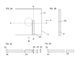
- FIG. 1 is an assembly diagram of a non-contact charging module in the embodiment of the present invention.
- FIGS. 2A to 2D are conceptual diagrams of the non-contact charging module in the embodiment of the present invention.
- FIG. 2A is a top view of the non-contact charging module
- FIG. 2B is a sectional view of the same viewed from an A direction in FIG. 2A
- FIGS. 2C and 2D are sectional views of the non-contact charging module viewed from a B direction in FIG. 2A
- FIGS. 3A to 3D are conceptual diagrams of a magnetic sheet of the non-contact charging module in the embodiment of the present invention.
- FIG. 3A is a top view of the magnetic sheet
- FIG. 3B is a sectional view of the magnetic sheet viewed from an A direction in FIG. 3A
- FIGS. 3C and 3D are sectional views of the magnetic sheet viewed from a B direction in FIG. 3A .
- Non-contact charging module 1 includes plane coil section 2 including a spirally wound conducting wire and magnetic sheet 3 provided so as to face the surface of coil 21 of plane coil section 2.
- plane coil section 2 includes coil 21 including a conducting wire wound toward the radial direction so as to draw a swirl on a surface and terminals 22 and 23 provided at both ends of coil 21.
- Coil 21 includes a conducting wire wound in parallel on a plane.
- a surface formed by the coil is referred to as coil surface.
- a thickness direction is the direction in which plane coil section 2 and magnetic sheet 3 are stacked.
- coil 21 is wound outward from a bore having a diameter of 20 mm.
- the outer diameter of coil 21 is 30 mm. That is, coil 21 is wound in a doughnut shape.
- Coil 21 may be wound in a circular shape or may be wound in a polygonal shape. In the case of the polygonal shape, a corner portion of coil 21 may be bent in a curved line shape.
- Winding the conducting wires to leave a space in between decreases the floating capacity between the conducting wire of an upper stage and the conducting wire of a lower stage, thereby making it possible to minimize the alternating-current resistance of coil 21.
- the thickness of coil 21 can be minimized by winding the conducting wires densely.
- the conducting wire has a circular shape in cross-section, but an conducting wire having a square shape in cross-section may be employed.
- an conducting wire having a square shape in cross-section when used, a gap is formed between adjacent conducting wires. Therefore, stray capacitance between the conducting wires decreases, which in turn makes it possible to reduce the alternating-current resistance of coil 21.
- the alternating-current resistance of coil 21 is lower and transmission efficiency can be increased when coil 21 is wound in one stage rather than being wound in two stages in the thickness direction. This is because, when the conducting wire is wound in two stages, stray capacitance is generated between the conducting wire in the upper stage and the conducting wire in the lower stage. Therefore, it is preferable to wind coil 21 in one stage in as many portions as possible rather than being entirely wound in two stages. Winding coil 21 in one stage makes it possible to reduce the thickness of non-contact charging module 1. It should be noted that, the low alternating-current resistance of coil 21 in this case prevents a loss in coil 21. Improving an L value makes it possible to improve power transmission efficiency of non-contact charging module 1, which is dependent on the L value.
- inner diameter x on the inner side of coil 21 shown in FIG. 1 is 10 mm to 20 mm.
- the outer diameter of coil 21 is about 30 mm. The smaller the inner diameter x, the larger the number of turns of coil 21 can be formed in non-contact charging module 1 of the same size, which in turn makes it possible to improve the L value.
- Terminals 22 and 23 may be arranged close to each other or may be arranged apart from each other. However, when terminals 22 and 23 are arranged apart from each other, non-contact charging module 1 is more easily mounted.
- Magnetic sheet 3 is provided to improve power transmission efficiency of non-contact charging using electromagnetic induction action.
- magnetic sheet 3 includes flat portion 31, center portion 32, which is the center of magnetic sheet 3 and equivalent to the inner diameter of coil 21, and recessed portion 33.
- center portion 32 does not always need to be formed in a protruding shape.
- Recessed portion 33 may be slit 34. Recessed portion 33 or slit 34 is not always necessary. However, as shown in FIGS. 2C and 2D , when recessed portion 33 or slit 34 is provided, the conducting wire from a winding end of coil 21 to terminal 23 can be housed in recessed portion 33 or slit 34.
- recessed portion 33 or slit 34 is formed to be substantially perpendicular to the end of magnetic sheet 3 and overlap a tangential line of the outer circumference of center portion 32. Recessed portion 33 or slit 34 formed in this manner makes it possible to form terminals 22 and 23 without bending the conducting wire. Note that, in this case, the length of recessed portion 33 or slit 34 is about 15 mm to 20 mm. Meanwhile, the length of recessed portion 33 or slit 34 depends on the inner diameter of coil 21. Recessed portion 33 or slit 34 may be formed in a portion where the end of magnetic sheet 3 and the outer circumference of center portion 32 are closest to each other.
- the length of recessed portion 33 or slit 34 is about 5 mm to 10 mm.
- the inner side end of recessed portion 33 or slit 34 is connected to center portion 32.
- Recessed portion 33 or slit 34 may be placed in a different way.
- one of terminals 22 and 23 can be drawn out from the outer circumference of coil 21.
- the other has to be drawn out from the inner side. Therefore, a wound portion of coil 21 and foot portion 24 (see FIG. 4D ) always overlap in the thickness direction. Therefore, recessed portion 33 or slit 34 may be provided in the overlapping portion, and foot portion 24 only is housed in recessed portion 33 or slit 34.
- foot portion 24 means a portion extending from the winding end of coil 21 to terminal 22 or 23. In the case of recessed portion 33, since no through-hole or slit is provided in magnetic sheet 3, it is possible to prevent a magnetic flux from leaking and improve the power transmission efficiency of non-contact charging module 1.
- the cross-sectional shape of recessed portion 33 is not limited to a square shape as shown in FIG. 4C and may be an arc shape or rounded shape.
- magnetic sheet 3 a Ni-Zn ferrite sheet, a Mn-Zn ferrite sheet, a Mg-Zn ferrite sheet, or the like can be used as magnetic sheet 3.
- the ferrite sheet can reduce the alternating-current resistance of coil 21 compared with an amorphous metal magnetic sheet.
- high-saturation magnetic flux density material 3a and high-magnetic permeability material 3b are stacked in magnetic sheet 3. Even when high-saturation magnetic flux density material 3a and high-magnetic permeability material 3b are not stacked, it is advisable to use high-saturation magnetic flux density material 3a having saturation magnetic flux density equal to or higher than 350 mT and thickness of at least 300 ⁇ m.
- coil 21 it is preferable to place coil 21 in a one-stage structure.
- recessed portion 33 or slit 34 is linearly provided in the overlapping portion.
- recessed portion 33 or slit 34 is linear recessed portion 33 or slit 34 that is parallel to a tangential line of the circumference of an inner circumferential circle of the surface of coil 21 and extends in a shortest distance from a winding start or winding end point of the coil surface to the end of magnetic sheet 3.
- the tangential line of the inner circumference of the inner circumferential surface of coil 21 is a tangential line of the inner circumference of an inner circumferential circle in a place where recessed portion 33 or slit 34, which extends from the vicinity of the outer circumference of the inner circumferential circle of the surface of coil 21, is close to the outer circumference of the inner circumferential circle of the surface of coil 21.
- Forming linear portion 33b in this way makes it possible to form terminals 22 and 23 without bending the conducting wire on magnetic sheet 3. That is, when recessed portion 33 or slit 34 is provided, in order to fit the conducting wire in recessed portion 33 or slit 34, the conducting wire has to be bent in the thickness direction from flat portion 31 toward recessed portion 33 or slit 34.
- the conducting wire is not bent on magnetic sheet 3 in a portion where the conducting wire is fit from flat portion 31 toward recessed portion 33 or slit 34, it is possible to achieve a reduction in thickness while maintaining the strength of the conducting wire.
- the length of linear portion 33b is about 15 mm to 20 mm.
- Coil 21 may be wound in a polygonal shape. In that case, it is advisable to provide recessed portion 33 or slit 34 linearly parallel to the shape of a space formed by the inner side end of the surface of coil 21 or a tangential line of the shape and extending in a shortest distance from the winding start or winding end point of the coil surface to the end of magnetic sheet 3.
- Recessed portion 33 or slit 34 that is perpendicular to the tangential line of the circumference of the inner circumferential circle of the surface of coil 21 and extends in a shortest distance from the winding start or winding end point of the coil surface to the end of magnetic sheet 3 may be formed on magnetic sheet 3. Consequently, it is possible to minimize the area where recessed portion 33 or the slit is formed and improve the transmission efficiency of non-contact charging module 1. Stated differently, when recessed portion 33 or slit 34 is provided, a part of magnetic sheet 3 is lost or reduced in thickness. Therefore, there is a concern that a magnetic flux leaks from recessed portion 33 or slit 34 and the power transmission efficiency of the non-contact charging module falls a little, accordingly.
- recessed portion 33 makes it possible to achieve a reduction in thickness while minimizing the leak of the magnetic flux and maintaining the power transmission efficiency of the non-contact charger.
- the length of linear portion 33b is about 5 mm to 10 mm.
- recessed portion 33 or slit 34 is provided on the tangential line of the outer circumference of center portion 32 at a position corresponding to the shortest distance to the end of magnetic sheet 3, recessed portion 33 or slit 34 has a shape parallel to end 3a of magnetic sheet 3.
- coil 21 may be wound in a polygonal shape.
- recessed portion 33 or slit 34 may be perpendicular to the shape of the space formed by the inner side end of the surface of coil 21 or the tangential line of the shape. Therefore, it is advisable to provide recessed portion 33 or slit 34 linearly extending at the shortest distance from the winding start or winding end point of the coil surface to the end of magnetic sheet 3.
- coil 21 is wound in a plane shape from the inner side to the outer side, so that recessed portion 33 or slit 34 extends from the winding start point to the end of magnetic sheet 3.
- recessed portion 33 or slit 34 is parallel to sides of a pair of opposed ends of square magnetic sheet 3 and perpendicular to sides of the other pair of opposed ends.
- magnetic sheet 3 in this embodiment is square.
- the shape of magnetic sheet 3 is not limited to the square shape. Various shapes such as a circular shape and a polygonal shape may be used. Therefore, for example, the shape of magnetic sheet 3 is a polygonal shape and recessed portion 33 or slit 34 is perpendicular to a side that is in contact with one end of recessed portion 33 or slit 34, which makes it possible to minimize the area of recessed portion 33 or slit 34 in a convenient polygonal magnetic sheet.
- the shape of magnetic sheet 3 is the square shape and recessed portion 33 or slit 34 is parallel to the sides of a pair of opposed ends of magnetic sheet 3 and perpendicular to the sides of the other pair of opposed ends. Consequently, it is possible to minimize the area of recessed portion 33 or slit 34 in a most convenient square magnetic sheet.
- recessed portion 33 or slit 34 is provided in a portion where coil 21 and foot portion 24 overlap each other.
- the surface of coil 21 is provided on flat portion 31.
- recessed portion 33 or slit 34 may be provided slightly longer or shorter. However, it is preferable that recessed portion 33 or slit 34 be provided so as to cover at least 80% of the portion where coil 21 and foot portion 24 overlap each other.
- magnetic sheet 3 has a size of about 33 mm ⁇ 33 mm. Thickness d1 of center portion 32 shown in FIG. 2C is 0.2 mm. In FIG. 3C , d2 denotes the thickness of magnetic sheet 3.
- Magnetic sheet 3 includes stacking high-saturation magnetic flux density material 3a, which is stacked on high-magnetic permeability material 3b while the respective thicknesses of high-saturation magnetic flux density material 3a and high-magnetic permeability material 3b are set in such a way that d2, d3, and d4 are equal to 0.6 mm, 0.15 mm, and 0.45 mm, respectively.
- conductive magnetic sheet 3 does not necessarily mean that all portions of magnetic sheet 3 are conductive, and the term also refers to a case where at least a part of magnetic sheet 3 is conductive, for example, as illustrated in FIGS. 3C and 3D where reference numerals 3a and 3b denote a conductive sheet and a nonconductive sheet, respectively.
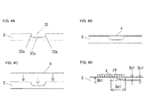
- FIGS. 4A to 4D are diagrams of the magnetic sheet in which the recessed portion is formed and the plane coil section in the embodiment of the present invention.
- FIG. 4A is a sectional view of the recessed portion of the magnetic sheet.
- FIG. 4B is a sectional view of the magnetic sheet and the insulation sheet before bonding.
- FIG. 4C is a sectional view of the magnetic sheet and the insulation sheet after bonding.
- FIG. 4D is a sectional view of the insulation sheet and the foot portion of the coil. These sectional views are sectional views taken along line C-C of the recessed portion shown in FIG. 3A .
- insulation sheet 4 is provided on at least a portion of magnetic sheet 3 where plane coil section 2 is placed.
- insulation sheet 4 is configured to cover the entire surface of magnetic sheet 3, which makes it possible to surely insulate plane coil section 2 and magnetic sheet 3 from each other. Insulation sheet 4 not only bonds plane coil section 2 and magnetic sheet 3 but also insulates plane coil section 2 and magnetic sheet 3 from each other. Therefore, insulation sheet 4 is always interposed between plane coil section 2 and magnetic sheet 3.
- a base material PET, PEN, acrylic, or polyester with an acrylic or silicone adhesive may be used. It is preferable that the dimensional expansion ratio of insulation sheet 4 be 0.05% to 0.1%.
- the term "dimensional expansion ratio” is a ratio expressed by (length after processing-length before processing)/length before processing, and the term “processing” means that insulation sheet 4 is expanded by foot portion 24.
- the diameter of the conducting wire be about 0.3 mm at most when such a form is adopted.
- a small hole may be made in order to remove the air between recessed portion 33 and insulation sheet 4 and increase the elasticity of insulation sheet 4.
- the size of the hole is desirably equal to or larger than 200 ⁇ m.
- the hole is preferably made closer to the center side end of recessed portion 33 or slit 34 and at a position within a range of 1/2 from the center side of the slit length.
- width Da1 of the slit is 1.34 mm
- thickness Db1 of magnetic sheet 3 is 0.6 mm
- diameter Dc1 of the conducting wire is 0.25 mm
- depth Dd1 of recessed portion 33 is 0.3 mm.
- diameter Dc1 (0.25 mm) of the conducting wire is relatively small with respect to thickness Db1 (0.6 mm) of magnetic sheet 3.
- recessed portion 33 is provided on magnetic sheet 3, rather than slit 34. Consequently, the magnetic field can be prevented from easily leaking from magnetic sheet 3 in power transmission.
- diameter Dc of the conducting wire is not greater than 75% of thickness Db1 of magnetic sheet 3
- recessed portion 33 is preferably formed.
- diameter Dc of the conducting wire is not greater than 50% of thickness Db1 of magnetic sheet 3. It is preferable that width Da1 of the slit be at least three times as large as diameter Dc1 of the conducting wire. When width Da1 of the slit is at least three times as large as diameter Dc1 of the conducting wire, insulation sheet 4 can sufficiently house foot portion 24 in recessed portion 33.
- the conducting wire is housed in first slit 34 with insulation sheet 4 interposed therebetween.
- the structure described above is particularly useful for a secondary side non-contact charging module, which is a reception side. That is, since the value of an electric current flowing through a coil and the value of voltage of the electric current are relatively small in the secondary side non-contact charging module, such a small diameter of conducting wire, which is 0.25 mm, is sufficient. On the other hand, since a housing itself of the secondary side non-contact charging module is preferably reduced in size, a distance between metal closest to plane coil section 2 and plane coil section 2 is extremely small compared with a primary side non-contact charging module. Therefore, in order to sufficiently prevent the influence of the metal, magnetic sheet 3 is thick compared with the primary side non-contact charging module.
- the diameter of the conducting wire is small and the thickness of magnetic sheet 3 is large compared with the primary side non-contact charging module. Therefore, recessed portion 33 is often formed on magnetic sheet 3.
- the conductive conducting wire approaches to bottom surface 33c of recessed portion 33. Since insulation sheet 4 is provided with slit 41, insulation sheet 4 needs to have elasticity.
- the thickness of insulation sheet 4 is set to a small thickness, which is 10 ⁇ m.
- the thickness of insulation sheet 4 is preferably not greater than 5 to 20 ⁇ m.
- the non-contact charging module includes the plane coil section including the spirally wound conducting wire, the magnetic sheet provided so as to face the coil surface with the insulation sheet interposed therebetween, and the recessed portion or the slit provided on the magnetic sheet and extending from the winding start or winding end point of the coil surface to the end of the magnetic sheet.
- the magnetic sheet at least a part of the portion where the recessed portion or the slit is formed is conductive.
- the conducting wire is pressed against the insulation sheet into the recessed portion or the slit and is thereby housed in the recessed portion or the slit. Therefore, it is possible to achieve a reduction in thickness in a state in which the conducting wire and the magnetic sheet are surely insulated from each other.
- the width of the recessed portion is at least three times as large as the diameter of the conducting wire, the conducting wire is surely housed in the recessed portion by the elasticity of the insulation sheet. Therefore, it is possible to achieve a reduction in thickness in a state in which the conducting wire and the magnetic sheet are surely insulated from each other.
- the conducting wire Since the diameter of the conducting wire is smaller than 0.3 mm and the thickness of the insulation sheet is between 5 and 20 ⁇ m, the conducting wire is surely housed in the recessed portion by the elasticity of the insulation sheet. Therefore, it is possible to achieve a reduction in thickness in a state in which the conducting wire and the magnetic sheet are surely insulated from each other.
- magnetic sheet 3 and plane coil section 2 may be insulated by the same method as that used in the case of recessed portion 33 or can be insulated by a method to be described below.
- the method to be described below can be applied to recessed portion 33 as well, but the method described above is preferable.
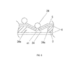
- FIG. 5 is an enlarged sectional view of the magnetic sheet in which the slit is formed and the plane coil section in the embodiment of the present invention.
- FIGS. 6 are sectional views of the magnetic sheet in which the slit is formed and the plane coil section in the embodiment of the present invention.
- FIG. 6A is a sectional view taken along line C-C of the insulation sheet in which the slit is formed instead of the recessed portion in FIG. 3A .
- FIG. 6B is a sectional view taken along line D-D of the insulation sheet in which the slit is formed instead of the recessed portion in FIG. 3A .
- Non-contact charging module 1 in this embodiment includes plane coil section 2 including the spirally wound conducting wire, magnetic sheet 3 provided so as to face the surface of coil 21 with insulation sheet 4 interposed therebetween, and first slit 34 provided on the magnetic sheet and extending from the winding start or winding end point of the coil surface to the end of magnetic sheet 3.
- Second slit 41 (a cut) is provided on insulation sheet 4 in a position corresponding to (facing) first slit 34. Foot portion 24 of the conducting wire is housed in first slit 34 with insulation sheet 4 interposed therebetween.
- insulation sheets 4 are respectively provided on both surfaces of magnetic sheet 3. Since second slit 41 is the cut, first slit 34 is thicker than second slit 41.
- width Da2 of the slit is 1.34 mm
- thickness Db2 of magnetic sheet 3 is 0.46 mm
- diameter Dc2 of the conducting wire is 0.35 mm.
- Width Da2 (1.34 mm) of the slit is at least twice as large as thickness Db2 (0.46 mm) of magnetic sheet 3 and line diameter Dc2 (0.35 mm) of the conducting wire. That is, since the thickness of sidewall 34a is thickness Db2 (0.46 mm) of magnetic sheet 3 and sidewall 34a is present on both left and right sides of the conducting wire, a portion of insulation sheet 4 pressed into slit 34 needs to be twice or more.
- Width Da1 of the slit is preferably at least three times as large as diameter Dc1 of the conducting wire.
- the conducting wire is housed in first slit 34 with insulation sheet 4 interposed therebetween.
- the structure described above is particularly useful for the primary side non-contact charging module, which is the transmission side. That is, since the value of an electric current flowing through the coil and the value of voltage of the electric current are large in the primary side non-contact charging module, the diameter of the conducting wire has a large thickness, which is 0.35 mm. On the other hand, since a housing itself of the primary side non-contact charging module is large, a distance between metal closest to plane coil section 2 and plane coil section 2 is large compared with the secondary side non-contact charging module. Therefore, magnetic sheet 3 is thin compared with the secondary side non-contact charging module. As a result, the diameter of the conducting wire is large and the thickness of magnetic sheet 3 is small compared with the secondary side non-contact charging module.
- slit 34 is often formed on magnetic sheet 3.
- insulation sheet 4 different from insulation sheet 4 in which slit 41 is formed is bonded. Since slit 41 is provided, insulation sheet 4 does not need to have elasticity. Therefore, in this embodiment, the thickness of insulation sheet 4 is set to a large thickness, which is 30 ⁇ m.
- the thickness of insulation sheet 4 is preferably 20 to 50 ⁇ m such that there is no reduction in strength even if the slit is formed.
- a base material PET, PEN, acrylic, or polyester an acrylic or silicone adhesive is preferably used for insulation sheet 4.
- the diameter of the conducting wire is smaller than the thickness of the magnetic sheet.
- the non-contact charging module includes the plane coil section including the spirally wound conducting wire, the magnetic sheet provided so as to face the coil surface with the insulation sheet interposed therebetween, and the first slit provided on the magnetic sheet and extending from the winding start or winding end point of the coil surface to the end of the magnetic sheet. At least a part of the portion of the magnetic sheet where the first slit is formed is conductive. The second slit is provided on the insulation sheet in the position corresponding to the first slit. The conducting wire is housed in the first slit with the insulation sheet interposed therebetween. Therefore, it is possible to achieve a reduction in thickness in a state in which the conducting wire and the magnetic sheet are surely insulated from each other.
- the width of slit 34 is at least twice as large as the diameter of the conducting wire. Therefore, the insulation sheet is surely interposed between the conducting wire and the magnetic sheet, which makes it possible to surely insulate the conducting wire and the magnetic sheet from each other and achieve a reduction in thickness.
- the width of slit 34 is at least twice as large as the thickness of the magnetic sheet. Therefore, the insulation sheet is surely interposed between the conducting wire and the magnetic sheet, which makes it possible to surely insulate the conducting wire and the magnetic sheet from each other and achieve a reduction in thickness.
- the diameter of the conducting wire is smaller than the thickness of the magnetic sheet, and the thickness of the insulation sheet is 20 to 50 ⁇ m. Therefore, the insulation sheet is surely interposed between the conducting wire and the magnetic sheet, which makes it possible to surely insulate the conducting wire and the magnetic sheet from each other and achieve a reduction in thickness.
- coil 21 is not limited to be wound in an annular shape and may be wound in a square shape or a polygonal shape. Furthermore, the effect of this application can also be obtained by performing winding in such a way that the inner side is wound in a plurality of stages one on top of another and the outer side is wound in the number of stages smaller than the number of stages for the inner side, for example, a three-stage structure for the inner side and a two-stage structure for the outer side.
- a non-contact transmitting apparatus includes a charger including a power transmission coil and a magnetic sheet and a main apparatus including a power reception coil and a magnetic sheet.
- the main apparatus is an electronic apparatus such as a cellular phone.
- a circuit on the charger side includes a rectifying and smoothing circuit section, a voltage conversion circuit section, an oscillation circuit section, a display circuit section, a control circuit section, and the power transmission coil.
- a circuit on the main apparatus side includes the power reception coil, a rectifying circuit section, a control circuit section, and a load L mainly formed of a secondary battery.
- Power transmission from the charger to the main apparatus is performed using electromagnetic induction action between the power transmission coil of the charger, which is the primary side and the power reception coil of the main apparatus, which is the secondary side.
- the non-contact charger in this embodiment includes the non-contact charging module explained above. Therefore, it is possible to reduce the size and the thickness of the non-contact charger in a state in which the sectional area of the plane coil section is sufficiently secured with improved power transmission efficiency.
- the non-contact charging module With the non-contact charging module according to the present invention, it is possible to reduce the thickness of the non-contact charging module in a state in which the sectional area of the plane coil section is sufficiently secured. Therefore, the non-contact charging module is useful as non-contact charging modules of various electronic apparatuses including portable terminals such as a cellular phone and a portable computer and portable apparatuses such as a video camera.
Abstract
Description
- The present invention relates to a non-contact charging module and a non-contact charger including a magnetic sheet, and a plane coil section including a wound conducting wire.
- In recent years, use of a system which enables charging of a main apparatus by a charger in a non-contact manner has become widespread. Such a system includes a power transmission coil on the charger side, and a power reception coil on the main apparatus side. Electromagnetic induction is generated between the coils, whereby electric power is transmitted from the charger side to the main apparatus side. In addition, it has been proposed to apply a portable terminal apparatus or the like as the main apparatus.
- The main apparatus such as the portable terminal apparatus and the charger are preferably reduced in thickness and size. In order to meet such a demand, a non-contact charging module including plane coil sections serving as a power transmission coil and a power reception coil, and magnetic sheets may be employed as disclosed in Japanese Patent Application Laid-Open No.
2006-42519 -
-
PTL 1
Japanese Patent Application Laid-Open No.2006-42519 - However, in the non-contact module including a plane coil section formed of one conducting wire and a magnetic sheet entirely formed in a plane shape as disclosed in
PTL 1, the winding start portion or winding end portion of the coil is located under the inner side of the coil in some cases. In such cases, a wound portion of the coil and a portion between the winding start portion or winding end portion of the coil and a terminal overlap in the thickness direction as in a case where a plurality of conducting wires is used. Such overlapping prevents a reduction in thickness of the non-contact charging module as a result. - In addition, since some magnetic sheet is conductive, insulation between the conducting wire and the magnetic sheet is important when such a conductive magnetic sheet is used.
- Therefore, in view of the above-mentioned problems, it is an object of the present invention to achieve a reduction in thickness in a state in which the conducting wire and the magnetic sheet are surely insulated from each other.
- In order to solve the problems, an aspect of the present invention provides a non-contact charging module including: a plane coil section including a wound conducting wire; a magnetic sheet having electric conductivity on which the plane coil section is placed with an insulation sheet interposed therebetween; and a recessed portion or a slit provided in the magnetic sheet and extending from a winding start point of the plane coil section to an end of the magnetic sheet, in which the conducting wire of the plane coil section is pressed against the insulation sheet into the recessed portion or the slit and is thereby housed in the recessed portion or the slit, and the conducting wire of the plane coil section is insulated from the magnetic sheet having electric conductivity because of the insulation sheet.
- According to the present invention, it is possible to achieve a reduction in thickness in a state in which the conducting wire and the magnetic sheet are surely insulated from each other.
-
-
FIG. 1 is an assembly diagram of a non-contact charging module in an embodiment of the present invention; -
FIGS. 2A to 2D are conceptual diagrams of the non-contact charging module in the embodiment of the present invention; -
FIGS. 3A to 3D are conceptual diagrams of a magnetic sheet of the non-contact charging module in the embodiment of the present invention; -
FIGS. 4A to 4D are diagrams of the magnetic sheet in which a recessed portion is formed and a plane coil section in the embodiment of the present invention; -
FIG. 5 is an enlarged sectional view of the magnetic sheet in which a slit is formed and the plane coil section in the embodiment of the present invention; and -
FIGS. 6A and 6B are sectional views of the magnetic sheet in which the slit is formed and the plane coil section in the embodiment of the present invention. - The invention as recited in
claim 1 is a non-contact charging module including: a plane coil section including a wound conducting wire; a magnetic sheet having electric conductivity on which the plane coil section is placed with an insulation sheet interposed therebetween; and a recessed portion or a slit provided in the magnetic sheet and extending from a winding start point of the plane coil section to an end of the magnetic sheet, in which the conducting wire of the plane coil section is housed in the recessed portion or the slit with the insulation sheet pressed into the recessed portion or the slit, and the conducting wire of the plane coil section is insulated from the magnetic sheet having electric conductivity because of the insulation sheet. Thus, it is possible to achieve a reduction in thickness in a state in which the conducting wire and the magnetic sheet are surely insulated from each other. - The invention as recited in
claim 2 is the non-contact charging module according toclaim 1, in which a width of the recessed portion or the slit is at least three times as large as a diameter of the conducting wire. The conducting wire is surely housed in the recessed portion by the elasticity of the insulation sheet. Therefore, it is possible to realize a reduction in thickness in a state in which the conducting wire and the magnetic sheet are surely insulated from each other. - The invention as recited in
claim 3 is the non-contact charging module according toclaim 1, in which a diameter of the conducting wire is smaller than 0.3 mm and a thickness of the insulation sheet is 5 to 20 mm. The conducting wire is surely housed in the recessed portion by the elasticity of the insulation sheet. Therefore, it is possible to realize a reduction in thickness in a state in which the conducting wire and the magnetic sheet are surely insulated from each other. - The invention as recited in
claim 4 is the non-contact charging module according toclaim 1, in which a through-hole smaller than a diameter of the conducting wire is made in a portion of the insulation sheet facing the recessed portion or the slit. Even when the elasticity of the insulation sheet is insufficient, the conducting wire is surely housed in the recessed portion by the elasticity of the insulation sheet. Therefore, it is possible to realize a reduction in thickness in a state in which the conducting wire and the magnetic sheet are surely insulated from each other. - The invention as recited in
claim 5 is the non-contact charging module according toclaim 1, in which a dimensional expansion ratio of the insulation sheet is 0.05% to 0.1%. The conducting wire is housed in the recessed portion by the elasticity of the insulation sheet even if no hole or the like is formed in the insulation sheet. Therefore, it is possible to realize a reduction in thickness in a state in which the conducting wire and the magnetic sheet are surely insulated from each other. - The invention as recited in claim 6 is the non-contact charging module according to
claim 1, in which the insulation sheet includes a cut in a position corresponding to the recessed portion or the slit, the conducting wire is housed in the recessed portion or the slit so as to interpose the insulation sheet between the conducting wire and the magnetic sheet, and the conducting wire of the plane coil section is insulated from the magnetic sheet having electric conductivity because of the insulation sheet. Even if a relatively thick conducting wire is used, it is possible to realize a reduction in thickness in a state in which the conducting wire and the magnetic sheet are surely insulated from each other. - The invention as recited in claim 7 is the non-contact charging module according to claim 6, in which a diameter of the conducting wire of the plane coil section is smaller than a thickness of the magnetic sheet, and a thickness of the magnetic sheet is 20 to 50 µm. Even if a relatively thick conducting wire is used, it is possible to realize a reduction in thickness in a state in which the conducting wire and the magnetic sheet are surely insulated from each other.
- The invention as recited in claim 8 is the non-contact charging module according to claim 6, in which a width of the recessed portion or the slit is at least twice as large as a diameter of the conducting wire. Since the insulation sheet is surely interposed between the conducting wire and the magnetic sheet, it is possible to surely insulate the conducting wire and the magnetic sheet from each other and realize a reduction in thickness.
- The invention as recited in claim 9 is the non-contact charging module according to claim 6, in which a width of the recessed portion or the slit is at least twice as large as a thickness of the magnetic sheet. Since the insulation sheet is surely interposed between the conducting wire and the magnetic sheet, it is possible to surely insulate the conducting wire and the magnetic sheet from each other and realize a reduction in thickness.
- The invention as recited in claim 10 is a non-contact charger comprising the non-contact charging module according to
claim 1. It is possible to realize a reduction in thickness in a state in which the conducting wire and the magnetic sheet are surely insulated from each other. - The invention as recited in claim 11 is an electronic apparatus comprising the non-contact charging module according to
claim 1. It is possible to realize a reduction in thickness in a state in which the conducting wire and the magnetic sheet are surely insulated from each other. - An embodiment of the present invention is explained below with reference to the drawings.
FIG. 1 is an assembly diagram of a non-contact charging module in the embodiment of the present invention.FIGS. 2A to 2D are conceptual diagrams of the non-contact charging module in the embodiment of the present invention.FIG. 2A is a top view of the non-contact charging module,FIG. 2B is a sectional view of the same viewed from an A direction inFIG. 2A, and FIGS. 2C and 2D are sectional views of the non-contact charging module viewed from a B direction inFIG. 2A .FIGS. 3A to 3D are conceptual diagrams of a magnetic sheet of the non-contact charging module in the embodiment of the present invention.FIG. 3A is a top view of the magnetic sheet,FIG. 3B is a sectional view of the magnetic sheet viewed from an A direction inFIG. 3A, and FIGS. 3C and 3D are sectional views of the magnetic sheet viewed from a B direction inFIG. 3A . -
Non-contact charging module 1 according to the present invention includesplane coil section 2 including a spirally wound conducting wire andmagnetic sheet 3 provided so as to face the surface ofcoil 21 ofplane coil section 2. - As shown in
FIG. 1 ,plane coil section 2 includescoil 21 including a conducting wire wound toward the radial direction so as to draw a swirl on a surface andterminals coil 21.Coil 21 includes a conducting wire wound in parallel on a plane. A surface formed by the coil is referred to as coil surface. A thickness direction is the direction in whichplane coil section 2 andmagnetic sheet 3 are stacked. In this embodiment,coil 21 is wound outward from a bore having a diameter of 20 mm. The outer diameter ofcoil 21 is 30 mm. That is,coil 21 is wound in a doughnut shape.Coil 21 may be wound in a circular shape or may be wound in a polygonal shape. In the case of the polygonal shape, a corner portion ofcoil 21 may be bent in a curved line shape. - Winding the conducting wires to leave a space in between decreases the floating capacity between the conducting wire of an upper stage and the conducting wire of a lower stage, thereby making it possible to minimize the alternating-current resistance of
coil 21. In addition, the thickness ofcoil 21 can be minimized by winding the conducting wires densely. - As shown in
FIG. 2A , in this embodiment, the conducting wire has a circular shape in cross-section, but an conducting wire having a square shape in cross-section may be employed. However, compared with the conducting wire having a square shape in cross-section, when the conducting wire having a circular shape in cross-section is used, a gap is formed between adjacent conducting wires. Therefore, stray capacitance between the conducting wires decreases, which in turn makes it possible to reduce the alternating-current resistance ofcoil 21. - In addition, the alternating-current resistance of
coil 21 is lower and transmission efficiency can be increased whencoil 21 is wound in one stage rather than being wound in two stages in the thickness direction. This is because, when the conducting wire is wound in two stages, stray capacitance is generated between the conducting wire in the upper stage and the conducting wire in the lower stage. Therefore, it is preferable to windcoil 21 in one stage in as many portions as possible rather than being entirely wound in two stages. Windingcoil 21 in one stage makes it possible to reduce the thickness ofnon-contact charging module 1. It should be noted that, the low alternating-current resistance ofcoil 21 in this case prevents a loss incoil 21. Improving an L value makes it possible to improve power transmission efficiency ofnon-contact charging module 1, which is dependent on the L value. - In this embodiment, inner diameter x on the inner side of
coil 21 shown inFIG. 1 is 10 mm to 20 mm. The outer diameter ofcoil 21 is about 30 mm. The smaller the inner diameter x, the larger the number of turns ofcoil 21 can be formed innon-contact charging module 1 of the same size, which in turn makes it possible to improve the L value. -
Terminals terminals non-contact charging module 1 is more easily mounted. -
Magnetic sheet 3 is provided to improve power transmission efficiency of non-contact charging using electromagnetic induction action. As shown inFIG. 2A ,magnetic sheet 3 includesflat portion 31,center portion 32, which is the center ofmagnetic sheet 3 and equivalent to the inner diameter ofcoil 21, and recessedportion 33. As shown inFIGS. 3A to 3D ,center portion 32 does not always need to be formed in a protruding shape. Recessedportion 33 may be slit 34. Recessedportion 33 or slit 34 is not always necessary. However, as shown inFIGS. 2C and 2D , when recessedportion 33 or slit 34 is provided, the conducting wire from a winding end ofcoil 21 toterminal 23 can be housed in recessedportion 33 or slit 34. Therefore, a reduction in size in the thickness direction is made possible. Specifically, recessedportion 33 or slit 34 is formed to be substantially perpendicular to the end ofmagnetic sheet 3 and overlap a tangential line of the outer circumference ofcenter portion 32. Recessedportion 33 or slit 34 formed in this manner makes it possible to formterminals portion 33 or slit 34 is about 15 mm to 20 mm. Meanwhile, the length of recessedportion 33 or slit 34 depends on the inner diameter ofcoil 21. Recessedportion 33 or slit 34 may be formed in a portion where the end ofmagnetic sheet 3 and the outer circumference ofcenter portion 32 are closest to each other. Consequently, it is possible to minimize the area where recessedportion 33 or slit 34 is formed and to improve the transmission efficiency ofnon-contact charging module 1. Note that, in this case, the length of recessedportion 33 or slit 34 is about 5 mm to 10 mm. In both of the placements, the inner side end of recessedportion 33 or slit 34 is connected to centerportion 32. Recessedportion 33 or slit 34 may be placed in a different way. Stated differently, it is preferable to placecoil 21 in a one-stage structure. In this case, it is possible to form all turns in the radial direction ofcoil 21 in the one-stage structure or to form a part of the turns in the one-stage structure while forming the other parts in a two-stage structure. Therefore, one ofterminals coil 21. However, the other has to be drawn out from the inner side. Therefore, a wound portion ofcoil 21 and foot portion 24 (seeFIG. 4D ) always overlap in the thickness direction. Therefore, recessedportion 33 or slit 34 may be provided in the overlapping portion, andfoot portion 24 only is housed in recessedportion 33 or slit 34. Note thatfoot portion 24 means a portion extending from the winding end ofcoil 21 toterminal portion 33, since no through-hole or slit is provided inmagnetic sheet 3, it is possible to prevent a magnetic flux from leaking and improve the power transmission efficiency ofnon-contact charging module 1. On the other hand, in the case ofslit 34, it is easy to formmagnetic sheet 3. In the case of recessedportion 33, the cross-sectional shape of recessedportion 33 is not limited to a square shape as shown inFIG. 4C and may be an arc shape or rounded shape. - In this embodiment, as
magnetic sheet 3, a Ni-Zn ferrite sheet, a Mn-Zn ferrite sheet, a Mg-Zn ferrite sheet, or the like can be used. The ferrite sheet can reduce the alternating-current resistance ofcoil 21 compared with an amorphous metal magnetic sheet. - As shown in
FIGS. 3C and 3D , at least high-saturation magneticflux density material 3a and high-magnetic permeability material 3b are stacked inmagnetic sheet 3. Even when high-saturation magneticflux density material 3a and high-magnetic permeability material 3b are not stacked, it is advisable to use high-saturation magneticflux density material 3a having saturation magnetic flux density equal to or higher than 350 mT and thickness of at least 300 µm. - It is preferable to place
coil 21 in a one-stage structure. In this case, it is possible to form all turns in the radial direction ofcoil 21 in the one-stage structure or to form a part of the turns in the one-stage structure while forming the other parts in a two-stage structure. Therefore, one ofterminals coil 21. However, the other has to be drawn out from the inner side. Therefore, a wound portion ofcoil 21 andfoot portion 24 always overlap in the thickness direction. - Therefore, in the present invention, recessed
portion 33 or slit 34 is linearly provided in the overlapping portion. In particular, recessedportion 33 or slit 34 is linear recessedportion 33 or slit 34 that is parallel to a tangential line of the circumference of an inner circumferential circle of the surface ofcoil 21 and extends in a shortest distance from a winding start or winding end point of the coil surface to the end ofmagnetic sheet 3. The tangential line of the inner circumference of the inner circumferential surface ofcoil 21 is a tangential line of the inner circumference of an inner circumferential circle in a place where recessedportion 33 or slit 34, which extends from the vicinity of the outer circumference of the inner circumferential circle of the surface ofcoil 21, is close to the outer circumference of the inner circumferential circle of the surface ofcoil 21. Forming linear portion 33b in this way makes it possible to formterminals magnetic sheet 3. That is, when recessedportion 33 or slit 34 is provided, in order to fit the conducting wire in recessedportion 33 or slit 34, the conducting wire has to be bent in the thickness direction fromflat portion 31 toward recessedportion 33 or slit 34. Therefore, since the conducting wire is not bent onmagnetic sheet 3 in a portion where the conducting wire is fit fromflat portion 31 toward recessedportion 33 or slit 34, it is possible to achieve a reduction in thickness while maintaining the strength of the conducting wire. Note that, in this case, the length of linear portion 33b is about 15 mm to 20 mm.Coil 21 may be wound in a polygonal shape. In that case, it is advisable to provide recessedportion 33 or slit 34 linearly parallel to the shape of a space formed by the inner side end of the surface ofcoil 21 or a tangential line of the shape and extending in a shortest distance from the winding start or winding end point of the coil surface to the end ofmagnetic sheet 3. - Recessed
portion 33 or slit 34 that is perpendicular to the tangential line of the circumference of the inner circumferential circle of the surface ofcoil 21 and extends in a shortest distance from the winding start or winding end point of the coil surface to the end ofmagnetic sheet 3 may be formed onmagnetic sheet 3. Consequently, it is possible to minimize the area where recessedportion 33 or the slit is formed and improve the transmission efficiency ofnon-contact charging module 1. Stated differently, when recessedportion 33 or slit 34 is provided, a part ofmagnetic sheet 3 is lost or reduced in thickness. Therefore, there is a concern that a magnetic flux leaks from recessedportion 33 or slit 34 and the power transmission efficiency of the non-contact charging module falls a little, accordingly. Therefore, minimizing the area where recessedportion 33 is formed makes it possible to achieve a reduction in thickness while minimizing the leak of the magnetic flux and maintaining the power transmission efficiency of the non-contact charger. Note that, in this case, the length of linear portion 33b is about 5 mm to 10 mm. Note that, since recessedportion 33 or slit 34 is provided on the tangential line of the outer circumference ofcenter portion 32 at a position corresponding to the shortest distance to the end ofmagnetic sheet 3, recessedportion 33 or slit 34 has a shape parallel to end 3a ofmagnetic sheet 3. Note thatcoil 21 may be wound in a polygonal shape. In that case, recessedportion 33 or slit 34 may be perpendicular to the shape of the space formed by the inner side end of the surface ofcoil 21 or the tangential line of the shape. Therefore, it is advisable to provide recessedportion 33 or slit 34 linearly extending at the shortest distance from the winding start or winding end point of the coil surface to the end ofmagnetic sheet 3. Note that, in general,coil 21 is wound in a plane shape from the inner side to the outer side, so that recessedportion 33 or slit 34 extends from the winding start point to the end ofmagnetic sheet 3. - In
FIGS. 2 and3 , for example, recessedportion 33 or slit 34 is parallel to sides of a pair of opposed ends of squaremagnetic sheet 3 and perpendicular to sides of the other pair of opposed ends. This is becausemagnetic sheet 3 in this embodiment is square. However, the shape ofmagnetic sheet 3 is not limited to the square shape. Various shapes such as a circular shape and a polygonal shape may be used. Therefore, for example, the shape ofmagnetic sheet 3 is a polygonal shape and recessedportion 33 or slit 34 is perpendicular to a side that is in contact with one end of recessedportion 33 or slit 34, which makes it possible to minimize the area of recessedportion 33 or slit 34 in a convenient polygonal magnetic sheet. In particular, the shape ofmagnetic sheet 3 is the square shape and recessedportion 33 or slit 34 is parallel to the sides of a pair of opposed ends ofmagnetic sheet 3 and perpendicular to the sides of the other pair of opposed ends. Consequently, it is possible to minimize the area of recessedportion 33 or slit 34 in a most convenient square magnetic sheet. - Therefore, recessed
portion 33 or slit 34 is provided in a portion wherecoil 21 andfoot portion 24 overlap each other. The surface ofcoil 21 is provided onflat portion 31. Note that recessedportion 33 or slit 34 may be provided slightly longer or shorter. However, it is preferable that recessedportion 33 or slit 34 be provided so as to cover at least 80% of the portion wherecoil 21 andfoot portion 24 overlap each other. - In
FIGS. 2 and3 ,magnetic sheet 3 has a size of about 33 mm × 33 mm. Thickness d1 ofcenter portion 32 shown inFIG. 2C is 0.2 mm. InFIG. 3C , d2 denotes the thickness ofmagnetic sheet 3.Magnetic sheet 3 includes stacking high-saturation magneticflux density material 3a, which is stacked on high-magnetic permeability material 3b while the respective thicknesses of high-saturation magneticflux density material 3a and high-magnetic permeability material 3b are set in such a way that d2, d3, and d4 are equal to 0.6 mm, 0.15 mm, and 0.45 mm, respectively. - Next, insulation between
magnetic sheet 3 andplane coil section 2 in the case of conductivemagnetic sheet 3 is explained. First, a description will be provided regarding a case where recessedportion 33 is formed. Note that the term "conductivemagnetic sheet 3" does not necessarily mean that all portions ofmagnetic sheet 3 are conductive, and the term also refers to a case where at least a part ofmagnetic sheet 3 is conductive, for example, as illustrated inFIGS. 3C and 3D wherereference numerals -
FIGS. 4A to 4D are diagrams of the magnetic sheet in which the recessed portion is formed and the plane coil section in the embodiment of the present invention.FIG. 4A is a sectional view of the recessed portion of the magnetic sheet.FIG. 4B is a sectional view of the magnetic sheet and the insulation sheet before bonding.FIG. 4C is a sectional view of the magnetic sheet and the insulation sheet after bonding.FIG. 4D is a sectional view of the insulation sheet and the foot portion of the coil. These sectional views are sectional views taken along line C-C of the recessed portion shown inFIG. 3A . - In this embodiment, since
magnetic sheet 3 is conductive,sidewall 33a andbottom surface 33c of recessedportion 33 are also conductive. Therefore, the conducting wire andfoot portion 24 thereof should not be in contact with any one ofsidewall 33a andbottom surface 33c of recessedportion 33. Therefore,insulation sheet 4 is bonded at least onto the surface side of themagnetic sheet 3 wherecoil 21 is to be placed.Plane coil section 2 is placed oninsulation sheet 4. At this point,foot portion 24 presses downinsulation sheet 4 corresponding to recessedportion 33 and is housed in recessedportion 33. Consequently, it is possible to bringfoot portion 24 into contact withcoil 21 and to housefoot portion 24 in recessedportion 33. In order to insulateplane coil section 2 andmagnetic sheet 3 from each other,insulation sheet 4 is provided on at least a portion ofmagnetic sheet 3 whereplane coil section 2 is placed. Preferably,insulation sheet 4 is configured to cover the entire surface ofmagnetic sheet 3, which makes it possible to surely insulateplane coil section 2 andmagnetic sheet 3 from each other.Insulation sheet 4 not only bondsplane coil section 2 andmagnetic sheet 3 but also insulatesplane coil section 2 andmagnetic sheet 3 from each other. Therefore,insulation sheet 4 is always interposed betweenplane coil section 2 andmagnetic sheet 3. - In this embodiment, a base material PET, PEN, acrylic, or polyester with an acrylic or silicone adhesive may be used. It is preferable that the dimensional expansion ratio of
insulation sheet 4 be 0.05% to 0.1%. The term "dimensional expansion ratio" is a ratio expressed by (length after processing-length before processing)/length before processing, and the term "processing" means thatinsulation sheet 4 is expanded byfoot portion 24. - It is preferable that the diameter of the conducting wire be about 0.3 mm at most when such a form is adopted.
- It should be noted that a small hole may be made in order to remove the air between recessed
portion 33 andinsulation sheet 4 and increase the elasticity ofinsulation sheet 4. When a small hole is made, the size of the hole is desirably equal to or larger than 200 µm. The hole is preferably made closer to the center side end of recessedportion 33 or slit 34 and at a position within a range of 1/2 from the center side of the slit length. - In this embodiment, width Da1 of the slit is 1.34 mm, thickness Db1 of
magnetic sheet 3 is 0.6 mm, diameter Dc1 of the conducting wire is 0.25 mm, and depth Dd1 of recessedportion 33 is 0.3 mm. In this case, since diameter Dc1 (0.25 mm) of the conducting wire is relatively small with respect to thickness Db1 (0.6 mm) ofmagnetic sheet 3. For this reason, recessedportion 33 is provided onmagnetic sheet 3, rather than slit 34. Consequently, the magnetic field can be prevented from easily leaking frommagnetic sheet 3 in power transmission. When diameter Dc of the conducting wire is not greater than 75% of thickness Db1 ofmagnetic sheet 3, recessedportion 33 is preferably formed. More preferably, diameter Dc of the conducting wire is not greater than 50% of thickness Db1 ofmagnetic sheet 3. It is preferable that width Da1 of the slit be at least three times as large as diameter Dc1 of the conducting wire. When width Da1 of the slit is at least three times as large as diameter Dc1 of the conducting wire,insulation sheet 4 can sufficiently housefoot portion 24 in recessedportion 33. - In the manner described above, the conducting wire is housed in
first slit 34 withinsulation sheet 4 interposed therebetween. - The structure described above is particularly useful for a secondary side non-contact charging module, which is a reception side. That is, since the value of an electric current flowing through a coil and the value of voltage of the electric current are relatively small in the secondary side non-contact charging module, such a small diameter of conducting wire, which is 0.25 mm, is sufficient. On the other hand, since a housing itself of the secondary side non-contact charging module is preferably reduced in size, a distance between metal closest to plane
coil section 2 andplane coil section 2 is extremely small compared with a primary side non-contact charging module. Therefore, in order to sufficiently prevent the influence of the metal,magnetic sheet 3 is thick compared with the primary side non-contact charging module. As a result, the diameter of the conducting wire is small and the thickness ofmagnetic sheet 3 is large compared with the primary side non-contact charging module. Therefore, recessedportion 33 is often formed onmagnetic sheet 3. In the case of recessedportion 33, when pressed into recessedportion 33, the conductive conducting wire approaches tobottom surface 33c of recessedportion 33. Sinceinsulation sheet 4 is provided withslit 41,insulation sheet 4 needs to have elasticity. In this embodiment, the thickness ofinsulation sheet 4 is set to a small thickness, which is 10 µm. The thickness ofinsulation sheet 4 is preferably not greater than 5 to 20 µm. - That is, the non-contact charging module includes the plane coil section including the spirally wound conducting wire, the magnetic sheet provided so as to face the coil surface with the insulation sheet interposed therebetween, and the recessed portion or the slit provided on the magnetic sheet and extending from the winding start or winding end point of the coil surface to the end of the magnetic sheet. In the magnetic sheet, at least a part of the portion where the recessed portion or the slit is formed is conductive. The conducting wire is pressed against the insulation sheet into the recessed portion or the slit and is thereby housed in the recessed portion or the slit. Therefore, it is possible to achieve a reduction in thickness in a state in which the conducting wire and the magnetic sheet are surely insulated from each other.
- Since the width of the recessed portion is at least three times as large as the diameter of the conducting wire, the conducting wire is surely housed in the recessed portion by the elasticity of the insulation sheet. Therefore, it is possible to achieve a reduction in thickness in a state in which the conducting wire and the magnetic sheet are surely insulated from each other.
- Since the diameter of the conducting wire is smaller than 0.3 mm and the thickness of the insulation sheet is between 5 and 20 µm, the conducting wire is surely housed in the recessed portion by the elasticity of the insulation sheet. Therefore, it is possible to achieve a reduction in thickness in a state in which the conducting wire and the magnetic sheet are surely insulated from each other.
- Even when the elasticity of the insulation sheet is insufficient, making a through-hole smaller than the diameter of the conducting wire in a portion of the insulation sheet facing the recessed portion or slit allows the conducting wire to be surely housed in the recessed portion by the elasticity of the insulation sheet. Therefore, it is possible to achieve a reduction in thickness in a state in which the conducting wire and the magnetic sheet are surely insulated from each other.
- Next, a description will be provided regarding a case where slit 34 is formed. In the case of
slit 34,magnetic sheet 3 andplane coil section 2 may be insulated by the same method as that used in the case of recessedportion 33 or can be insulated by a method to be described below. The method to be described below can be applied to recessedportion 33 as well, but the method described above is preferable. -
FIG. 5 is an enlarged sectional view of the magnetic sheet in which the slit is formed and the plane coil section in the embodiment of the present invention.FIGS. 6 are sectional views of the magnetic sheet in which the slit is formed and the plane coil section in the embodiment of the present invention.FIG. 6A is a sectional view taken along line C-C of the insulation sheet in which the slit is formed instead of the recessed portion inFIG. 3A .FIG. 6B is a sectional view taken along line D-D of the insulation sheet in which the slit is formed instead of the recessed portion inFIG. 3A . -
Non-contact charging module 1 in this embodiment includesplane coil section 2 including the spirally wound conducting wire,magnetic sheet 3 provided so as to face the surface ofcoil 21 withinsulation sheet 4 interposed therebetween, and first slit 34 provided on the magnetic sheet and extending from the winding start or winding end point of the coil surface to the end ofmagnetic sheet 3. Second slit 41 (a cut) is provided oninsulation sheet 4 in a position corresponding to (facing)first slit 34.Foot portion 24 of the conducting wire is housed infirst slit 34 withinsulation sheet 4 interposed therebetween. Note that, in this embodiment,insulation sheets 4 are respectively provided on both surfaces ofmagnetic sheet 3. Sincesecond slit 41 is the cut, first slit 34 is thicker thansecond slit 41. - That is, if
magnetic sheet 3 is conductive,magnetic sheet 3 and the conducting wire are brought into conduction, andnon-contact charging module 1 stops functioning. Therefore, providinginsulation sheet 4 betweenplane coil section 2 andmagnetic sheet 3 allowsplane coil section 2 andmagnetic sheet 3 to be insulated from each other. At this point, sincesidewall 34a ofslit 34 is also conductive, if the conducting wire andsidewall 34a come into contact with each other,non-contact charging module 1 stops functioning. Therefore, second slit 41 is provided oninsulation sheet 4 in a position corresponding to (facing)first slit 34. InFIG. 5 ,bonding sheet 5 is provided betweeninsulation sheet 4 and the conducting wire. Both surfaces ofbonding sheet 5 can be bonded. Therefore, it is possible to fixmagnetic sheet 3 and the conducting wire. - In this embodiment, width Da2 of the slit is 1.34 mm, thickness Db2 of
magnetic sheet 3 is 0.46 mm, and diameter Dc2 of the conducting wire is 0.35 mm. Width Da2 (1.34 mm) of the slit is at least twice as large as thickness Db2 (0.46 mm) ofmagnetic sheet 3 and line diameter Dc2 (0.35 mm) of the conducting wire. That is, since the thickness ofsidewall 34a is thickness Db2 (0.46 mm) ofmagnetic sheet 3 andsidewall 34a is present on both left and right sides of the conducting wire, a portion ofinsulation sheet 4 pressed intoslit 34 needs to be twice or more. Since the conducting wire has to be housed inslit 34, the relation, Da2>=2×Db2>=2×Da2, is preferably satisfied. Width Da1 of the slit is preferably at least three times as large as diameter Dc1 of the conducting wire. - In this way, the conducting wire is housed in
first slit 34 withinsulation sheet 4 interposed therebetween. - The structure described above is particularly useful for the primary side non-contact charging module, which is the transmission side. That is, since the value of an electric current flowing through the coil and the value of voltage of the electric current are large in the primary side non-contact charging module, the diameter of the conducting wire has a large thickness, which is 0.35 mm. On the other hand, since a housing itself of the primary side non-contact charging module is large, a distance between metal closest to plane
coil section 2 andplane coil section 2 is large compared with the secondary side non-contact charging module. Therefore,magnetic sheet 3 is thin compared with the secondary side non-contact charging module. As a result, the diameter of the conducting wire is large and the thickness ofmagnetic sheet 3 is small compared with the secondary side non-contact charging module. Therefore, slit 34 is often formed onmagnetic sheet 3. In the case ofslit 34, compared with the recessed portion, even if the conducting wire is pressed intoslit 34, there is no bottom surface ofmagnetic sheet 3 under the conductive conducting wire (in the case of this embodiment,insulation sheet 4 different frominsulation sheet 4 in which slit 41 is formed is bonded). Sinceslit 41 is provided,insulation sheet 4 does not need to have elasticity. Therefore, in this embodiment, the thickness ofinsulation sheet 4 is set to a large thickness, which is 30 µm. The thickness ofinsulation sheet 4 is preferably 20 to 50 µm such that there is no reduction in strength even if the slit is formed. Ininsulation sheet 4, a base material PET, PEN, acrylic, or polyester an acrylic or silicone adhesive is preferably used forinsulation sheet 4. The diameter of the conducting wire is smaller than the thickness of the magnetic sheet. - As described above, the non-contact charging module includes the plane coil section including the spirally wound conducting wire, the magnetic sheet provided so as to face the coil surface with the insulation sheet interposed therebetween, and the first slit provided on the magnetic sheet and extending from the winding start or winding end point of the coil surface to the end of the magnetic sheet. At least a part of the portion of the magnetic sheet where the first slit is formed is conductive. The second slit is provided on the insulation sheet in the position corresponding to the first slit. The conducting wire is housed in the first slit with the insulation sheet interposed therebetween. Therefore, it is possible to achieve a reduction in thickness in a state in which the conducting wire and the magnetic sheet are surely insulated from each other.
- The width of
slit 34 is at least twice as large as the diameter of the conducting wire. Therefore, the insulation sheet is surely interposed between the conducting wire and the magnetic sheet, which makes it possible to surely insulate the conducting wire and the magnetic sheet from each other and achieve a reduction in thickness. - The width of
slit 34 is at least twice as large as the thickness of the magnetic sheet. Therefore, the insulation sheet is surely interposed between the conducting wire and the magnetic sheet, which makes it possible to surely insulate the conducting wire and the magnetic sheet from each other and achieve a reduction in thickness. - The diameter of the conducting wire is smaller than the thickness of the magnetic sheet, and the thickness of the insulation sheet is 20 to 50 µm. Therefore, the insulation sheet is surely interposed between the conducting wire and the magnetic sheet, which makes it possible to surely insulate the conducting wire and the magnetic sheet from each other and achieve a reduction in thickness.
- Moreover,
coil 21 is not limited to be wound in an annular shape and may be wound in a square shape or a polygonal shape. Furthermore, the effect of this application can also be obtained by performing winding in such a way that the inner side is wound in a plurality of stages one on top of another and the outer side is wound in the number of stages smaller than the number of stages for the inner side, for example, a three-stage structure for the inner side and a two-stage structure for the outer side. - Next, a non-contact charger including
non-contact charging module 1 according to the present invention is explained. A non-contact transmitting apparatus includes a charger including a power transmission coil and a magnetic sheet and a main apparatus including a power reception coil and a magnetic sheet. The main apparatus is an electronic apparatus such as a cellular phone. A circuit on the charger side includes a rectifying and smoothing circuit section, a voltage conversion circuit section, an oscillation circuit section, a display circuit section, a control circuit section, and the power transmission coil. A circuit on the main apparatus side includes the power reception coil, a rectifying circuit section, a control circuit section, and a load L mainly formed of a secondary battery. - Power transmission from the charger to the main apparatus is performed using electromagnetic induction action between the power transmission coil of the charger, which is the primary side and the power reception coil of the main apparatus, which is the secondary side.
- The non-contact charger in this embodiment includes the non-contact charging module explained above. Therefore, it is possible to reduce the size and the thickness of the non-contact charger in a state in which the sectional area of the plane coil section is sufficiently secured with improved power transmission efficiency.
- The disclosures of the specifications, the drawings, and the abstracts included in Japanese Patent Application No.
2011-019481 filed on February 1, 2011 2011-019482 filed on February 1, 2011 - With the non-contact charging module according to the present invention, it is possible to reduce the thickness of the non-contact charging module in a state in which the sectional area of the plane coil section is sufficiently secured. Therefore, the non-contact charging module is useful as non-contact charging modules of various electronic apparatuses including portable terminals such as a cellular phone and a portable computer and portable apparatuses such as a video camera.
-
- 1 Non-contact charging module
- 2 Plane coil section
- 21 Coil
- 22, 23 Terminals
- 24 Foot portion
- 3 Magnetic sheet
- 31 Flat portion
- 32 Center portion
- 33 Recessed portion
- 34 Slit (first slit)
Claims (11)
- A non-contact charging module comprising:a plane coil section including a wound conducting wire;a magnetic sheet having electric conductivity on which the plane coil section is placed with an insulation sheet interposed therebetween; anda recessed portion or a slit provided in the magnetic sheet and extending from a winding start point of the plane coil section to an end of the magnetic sheet, whereinthe conducting wire of the plane coil section is housed in the recessed portion or the slit with the insulation sheet pressed into the recessed portion or the slit, andthe conducting wire of the plane coil section is insulated from the magnetic sheet having electric conductivity because of the insulation sheet.
- The non-contact charging module according to claim 1, wherein a width of the recessed portion or the slit is at least three times as large as a diameter of the conducting wire.
- The non-contact charging module according to claim 1, wherein
a diameter of the conducting wire is smaller than 0.3 mm,
and
a thickness of the insulation sheet is 5 to 20 mm. - The non-contact charging module according to claim 1, wherein a through-hole smaller than a diameter of the conducting wire is made in a portion of the insulation sheet facing the recessed portion or the slit.
- The non-contact charging module according to claim 1, wherein a dimensional expansion ratio of the insulation sheet is 0.05% to 0.1%.
- The non-contact charging module according to claim 1, wherein
the insulation sheet includes a cut in a position corresponding to the recessed portion or the slit,
the conducting wire is housed in the recessed portion or the slit so as to interpose the insulation sheet between the conducting wire and the magnetic sheet, and
the conducting wire of the plane coil section is insulated from the magnetic sheet having electric conductivity because of the insulation sheet. - The non-contact charging module according to claim 6, wherein
a diameter of the conducting wire of the plane coil section is smaller than a thickness of the magnetic sheet, and
a thickness of the magnetic sheet is 20 to 50 µm. - The non-contact charging module according to claim 6, wherein a width of the recessed portion or the slit is at least twice as large as a diameter of the conducting wire.
- The non-contact charging module according to claim 6, wherein a width of the recessed portion or the slit is at least twice as large as a thickness of the magnetic sheet.
- A non-contact charger comprising the non-contact charging module according to claim 1.
- An electronic apparatus comprising the non-contact charging module according to claim 1.
Applications Claiming Priority (3)
| Application Number | Priority Date | Filing Date | Title |
|---|---|---|---|
| JP2011019482A JP4835797B1 (en) | 2011-02-01 | 2011-02-01 | Non-contact charging module and non-contact charging device |
| JP2011019481A JP5031911B2 (en) | 2011-02-01 | 2011-02-01 | Non-contact charging module and non-contact charging device |
| PCT/JP2011/007346 WO2012104954A1 (en) | 2011-02-01 | 2011-12-28 | Non-contact charging module and non-contact charger |
Publications (3)
| Publication Number | Publication Date |
|---|---|
| EP2631922A1 true EP2631922A1 (en) | 2013-08-28 |
| EP2631922A4 EP2631922A4 (en) | 2013-11-13 |
| EP2631922B1 EP2631922B1 (en) | 2015-05-06 |
Family
ID=46602202
Family Applications (1)
| Application Number | Title | Priority Date | Filing Date |
|---|---|---|---|
| EP20110857869 Not-in-force EP2631922B1 (en) | 2011-02-01 | 2011-12-28 | Non-contact charging module and non-contact charger |
Country Status (5)
| Country | Link |
|---|---|
| US (1) | US8729855B2 (en) |
| EP (1) | EP2631922B1 (en) |
| KR (1) | KR101326716B1 (en) |
| CN (1) | CN203415393U (en) |
| WO (1) | WO2012104954A1 (en) |
Cited By (1)
| Publication number | Priority date | Publication date | Assignee | Title |
|---|---|---|---|---|
| EP3786988A4 (en) * | 2018-06-11 | 2021-09-01 | Guangdong Oppo Mobile Telecommunications Corp., Ltd. | Wireless charging coil, wireless charging assembly and electronic device |
Families Citing this family (8)
| Publication number | Priority date | Publication date | Assignee | Title |
|---|---|---|---|---|
| KR101339486B1 (en) | 2012-03-29 | 2013-12-10 | 삼성전기주식회사 | Thin film coil and electronic device having the same |
| KR102017669B1 (en) * | 2013-08-29 | 2019-10-21 | 주식회사 위츠 | Coil type unit for wireless power transmission, wireless power transmission device, electronic device and manufacturing method of coil type unit for wireless power transmission |
| US20160240301A1 (en) * | 2013-10-02 | 2016-08-18 | Lg Innotek Co., Ltd. | Magnetic Member and Wireless Power Transmission Device Comprising Same |
| KR101762778B1 (en) | 2014-03-04 | 2017-07-28 | 엘지이노텍 주식회사 | Wireless communication and charge substrate and wireless communication and charge device |
| US10554078B2 (en) * | 2015-04-24 | 2020-02-04 | Intel Corporation | Method and apparatus for coil integration for uniform wireless charging |
| US11270834B2 (en) * | 2018-01-12 | 2022-03-08 | Cyntec Co., Ltd. | Electronic device and the method to make the same |
| CN110518716B (en) * | 2019-08-30 | 2023-11-03 | 中兴新能源汽车有限责任公司 | Wireless charging device and wireless charger thereof |
| CN113871155B (en) * | 2021-09-18 | 2023-07-21 | 横店集团东磁股份有限公司 | Transmitting end magnetic core and preparation method thereof |
Citations (1)
| Publication number | Priority date | Publication date | Assignee | Title |
|---|---|---|---|---|
| JP2008210861A (en) * | 2007-02-23 | 2008-09-11 | Yonezawa Densen Kk | Coil having magnetic shield sheet |
Family Cites Families (13)
| Publication number | Priority date | Publication date | Assignee | Title |
|---|---|---|---|---|
| JPS62115813A (en) | 1985-11-15 | 1987-05-27 | Matsushita Electric Ind Co Ltd | Shielded device |
| JPH04133408A (en) | 1990-09-26 | 1992-05-07 | Toshiba Lighting & Technol Corp | Plane-surface transformer |
| JP3065171B2 (en) | 1992-04-06 | 2000-07-12 | 共同印刷株式会社 | Contactless IC card and its identification system |
| JPH11176676A (en) | 1997-12-09 | 1999-07-02 | Tokin Corp | Small-sized noncontact transmitter |
| JP3745151B2 (en) | 1999-03-01 | 2006-02-15 | 三菱電機株式会社 | Non-contact transmission device |
| JP2003045731A (en) | 2001-07-30 | 2003-02-14 | Nec Tokin Corp | Non-contact power transmission apparatus |
| JP4852829B2 (en) | 2004-07-28 | 2012-01-11 | セイコーエプソン株式会社 | Non-contact power transmission device |
| JP2008210863A (en) | 2007-02-23 | 2008-09-11 | Yonezawa Densen Kk | Hollow magnetic shield sheet and manufacturing method thereof, and coil having hollow magnetic shield sheet |
| JP4420073B2 (en) * | 2007-07-11 | 2010-02-24 | セイコーエプソン株式会社 | Coil unit and electronic equipment |
| JP2009200174A (en) | 2008-02-20 | 2009-09-03 | Panasonic Electric Works Co Ltd | Non-contact power transmission apparatus |
| JP4572953B2 (en) * | 2008-05-14 | 2010-11-04 | セイコーエプソン株式会社 | Coil unit and electronic device using the same |
| JP2011019481A (en) | 2009-07-17 | 2011-02-03 | Izuminodai Kaihatsu:Kk | Method and apparatus for producing dried mushroom |
| JP5967687B2 (en) | 2009-07-17 | 2016-08-10 | Necソリューションイノベータ株式会社 | Aptamer molecule binding to sphingosylphosphorylcholine |
-
2011
- 2011-12-28 US US13/990,901 patent/US8729855B2/en not_active Expired - Fee Related
- 2011-12-28 WO PCT/JP2011/007346 patent/WO2012104954A1/en active Application Filing
- 2011-12-28 EP EP20110857869 patent/EP2631922B1/en not_active Not-in-force
- 2011-12-28 KR KR1020137016871A patent/KR101326716B1/en active IP Right Grant
- 2011-12-28 CN CN201190000973.5U patent/CN203415393U/en not_active Expired - Lifetime
Patent Citations (1)
| Publication number | Priority date | Publication date | Assignee | Title |
|---|---|---|---|---|
| JP2008210861A (en) * | 2007-02-23 | 2008-09-11 | Yonezawa Densen Kk | Coil having magnetic shield sheet |
Non-Patent Citations (1)
| Title |
|---|
| See also references of WO2012104954A1 * |
Cited By (1)
| Publication number | Priority date | Publication date | Assignee | Title |
|---|---|---|---|---|
| EP3786988A4 (en) * | 2018-06-11 | 2021-09-01 | Guangdong Oppo Mobile Telecommunications Corp., Ltd. | Wireless charging coil, wireless charging assembly and electronic device |
Also Published As
| Publication number | Publication date |
|---|---|
| KR101326716B1 (en) | 2013-11-08 |
| KR20130094845A (en) | 2013-08-26 |
| US8729855B2 (en) | 2014-05-20 |
| US20130300360A1 (en) | 2013-11-14 |
| EP2631922A4 (en) | 2013-11-13 |
| WO2012104954A1 (en) | 2012-08-09 |
| EP2631922B1 (en) | 2015-05-06 |
| CN203415393U (en) | 2014-01-29 |
Similar Documents
| Publication | Publication Date | Title |
|---|---|---|
| EP2631922B1 (en) | Non-contact charging module and non-contact charger | |
| US20180175645A1 (en) | Wireless charging module having a wireless charging coil and a magnetic sheet | |
| US10218222B2 (en) | Non-contact charging module having a wireless charging coil and a magnetic sheet | |
| JP4835786B1 (en) | Non-contact charging module and non-contact charging device | |
| JP5845404B2 (en) | Receiving side non-contact charging module and receiving side non-contact charging device | |
| JP4835787B1 (en) | Non-contact charging module and non-contact charging device | |
| JP5845406B2 (en) | Receiving side non-contact charging module and receiving side non-contact charging device | |
| JP4835796B1 (en) | Receiving side non-contact charging module and receiving side non-contact charging device | |
| JP4835800B1 (en) | Non-contact charging module and non-contact charging device | |
| JP5445545B2 (en) | Non-contact charging module, non-contact charger and electronic device | |
| JP4962634B1 (en) | Method for manufacturing contactless charging module | |
| JP4900525B1 (en) | Non-contact charging module, transmitting-side non-contact charging device and receiving-side non-contact charging device provided with the same | |
| JP2014027880A (en) | Noncontact charging module and noncontact charger | |
| JP4835797B1 (en) | Non-contact charging module and non-contact charging device | |
| JP2012191704A (en) | Non contact charging module and non contact charger | |
| JP5903568B2 (en) | Non-contact charging module and non-contact charging device | |
| JP5031911B2 (en) | Non-contact charging module and non-contact charging device | |
| JP5845407B2 (en) | Receiving side non-contact charging module and receiving side non-contact charging device | |
| JP2012209997A (en) | Non-contact charging module and non-contact charger |
Legal Events
| Date | Code | Title | Description |
|---|---|---|---|
| PUAI | Public reference made under article 153(3) epc to a published international application that has entered the european phase |
Free format text: ORIGINAL CODE: 0009012 |
|
| 17P | Request for examination filed |
Effective date: 20130522 |
|
| AK | Designated contracting states |
Kind code of ref document: A1 Designated state(s): AL AT BE BG CH CY CZ DE DK EE ES FI FR GB GR HR HU IE IS IT LI LT LU LV MC MK MT NL NO PL PT RO RS SE SI SK SM TR |
|
| A4 | Supplementary search report drawn up and despatched |
Effective date: 20131016 |
|
| RIC1 | Information provided on ipc code assigned before grant |
Ipc: H02J 17/00 20060101ALI20131010BHEP Ipc: H02J 7/02 20060101ALI20131010BHEP Ipc: H02J 7/00 20060101ALI20131010BHEP Ipc: H01F 38/14 20060101AFI20131010BHEP |
|
| DAX | Request for extension of the european patent (deleted) | ||
| 17Q | First examination report despatched |
Effective date: 20140416 |
|
| REG | Reference to a national code |
Ref country code: DE Ref legal event code: R079 Ref document number: 602011016392 Country of ref document: DE Free format text: PREVIOUS MAIN CLASS: H01F0038140000 Ipc: H02J0005000000 |
|
| GRAP | Despatch of communication of intention to grant a patent |
Free format text: ORIGINAL CODE: EPIDOSNIGR1 |
|
| RIC1 | Information provided on ipc code assigned before grant |
Ipc: H02J 7/02 20060101ALI20141107BHEP Ipc: H01F 38/14 20060101ALI20141107BHEP Ipc: H02J 5/00 20060101AFI20141107BHEP Ipc: H01F 27/28 20060101ALI20141107BHEP |
|
| INTG | Intention to grant announced |
Effective date: 20141210 |
|
| RIN1 | Information on inventor provided before grant (corrected) |
Inventor name: KOBAYASHI, NAOYUKI Inventor name: TABATA, KENICHIRO Inventor name: NISHINO, TOKUJI |
|
| GRAS | Grant fee paid |
Free format text: ORIGINAL CODE: EPIDOSNIGR3 |
|
| GRAA | (expected) grant |
Free format text: ORIGINAL CODE: 0009210 |
|
| AK | Designated contracting states |
Kind code of ref document: B1 Designated state(s): AL AT BE BG CH CY CZ DE DK EE ES FI FR GB GR HR HU IE IS IT LI LT LU LV MC MK MT NL NO PL PT RO RS SE SI SK SM TR |
|
| REG | Reference to a national code |
Ref country code: GB Ref legal event code: FG4D |
|
| REG | Reference to a national code |
Ref country code: CH Ref legal event code: EP |
|
| REG | Reference to a national code |
Ref country code: IE Ref legal event code: FG4D |
|
| REG | Reference to a national code |
Ref country code: AT Ref legal event code: REF Ref document number: 726280 Country of ref document: AT Kind code of ref document: T Effective date: 20150615 |
|
| REG | Reference to a national code |
Ref country code: DE Ref legal event code: R096 Ref document number: 602011016392 Country of ref document: DE Effective date: 20150618 |
|
| REG | Reference to a national code |
Ref country code: AT Ref legal event code: MK05 Ref document number: 726280 Country of ref document: AT Kind code of ref document: T Effective date: 20150506 |
|
| REG | Reference to a national code |
Ref country code: NL Ref legal event code: MP Effective date: 20150506 |
|
| REG | Reference to a national code |
Ref country code: LT Ref legal event code: MG4D |
|
| PG25 | Lapsed in a contracting state [announced via postgrant information from national office to epo] |
Ref country code: ES Free format text: LAPSE BECAUSE OF FAILURE TO SUBMIT A TRANSLATION OF THE DESCRIPTION OR TO PAY THE FEE WITHIN THE PRESCRIBED TIME-LIMIT Effective date: 20150506 Ref country code: HR Free format text: LAPSE BECAUSE OF FAILURE TO SUBMIT A TRANSLATION OF THE DESCRIPTION OR TO PAY THE FEE WITHIN THE PRESCRIBED TIME-LIMIT Effective date: 20150506 Ref country code: PT Free format text: LAPSE BECAUSE OF FAILURE TO SUBMIT A TRANSLATION OF THE DESCRIPTION OR TO PAY THE FEE WITHIN THE PRESCRIBED TIME-LIMIT Effective date: 20150907 Ref country code: FI Free format text: LAPSE BECAUSE OF FAILURE TO SUBMIT A TRANSLATION OF THE DESCRIPTION OR TO PAY THE FEE WITHIN THE PRESCRIBED TIME-LIMIT Effective date: 20150506 Ref country code: LT Free format text: LAPSE BECAUSE OF FAILURE TO SUBMIT A TRANSLATION OF THE DESCRIPTION OR TO PAY THE FEE WITHIN THE PRESCRIBED TIME-LIMIT Effective date: 20150506 Ref country code: NO Free format text: LAPSE BECAUSE OF FAILURE TO SUBMIT A TRANSLATION OF THE DESCRIPTION OR TO PAY THE FEE WITHIN THE PRESCRIBED TIME-LIMIT Effective date: 20150806 |
|
| PG25 | Lapsed in a contracting state [announced via postgrant information from national office to epo] |
Ref country code: BG Free format text: LAPSE BECAUSE OF FAILURE TO SUBMIT A TRANSLATION OF THE DESCRIPTION OR TO PAY THE FEE WITHIN THE PRESCRIBED TIME-LIMIT Effective date: 20150806 Ref country code: LV Free format text: LAPSE BECAUSE OF FAILURE TO SUBMIT A TRANSLATION OF THE DESCRIPTION OR TO PAY THE FEE WITHIN THE PRESCRIBED TIME-LIMIT Effective date: 20150506 Ref country code: AT Free format text: LAPSE BECAUSE OF FAILURE TO SUBMIT A TRANSLATION OF THE DESCRIPTION OR TO PAY THE FEE WITHIN THE PRESCRIBED TIME-LIMIT Effective date: 20150506 Ref country code: RS Free format text: LAPSE BECAUSE OF FAILURE TO SUBMIT A TRANSLATION OF THE DESCRIPTION OR TO PAY THE FEE WITHIN THE PRESCRIBED TIME-LIMIT Effective date: 20150506 Ref country code: GR Free format text: LAPSE BECAUSE OF FAILURE TO SUBMIT A TRANSLATION OF THE DESCRIPTION OR TO PAY THE FEE WITHIN THE PRESCRIBED TIME-LIMIT Effective date: 20150807 Ref country code: IS Free format text: LAPSE BECAUSE OF FAILURE TO SUBMIT A TRANSLATION OF THE DESCRIPTION OR TO PAY THE FEE WITHIN THE PRESCRIBED TIME-LIMIT Effective date: 20150906 |
|
| PG25 | Lapsed in a contracting state [announced via postgrant information from national office to epo] |
Ref country code: EE Free format text: LAPSE BECAUSE OF FAILURE TO SUBMIT A TRANSLATION OF THE DESCRIPTION OR TO PAY THE FEE WITHIN THE PRESCRIBED TIME-LIMIT Effective date: 20150506 Ref country code: DK Free format text: LAPSE BECAUSE OF FAILURE TO SUBMIT A TRANSLATION OF THE DESCRIPTION OR TO PAY THE FEE WITHIN THE PRESCRIBED TIME-LIMIT Effective date: 20150506 |
|
| REG | Reference to a national code |
Ref country code: DE Ref legal event code: R097 Ref document number: 602011016392 Country of ref document: DE |
|
| PG25 | Lapsed in a contracting state [announced via postgrant information from national office to epo] |
Ref country code: RO Free format text: LAPSE BECAUSE OF NON-PAYMENT OF DUE FEES Effective date: 20150506 Ref country code: CZ Free format text: LAPSE BECAUSE OF FAILURE TO SUBMIT A TRANSLATION OF THE DESCRIPTION OR TO PAY THE FEE WITHIN THE PRESCRIBED TIME-LIMIT Effective date: 20150506 Ref country code: PL Free format text: LAPSE BECAUSE OF FAILURE TO SUBMIT A TRANSLATION OF THE DESCRIPTION OR TO PAY THE FEE WITHIN THE PRESCRIBED TIME-LIMIT Effective date: 20150506 Ref country code: SK Free format text: LAPSE BECAUSE OF FAILURE TO SUBMIT A TRANSLATION OF THE DESCRIPTION OR TO PAY THE FEE WITHIN THE PRESCRIBED TIME-LIMIT Effective date: 20150506 |
|
| PLBE | No opposition filed within time limit |
Free format text: ORIGINAL CODE: 0009261 |
|
| STAA | Information on the status of an ep patent application or granted ep patent |
Free format text: STATUS: NO OPPOSITION FILED WITHIN TIME LIMIT |
|
| 26N | No opposition filed |
Effective date: 20160209 |
|
| PG25 | Lapsed in a contracting state [announced via postgrant information from national office to epo] |
Ref country code: IT Free format text: LAPSE BECAUSE OF FAILURE TO SUBMIT A TRANSLATION OF THE DESCRIPTION OR TO PAY THE FEE WITHIN THE PRESCRIBED TIME-LIMIT Effective date: 20150506 |
|
| PG25 | Lapsed in a contracting state [announced via postgrant information from national office to epo] |
Ref country code: SI Free format text: LAPSE BECAUSE OF FAILURE TO SUBMIT A TRANSLATION OF THE DESCRIPTION OR TO PAY THE FEE WITHIN THE PRESCRIBED TIME-LIMIT Effective date: 20150506 Ref country code: BE Free format text: LAPSE BECAUSE OF NON-PAYMENT OF DUE FEES Effective date: 20151231 |
|
| PG25 | Lapsed in a contracting state [announced via postgrant information from national office to epo] |
Ref country code: MC Free format text: LAPSE BECAUSE OF FAILURE TO SUBMIT A TRANSLATION OF THE DESCRIPTION OR TO PAY THE FEE WITHIN THE PRESCRIBED TIME-LIMIT Effective date: 20150506 Ref country code: LU Free format text: LAPSE BECAUSE OF FAILURE TO SUBMIT A TRANSLATION OF THE DESCRIPTION OR TO PAY THE FEE WITHIN THE PRESCRIBED TIME-LIMIT Effective date: 20151228 |
|
| REG | Reference to a national code |
Ref country code: CH Ref legal event code: PL |
|
| PG25 | Lapsed in a contracting state [announced via postgrant information from national office to epo] |
Ref country code: BE Free format text: LAPSE BECAUSE OF FAILURE TO SUBMIT A TRANSLATION OF THE DESCRIPTION OR TO PAY THE FEE WITHIN THE PRESCRIBED TIME-LIMIT Effective date: 20150506 |
|
| REG | Reference to a national code |
Ref country code: IE Ref legal event code: MM4A |
|
| REG | Reference to a national code |
Ref country code: FR Ref legal event code: ST Effective date: 20160831 |
|
| PG25 | Lapsed in a contracting state [announced via postgrant information from national office to epo] |
Ref country code: CH Free format text: LAPSE BECAUSE OF NON-PAYMENT OF DUE FEES Effective date: 20151231 Ref country code: IE Free format text: LAPSE BECAUSE OF NON-PAYMENT OF DUE FEES Effective date: 20151228 Ref country code: LI Free format text: LAPSE BECAUSE OF NON-PAYMENT OF DUE FEES Effective date: 20151231 |
|
| PG25 | Lapsed in a contracting state [announced via postgrant information from national office to epo] |
Ref country code: FR Free format text: LAPSE BECAUSE OF NON-PAYMENT OF DUE FEES Effective date: 20151231 |
|
| PG25 | Lapsed in a contracting state [announced via postgrant information from national office to epo] |
Ref country code: HU Free format text: LAPSE BECAUSE OF FAILURE TO SUBMIT A TRANSLATION OF THE DESCRIPTION OR TO PAY THE FEE WITHIN THE PRESCRIBED TIME-LIMIT; INVALID AB INITIO Effective date: 20111228 Ref country code: SM Free format text: LAPSE BECAUSE OF FAILURE TO SUBMIT A TRANSLATION OF THE DESCRIPTION OR TO PAY THE FEE WITHIN THE PRESCRIBED TIME-LIMIT Effective date: 20150506 |
|
| PG25 | Lapsed in a contracting state [announced via postgrant information from national office to epo] |
Ref country code: SE Free format text: LAPSE BECAUSE OF FAILURE TO SUBMIT A TRANSLATION OF THE DESCRIPTION OR TO PAY THE FEE WITHIN THE PRESCRIBED TIME-LIMIT Effective date: 20150506 Ref country code: CY Free format text: LAPSE BECAUSE OF FAILURE TO SUBMIT A TRANSLATION OF THE DESCRIPTION OR TO PAY THE FEE WITHIN THE PRESCRIBED TIME-LIMIT Effective date: 20150506 Ref country code: NL Free format text: LAPSE BECAUSE OF FAILURE TO SUBMIT A TRANSLATION OF THE DESCRIPTION OR TO PAY THE FEE WITHIN THE PRESCRIBED TIME-LIMIT Effective date: 20150506 |
|
| PG25 | Lapsed in a contracting state [announced via postgrant information from national office to epo] |
Ref country code: MT Free format text: LAPSE BECAUSE OF FAILURE TO SUBMIT A TRANSLATION OF THE DESCRIPTION OR TO PAY THE FEE WITHIN THE PRESCRIBED TIME-LIMIT Effective date: 20150506 |
|
| PG25 | Lapsed in a contracting state [announced via postgrant information from national office to epo] |
Ref country code: TR Free format text: LAPSE BECAUSE OF FAILURE TO SUBMIT A TRANSLATION OF THE DESCRIPTION OR TO PAY THE FEE WITHIN THE PRESCRIBED TIME-LIMIT Effective date: 20150506 Ref country code: MK Free format text: LAPSE BECAUSE OF FAILURE TO SUBMIT A TRANSLATION OF THE DESCRIPTION OR TO PAY THE FEE WITHIN THE PRESCRIBED TIME-LIMIT Effective date: 20150506 |
|
| PG25 | Lapsed in a contracting state [announced via postgrant information from national office to epo] |
Ref country code: AL Free format text: LAPSE BECAUSE OF FAILURE TO SUBMIT A TRANSLATION OF THE DESCRIPTION OR TO PAY THE FEE WITHIN THE PRESCRIBED TIME-LIMIT Effective date: 20150506 |
|
| PGFP | Annual fee paid to national office [announced via postgrant information from national office to epo] |
Ref country code: DE Payment date: 20181210 Year of fee payment: 8 |
|
| PGFP | Annual fee paid to national office [announced via postgrant information from national office to epo] |
Ref country code: GB Payment date: 20181218 Year of fee payment: 8 |
|
| REG | Reference to a national code |
Ref country code: DE Ref legal event code: R119 Ref document number: 602011016392 Country of ref document: DE |
|
| GBPC | Gb: european patent ceased through non-payment of renewal fee |
Effective date: 20191228 |
|
| PG25 | Lapsed in a contracting state [announced via postgrant information from national office to epo] |
Ref country code: GB Free format text: LAPSE BECAUSE OF NON-PAYMENT OF DUE FEES Effective date: 20191228 Ref country code: DE Free format text: LAPSE BECAUSE OF NON-PAYMENT OF DUE FEES Effective date: 20200701 |