EP2631748B1 - Touch panel having improved visibility and method of manufacturing the same - Google Patents
Touch panel having improved visibility and method of manufacturing the same Download PDFInfo
- Publication number
- EP2631748B1 EP2631748B1 EP13155848.8A EP13155848A EP2631748B1 EP 2631748 B1 EP2631748 B1 EP 2631748B1 EP 13155848 A EP13155848 A EP 13155848A EP 2631748 B1 EP2631748 B1 EP 2631748B1
- Authority
- EP
- European Patent Office
- Prior art keywords
- layer
- touch panel
- resin layer
- polymer film
- window part
- Prior art date
- Legal status (The legal status is an assumption and is not a legal conclusion. Google has not performed a legal analysis and makes no representation as to the accuracy of the status listed.)
- Active
Links
- 238000004519 manufacturing process Methods 0.000 title claims description 18
- 239000011347 resin Substances 0.000 claims description 131
- 229920005989 resin Polymers 0.000 claims description 131
- 229920006254 polymer film Polymers 0.000 claims description 70
- 239000000463 material Substances 0.000 claims description 17
- 238000000034 method Methods 0.000 claims description 13
- 230000008569 process Effects 0.000 claims description 6
- 229920003229 poly(methyl methacrylate) Polymers 0.000 claims description 5
- 239000005020 polyethylene terephthalate Substances 0.000 claims description 5
- 229920000139 polyethylene terephthalate Polymers 0.000 claims description 5
- 239000004926 polymethyl methacrylate Substances 0.000 claims description 5
- 239000004417 polycarbonate Substances 0.000 claims description 4
- 229920000515 polycarbonate Polymers 0.000 claims description 3
- NIXOWILDQLNWCW-UHFFFAOYSA-M Acrylate Chemical compound [O-]C(=O)C=C NIXOWILDQLNWCW-UHFFFAOYSA-M 0.000 claims description 2
- -1 Polyethylene Terephthalate Polymers 0.000 claims description 2
- 229920002635 polyurethane Polymers 0.000 claims description 2
- 239000004814 polyurethane Substances 0.000 claims description 2
- 239000012994 photoredox catalyst Substances 0.000 claims 1
- 230000008878 coupling Effects 0.000 description 7
- 238000010168 coupling process Methods 0.000 description 7
- 238000005859 coupling reaction Methods 0.000 description 7
- 238000005034 decoration Methods 0.000 description 7
- 238000004891 communication Methods 0.000 description 6
- 239000000853 adhesive Substances 0.000 description 5
- 230000001070 adhesive effect Effects 0.000 description 5
- 230000008021 deposition Effects 0.000 description 5
- 238000007639 printing Methods 0.000 description 5
- 239000005341 toughened glass Substances 0.000 description 4
- 239000007788 liquid Substances 0.000 description 3
- 238000000465 moulding Methods 0.000 description 3
- 230000003287 optical effect Effects 0.000 description 3
- 238000012546 transfer Methods 0.000 description 3
- 229920001621 AMOLED Polymers 0.000 description 2
- 238000005336 cracking Methods 0.000 description 2
- 230000007547 defect Effects 0.000 description 2
- 238000013461 design Methods 0.000 description 2
- 239000004973 liquid crystal related substance Substances 0.000 description 2
- 239000002990 reinforced plastic Substances 0.000 description 2
- 238000002834 transmittance Methods 0.000 description 2
- 230000015556 catabolic process Effects 0.000 description 1
- 238000010276 construction Methods 0.000 description 1
- 238000006731 degradation reaction Methods 0.000 description 1
- 238000011161 development Methods 0.000 description 1
- 230000018109 developmental process Effects 0.000 description 1
- 238000005516 engineering process Methods 0.000 description 1
- 239000011521 glass Substances 0.000 description 1
- 238000010295 mobile communication Methods 0.000 description 1
- 238000012986 modification Methods 0.000 description 1
- 230000004048 modification Effects 0.000 description 1
- 229920000642 polymer Polymers 0.000 description 1
- 230000009467 reduction Effects 0.000 description 1
Images


Classifications
-
- G—PHYSICS
- G06—COMPUTING; CALCULATING OR COUNTING
- G06F—ELECTRIC DIGITAL DATA PROCESSING
- G06F3/00—Input arrangements for transferring data to be processed into a form capable of being handled by the computer; Output arrangements for transferring data from processing unit to output unit, e.g. interface arrangements
- G06F3/01—Input arrangements or combined input and output arrangements for interaction between user and computer
- G06F3/03—Arrangements for converting the position or the displacement of a member into a coded form
- G06F3/041—Digitisers, e.g. for touch screens or touch pads, characterised by the transducing means
- G06F3/0412—Digitisers structurally integrated in a display
-
- H—ELECTRICITY
- H05—ELECTRIC TECHNIQUES NOT OTHERWISE PROVIDED FOR
- H05K—PRINTED CIRCUITS; CASINGS OR CONSTRUCTIONAL DETAILS OF ELECTRIC APPARATUS; MANUFACTURE OF ASSEMBLAGES OF ELECTRICAL COMPONENTS
- H05K7/00—Constructional details common to different types of electric apparatus
- H05K7/02—Arrangements of circuit components or wiring on supporting structure
- H05K7/06—Arrangements of circuit components or wiring on supporting structure on insulating boards, e.g. wiring harnesses
-
- Y—GENERAL TAGGING OF NEW TECHNOLOGICAL DEVELOPMENTS; GENERAL TAGGING OF CROSS-SECTIONAL TECHNOLOGIES SPANNING OVER SEVERAL SECTIONS OF THE IPC; TECHNICAL SUBJECTS COVERED BY FORMER USPC CROSS-REFERENCE ART COLLECTIONS [XRACs] AND DIGESTS
- Y10—TECHNICAL SUBJECTS COVERED BY FORMER USPC
- Y10T—TECHNICAL SUBJECTS COVERED BY FORMER US CLASSIFICATION
- Y10T156/00—Adhesive bonding and miscellaneous chemical manufacture
- Y10T156/10—Methods of surface bonding and/or assembly therefor
Definitions
- the present invention relates to a touch panel. More particularly, the present invention relates to a touch panel having improved visibility, and a method of manufacturing the same.
- a capacitive touch panel provides the location of a point where electric charges are discharged during a touch.
- a capacitive touch panel will be described in more detail as follows.
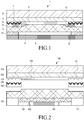
- FIG. 1 is a view illustrating a configuration of a touch panel including a window according to the related art
- the capacitive touch panel 1 includes a window part 2 formed of reinforced glass, a polymer film layer 3 attached to a bottom surface of the window part 2, a pattern ultraviolet (UV) resin layer 4 applied to an lower portion of the polymer film layer 3, a touch sensor film module 5 attached to a bottom surface of the pattern UV resin layer 4, and a display part, e.g., a Liquid Crystal Display (LCD) 6 attached to a bottom surface of the touch sensor film module 5.
- a display part e.g., a Liquid Crystal Display (LCD) 6 attached to a bottom surface of the touch sensor film module 5.
- LCD Liquid Crystal Display
- the pattern UV resin layer 4 is applied to the polymer film layer 3 to form a pattern 7.
- the pattern 7 is formed in the applied pattern UV resin layer 4, and the pattern 7 is deposited 8 and printed 9. Bubbles 12 may be generated during deposition or printing.
- the polymer film layer 3 is attached to the window part 2 by using, e.g., an Optically Clear Adhesive (OCA) (not illustrated).
- OCA Optically Clear Adhesive
- the touch sensor film module 4 is attached to a bracket 6a of the display part (e.g., LCD) 6 through a double-sided tape 10. Then, an air layer 11 is provided between the touch sensor film module 4 and the display part (e.g., LCD) 6 to protect the display part (e.g., LCD) 6 from deflection of the window part 2.
- a bracket 6a of the display part (e.g., LCD) 6 through a double-sided tape 10.
- an air layer 11 is provided between the touch sensor film module 4 and the display part (e.g., LCD) 6 to protect the display part (e.g., LCD) 6 from deflection of the window part 2.
- the configuration of the touch panel is disclosed in Korean patent application Laid-Open No. 10-2011-002857 (issued on January 10, 2011 ).
- the capacitive touch panel according to the related art, light sequentially passes through the media including the window part, the UV resin layer, the touch sensor film module, the air layer, and the display part (e.g., LCD), and thus refractions and reflections of light occur whenever the media are changed, lowering the visibility of the product.
- the display part e.g., LCD
- the UV resin layer is apt to be cracked by a hard primer layer provided in the polymer film layer due to the impact.
- an impact to a side of the touch panel may transfer to the touch panel.
- US2011/033720 A1 relates to a display device with a transparent adhesive sheet in which the occurrence of display unevenness, bubbles and peeling is prevented.
- an aspect of the present invention is to provide a touch panel having improved visibility, that is, in which a transmittance of a product is increased and a visibility of a product is enhanced, by additionally configuring a second ultraviolet (UV) resin layer for preventing refractions and reflections of light in a first UV resin layer, and a method of manufacturing the same.
- UV ultraviolet
- a touch panel having improved visibility includes a window part, at least one ultraviolet (UV) resin layer attached to a bottom surface of the window part, and a display part including a touch sensor film module attached to a bottom surface of the at least one UV resin layer, wherein the UV resin layer prevents refractions and reflections of light.
- UV ultraviolet
- a touch panel having improved visibility includes a window part including a polymer film layer, a first UV resin layer attached to a bottom surface of the polymer film layer, a second UV resin layer attached to a bottom surface of the first UV resin layer to prevent refractions and reflections of light, and a touch sensor film module attached to a bottom surface of the second UV resin layer.
- a method of manufacturing a touch panel having improved visibility includes manufacturing a window part, attaching a polymer film layer to a bottom surface of the window part, attaching a first UV resin layer to a bottom surface of the polymer film layer, attaching a second UV resin layer for preventing refractions and reflections of light to a bottom surface of the first UV resin layer, and attaching a display part including a touch sensor film module to a bottom surface of the second UV resin layer.
- a touch panel having improved visibility includes a window part including a polymer film layer, a first UV resin layer attached to a bottom surface of the polymer film layer, a second UV resin layer attached to a bottom surface of the first UV resin layer to prevent refractions and reflections of light, and a display part including a touch sensor film module attached to a bottom surface of the second UV resin layer, wherein the polymer film layer includes a bonding layer, a film body layer formed on a bottom surface of the bonding layer, and a soft primer layer formed on a bottom surface of the film body layer.
- a touch panel having improved visibility includes a window part including a polymer film layer, a first UV resin layer attached to a bottom surface of the polymer film layer, a second UV resin layer attached to a bottom surface of the first UV resin layer to prevent refractions and reflections of light, and a display part including a touch sensor film module attached to a bottom surface of the second UV resin layer, wherein the polymer film layer and the first UV resin layer are formed to be smaller than the window part and a bracket formed in the display part.
- a method of manufacturing a touch panel having improved visibility includes manufacturing a window part, attaching a polymer film layer to a bottom surface of the window part, attaching a first UV resin layer through a soft primer layer formed in the polymer film layer, attaching a second UV resin layer for preventing refractions and reflections of light to a bottom surface of the first UV resin layer, and attaching a display part including a touch sensor film module to a bottom surface of the second UV resin layer.
- FIG. 3 is a view illustrating a coupled state of the touch panel having improved visibility according to the first exemplary embodiment of the present invention.
- FIG. 4 is an enlarged view illustrating the touch panel having improved visibility according to the first exemplary embodiment of the present invention.
- the touch panel 100 includes a window part 110 including a polymer film layer 120, and a display part 150 including first and second ultraviolet (UV) resin layers 130 and 140 and a touch sensor film module 160.
- the polymer film layer 120 is attached to a bottom surface of the window part 110 so that the first UV resin layer 130 to be described below may be attached to the polymer film layer 120.
- the UV resin layer 130 includes the second UV resin layer 140 to be described below, and is attached to a bottom surface of the polymer film layer 120 to transfer light.
- the second UV resin layer 140 receives light having passed through the first UV resin layer 130, and is attached to a bottom surface of the first UV resin layer 130 to prevent refractions and reflections of the transferred light.
- the touch sensor film module 160 and a bracket 151 formed in the display part 150 are attached to the second UV resin layer 140 together.
- a pattern may be formed in the first UV resin layer.
- the pattern 131 may be one of a decoration pattern, a three-dimensional pattern formed with fine hair lines, and a molding pattern.
- the pattern 131 may be a pattern other than the decoration pattern, the three-dimensional pattern, and the molding pattern (for example, a repeated pattern).
- post-processes such as deposition 170 and printing 180 may be performed on the pattern.
- the post processes may be used to realize a color and a metallic feeling.
- the thickness of the polymer film layer 120 may be between 0.05 mm and 0.15 mm. However, the thickness of the polymer film layer 120 may be less than 0.05 mm or more than 0.15 mm.
- the material of the window part 110 may be one of tempered glass and reinforced plastic.
- the material of the window part 110 may be a material other than tempered glass and reinforced plastic.
- the material of the polymer film layer 120 may be one of Polyethylene Terephthalate (PET), Poly Methyl Methacrylate (PMMA), and Poly Carbonate (PC).
- PET Polyethylene Terephthalate
- PMMA Poly Methyl Methacrylate
- PC Poly Carbonate
- the material of the polymer film layer 120 may be a material other than the above-listed materials.
- the display part 150 may be one of a Liquid Crystal Display (LCD), a Light Emitting Diode (LED), and an Active Matrix Organic Light Emitting Diode (AMOLED).
- the display part may be a display part other than the above-listed display parts.
- the touch sensor film module 160 and the bracket 151 formed in the display part 150 may be attached to the second UV resin layer 140 together.
- the second UV resin layer 140 may be in a liquid state.
- FIG. 4 is an enlarged view illustrating the touch panel having improved visibility according to an exemplary embodiment of the present invention.
- the polymer film layer 120 is attached to a bottom surface of the window part 110 by using an Optical Clean Adhesive (OCA) (not illustrated).
- OCA Optical Clean Adhesive
- the first UV resin layer 130 is formed on a bottom surface of the polymer film layer 120, and a pattern is formed in the first UV resin layer 130.
- the pattern 131 is a decoration pattern, and the decoration pattern is a repeated design pattern including fine hair lines.
- Post-processes such as deposition 170 and printing 180 are performed on the pattern 131 to realize a color and a metallic feeling.
- the second UV resin layer 140 in a liquid state is formed on a bottom surface of the first UV resin layer 130.
- the touch sensor film module 160 and the bracket of the display part 150 are attached to the second UV resin together.
- light is introduced into the window part 110, and the introduced light passes through the polymer film layer 120. Then, light is refracted and reflected whenever the light passes through the window part 110 and the polymer film layer 120.
- the light having passed through the polymer film layer 120 is introduced into the first UV resin layer 130 and is refracted and reflected at the same time.
- the light having passed through the first UV resin layer 130 passes the second UV resin layer 140 of the same kind, which prevents refractions and reflections.
- the light is refracted and reflected when passing through the first UV resin layer 130, and is introduced into the second UV resin layer 140 as it is.
- the introduced light passes through the second UV resin layer 140 as it is, and not being refracted and reflected.
- the second UV resin layer 140 passes the light without refracting and reflecting it, and the light is then transferred to the display part 150 after passing through the touch sensor film module 160.
- the second UV resin layer 140 for additionally preventing refractions and reflections of light in the first UV resin layer 130, the visibility of a product can be enhanced, the clarity of the product can be enhanced, and the design of the product can become more appealing.
- the second UV resin layer 140 in a liquid state by applying the second UV resin layer 140 in a liquid state to the first UV hardening resin layer 130 having a pattern 130, a space formed by a pattern according to the related art can be prevented and bubbles 12 (see FIG. 1 ) generated in the space are prevented.
- the defect rate of the product due to the bubbles generated can be reduced.
- bracket of the display part 150 and the touch sensor film module 160 are attached to each other by using a double-sided tape 10 (see FIG. 1 ) to form an air layer in the related art, the attached area of the double-sided tape is so small that the display part 150 and the touch sensor film module 160 can be easily separated from each other.
- the attached area may be made wider so that the touch sensor film module 160 and the display part 150 can be attached to each other so as to enhance an attaching force of the product.
- Touch panel 10 (see FIG. 2 ), according to an exemplary embodiment of the present invention, is applicable to an electronic device (not illustrated).
- the present invention is not necessarily limited to electronic devices and may be applied to various types of electronic devices.
- Examples of various types of electronic devices may include all information communication devices and multimedia devices such as an MP3 player, a Portable Multimedia Player (PMP), a navigation system, a gaming device, a laptop computer, an advertising panel, a television (TV), a digital broadcasting player, a Personal Digital Assistant (PDA), and a smart phone, and application devices thereof, including all mobile communication terminals operated based on communication protocols corresponding to various communication systems.
- MP3 player a Portable Multimedia Player
- PMP Portable Multimedia Player
- gaming device Portable Multimedia Player
- laptop computer an advertising panel
- TV television
- PDA Personal Digital Assistant
- smart phone and application devices thereof, including all mobile communication terminals operated based on communication protocols corresponding to various communication systems.
- FIG. 5 is a view illustrating a method of manufacturing the touch panel having improved visibility according to an exemplary embodiment of the present invention.
- step S1 the window part 110 formed of tempered glass is manufactured.
- step S2 the polymer film layer 120 is attached to a bottom surface of the window part 110 manufactured in step S1 by using an Optical Clean Adhesive (OCA) (not illustrated).
- OCA Optical Clean Adhesive
- step S3 the first UV resin layer 130 is attached to a bottom surface of the polymer film layer 120 from step S2.
- the decoration pattern 131 is formed in the first UV resin layer 130, and the decoration pattern 131 is processed through deposition 170 and printing 180.
- step S4 the second UV resin layer 140 for preventing refractions and reflections of light is attached to a bottom surface of the first UV resin layer 130 from step S3.
- step S5 the display part 150 including the touch sensor film module 160 is attached to a bottom surface of the second UV resin layer 140 from step S4.
- the first UV resin layer 130 corresponds to a pattern UV resin layer for forming a pattern
- the second UV resin layer 140 corresponds to an attaching UV resin layer for attaching the touch sensor film module 160 and the display part 150 together.
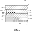
- FIG. 6 is a view illustrating a coupled state of a touch panel having improved visibility according to a second exemplary embodiment of the present invention.
- FIG. 7 is an enlarged view illustrating a polymer film layer of the touch panel having improved visibility according to the second exemplary embodiment of the present invention.
- the touch panel 200 includes a window part 210 including a polymer film layer 220, a display part 250 including first and second UV resin layers 230 and 240 and a touch sensor film module 260.
- the polymer film layer 220 is attached to a bottom surface of the window part 210 so that the first UV resin layer 230 to be described below may be attached to the polymer film layer 220.
- the first UV resin layer 230 includes the second UV resin layer 240 to be described below, and is attached to a bottom surface of the polymer film layer 220 to transfer light.
- the second UV resin layer 240 receives light having passed through the first UV resin layer 230, and is attached to a bottom surface of the first UV resin layer 230 to prevent refractions and reflections of the transferred light.
- the touch sensor film module 260 is attached to a bottom of the second UV resin layer 240.
- the touch panel 200 by additionally configuring the second UV resin layer 240, refractions and reflections of light caused by use of the first UV resin layer 230, and lowering of the screen quality of the display part 250 due to distortion of a surface of the first UV resin layer 230 and scratches, can be prevented.
- a pattern 270 may be formed in the first UV resin layer 230.
- a bracket 251 formed in the display part 250 is attached to a bottom surface of the pattern 270 by using a double-sided tape 280.
- the pattern 270 may be any one of a decoration pattern, a three-dimensional pattern formed with hair lines, a molding pattern, or a lattice pattern.
- the pattern 270 may also be a pattern other than the disclosed patterns (for example, a repeated pattern).
- post-processes such as deposition 271 and printing 272 may be performed on the pattern 270.
- the post processes may be used to realize a color and a metallic feeling, wherein the pattern 270 may be realized on a bottom surface of the polymer film layer 220 through a roller or stamp process.
- the polymer film layer 220 may include a bonding layer 220a, a film body layer 220b, and a soft primer layer 220c.
- the bonding layer 220a is formed of an OCA, and the polymer 220 is attached to a bottom surface of the window part 210 by using the optical clear adhesive.
- the film body layer 220b is formed on a bottom surface of the bonding layer 220a.
- the soft primer layer 220c is formed on a bottom surface of the film body layer 220b to increase a bonding force with the first UV resin layer 230 and an impact-resistant property.
- a thickness of the bonding layer 220a may be 25 ⁇ m to 50 ⁇ m. However, a thickness of the bonding layer 220a may be less than 25 ⁇ m or more than 50 ⁇ m.
- a material of the film body layer 220b may be any one of PET, PMMA, and PC. However, the material of the polymer film layer 220 may also be a material other than the above-listed materials.
- the primer layer 220c may correspond to a single-layered or multilayered primer layer to increase a bonding force with the first UV resin layer 230 and to add an impact-resistant property.
- a hardness of the primer layer 220c may be a pencil hardness of H to B to prevent the first UV resin layer 230 from cracking when an electronic device is dropped.
- the polymer film layer 220 may be bonded to the window part 210 through a roller or stamp process.
- An upper surface of the window part 210 may correspond to a plane or a shape having a curvature. That is, an upper surface of the window part 210 may be any one of 2.5 D and 3D shapes having a curvature.
- the first and second UV resin layers 230 and 240 may be formed of an acrylate or polyurethane material. However, the first and second UV resin layers 230 and 240 may also be a material other than the disclosed materials. A hardness of the first and second resin layers 230 and 240 may be a pencil hardness of F to B.
- the polymer film layer 220 and the first UV resin layer 230 may be formed to be smaller than the window part 210 and the bracket 251 formed in the display part 250.
- a thickness of the avoidance space 300 may be from 0 to 0.3 mm, or more specifically, a thickness of the avoidance space 300 may be from only 0 mm to 0.25 mm.
- the window part 210 is attached to the bonding layer 220a formed of an OCA (not illustrated) formed on an upper surface of the polymer film layer 220.
- the first UV resin layer 230 is attached by using the soft primer layer 220c formed on a bottom surface of the polymer film layer 220.
- the pattern 270 is formed in the first UV resin layer 230.
- the pattern may correspond to any of a pattern of a hair line, a lattice pattern, and the like.
- the second UV resin layer 240 is attached to a bottom surface of the first UV resin layer 230.
- the touch sensor film module 260 is attached to the second UV resin layer 240, and the bracket 251 of the display part 250 is attached to the pattern 270 by using a double-sided tape 280.
- the polymer film layer 220 and the first UV resin layer 230 are formed to be smaller than the window part 210 and the bracket 251 of the display part 250, and thus the polymer film layer 220 and the first UV resin layer 230 are formed between the window part 210 and the bracket 251 of the display part 250 are recessed by a predetermined depth to inner sides of the window part 210 and the bracket 251 of the display part 250 at the same time.
- the polymer film layer 220 and the first UV resin layer 230 are recessed and the avoidance space 300 is formed between the window part 210 and the bracket 251, and an impact F (see FIG. 7 ) transferred to side surfaces of the polymer film layer 200 and the first UV resin layer 230 can be avoided by the avoidance space 300 when the touch panel 200 drops.
- the protruding window part 210 and bracket 251 are brought into contact so that an impact F is applied to the protruding window part 210 and bracket 251 and the mitigated impact F is transferred to the polymer film layer 220 and the first UV resin layer 230.
- the window part 210 and the bracket 251 first contact the external coupling structure so that an impact is applied to the window part 210 and the bracket 251 and the mitigated impact is transferred to the polymer film layer 220 and the first UV resin layer 230.
- the polymer film layer 220 and the first UV resin layer 230 are first directly brought into contact when the touch panel 200 is dropped, and an external coupling structure is pushed in to prevent an impact F (see FIG. 7 ) from being transferred. Accordingly, the polymer film layer 220 and the first UV resin layer 230 can be protected.
- the primer layer (not illustrated) formed on an existing polymer film layer 3 may be formed of a hard material, causing the UV resin layer 4 (see FIG. 1 ) to easily crack when an electronic device is dropped.
- a soft primer layer may be formed in the polymer film layer 220 to improve a bonding force of the first UV resin layer 230 and to prevent the first UV resin layer 230 from cracking due to an impact F (see FIG. 7 ) generated if, for example, an electronic device is dropped.
- FIG. 8 is a view illustrating the method of manufacturing a touch panel having improved visibility according to an exemplary embodiment of the present invention.
- step S1 the window part 210 formed of tempered glass is manufactured.
- step S2 the polymer film layer 220 is attached to a bottom surface of the window part 210 manufactured in step S1 by using the bonding layer 220a.
- step S3 the first UV resin layer 230 is attached to a bottom surface of the polymer film layer 220 by using the soft primer layer 220c from step S2.
- a pattern 270 such as a hair line, a lattice pattern, or the like may be formed in the first UV resin layer 230
- step S4 the second UV resin layer 240 for preventing refractions and reflections of light is attached to a bottom surface of the first UV resin layer 230 from step S3.
- step S5 the display part 250 including the touch sensor film module 260 is attached to a bottom surface of the second UV resin layer 240 from step S4.
- the polymer film layer 220 and the first UV resin layer 230 are formed to be smaller than the window part 210 and the bracket 251 formed in the display part 250.
- a thickness of the avoidance space 300 may be from 0 to 0.3 mm, or more specifically, a thickness of the avoidance space 300 may be from only 0 to 0.25 mm.
Landscapes
- Engineering & Computer Science (AREA)
- General Engineering & Computer Science (AREA)
- Theoretical Computer Science (AREA)
- Human Computer Interaction (AREA)
- Physics & Mathematics (AREA)
- General Physics & Mathematics (AREA)
- Microelectronics & Electronic Packaging (AREA)
- Position Input By Displaying (AREA)
- Laminated Bodies (AREA)
Description
- The present invention relates to a touch panel. More particularly, the present invention relates to a touch panel having improved visibility, and a method of manufacturing the same.
- In general, the visibility of portable communication devices has improved due to remarkable developments in multimedia and display technologies. Accordingly, touch panels are increasingly employed in portable communication devices.
- In the case of a general resistive touch sensor, since the touch panel can provide location information only when two sensors contact each other as a result of touch pressure, a film needs to be attached to a window provided in a portable communication device. In contrast, a capacitive touch panel provides the location of a point where electric charges are discharged during a touch.
- A capacitive touch panel will be described in more detail as follows.
-
FIG. 1 is a view illustrating a configuration of a touch panel including a window according to the related art - Referring to
FIG. 1 , thecapacitive touch panel 1 includes awindow part 2 formed of reinforced glass, apolymer film layer 3 attached to a bottom surface of thewindow part 2, a pattern ultraviolet (UV)resin layer 4 applied to an lower portion of thepolymer film layer 3, a touchsensor film module 5 attached to a bottom surface of the patternUV resin layer 4, and a display part, e.g., a Liquid Crystal Display (LCD) 6 attached to a bottom surface of the touchsensor film module 5. - The pattern
UV resin layer 4 is applied to thepolymer film layer 3 to form apattern 7. Thepattern 7 is formed in the applied patternUV resin layer 4, and thepattern 7 is deposited 8 and printed 9.Bubbles 12 may be generated during deposition or printing. Thepolymer film layer 3 is attached to thewindow part 2 by using, e.g., an Optically Clear Adhesive (OCA) (not illustrated). - In
FIG. 1 , the touchsensor film module 4 is attached to a bracket 6a of the display part (e.g., LCD) 6 through a double-sided tape 10. Then, anair layer 11 is provided between the touchsensor film module 4 and the display part (e.g., LCD) 6 to protect the display part (e.g., LCD) 6 from deflection of thewindow part 2. - The configuration of the touch panel is disclosed in Korean patent application Laid-Open No.
10-2011-002857 (issued on January 10, 2011 - However, when light passes through different media, refractions and reflections generally occur in the touch panel due to differences in the refractivity of the different media.
- Thus, in the capacitive touch panel according to the related art, light sequentially passes through the media including the window part, the UV resin layer, the touch sensor film module, the air layer, and the display part (e.g., LCD), and thus refractions and reflections of light occur whenever the media are changed, lowering the visibility of the product.
- In addition to the above problems in the related art, if an existing touch panel is dropped, the UV resin layer is apt to be cracked by a hard primer layer provided in the polymer film layer due to the impact. Also, in the related art, an impact to a side of the touch panel may transfer to the touch panel.
- Therefore, a need exists for a method and apparatus for adding another UV resin layer for minimizing refractions and reflections of light to the existing resin layer. Additionally, a need exists for a soft primer layer to prevent the UV resin layer from being cracked due to the impact of, e.g., the touch panel being dropped. A further need also exists for a space to be provided in order to avoid damage from an impact to a side surface of the touch panel.
- The above information is presented as background information only to assist with an understanding of the present disclosure. No determination has been made, and no assertion is made, as to whether any of the above might be applicable as prior art with regard to the present invention.
US2011/033720 A1 relates to a display device with a transparent adhesive sheet in which the occurrence of display unevenness, bubbles and peeling is prevented. - Aspects of the present invention are to address at least the above-mentioned problems and/or disadvantages and to provide at least the advantages described below. Accordingly, an aspect of the present invention is to provide a touch panel having improved visibility, that is, in which a transmittance of a product is increased and a visibility of a product is enhanced, by additionally configuring a second ultraviolet (UV) resin layer for preventing refractions and reflections of light in a first UV resin layer, and a method of manufacturing the same.
- In accordance with an aspect of the present invention, a touch panel having improved visibility is provided. The touch panel includes a window part, at least one ultraviolet (UV) resin layer attached to a bottom surface of the window part, and a display part including a touch sensor film module attached to a bottom surface of the at least one UV resin layer, wherein the UV resin layer prevents refractions and reflections of light.
- In accordance with another aspect of the present invention, a touch panel having improved visibility is provided. The touch panel includes a window part including a polymer film layer, a first UV resin layer attached to a bottom surface of the polymer film layer, a second UV resin layer attached to a bottom surface of the first UV resin layer to prevent refractions and reflections of light, and a touch sensor film module attached to a bottom surface of the second UV resin layer.
- In accordance with another aspect of the present invention, a method of manufacturing a touch panel having improved visibility is provided. The method includes manufacturing a window part, attaching a polymer film layer to a bottom surface of the window part, attaching a first UV resin layer to a bottom surface of the polymer film layer, attaching a second UV resin layer for preventing refractions and reflections of light to a bottom surface of the first UV resin layer, and attaching a display part including a touch sensor film module to a bottom surface of the second UV resin layer.
- In accordance with another aspect of the present invention, a touch panel having improved visibility is provided. The touch panel includes a window part including a polymer film layer, a first UV resin layer attached to a bottom surface of the polymer film layer, a second UV resin layer attached to a bottom surface of the first UV resin layer to prevent refractions and reflections of light, and a display part including a touch sensor film module attached to a bottom surface of the second UV resin layer, wherein the polymer film layer includes a bonding layer, a film body layer formed on a bottom surface of the bonding layer, and a soft primer layer formed on a bottom surface of the film body layer.
- In accordance with another aspect of the present invention, a touch panel having improved visibility is provided. The touch panel includes a window part including a polymer film layer, a first UV resin layer attached to a bottom surface of the polymer film layer, a second UV resin layer attached to a bottom surface of the first UV resin layer to prevent refractions and reflections of light, and a display part including a touch sensor film module attached to a bottom surface of the second UV resin layer, wherein the polymer film layer and the first UV resin layer are formed to be smaller than the window part and a bracket formed in the display part.
- In accordance with another aspect of the present invention, a method of manufacturing a touch panel having improved visibility is provided. The method includes manufacturing a window part, attaching a polymer film layer to a bottom surface of the window part, attaching a first UV resin layer through a soft primer layer formed in the polymer film layer, attaching a second UV resin layer for preventing refractions and reflections of light to a bottom surface of the first UV resin layer, and attaching a display part including a touch sensor film module to a bottom surface of the second UV resin layer.
- Other aspects, advantages, and salient features of the invention will become apparent to those skilled in the art from the following detailed description, which, taken in conjunction with the annexed drawings, discloses exemplary embodiments of the invention. The invention will be carried out according to the attached independent claims.
- The above and other aspects, features, and advantages of the present invention will be more apparent from the following description taken in conjunction with the accompanying drawings, in which:
-
FIG. 1 is a view illustrating a configuration of a touch panel including a window according to the related art; -
FIG. 2 is an exploded view illustrating a touch panel having improved visibility according to a first exemplary embodiment of the present invention; -
FIG. 3 is a view illustrating a coupled state of the touch panel having improved visibility according to the first exemplary embodiment of the present invention; -
FIG. 4 is an enlarged view illustrating the touch panel having improved visibility according to the first exemplary embodiment of the present invention; -
FIG. 5 is a flowchart illustrating a method of manufacturing a touch panel having improved visibility according to the first exemplary embodiment of the present invention; -
FIG. 6 is a view illustrating a coupled state of a touch panel having improved visibility according to a second exemplary embodiment of the present invention; -
FIG. 7 is an enlarged view illustrating a polymer film layer of the touch panel having improved visibility according to the second exemplary embodiment of the present invention; and -
FIG. 8 is a flowchart illustrating a method of manufacturing a touch panel having improved visibility according to the second exemplary embodiment of the present invention. - Throughout the drawings, it should be noted that like reference numbers are used to depict the same or similar elements, features, and structures.
- The following description with reference to the accompanying drawings is provided to assist in a comprehensive understanding of exemplary embodiments of the invention as defined by the claims and their equivalents. It includes various specific details to assist in that understanding but these are to be regarded as merely exemplary. Accordingly, those of ordinary skill in the art will recognize that various changes and modifications of the embodiments described herein can be made without departing from the scope and spirit of the invention. In addition, descriptions of well-known functions and constructions may be omitted for clarity and conciseness.
- The terms and words used in the following description and claims are not limited to the bibliographical meanings, but, are merely used by the inventor to enable a clear and consistent understanding of the invention. Accordingly, it should be apparent to those skilled in the art that the following description of exemplary embodiments of the present invention is provided for illustration purpose only and not for the purpose of limiting the invention as defined by the appended claims and their equivalents.
- It is to be understood that the singular forms "a," "an," and "the" include plural referents unless the context clearly dictates otherwise. Thus, for example, reference to "a component surface" includes reference to one or more of such surfaces.
-
FIG. 3 is a view illustrating a coupled state of the touch panel having improved visibility according to the first exemplary embodiment of the present invention.FIG. 4 is an enlarged view illustrating the touch panel having improved visibility according to the first exemplary embodiment of the present invention. - Referring to
FIGs. 2 and3 , thetouch panel 100 includes awindow part 110 including apolymer film layer 120, and adisplay part 150 including first and second ultraviolet (UV) resin layers 130 and 140 and a touchsensor film module 160. Thepolymer film layer 120 is attached to a bottom surface of thewindow part 110 so that the firstUV resin layer 130 to be described below may be attached to thepolymer film layer 120. TheUV resin layer 130 includes the secondUV resin layer 140 to be described below, and is attached to a bottom surface of thepolymer film layer 120 to transfer light. The secondUV resin layer 140 receives light having passed through the firstUV resin layer 130, and is attached to a bottom surface of the firstUV resin layer 130 to prevent refractions and reflections of the transferred light. The touchsensor film module 160 and abracket 151 formed in thedisplay part 150 are attached to the secondUV resin layer 140 together. - Further referring to
FIG. 2 , a pattern may be formed in the first UV resin layer. Thepattern 131 may be one of a decoration pattern, a three-dimensional pattern formed with fine hair lines, and a molding pattern. Here, thepattern 131 may be a pattern other than the decoration pattern, the three-dimensional pattern, and the molding pattern (for example, a repeated pattern). - In addition, post-processes such as
deposition 170 andprinting 180 may be performed on the pattern. In an exemplary implementation, the post processes may be used to realize a color and a metallic feeling. - In exemplary embodiments, the thickness of the
polymer film layer 120 may be between 0.05 mm and 0.15 mm. However, the thickness of thepolymer film layer 120 may be less than 0.05 mm or more than 0.15 mm. - In exemplary embodiments, the material of the
window part 110 may be one of tempered glass and reinforced plastic. However, the material of thewindow part 110 may be a material other than tempered glass and reinforced plastic. - In exemplary embodiments, the material of the
polymer film layer 120 may be one of Polyethylene Terephthalate (PET), Poly Methyl Methacrylate (PMMA), and Poly Carbonate (PC). However, the material of thepolymer film layer 120 may be a material other than the above-listed materials. - In exemplary embodiments, the
display part 150 may be one of a Liquid Crystal Display (LCD), a Light Emitting Diode (LED), and an Active Matrix Organic Light Emitting Diode (AMOLED). However, the display part may be a display part other than the above-listed display parts. - Further referring to
FIG. 3 , in describing the secondUV resin layer 140 in more detail, as illustrated inFIG. 3 , the touchsensor film module 160 and thebracket 151 formed in thedisplay part 150 may be attached to the secondUV resin layer 140 together. - Here, the second
UV resin layer 140 may be in a liquid state. -
FIG. 4 is an enlarged view illustrating the touch panel having improved visibility according to an exemplary embodiment of the present invention. - Referring to
FIG. 4 , thepolymer film layer 120 is attached to a bottom surface of thewindow part 110 by using an Optical Clean Adhesive (OCA) (not illustrated). The firstUV resin layer 130 is formed on a bottom surface of thepolymer film layer 120, and a pattern is formed in the firstUV resin layer 130. Thepattern 131 is a decoration pattern, and the decoration pattern is a repeated design pattern including fine hair lines. Post-processes such asdeposition 170 andprinting 180 are performed on thepattern 131 to realize a color and a metallic feeling. In this state, the secondUV resin layer 140 in a liquid state is formed on a bottom surface of the firstUV resin layer 130. - The touch
sensor film module 160 and the bracket of thedisplay part 150 are attached to the second UV resin together. - Further referring to
FIG. 4 , light is introduced into thewindow part 110, and the introduced light passes through thepolymer film layer 120. Then, light is refracted and reflected whenever the light passes through thewindow part 110 and thepolymer film layer 120. - The light having passed through the
polymer film layer 120 is introduced into the firstUV resin layer 130 and is refracted and reflected at the same time. - The light having passed through the first
UV resin layer 130 passes the secondUV resin layer 140 of the same kind, which prevents refractions and reflections. - That is, the light is refracted and reflected when passing through the first
UV resin layer 130, and is introduced into the secondUV resin layer 140 as it is. The introduced light passes through the secondUV resin layer 140 as it is, and not being refracted and reflected. The secondUV resin layer 140 passes the light without refracting and reflecting it, and the light is then transferred to thedisplay part 150 after passing through the touchsensor film module 160. - Since the light having passed the first
UV resin layer 130 passes the secondUV resin layer 140 as it is and not being refracted and reflected, screen visibility can be improved, and screen degradation of thedisplay part 150 due to a reduction in the transmittance of light can be addressed at the same time. - That is, by configuring the second
UV resin layer 140 for additionally preventing refractions and reflections of light in the firstUV resin layer 130, the visibility of a product can be enhanced, the clarity of the product can be enhanced, and the design of the product can become more appealing. - According to the related art, when a film-type touch sensor film module is attached to a bottom surface of a UV resin layer having a pattern, an attached space is formed between the pattern and the touch sensor film module, and bubbles 12 (see
FIG. 1 ) are generated in the space. Accordingly, a defect rate of the product increases. - Thus, in order to address these disadvantages, by applying the second
UV resin layer 140 in a liquid state to the first UV hardeningresin layer 130 having apattern 130, a space formed by a pattern according to the related art can be prevented and bubbles 12 (seeFIG. 1 ) generated in the space are prevented. Thus, the defect rate of the product due to the bubbles generated can be reduced. - In addition, although the bracket of the
display part 150 and the touchsensor film module 160 are attached to each other by using a double-sided tape 10 (seeFIG. 1 ) to form an air layer in the related art, the attached area of the double-sided tape is so small that thedisplay part 150 and the touchsensor film module 160 can be easily separated from each other. - Thus, in order to address the disadvantages, in the second
UV resin layer 140, the attached area may be made wider so that the touchsensor film module 160 and thedisplay part 150 can be attached to each other so as to enhance an attaching force of the product. - Touch panel 10 (see
FIG. 2 ), according to an exemplary embodiment of the present invention, is applicable to an electronic device (not illustrated). However, the present invention is not necessarily limited to electronic devices and may be applied to various types of electronic devices. - Examples of various types of electronic devices according to exemplary embodiments of the present invention may include all information communication devices and multimedia devices such as an MP3 player, a Portable Multimedia Player (PMP), a navigation system, a gaming device, a laptop computer, an advertising panel, a television (TV), a digital broadcasting player, a Personal Digital Assistant (PDA), and a smart phone, and application devices thereof, including all mobile communication terminals operated based on communication protocols corresponding to various communication systems.
- Hereinafter, a method of manufacturing the touch panel having improved visibility according to an exemplary embodiment of the present invention will be described in detail.
-
FIG. 5 is a view illustrating a method of manufacturing the touch panel having improved visibility according to an exemplary embodiment of the present invention. - Referring to
FIG. 5 , a method of manufacturing thetouch panel 100 having improved visibility will be described. In step S1, thewindow part 110 formed of tempered glass is manufactured. - In step S2, the
polymer film layer 120 is attached to a bottom surface of thewindow part 110 manufactured in step S1 by using an Optical Clean Adhesive (OCA) (not illustrated). - In step S3, the first
UV resin layer 130 is attached to a bottom surface of thepolymer film layer 120 from step S2. - The
decoration pattern 131 is formed in the firstUV resin layer 130, and thedecoration pattern 131 is processed throughdeposition 170 andprinting 180. - In step S4, the second
UV resin layer 140 for preventing refractions and reflections of light is attached to a bottom surface of the firstUV resin layer 130 from step S3. - In step S5, the
display part 150 including the touchsensor film module 160 is attached to a bottom surface of the secondUV resin layer 140 from step S4. - The first
UV resin layer 130 corresponds to a pattern UV resin layer for forming a pattern, and the secondUV resin layer 140 corresponds to an attaching UV resin layer for attaching the touchsensor film module 160 and thedisplay part 150 together. -
FIG. 6 is a view illustrating a coupled state of a touch panel having improved visibility according to a second exemplary embodiment of the present invention.FIG. 7 is an enlarged view illustrating a polymer film layer of the touch panel having improved visibility according to the second exemplary embodiment of the present invention. - Referring to
FIGs. 6 and7 , thetouch panel 200 includes awindow part 210 including apolymer film layer 220, adisplay part 250 including first and second UV resin layers 230 and 240 and a touchsensor film module 260. Thepolymer film layer 220 is attached to a bottom surface of thewindow part 210 so that the firstUV resin layer 230 to be described below may be attached to thepolymer film layer 220. The firstUV resin layer 230 includes the secondUV resin layer 240 to be described below, and is attached to a bottom surface of thepolymer film layer 220 to transfer light. The secondUV resin layer 240 receives light having passed through the firstUV resin layer 230, and is attached to a bottom surface of the firstUV resin layer 230 to prevent refractions and reflections of the transferred light. The touchsensor film module 260 is attached to a bottom of the secondUV resin layer 240. - In the
touch panel 200, by additionally configuring the secondUV resin layer 240, refractions and reflections of light caused by use of the firstUV resin layer 230, and lowering of the screen quality of thedisplay part 250 due to distortion of a surface of the firstUV resin layer 230 and scratches, can be prevented. - A
pattern 270 may be formed in the firstUV resin layer 230. Abracket 251 formed in thedisplay part 250 is attached to a bottom surface of thepattern 270 by using a double-sided tape 280. - The
pattern 270 may be any one of a decoration pattern, a three-dimensional pattern formed with hair lines, a molding pattern, or a lattice pattern. Thepattern 270 may also be a pattern other than the disclosed patterns (for example, a repeated pattern). - In addition, post-processes such as deposition 271 and
printing 272 may be performed on thepattern 270. In an exemplary implementation, the post processes may be used to realize a color and a metallic feeling, wherein thepattern 270 may be realized on a bottom surface of thepolymer film layer 220 through a roller or stamp process. - In describing the
polymer film layer 220 with reference toFIG. 7 in more detail, thepolymer film layer 220 may include abonding layer 220a, afilm body layer 220b, and asoft primer layer 220c. Thebonding layer 220a is formed of an OCA, and thepolymer 220 is attached to a bottom surface of thewindow part 210 by using the optical clear adhesive. Thefilm body layer 220b is formed on a bottom surface of thebonding layer 220a. Thesoft primer layer 220c is formed on a bottom surface of thefilm body layer 220b to increase a bonding force with the firstUV resin layer 230 and an impact-resistant property. - In exemplary embodiments, a thickness of the
bonding layer 220a may be 25 µm to 50 µm. However, a thickness of thebonding layer 220a may be less than 25 µm or more than 50 µm. - A material of the
film body layer 220b may be any one of PET, PMMA, and PC. However, the material of thepolymer film layer 220 may also be a material other than the above-listed materials. - The
primer layer 220c may correspond to a single-layered or multilayered primer layer to increase a bonding force with the firstUV resin layer 230 and to add an impact-resistant property. - A hardness of the
primer layer 220c may be a pencil hardness of H to B to prevent the firstUV resin layer 230 from cracking when an electronic device is dropped. - The
polymer film layer 220 may be bonded to thewindow part 210 through a roller or stamp process. - An upper surface of the
window part 210 may correspond to a plane or a shape having a curvature. That is, an upper surface of thewindow part 210 may be any one of 2.5 D and 3D shapes having a curvature. - The first and second UV resin layers 230 and 240 may be formed of an acrylate or polyurethane material. However, the first and second UV resin layers 230 and 240 may also be a material other than the disclosed materials. A hardness of the first and second resin layers 230 and 240 may be a pencil hardness of F to B.
- As illustrated in
FIG. 6 , thepolymer film layer 220 and the firstUV resin layer 230 may be formed to be smaller than thewindow part 210 and thebracket 251 formed in thedisplay part 250. - That is, an
avoidance space 300 for avoiding an impact F (seeFIG. 7 ) transferred to a side of the electronic device if, for example, the electronic device (not illustrated) is dropped, or for preventing an external coupling structure from being impacted when the coupling structure is pushed in, is formed between thepolymer film layer 220 and thebracket 251. - In exemplary embodiments, a thickness of the
avoidance space 300 may be from 0 to 0.3 mm, or more specifically, a thickness of theavoidance space 300 may be from only 0 mm to 0.25 mm. - In describing a process of manufacturing the
touch panel 200 having improved visibility in more detail with reference toFIGs. 6 and7 , as illustrated inFIG. 6 , thewindow part 210 is attached to thebonding layer 220a formed of an OCA (not illustrated) formed on an upper surface of thepolymer film layer 220. The firstUV resin layer 230 is attached by using thesoft primer layer 220c formed on a bottom surface of thepolymer film layer 220. Thepattern 270 is formed in the firstUV resin layer 230. The pattern may correspond to any of a pattern of a hair line, a lattice pattern, and the like. In this state, the secondUV resin layer 240 is attached to a bottom surface of the firstUV resin layer 230. The touchsensor film module 260 is attached to the secondUV resin layer 240, and thebracket 251 of thedisplay part 250 is attached to thepattern 270 by using a double-sided tape 280. - Referring to
FIG. 7 , thepolymer film layer 220 and the firstUV resin layer 230 are formed to be smaller than thewindow part 210 and thebracket 251 of thedisplay part 250, and thus thepolymer film layer 220 and the firstUV resin layer 230 are formed between thewindow part 210 and thebracket 251 of thedisplay part 250 are recessed by a predetermined depth to inner sides of thewindow part 210 and thebracket 251 of thedisplay part 250 at the same time. - That is, the
polymer film layer 220 and the firstUV resin layer 230 are recessed and theavoidance space 300 is formed between thewindow part 210 and thebracket 251, and an impact F (seeFIG. 7 ) transferred to side surfaces of thepolymer film layer 200 and the firstUV resin layer 230 can be avoided by theavoidance space 300 when thetouch panel 200 drops. - Referring to
FIG. 7 , when thetouch panel 200 is dropped, the protrudingwindow part 210 andbracket 251 are brought into contact so that an impact F is applied to the protrudingwindow part 210 andbracket 251 and the mitigated impact F is transferred to thepolymer film layer 220 and the firstUV resin layer 230. - Further, if, for example, an external coupling structure (not illustrated) is pushed into the
touch panel 200, thewindow part 210 and thebracket 251 first contact the external coupling structure so that an impact is applied to thewindow part 210 and thebracket 251 and the mitigated impact is transferred to thepolymer film layer 220 and the firstUV resin layer 230. - Thus, the
polymer film layer 220 and the firstUV resin layer 230 are first directly brought into contact when thetouch panel 200 is dropped, and an external coupling structure is pushed in to prevent an impact F (seeFIG. 7 ) from being transferred. Accordingly, thepolymer film layer 220 and the firstUV resin layer 230 can be protected. - Additionally, the primer layer (not illustrated) formed on an existing polymer film layer 3 (see
FIG. 1 ) may be formed of a hard material, causing the UV resin layer 4 (seeFIG. 1 ) to easily crack when an electronic device is dropped. - Thus, in order to address this disadvantage, in exemplary embodiments of the present invention, a soft primer layer may be formed in the
polymer film layer 220 to improve a bonding force of the firstUV resin layer 230 and to prevent the firstUV resin layer 230 from cracking due to an impact F (seeFIG. 7 ) generated if, for example, an electronic device is dropped. - Hereinafter, a method of manufacturing the touch panel having improved visibility according to the second embodiment of the present invention will be described in detail.
-
FIG. 8 is a view illustrating the method of manufacturing a touch panel having improved visibility according to an exemplary embodiment of the present invention. - Referring to
FIG. 8 , the method of manufacturing thetouch panel 200 having improved visibility will be described. In step S1, thewindow part 210 formed of tempered glass is manufactured. - In step S2, the
polymer film layer 220 is attached to a bottom surface of thewindow part 210 manufactured in step S1 by using thebonding layer 220a. - In step S3, the first
UV resin layer 230 is attached to a bottom surface of thepolymer film layer 220 by using thesoft primer layer 220c from step S2. - A
pattern 270 such as a hair line, a lattice pattern, or the like may be formed in the firstUV resin layer 230 - In step S4, the second
UV resin layer 240 for preventing refractions and reflections of light is attached to a bottom surface of the firstUV resin layer 230 from step S3. - In step S5, the
display part 250 including the touchsensor film module 260 is attached to a bottom surface of the secondUV resin layer 240 from step S4. - The
polymer film layer 220 and the firstUV resin layer 230 are formed to be smaller than thewindow part 210 and thebracket 251 formed in thedisplay part 250. - That is, an
avoidance space 300 for avoiding an impact transferred to a side of the electronic device if, for example, the electronic device (not illustrated) is dropped, or for preventing an external coupling structure from being impacted when the coupling structure (not illustrated) is pushed in, is formed between thepolymer film layer 220 and thebracket 251. - In exemplary embodiments of the present invention, a thickness of the
avoidance space 300 may be from 0 to 0.3 mm, or more specifically, a thickness of theavoidance space 300 may be from only 0 to 0.25 mm.
Claims (14)
- A touch panel having improved visibility, the touch panel comprising:a window part (110) including a polymer film layer (120);a first ultraviolet, UV, resin layer (130) attached to a bottom surface of the polymer film layer;a second UV resin layer (140) attached to a bottom surface of the first UV resin layer to prevent refractions and reflections of light; anda display part (150) including a touch sensor film module (160) attached to a bottom surface of the second UV resin layer,wherein the polymer film layer comprises:a bonding layer (220a);a film body layer (220b) formed on a bottom surface of the bonding layer; anda soft primer layer (220c) formed on a bottom surface of the film body layer.
- The touch panel of claim 1, wherein a thickness of the bonding layer is from 25 µm to 50 µm.
- The touch panel of claim 1, wherein a material of the film body layer comprises at least one of Polyethylene Terephthalate, PET, Poly Methyl Methacrylate, PMMA, and Poly Carbonate, PC.
- The touch panel of claim 1, wherein the primer layer is a single-layered or a multilayered primer layer.
- The touch panel of claim 1, wherein a hardness of the primer layer is a pencil hardness of from H to B.
- The touch panel of claim 1, wherein the polymer film layer is bonded to the window part through a roller or a stamp process.
- The touch panel of claim 1, wherein an upper surface of the window part corresponds to a plane or to a shape having a curvature.
- The touch panel of claim 1, wherein the first UV resin layer comprises at least one of a hair line pattern and a lattice pattern.
- The touch panel of claim 1, wherein the first UV resin layer and the second UV resin layer comprise at least one of an acrylate and a polyurethane material.
- The touch panel of claim 1, wherein a hardness of the first UV resin and the second UV resin layer is a pencil hardness of from F to B.
- The touch panel of claim 1, wherein the polymer film layer and the first UV resin layer are formed to be smaller than the window part and a bracket formed in the display part.
- The touch panel of claim 1, wherein an avoidance space is formed between the polymer film layer and the bracket.
- The touch panel of claim 1, wherein a thickness of the avoidance space is from 0 mm to 0.3 mm.
- A method of manufacturing a touch panel having improved visibility, the method comprising:manufacturing a window part;attaching a polymer film layer to a bottom surface of the window part;attaching a first ultraviolet, UV, resin layer through a soft primer layer formed in the polymer film layer;attaching a second UV resin layer for preventing refractions and reflections of light to a bottom surface of the first UV resin layer; andattaching a display part including a touch sensor film module to a bottom surface of the second UV resin layer, wherein the polymer film layer comprises:
a bonding layer (220a); a film body layer (220b) formed on a bottom surface of the bonding layer; and a soft primer layer (220c) formed on a bottom surface of the film body layer.
Applications Claiming Priority (2)
| Application Number | Priority Date | Filing Date | Title |
|---|---|---|---|
| KR20120018264 | 2012-02-23 | ||
| KR1020120090487A KR101954233B1 (en) | 2012-02-23 | 2012-08-20 | Touch panel with the excellent visibility and manufacturing method thereof |
Publications (3)
| Publication Number | Publication Date |
|---|---|
| EP2631748A2 EP2631748A2 (en) | 2013-08-28 |
| EP2631748A3 EP2631748A3 (en) | 2016-02-10 |
| EP2631748B1 true EP2631748B1 (en) | 2019-06-12 |
Family
ID=47739141
Family Applications (1)
| Application Number | Title | Priority Date | Filing Date |
|---|---|---|---|
| EP13155848.8A Active EP2631748B1 (en) | 2012-02-23 | 2013-02-19 | Touch panel having improved visibility and method of manufacturing the same |
Country Status (4)
| Country | Link |
|---|---|
| US (1) | US9949397B2 (en) |
| EP (1) | EP2631748B1 (en) |
| CN (1) | CN103294303B (en) |
| WO (1) | WO2013125809A1 (en) |
Families Citing this family (11)
| Publication number | Priority date | Publication date | Assignee | Title |
|---|---|---|---|---|
| KR102104626B1 (en) | 2014-01-22 | 2020-04-27 | 삼성디스플레이 주식회사 | Method for fabricating window member |
| KR20150087494A (en) * | 2014-01-22 | 2015-07-30 | 삼성디스플레이 주식회사 | Method for fabricating window member |
| US10910590B2 (en) | 2014-03-27 | 2021-02-02 | Universal Display Corporation | Hermetically sealed isolated OLED pixels |
| US10749123B2 (en) * | 2014-03-27 | 2020-08-18 | Universal Display Corporation | Impact resistant OLED devices |
| KR102358304B1 (en) * | 2015-11-13 | 2022-02-04 | 삼성전자 주식회사 | Electronic device having unibody housing and method for manufacturing the same |
| JP6500812B2 (en) * | 2016-03-03 | 2019-04-17 | 株式会社デンソー | Camera device |
| US11751426B2 (en) | 2016-10-18 | 2023-09-05 | Universal Display Corporation | Hybrid thin film permeation barrier and method of making the same |
| KR102547540B1 (en) * | 2018-02-14 | 2023-06-26 | 삼성전자주식회사 | Window cover glass and having the same |
| JP2021018524A (en) * | 2019-07-18 | 2021-02-15 | 住友化学株式会社 | Optical laminate and manufacturing method |
| US12082481B2 (en) * | 2020-03-27 | 2024-09-03 | Boe Technology Group Co., Ltd. | Flexible display device and electronic device |
| CN112838113B (en) * | 2021-01-22 | 2023-05-09 | 武汉华星光电半导体显示技术有限公司 | Display device |
Family Cites Families (17)
| Publication number | Priority date | Publication date | Assignee | Title |
|---|---|---|---|---|
| US6743488B2 (en) | 2001-05-09 | 2004-06-01 | Cpfilms Inc. | Transparent conductive stratiform coating of indium tin oxide |
| US7794831B2 (en) * | 2003-07-28 | 2010-09-14 | Vampire Optical Coating, Inc. | Anti-reflective coating |
| KR101067310B1 (en) | 2003-11-28 | 2011-09-23 | 데이진 가부시키가이샤 | Transparent conductive laminate and transparent touch panel utilizing the same |
| JP2007234424A (en) * | 2006-03-01 | 2007-09-13 | Nitto Denko Corp | Transparent conductive film and touch panel |
| US20080026215A1 (en) | 2006-07-28 | 2008-01-31 | 3M Innovative Properties Company | Print-receptive electrostatic dissipating label |
| KR101410075B1 (en) | 2007-01-16 | 2014-06-25 | 데이진 가부시키가이샤 | Transparent conductive multilayer body and touch panel made of the same |
| JP5090197B2 (en) * | 2007-02-20 | 2012-12-05 | 富士フイルム株式会社 | LAMINATE MANUFACTURING METHOD, BARRIER FILM SUBSTRATE, DEVICE, AND OPTICAL MEMBER |
| KR20110002857A (en) | 2008-04-11 | 2011-01-10 | 쓰리엠 이노베이티브 프로퍼티즈 컴파니 | Transparent adhesive sheet and image display device including the same |
| KR100894710B1 (en) | 2008-06-27 | 2009-04-24 | (주) 월드비젼 | Touch screen unification with window and manufacturing methode thereof |
| JP2011504618A (en) * | 2008-09-26 | 2011-02-10 | トヴィス カンパニー リミテッド | Touch panel using tempered glass |
| EP2169520A3 (en) | 2008-09-26 | 2011-07-13 | Tovis Co. Ltd. | Touch panel using tempered glass |
| JP2010257208A (en) | 2009-04-24 | 2010-11-11 | Toshiba Mobile Display Co Ltd | Touch panel, and method of manufacturing the same |
| US20110012839A1 (en) * | 2009-07-16 | 2011-01-20 | Teh-Zheng Lin | Stacking assembly of a touch panel |
| KR101140954B1 (en) | 2010-05-13 | 2012-05-03 | 삼성전기주식회사 | Transparent conductive substrate and method of manufacturing the same and touch screen using the same |
| KR101706946B1 (en) | 2010-06-14 | 2017-02-15 | 엘지전자 주식회사 | Display device having touch panel |
| US8320131B2 (en) | 2010-08-11 | 2012-11-27 | Research In Motion Limited | Actuator assembly and electronic device including same |
| KR101850388B1 (en) * | 2011-06-07 | 2018-04-19 | 엘지전자 주식회사 | Mobile terminal |
-
2013
- 2013-02-08 US US13/763,115 patent/US9949397B2/en active Active
- 2013-02-13 WO PCT/KR2013/001113 patent/WO2013125809A1/en active Application Filing
- 2013-02-19 EP EP13155848.8A patent/EP2631748B1/en active Active
- 2013-02-22 CN CN201310057264.6A patent/CN103294303B/en active Active
Non-Patent Citations (1)
| Title |
|---|
| None * |
Also Published As
| Publication number | Publication date |
|---|---|
| EP2631748A3 (en) | 2016-02-10 |
| CN103294303A (en) | 2013-09-11 |
| WO2013125809A1 (en) | 2013-08-29 |
| CN103294303B (en) | 2018-10-12 |
| US9949397B2 (en) | 2018-04-17 |
| US20130223016A1 (en) | 2013-08-29 |
| EP2631748A2 (en) | 2013-08-28 |
Similar Documents
| Publication | Publication Date | Title |
|---|---|---|
| EP2631748B1 (en) | Touch panel having improved visibility and method of manufacturing the same | |
| US10586944B2 (en) | Display device having window member and method of manufacturing window member | |
| KR101954233B1 (en) | Touch panel with the excellent visibility and manufacturing method thereof | |
| US11696489B2 (en) | Flexible display apparatus with curved edge and electronic device comprising the same | |
| AU2015355047B2 (en) | Flexible display device | |
| KR102563743B1 (en) | Protecting cover and display device comprising thereof | |
| US9935279B2 (en) | Flexible display device | |
| US20180072022A1 (en) | Curved stack structures, manufacturing methods thereof and curved electronic devices | |
| US9645422B2 (en) | Window for display device, display device including the same, and manufacturing the same | |
| CN109473041B (en) | Bendable cover plate, bendable display module and bendable terminal equipment | |
| CN105579938A (en) | Capacitive curved touch panel and method for fabrication thereof | |
| US20140030496A1 (en) | Window structure for protecting a display panel | |
| EP3764196B1 (en) | Display device | |
| KR20150007107A (en) | Touch sensor | |
| US20110063244A1 (en) | Optical film and display module using the same | |
| KR20150049174A (en) | Touch sensor | |
| US11413849B2 (en) | Transparent member having fine uneven portions and applied to portable device | |
| US20140126131A1 (en) | Display device using window | |
| KR20160012000A (en) | Method For Manufacturing Touch Panel | |
| KR20170088262A (en) | Cover Window Glass Structure for Display Panel | |
| KR20160009630A (en) | Capacitive touch panel | |
| CN101634916A (en) | Touch panel structure provided with image layer | |
| KR20090086380A (en) | Silicon pad for touch pannel | |
| KR20150031807A (en) | Touch Panel | |
| KR20160024332A (en) | Touch Sensor Module |
Legal Events
| Date | Code | Title | Description |
|---|---|---|---|
| PUAI | Public reference made under article 153(3) epc to a published international application that has entered the european phase |
Free format text: ORIGINAL CODE: 0009012 |
|
| AK | Designated contracting states |
Kind code of ref document: A2 Designated state(s): AL AT BE BG CH CY CZ DE DK EE ES FI FR GB GR HR HU IE IS IT LI LT LU LV MC MK MT NL NO PL PT RO RS SE SI SK SM TR |
|
| AX | Request for extension of the european patent |
Extension state: BA ME |
|
| PUAL | Search report despatched |
Free format text: ORIGINAL CODE: 0009013 |
|
| AK | Designated contracting states |
Kind code of ref document: A3 Designated state(s): AL AT BE BG CH CY CZ DE DK EE ES FI FR GB GR HR HU IE IS IT LI LT LU LV MC MK MT NL NO PL PT RO RS SE SI SK SM TR |
|
| AX | Request for extension of the european patent |
Extension state: BA ME |
|
| RIC1 | Information provided on ipc code assigned before grant |
Ipc: G06F 3/041 20060101AFI20160104BHEP Ipc: H05K 7/06 20060101ALI20160104BHEP Ipc: G06F 3/044 20060101ALI20160104BHEP |
|
| 17P | Request for examination filed |
Effective date: 20160805 |
|
| RBV | Designated contracting states (corrected) |
Designated state(s): AL AT BE BG CH CY CZ DE DK EE ES FI FR GB GR HR HU IE IS IT LI LT LU LV MC MK MT NL NO PL PT RO RS SE SI SK SM TR |
|
| GRAP | Despatch of communication of intention to grant a patent |
Free format text: ORIGINAL CODE: EPIDOSNIGR1 |
|
| STAA | Information on the status of an ep patent application or granted ep patent |
Free format text: STATUS: GRANT OF PATENT IS INTENDED |
|
| INTG | Intention to grant announced |
Effective date: 20190103 |
|
| GRAS | Grant fee paid |
Free format text: ORIGINAL CODE: EPIDOSNIGR3 |
|
| GRAA | (expected) grant |
Free format text: ORIGINAL CODE: 0009210 |
|
| STAA | Information on the status of an ep patent application or granted ep patent |
Free format text: STATUS: THE PATENT HAS BEEN GRANTED |
|
| AK | Designated contracting states |
Kind code of ref document: B1 Designated state(s): AL AT BE BG CH CY CZ DE DK EE ES FI FR GB GR HR HU IE IS IT LI LT LU LV MC MK MT NL NO PL PT RO RS SE SI SK SM TR |
|
| REG | Reference to a national code |
Ref country code: GB Ref legal event code: FG4D |
|
| REG | Reference to a national code |
Ref country code: CH Ref legal event code: EP |
|
| REG | Reference to a national code |
Ref country code: AT Ref legal event code: REF Ref document number: 1143428 Country of ref document: AT Kind code of ref document: T Effective date: 20190615 |
|
| REG | Reference to a national code |
Ref country code: DE Ref legal event code: R096 Ref document number: 602013056399 Country of ref document: DE |
|
| REG | Reference to a national code |
Ref country code: IE Ref legal event code: FG4D |
|
| REG | Reference to a national code |
Ref country code: NL Ref legal event code: FP |
|
| REG | Reference to a national code |
Ref country code: LT Ref legal event code: MG4D |
|
| PG25 | Lapsed in a contracting state [announced via postgrant information from national office to epo] |
Ref country code: ES Free format text: LAPSE BECAUSE OF FAILURE TO SUBMIT A TRANSLATION OF THE DESCRIPTION OR TO PAY THE FEE WITHIN THE PRESCRIBED TIME-LIMIT Effective date: 20190612 Ref country code: AL Free format text: LAPSE BECAUSE OF FAILURE TO SUBMIT A TRANSLATION OF THE DESCRIPTION OR TO PAY THE FEE WITHIN THE PRESCRIBED TIME-LIMIT Effective date: 20190612 Ref country code: FI Free format text: LAPSE BECAUSE OF FAILURE TO SUBMIT A TRANSLATION OF THE DESCRIPTION OR TO PAY THE FEE WITHIN THE PRESCRIBED TIME-LIMIT Effective date: 20190612 Ref country code: LT Free format text: LAPSE BECAUSE OF FAILURE TO SUBMIT A TRANSLATION OF THE DESCRIPTION OR TO PAY THE FEE WITHIN THE PRESCRIBED TIME-LIMIT Effective date: 20190612 Ref country code: HR Free format text: LAPSE BECAUSE OF FAILURE TO SUBMIT A TRANSLATION OF THE DESCRIPTION OR TO PAY THE FEE WITHIN THE PRESCRIBED TIME-LIMIT Effective date: 20190612 Ref country code: SE Free format text: LAPSE BECAUSE OF FAILURE TO SUBMIT A TRANSLATION OF THE DESCRIPTION OR TO PAY THE FEE WITHIN THE PRESCRIBED TIME-LIMIT Effective date: 20190612 Ref country code: NO Free format text: LAPSE BECAUSE OF FAILURE TO SUBMIT A TRANSLATION OF THE DESCRIPTION OR TO PAY THE FEE WITHIN THE PRESCRIBED TIME-LIMIT Effective date: 20190912 |
|
| PG25 | Lapsed in a contracting state [announced via postgrant information from national office to epo] |
Ref country code: RS Free format text: LAPSE BECAUSE OF FAILURE TO SUBMIT A TRANSLATION OF THE DESCRIPTION OR TO PAY THE FEE WITHIN THE PRESCRIBED TIME-LIMIT Effective date: 20190612 Ref country code: LV Free format text: LAPSE BECAUSE OF FAILURE TO SUBMIT A TRANSLATION OF THE DESCRIPTION OR TO PAY THE FEE WITHIN THE PRESCRIBED TIME-LIMIT Effective date: 20190612 Ref country code: GR Free format text: LAPSE BECAUSE OF FAILURE TO SUBMIT A TRANSLATION OF THE DESCRIPTION OR TO PAY THE FEE WITHIN THE PRESCRIBED TIME-LIMIT Effective date: 20190913 Ref country code: BG Free format text: LAPSE BECAUSE OF FAILURE TO SUBMIT A TRANSLATION OF THE DESCRIPTION OR TO PAY THE FEE WITHIN THE PRESCRIBED TIME-LIMIT Effective date: 20190912 |
|
| REG | Reference to a national code |
Ref country code: AT Ref legal event code: MK05 Ref document number: 1143428 Country of ref document: AT Kind code of ref document: T Effective date: 20190612 |
|
| PG25 | Lapsed in a contracting state [announced via postgrant information from national office to epo] |
Ref country code: AT Free format text: LAPSE BECAUSE OF FAILURE TO SUBMIT A TRANSLATION OF THE DESCRIPTION OR TO PAY THE FEE WITHIN THE PRESCRIBED TIME-LIMIT Effective date: 20190612 Ref country code: PT Free format text: LAPSE BECAUSE OF FAILURE TO SUBMIT A TRANSLATION OF THE DESCRIPTION OR TO PAY THE FEE WITHIN THE PRESCRIBED TIME-LIMIT Effective date: 20191014 Ref country code: CZ Free format text: LAPSE BECAUSE OF FAILURE TO SUBMIT A TRANSLATION OF THE DESCRIPTION OR TO PAY THE FEE WITHIN THE PRESCRIBED TIME-LIMIT Effective date: 20190612 Ref country code: SK Free format text: LAPSE BECAUSE OF FAILURE TO SUBMIT A TRANSLATION OF THE DESCRIPTION OR TO PAY THE FEE WITHIN THE PRESCRIBED TIME-LIMIT Effective date: 20190612 Ref country code: RO Free format text: LAPSE BECAUSE OF FAILURE TO SUBMIT A TRANSLATION OF THE DESCRIPTION OR TO PAY THE FEE WITHIN THE PRESCRIBED TIME-LIMIT Effective date: 20190612 Ref country code: EE Free format text: LAPSE BECAUSE OF FAILURE TO SUBMIT A TRANSLATION OF THE DESCRIPTION OR TO PAY THE FEE WITHIN THE PRESCRIBED TIME-LIMIT Effective date: 20190612 |
|
| PG25 | Lapsed in a contracting state [announced via postgrant information from national office to epo] |
Ref country code: IS Free format text: LAPSE BECAUSE OF FAILURE TO SUBMIT A TRANSLATION OF THE DESCRIPTION OR TO PAY THE FEE WITHIN THE PRESCRIBED TIME-LIMIT Effective date: 20191012 Ref country code: SM Free format text: LAPSE BECAUSE OF FAILURE TO SUBMIT A TRANSLATION OF THE DESCRIPTION OR TO PAY THE FEE WITHIN THE PRESCRIBED TIME-LIMIT Effective date: 20190612 Ref country code: IT Free format text: LAPSE BECAUSE OF FAILURE TO SUBMIT A TRANSLATION OF THE DESCRIPTION OR TO PAY THE FEE WITHIN THE PRESCRIBED TIME-LIMIT Effective date: 20190612 |
|
| REG | Reference to a national code |
Ref country code: DE Ref legal event code: R097 Ref document number: 602013056399 Country of ref document: DE |
|
| PG25 | Lapsed in a contracting state [announced via postgrant information from national office to epo] |
Ref country code: TR Free format text: LAPSE BECAUSE OF FAILURE TO SUBMIT A TRANSLATION OF THE DESCRIPTION OR TO PAY THE FEE WITHIN THE PRESCRIBED TIME-LIMIT Effective date: 20190612 |
|
| PLBE | No opposition filed within time limit |
Free format text: ORIGINAL CODE: 0009261 |
|
| STAA | Information on the status of an ep patent application or granted ep patent |
Free format text: STATUS: NO OPPOSITION FILED WITHIN TIME LIMIT |
|
| PG25 | Lapsed in a contracting state [announced via postgrant information from national office to epo] |
Ref country code: DK Free format text: LAPSE BECAUSE OF FAILURE TO SUBMIT A TRANSLATION OF THE DESCRIPTION OR TO PAY THE FEE WITHIN THE PRESCRIBED TIME-LIMIT Effective date: 20190612 Ref country code: PL Free format text: LAPSE BECAUSE OF FAILURE TO SUBMIT A TRANSLATION OF THE DESCRIPTION OR TO PAY THE FEE WITHIN THE PRESCRIBED TIME-LIMIT Effective date: 20190612 |
|
| 26N | No opposition filed |
Effective date: 20200313 |
|
| PG25 | Lapsed in a contracting state [announced via postgrant information from national office to epo] |
Ref country code: SI Free format text: LAPSE BECAUSE OF FAILURE TO SUBMIT A TRANSLATION OF THE DESCRIPTION OR TO PAY THE FEE WITHIN THE PRESCRIBED TIME-LIMIT Effective date: 20190612 Ref country code: IS Free format text: LAPSE BECAUSE OF FAILURE TO SUBMIT A TRANSLATION OF THE DESCRIPTION OR TO PAY THE FEE WITHIN THE PRESCRIBED TIME-LIMIT Effective date: 20200224 |
|
| PG2D | Information on lapse in contracting state deleted |
Ref country code: IS |
|
| REG | Reference to a national code |
Ref country code: CH Ref legal event code: PL |
|
| REG | Reference to a national code |
Ref country code: BE Ref legal event code: MM Effective date: 20200229 |
|
| PG25 | Lapsed in a contracting state [announced via postgrant information from national office to epo] |
Ref country code: MC Free format text: LAPSE BECAUSE OF FAILURE TO SUBMIT A TRANSLATION OF THE DESCRIPTION OR TO PAY THE FEE WITHIN THE PRESCRIBED TIME-LIMIT Effective date: 20190612 Ref country code: LU Free format text: LAPSE BECAUSE OF NON-PAYMENT OF DUE FEES Effective date: 20200219 |
|
| PG25 | Lapsed in a contracting state [announced via postgrant information from national office to epo] |
Ref country code: CH Free format text: LAPSE BECAUSE OF NON-PAYMENT OF DUE FEES Effective date: 20200229 Ref country code: LI Free format text: LAPSE BECAUSE OF NON-PAYMENT OF DUE FEES Effective date: 20200229 |
|
| PG25 | Lapsed in a contracting state [announced via postgrant information from national office to epo] |
Ref country code: IE Free format text: LAPSE BECAUSE OF NON-PAYMENT OF DUE FEES Effective date: 20200219 Ref country code: FR Free format text: LAPSE BECAUSE OF NON-PAYMENT OF DUE FEES Effective date: 20200229 |
|
| PG25 | Lapsed in a contracting state [announced via postgrant information from national office to epo] |
Ref country code: BE Free format text: LAPSE BECAUSE OF NON-PAYMENT OF DUE FEES Effective date: 20200229 |
|
| PG25 | Lapsed in a contracting state [announced via postgrant information from national office to epo] |
Ref country code: MT Free format text: LAPSE BECAUSE OF FAILURE TO SUBMIT A TRANSLATION OF THE DESCRIPTION OR TO PAY THE FEE WITHIN THE PRESCRIBED TIME-LIMIT Effective date: 20190612 Ref country code: CY Free format text: LAPSE BECAUSE OF FAILURE TO SUBMIT A TRANSLATION OF THE DESCRIPTION OR TO PAY THE FEE WITHIN THE PRESCRIBED TIME-LIMIT Effective date: 20190612 |
|
| PG25 | Lapsed in a contracting state [announced via postgrant information from national office to epo] |
Ref country code: MK Free format text: LAPSE BECAUSE OF FAILURE TO SUBMIT A TRANSLATION OF THE DESCRIPTION OR TO PAY THE FEE WITHIN THE PRESCRIBED TIME-LIMIT Effective date: 20190612 |
|
| PGFP | Annual fee paid to national office [announced via postgrant information from national office to epo] |
Ref country code: NL Payment date: 20240123 Year of fee payment: 12 |
|
| PGFP | Annual fee paid to national office [announced via postgrant information from national office to epo] |
Ref country code: DE Payment date: 20240122 Year of fee payment: 12 Ref country code: GB Payment date: 20240122 Year of fee payment: 12 |