EP2624306A1 - Process for manufacturing solar cell - Google Patents
Process for manufacturing solar cell Download PDFInfo
- Publication number
- EP2624306A1 EP2624306A1 EP11828641.8A EP11828641A EP2624306A1 EP 2624306 A1 EP2624306 A1 EP 2624306A1 EP 11828641 A EP11828641 A EP 11828641A EP 2624306 A1 EP2624306 A1 EP 2624306A1
- Authority
- EP
- European Patent Office
- Prior art keywords
- semiconductor layer
- solar cell
- side electrode
- principal surface
- insulation film
- Prior art date
- Legal status (The legal status is an assumption and is not a legal conclusion. Google has not performed a legal analysis and makes no representation as to the accuracy of the status listed.)
- Withdrawn
Links
Images


Classifications
-
- H—ELECTRICITY
- H10—SEMICONDUCTOR DEVICES; ELECTRIC SOLID-STATE DEVICES NOT OTHERWISE PROVIDED FOR
- H10F—INORGANIC SEMICONDUCTOR DEVICES SENSITIVE TO INFRARED RADIATION, LIGHT, ELECTROMAGNETIC RADIATION OF SHORTER WAVELENGTH OR CORPUSCULAR RADIATION
- H10F77/00—Constructional details of devices covered by this subclass
- H10F77/70—Surface textures, e.g. pyramid structures
- H10F77/703—Surface textures, e.g. pyramid structures of the semiconductor bodies, e.g. textured active layers
-
- H—ELECTRICITY
- H10—SEMICONDUCTOR DEVICES; ELECTRIC SOLID-STATE DEVICES NOT OTHERWISE PROVIDED FOR
- H10F—INORGANIC SEMICONDUCTOR DEVICES SENSITIVE TO INFRARED RADIATION, LIGHT, ELECTROMAGNETIC RADIATION OF SHORTER WAVELENGTH OR CORPUSCULAR RADIATION
- H10F10/00—Individual photovoltaic cells, e.g. solar cells
- H10F10/10—Individual photovoltaic cells, e.g. solar cells having potential barriers
- H10F10/14—Photovoltaic cells having only PN homojunction potential barriers
- H10F10/146—Back-junction photovoltaic cells, e.g. having interdigitated base-emitter regions on the back side
-
- H—ELECTRICITY
- H10—SEMICONDUCTOR DEVICES; ELECTRIC SOLID-STATE DEVICES NOT OTHERWISE PROVIDED FOR
- H10F—INORGANIC SEMICONDUCTOR DEVICES SENSITIVE TO INFRARED RADIATION, LIGHT, ELECTROMAGNETIC RADIATION OF SHORTER WAVELENGTH OR CORPUSCULAR RADIATION
- H10F10/00—Individual photovoltaic cells, e.g. solar cells
- H10F10/10—Individual photovoltaic cells, e.g. solar cells having potential barriers
- H10F10/16—Photovoltaic cells having only PN heterojunction potential barriers
- H10F10/164—Photovoltaic cells having only PN heterojunction potential barriers comprising heterojunctions with Group IV materials, e.g. ITO/Si or GaAs/SiGe photovoltaic cells
- H10F10/165—Photovoltaic cells having only PN heterojunction potential barriers comprising heterojunctions with Group IV materials, e.g. ITO/Si or GaAs/SiGe photovoltaic cells the heterojunctions being Group IV-IV heterojunctions, e.g. Si/Ge, SiGe/Si or Si/SiC photovoltaic cells
- H10F10/166—Photovoltaic cells having only PN heterojunction potential barriers comprising heterojunctions with Group IV materials, e.g. ITO/Si or GaAs/SiGe photovoltaic cells the heterojunctions being Group IV-IV heterojunctions, e.g. Si/Ge, SiGe/Si or Si/SiC photovoltaic cells the Group IV-IV heterojunctions being heterojunctions of crystalline and amorphous materials, e.g. silicon heterojunction [SHJ] photovoltaic cells
-
- H—ELECTRICITY
- H10—SEMICONDUCTOR DEVICES; ELECTRIC SOLID-STATE DEVICES NOT OTHERWISE PROVIDED FOR
- H10F—INORGANIC SEMICONDUCTOR DEVICES SENSITIVE TO INFRARED RADIATION, LIGHT, ELECTROMAGNETIC RADIATION OF SHORTER WAVELENGTH OR CORPUSCULAR RADIATION
- H10F71/00—Manufacture or treatment of devices covered by this subclass
- H10F71/10—Manufacture or treatment of devices covered by this subclass the devices comprising amorphous semiconductor material
- H10F71/103—Manufacture or treatment of devices covered by this subclass the devices comprising amorphous semiconductor material including only Group IV materials
-
- H—ELECTRICITY
- H10—SEMICONDUCTOR DEVICES; ELECTRIC SOLID-STATE DEVICES NOT OTHERWISE PROVIDED FOR
- H10F—INORGANIC SEMICONDUCTOR DEVICES SENSITIVE TO INFRARED RADIATION, LIGHT, ELECTROMAGNETIC RADIATION OF SHORTER WAVELENGTH OR CORPUSCULAR RADIATION
- H10F71/00—Manufacture or treatment of devices covered by this subclass
- H10F71/121—The active layers comprising only Group IV materials
-
- H—ELECTRICITY
- H10—SEMICONDUCTOR DEVICES; ELECTRIC SOLID-STATE DEVICES NOT OTHERWISE PROVIDED FOR
- H10F—INORGANIC SEMICONDUCTOR DEVICES SENSITIVE TO INFRARED RADIATION, LIGHT, ELECTROMAGNETIC RADIATION OF SHORTER WAVELENGTH OR CORPUSCULAR RADIATION
- H10F77/00—Constructional details of devices covered by this subclass
- H10F77/20—Electrodes
- H10F77/206—Electrodes for devices having potential barriers
- H10F77/211—Electrodes for devices having potential barriers for photovoltaic cells
- H10F77/219—Arrangements for electrodes of back-contact photovoltaic cells
-
- Y—GENERAL TAGGING OF NEW TECHNOLOGICAL DEVELOPMENTS; GENERAL TAGGING OF CROSS-SECTIONAL TECHNOLOGIES SPANNING OVER SEVERAL SECTIONS OF THE IPC; TECHNICAL SUBJECTS COVERED BY FORMER USPC CROSS-REFERENCE ART COLLECTIONS [XRACs] AND DIGESTS
- Y02—TECHNOLOGIES OR APPLICATIONS FOR MITIGATION OR ADAPTATION AGAINST CLIMATE CHANGE
- Y02E—REDUCTION OF GREENHOUSE GAS [GHG] EMISSIONS, RELATED TO ENERGY GENERATION, TRANSMISSION OR DISTRIBUTION
- Y02E10/00—Energy generation through renewable energy sources
- Y02E10/50—Photovoltaic [PV] energy
- Y02E10/547—Monocrystalline silicon PV cells
-
- Y—GENERAL TAGGING OF NEW TECHNOLOGICAL DEVELOPMENTS; GENERAL TAGGING OF CROSS-SECTIONAL TECHNOLOGIES SPANNING OVER SEVERAL SECTIONS OF THE IPC; TECHNICAL SUBJECTS COVERED BY FORMER USPC CROSS-REFERENCE ART COLLECTIONS [XRACs] AND DIGESTS
- Y02—TECHNOLOGIES OR APPLICATIONS FOR MITIGATION OR ADAPTATION AGAINST CLIMATE CHANGE
- Y02P—CLIMATE CHANGE MITIGATION TECHNOLOGIES IN THE PRODUCTION OR PROCESSING OF GOODS
- Y02P70/00—Climate change mitigation technologies in the production process for final industrial or consumer products
- Y02P70/50—Manufacturing or production processes characterised by the final manufactured product
Definitions
- the invention relates to a method of manufacturing a solar cell.
- the invention relates to a method of manufacturing a back contact solar cell.
- a back contact solar cell it is important to improve light-receiving efficiency on a light-receiving surface in order to improve photoelectric conversion efficiency.
- formation of a fine bumpy structure, called a texture structure in the light-receiving surface of a semiconductor substrate is preferable to reduce the optical reflectance of the light-receiving surface and to increase the optical absorptance of the semiconductor substrate.
- n-type and p-type semiconductor regions are formed on the back surface in a highly precise manner. Accordingly, it is preferable to keep the back surface as flat as possible without forming a text structure therein.
- a texture structure is formed in one principal surface of a semiconductor substrate, which is to be a light-receiving surface, while the other principal surface, which is to be a back surface, is protected by a protection layer. After that, the protection layer is removed, and then a semiconductor junction and the like are formed on the other principal surface, which is to be the back surface of the semiconductor substrate.
- the protection layer is formed on the principal surface of the semiconductor substrate, which is to be the back surface, and to remove the protection layer after the texture structure is formed. For this reason, a back contact solar cell having a textured light-receiving surface is manufactured through complicated manufacturing steps.
- the invention is made in view of the above point, and aims to provide a method of manufacturing a back contact solar cell including a solar cell substrate with a textured light-receiving surface, easily and in fewer manufacturing steps.
- a method of manufacturing a solar cell according to the invention relates to a solar cell includes: a solar cell substrate including a semiconductor substrate; a first principal surface having a p-type surface and an n-type surface exposed; and a textured second principal surface; a p-side electrode disposed on the p-type surface; an n-side electrode disposed on the n-type surface; and an insulation layer formed on the first principal surface and isolating the p-side electrode and the n-side electrode from each other.
- the manufacturing method according to the invention includes: forming an insulation film covering the first principal surface, and then forming the texture structure in the second principal surface; and removing part of the insulation film, and thereby forming the insulation layer.
- the invention can provide a method of manufacturing a back contact solar cell including a solar cell substrate with a textured light-receiving surface, easily and in fewer manufacturing steps.
- Solar cell 1 is a back contact solar cell. Note that, if a sufficient output cannot be obtained from single solar cell 1 of this embodiment, a solar cell module made by connecting multiple solar cells 1 with wiring members may be used.
- solar cell 1 includes solar cell substrate 20.
- Solar cell substrate 20 includes: semiconductor substrate 10; and p-type amorphous semiconductor layer 13 and n-type amorphous semiconductor layer 12 respectively disposed in certain regions on one surface of semiconductor substrate 10.
- an "amorphous semiconductor" in the invention includes a microcrystalline semiconductor.
- a microcrystalline semiconductor indicates an amorphous semiconductor including a large number of fine crystal grains.
- Semiconductor substrate 10 includes: light-receiving surface 10a; and back surface 10b constituting a second principal surface of solar cell substrate 20.
- Semiconductor substrate 10 generates carriers by receiving light 11 on light-receiving surface 10a.
- carriers refer to holes and electrons generated when light is absorbed by semiconductor substrate 10.
- Semiconductor substrate 10 is formed of a crystalline semiconductor substrate of n-type or p-type conductivity.
- Specific examples of the crystalline semiconductor substrate include crystalline silicon substrates such as a monocrystalline silicon substrate and a polycrystalline silicon substrate, for example.
- this embodiment describes an example in which semiconductor substrate 10 is formed of an n-type crystalline silicon substrate.
- n-type amorphous semiconductor layer 12 containing an n-type dopant is disposed in a first region whereas p-type amorphous semiconductor layer 13 containing a p-type dopant is disposed in a second region.
- Surfaces of these n-type amorphous semiconductor layer 12 and p-type amorphous semiconductor layer 13 respectively form n-type surface 12n and p-type surface 13p on a first principal surface of solar cell substrate 20.
- n-type amorphous semiconductor layer 12 and p-type amorphous semiconductor layer 13 preferably contain hydrogen. Specifically, n-type amorphous semiconductor layer 12 and p-type amorphous semiconductor layer 13 are preferably made of hydrogenated amorphous silicon. The thickness of each of n-type amorphous semiconductor layer 12 and p-type amorphous semiconductor layer 13 may be about 20 angstroms to 500 angstroms, for example.
- the "n-type surface” indicates an exposed surface of the semiconductor part of n-type conductivity
- the "p-type surface” indicates an exposed surface of the semiconductor part of p-type conductivity
- n-type amorphous semiconductor layer 12 and p-type amorphous semiconductor layer 13 is formed in a comb-teeth shape.
- n-type amorphous semiconductor layer 12 and p-type amorphous semiconductor layer 13 are arranged alternately in direction x perpendicular to intersecting width direction y.
- N-type amorphous semiconductor layer 12 and p-type amorphous semiconductor layer 13 adjacent in direction x are electrically insulated from each other by insulation layer 18 described later. This makes recombination of minority carriers less likely to occur, whereby high photoelectric conversion efficiency can be achieved.
- n-type amorphous semiconductor layer 12 and p-type amorphous semiconductor layer 13 cover substantially entire back surface 10b and constitute the first principal surface of solar cell substrate 20.
- width W1 of n-type amorphous semiconductor layer 12 and width W2 of p-type amorphous semiconductor layer 13 may be about 100 ⁇ m to 1.5 mm, for example. Width W1 and interval W2 may be equal and may be different. Here, it is preferable that width W2 of p-type amorphous semiconductor layer 13 of different conductivity from that of semiconductor substrate 10 be larger than width W1 of n-type amorphous semiconductor layer 12 of the same conductivity as that of semiconductor substrate 10.
- an intrinsic amorphous semiconductor (an intrinsic semiconductor is hereinafter referred to as an "i-type semiconductor") layer having a thickness of about several angstroms to 250 angstroms for example, which virtually does not contribute to power generation, may be formed between semiconductor substrate 10 and each of n-type amorphous semiconductor layer 12 and p-type amorphous semiconductor layer 13.
- the i-type amorphous semiconductor layer may be formed of i-type amorphous silicon containing hydrogen, for example.
- p-type amorphous semiconductor layer 13 is disposed above each of both end portions in x direction of n-type amorphous semiconductor layer 12.
- Insulation layer 18 is disposed in a space formed between portions of n-type amorphous semiconductor layer 12 and p-type amorphous semiconductor layer 13 overlapping each other in z direction.
- Width W3 of insulation layer 18 in direction x is not particularly limited, but may be set about one-third of width W1 for example.
- Interval W4 of insulation layer 18 in direction x is also not particularly limited, but may be set about one-third of width W1 for example.
- insulation layer 18 is not particularly limited.
- insulation layer 18 may be made of silicon oxide, silicon nitride, or silicon oxynitride. Among these, insulation layer 18 is preferably made of silicon nitride. Further, insulation layer 18 preferably contains hydrogen.
- N-side electrode 14 for collecting electrons is disposed on n-type amorphous semiconductor layer 12, whereas p-side electrode 15 for collecting holes is disposed on p-type amorphous semiconductor layer 13.
- n-side electrode 14 and p-side electrode 15 are insulated from each other above the surface of insulation layer 18.
- interval W5 formed between n-side electrode 14 and p-side electrode 15 above insulation layer 18 may be set about one-third of width W3, for example.
- each of n-type amorphous semiconductor layer 12 and p-type amorphous semiconductor layer 13 is formed in a comb-teeth shape.
- each of n-side electrode 14 and p-side electrode 15 is formed in a comb-teeth shape including a bus bar portion and multiple finger portions.
- each of n-side electrode 14 and p-side electrode 15 may be a so-called bus-bar-less electrode formed only of multiple finger portions without a bus bar portion.
- each of n-side electrode 14 and p-side electrode 15 are not particular limited as long as these are capable of collecting carriers.
- Each of n-side electrode 14 and p-side electrode 15 may be made of a conductive material such as Transparent Conductive Oxide (TCO) , metal such as Ag, Cu, Sn, Pt, or Au, or an alloy containing one or more of these types of metal, for example.
- TCO Transparent Conductive Oxide
- metal such as Ag, Cu, Sn, Pt, or Au
- each of n-side electrode 14 and p-side electrode 15 may be formed of a multilayer including multiple conductive films.
- n-side electrode 14 or p-side electrode 15 is preferably formed of: a laminated body including a TCO layer formed on n-type amorphous semiconductor layer 12 or p-type amorphous semiconductor layer 13; and at least one metal or alloy layer formed on the TCO layer.
- each of n-side electrode 14 and p-side electrode 15 is also not particularly limited.
- Each of n-side electrode 14 and p-side electrode 15 may be formed by, for example, a thin-film formation method such as a sputtering method, a CVD method, or another deposition method, a plating method, or a combination of these methods.
- a texture structure refers to a bumpy structure formed to reduce surface reflection and increase the amount of optical absorption by solar cell substrate 20.
- the texture structure is a pyramidal (quadrangular pyramidal/truncated quadrangular pyramidal) bumpy structure made by performing anisotropic etching on a monocrystalline silicon substrate having a (100) plane.
- 1-type amorphous semiconductor layer 17i is disposed on textured light-receiving surface 10a.
- i-type amorphous semiconductor layer 17i is specifically made of i-type amorphous silicon containing hydrogen.
- the thickness of i-type amorphous semiconductor layer 17i is not particularly limited as long as this virtually does not contribute to power generation.
- the thickness of i-type amorphous semiconductor layer 17i may be about several angstroms to 250 angstroms, for example.
- N-type amorphous semiconductor layer 17n having the same conductivity as semiconductor substrate 10 is disposed on i-type amorphous semiconductor layer 17i.
- N-type amorphous semiconductor layer 17n is an amorphous semiconductor layer of n-type conductivity containing an n-type dopant. More specifically, in this embodiment, n-type amorphous semiconductor layer 17n is made of n-type amorphous silicon containing hydrogen.
- the thickness of n-type amorphous semiconductor layer 17n is not particularly limited, but may be about 20 angstroms to 500 angstroms, for example.
- Insulation layer 16 serving both as an antireflection film and a protection film is formed on n-type amorphous semiconductor layer 17n.
- Insulation layer 16 may be made of a material such as silicon oxide, silicon nitride, or silicon oxynitride, for example.
- the thickness of insulation layer 16 may be set as appropriate according to antireflection characteristics intended to be given to this layer.
- the thickness of insulation layer 16 may be selected as appropriate from the range of 80 nm to 1 ⁇ m, for example.
- semiconductor substrate 10 having light-receiving surface 10a and back surface 10b is prepared.
- Step S1 light-receiving surface 10a and back surface 10b of semiconductor substrate 10 are cleansed.
- Semiconductor substrate 10 may be cleansed using a HF aqueous solution, for example.
- Light-receiving surface 10a and back surface 10b of semiconductor substrate 10 subjected to cleansing each have a substantially flat surface.
- n-type amorphous semiconductor layer 21 and insulation film 22 are formed in this order on substantially entire back surface 10b of semiconductor substrate 10.
- the method of forming each of n-type amorphous semiconductor layer 21 and insulation film 22 is not particularly limited.
- N-type amorphous semiconductor layer 21 may be formed by a thin-film formation method such as a Chemical Vapor Deposition (CVD) method typified by a plasma CVD method, for example.
- insulation film 22 may be formed by a thin-film formation method such as a sputtering method or a CVD method, for example.
- CVD Chemical Vapor Deposition
- insulation film 22 may be formed by a thin-film formation method such as a sputtering method or a CVD method, for example.
- a texture structure is formed in light-receiving surface 10a of semiconductor substrate 10 constituting the second principal surface of solar cell substrate 20.
- the method of forming the texture structure is not particularly limited.
- the texture structure may be formed by etching light-receiving surface 10a of semiconductor substrate 10 with an etching agent. More specifically, the texture structure may be formed in light-receiving surface 10a by immersing semiconductor substrate 10 in an etchant or by placing semiconductor substrate 10 in an etching gas, for example.
- back surface 10b of semiconductor substrate 10 is coated with insulation film 22.
- the etching rate of insulation film 22 with an etching agent is lower than the etching rate of semiconductor substrate 10.
- insulation film 22 acts as a protection film, and protects n-type amorphous semiconductor layer 21 and back surface 10b favorably.
- n-type amorphous semiconductor layer 21 and back surface 10b are prevented from being etched with the etching agent.
- back surface 10b of semiconductor substrate 10 is kept substantially flat.
- This insulation film 22 is processed in a later step and becomes insulation layer 18 being a component of solar cell 1.
- N-type amorphous semiconductor layer 21 is also processed in a later step and becomes n-type amorphous semiconductor layer 12.
- this embodiment makes it possible to favorably protect back surface 10b upon forming the texture structure, by using a member used for forming a component of solar cell 1 and without additionally forming a protection layer for protecting back surface 10b. Accordingly, the manufacturing method of this embodiment enables solar cell 1 to be manufactured easily and in fewer steps.
- an "etching agent" in the invention includes an etchant, etching paste, etching ink, and so on.
- any of a wet etching method and a dry etching method may be used to etch the back surface of the semiconductor substrate in the invention, it is preferable to use wet etching to etch the back surface of the semiconductor substrate from the viewpoint of productivity.
- etching agents used favorably for forming the texture structure is an anisotropic etching solution.
- an alkali solution such as an NaOH solution or a KOH solution may be used as an anisotropic etching solution, for example.
- An isotropic etching solution may also be used favorably for forming the texture structure. Any solution may be used for forming the texture structure as long as this is generally used to perform isotropic etching on a semiconductor wafer.
- an isotropic etching solution favorably used include HF, HNO 3 , or a mixture of these.
- phosphoric acid, acetic acid, or a mixture of each of these and water is favorably used as an isotropic etching solution.
- a mixed reaction gas of a fluorine-based gas such as CF 4 or NF 3 and a chlorine-based gas such as CI 2 may also be used.
- the etching rate of semiconductor substrate 10 with an etching agent is preferably 1.1 times or more higher than, more preferably 1.5 times or more higher than, or still more preferably 2 times or more higher than the etching rate of insulation film 22 with an etching agent, although it varies depending on the thickness of insulation film 22.
- Step S4 insulation film 22 is subjected to removal processing by used of a predetermined pattern to remove part of insulation film 22. More specifically, a portion of insulation film 22, which is located in a region where the p-type amorphous semiconductor layer is to be joined to semiconductor substrate 10 in the following step, is removed.
- Insulation film 22 may be removed by etching, for example.
- An etching agent used for etching is preferably one such that the etching rate of insulation film 22 is higher than the etching rate of semiconductor substrate 10.
- An etching agent used for etching insulation film 22 is one such that the etching rate of insulation film 22 is preferably 1.1 times or more higher than, more preferably 1.5 times or more higher than, or still more preferably 2 times or more higher than the etching rate of semiconductor substrate 10.
- insulation film 22 is made of silicon oxide, silicon nitride, or silicon oxynitride
- insulation film 22 may be etched using an acid etchant such as an HF aqueous solution.
- Step S5 a part of n-type amorphous semiconductor layer 21 is removed with patterned insulation film 22 patterned in Step S4 used as a mask, whereby n-type amorphous semiconductor layer 21 is removed except for a portion covered with insulation film 22. In this way, back surface 10b is exposed except for a portion having insulation film 22 above, and n-type amorphous semiconductor layer 12 is formed out of semiconductor layer 21.
- n-type amorphous semiconductor layer 21 may be removed by etching, for example.
- Examples of an etching agent preferably used for etching n-type amorphous semiconductor layer 21 include an alkali etchant containing sodium hydroxide, for example.
- Step S6 i-type amorphous semiconductor layer 17i, n-type amorphous semiconductor layer 17n, and insulation layer 16 are formed in this order on substantially entire light-receiving surface 10a of semiconductor substrate 10 having the texture structure.
- Semiconductor layers 17i and 17n may be formed by a CVD method such as a plasma CVD method, for example.
- insulation layer 16 may be formed by a thin-film formation method such as a sputtering method or a CVD method, for example.
- Step S7 p-type amorphous semiconductor layer 23 is formed to cover back surface 10b and the surface of insulation film 22.
- the method of forming p-type amorphous semiconductor layer 23 is not particularly limited.
- P-type amorphous semiconductor layer 23 may be formed by a thin-film formation method such as a CVD method, for example.
- Step S8 a portion of p-type amorphous semiconductor layer 23 located on insulation film 22 is removed by etching or the like. Thereby, p-type amorphous semiconductor layer 13 is formed out of p-type amorphous semiconductor layer 23.
- An etching agent used in this Step S8 is one such that the etching rate of amorphous semiconductor layer 23 is higher than the etching rate of insulation film 22. Due to this, of insulation film 22 and amorphous semiconductor layer 23, amorphous semiconductor layer 23 is selectively etched.
- An etching agent used in Step S8 is one such that the etching rate of p-type amorphous semiconductor layer 23 is 1.1 times or more higher than, preferably 1.5 times or more higher than, or more preferably 2 times or more higher than the etching rate of insulation film 22. Still more preferably, an etching agent used in Step S8 is one with which p-type amorphous semiconductor layer 23 is etched but insulation film 22 is not substantially etched.
- etching agent examples include an alkali aqueous solution such as an NaOH aqueous solution containing NaOH, for example.
- insulation film 22 is removed by etching or the like. More specifically, while amorphous semiconductor layer 13 formed out of amorphous semiconductor layer 23 part of which is removed by etching in Step S8 is used as a mask, an exposed portion of insulation film 22 is etched with an etching agent and removed. Thereby, insulation layer 18 is formed out of insulation film 22, and part of n-type amorphous semiconductor layer 12 is exposed.
- one of etching agents preferably used to remove insulation film 22 is an HF aqueous solution, for example.
- Step S10 an electrode formation step(s) is performed in which n-side electrode 14 and p-side electrode 15 are formed respectively on n-type amorphous semiconductor layer 12 and p-type amorphous semiconductor layer 13.
- an electrode formation step(s) is performed in which n-side electrode 14 and p-side electrode 15 are formed respectively on n-type amorphous semiconductor layer 12 and p-type amorphous semiconductor layer 13.
- each of n-side electrode 14 and p-side electrode 15 may be selected as appropriate according to materials of the electrodes.
- Each of n-side electrode 14 and p-side electrode 15 may be formed by a thin-film formation method such as a sputtering method, a CVD method, or another deposition method, a plating method, a method of coating conductive paste, or a combination of these methods, for example.
- n-side electrode 14 and p-side electrode 15 may be formed by, for example, forming a conductive layer in such a way that the conductive layer covers n-type amorphous semiconductor layer 12 and p-type amorphous semiconductor layer 13, and dividing the conductive layer at positions on insulation layer 18.
- n-side electrode 14 and p-side electrode 15 can be formed at small pitches and with high accuracy in shape.
- insulation film 22 for protecting back surface 10b upon forming the texture structure in light-receiving surface 10a also acts as an insulation film for electrically isolating n-side electrode 14 and p-side electrode 15 from each other. Accordingly, this embodiment makes it possible to favorably protect back surface 10b when the texture structure is formed, by using a member used for forming one of the components of solar cell 1, without forming an additional protection film for protecting back surface 10b. Thus, the manufacturing method of this embodiment enables solar cell 1 to be manufactured easily and in fewer steps.
- solar cell substrate 20 includes semiconductor substrate 10 and amorphous semiconductor layers 12 and 13.
- the invention is not limited to this configuration.
- solar cell substrate 20 may include semiconductor substrate 10 in which p-type dopant diffusion portion 31n and n-type dopant diffusion portion 31p exposed to back surface 10b are formed.
- solar cell 1 may be manufactured in the following way.
- p-type diffusion paste is used to diffuse a p-type dopant in semiconductor substrate 10 from one portion of one principal surface thereof, and n-type diffusion paste is used to diffuse an n-type dopant in semiconductor substrate 10 from at least part of the other portion of the one principal surface.
- p-type dopant diffusion portion 31n and n-type dopant diffusion portion 31p are formed in semiconductor substrate 10, and solar cell substrate 20 is thus obtained.
- insulation film 22 is formed on back surface 10b of semiconductor substrate 10. Thereafter, a texture structure is formed in light-receiving surface 10a of semiconductor substrate 10.
- p-type dopant diffusion portion 31n and n-type dopant diffusion portion 31p are exposed by removing at least part of a portion of insulation film 22, the portion being located on p-type dopant diffusion portion 31n and n-type dopant diffusion portion 31p.
- n-side electrode 14 and p-side electrode 15 are formed on p-type dopant diffusion portion 31n and n-type dopant diffusion portion 31p, thereby completing the solar cell.
- insulation film 22 for protecting back surface 10b when the texture structure is formed also acts as an insulation film for electrically isolating n-side electrode 14 and p-side electrode 15 from each other and as a passivation film for semiconductor substrate 10.
- this embodiment also makes it possible to protect back surface 10b favorably when a texture structure is formed, by using a member used for forming a component of solar cell 1 and without additionally forming a protection layer for protecting back surface 10b.
- the manufacturing method of this embodiment enables solar cell 1 to be manufactured easily and in fewer steps.
Landscapes
- Photovoltaic Devices (AREA)
- Life Sciences & Earth Sciences (AREA)
- Engineering & Computer Science (AREA)
- Sustainable Energy (AREA)
- Sustainable Development (AREA)
Abstract
Description
- The invention relates to a method of manufacturing a solar cell. In particular, the invention relates to a method of manufacturing a back contact solar cell.
- Heretofore, a so-called interdigitated back contact solar cell having p-type and n-type semiconductor regions formed on a back surface side of the solar cell has been known (
Patent Document 1 described below, for example) . In this back contact solar cell, electrodes do not need to be provided on a light-receiving surface side. Thus, in a back contact solar cell, light-receiving efficiency can be improved and thereby improved power generation efficiency can be achieved. -
- Patent Document 1: Japanese Patent Application Publication No.
2010-80887 - In a back contact solar cell, it is important to improve light-receiving efficiency on a light-receiving surface in order to improve photoelectric conversion efficiency. To achieve this, formation of a fine bumpy structure, called a texture structure, in the light-receiving surface of a semiconductor substrate is preferable to reduce the optical reflectance of the light-receiving surface and to increase the optical absorptance of the semiconductor substrate. On the other hand, in the back contact solar cell, n-type and p-type semiconductor regions are formed on the back surface in a highly precise manner. Accordingly, it is preferable to keep the back surface as flat as possible without forming a text structure therein.
- A texture structure is formed in one principal surface of a semiconductor substrate, which is to be a light-receiving surface, while the other principal surface, which is to be a back surface, is protected by a protection layer. After that, the protection layer is removed, and then a semiconductor junction and the like are formed on the other principal surface, which is to be the back surface of the semiconductor substrate. In this way, in order to form the texture structure in the light-receiving surface of the back contact solar cell, it is necessary to form the protection layer on the principal surface of the semiconductor substrate, which is to be the back surface, and to remove the protection layer after the texture structure is formed. For this reason, a back contact solar cell having a textured light-receiving surface is manufactured through complicated manufacturing steps.
- The invention is made in view of the above point, and aims to provide a method of manufacturing a back contact solar cell including a solar cell substrate with a textured light-receiving surface, easily and in fewer manufacturing steps.
- A method of manufacturing a solar cell according to the invention relates to a solar cell includes: a solar cell substrate including a semiconductor substrate; a first principal surface having a p-type surface and an n-type surface exposed; and a textured second principal surface; a p-side electrode disposed on the p-type surface; an n-side electrode disposed on the n-type surface; and an insulation layer formed on the first principal surface and isolating the p-side electrode and the n-side electrode from each other. The manufacturing method according to the invention includes: forming an insulation film covering the first principal surface, and then forming the texture structure in the second principal surface; and removing part of the insulation film, and thereby forming the insulation layer.
- The invention can provide a method of manufacturing a back contact solar cell including a solar cell substrate with a textured light-receiving surface, easily and in fewer manufacturing steps.
-
- [
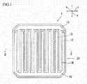
Fig. 1] Fig. 1 is a schematic plan view of a solar cell according to a first embodiment. - [
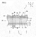
Fig. 2] Fig. 2 is a schematic cross-sectional view of the solar cell taken along the line II-II ofFig. 1 . - [
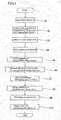
Fig. 3] Fig. 3 is a flowchart showing steps of manufacturing the solar cell according to the first embodiment. - [
Fig. 4] Fig. 4 is a schematic cross-sectional view for describing the steps of manufacturing the solar cell according to the first embodiment. - [
Fig. 5] Fig. 5 is a schematic cross-sectional view for describing the steps of manufacturing the solar cell according to the first embodiment. - [
Fig. 6] Fig. 6 is a schematic cross-sectional view for describing the steps of manufacturing the solar cell according to the first embodiment. - [
Fig. 7] Fig. 7 is a schematic cross-sectional view for describing the steps of manufacturing the solar cell according to the first embodiment. - [
Fig. 8] Fig. 8 is a schematic cross-sectional view for describing the steps of manufacturing the solar cell according to the first embodiment. - [
Fig. 9] Fig. 9 is a schematic cross-sectional view for describing the steps of manufacturing the solar cell according to the first embodiment. - [
Fig. 10] Fig. 10 is a schematic cross-sectional view for describing the steps of manufacturing the solar cell according to the first embodiment. - [
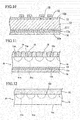
Fig. 11] Fig. 11 is a schematic cross-sectional view of a solar cell according to a second embodiment. - [
Fig. 12] Fig. 12 is a schematic cross-sectional view for describing steps of manufacturing the solar cell according to the second embodiment. - [
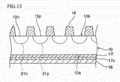
Fig. 13] Fig. 13 is a schematic cross-sectional view for describing the steps of manufacturing the solar cell according to the second embodiment. - Hereinafter, an example of preferred embodiments of the invention is described. Note, however, that the embodiments described below are only an example. The invention is not limited to the embodiments below in any way.
- In addition, in the drawings referenced in the embodiments and the like, members having substantially the same functions are given the same reference numerals. Further, the drawings referenced in the embodiments and the like are schematic. Hence, dimensional ratios and the like of objects depicted in the drawings may be different from actual dimensional ratios and the like of the objects. The dimensional ratios and the like of the objects in the drawings may be different among the drawings as well. Thus, specific dimensional ratios and the like of the objects should be determined in consideration of the following description.
- First of all, the configuration of
solar cell 1 manufactured in this embodiment is described in detail with reference toFigs. 1 and2 . -
Solar cell 1 is a back contact solar cell. Note that, if a sufficient output cannot be obtained from singlesolar cell 1 of this embodiment, a solar cell module made by connecting multiplesolar cells 1 with wiring members may be used. - As shown in
Fig. 2 ,solar cell 1 includessolar cell substrate 20.Solar cell substrate 20 includes:semiconductor substrate 10; and p-typeamorphous semiconductor layer 13 and n-typeamorphous semiconductor layer 12 respectively disposed in certain regions on one surface ofsemiconductor substrate 10. - Note that, an "amorphous semiconductor" in the invention includes a microcrystalline semiconductor. A microcrystalline semiconductor indicates an amorphous semiconductor including a large number of fine crystal grains.
-
Semiconductor substrate 10 includes: light-receivingsurface 10a; andback surface 10b constituting a second principal surface ofsolar cell substrate 20.Semiconductor substrate 10 generates carriers by receivinglight 11 on light-receivingsurface 10a. Here, carriers refer to holes and electrons generated when light is absorbed bysemiconductor substrate 10. -
Semiconductor substrate 10 is formed of a crystalline semiconductor substrate of n-type or p-type conductivity. Specific examples of the crystalline semiconductor substrate include crystalline silicon substrates such as a monocrystalline silicon substrate and a polycrystalline silicon substrate, for example. Hereinbelow, this embodiment describes an example in whichsemiconductor substrate 10 is formed of an n-type crystalline silicon substrate. - On
back surface 10b ofsemiconductor substrate 10, n-typeamorphous semiconductor layer 12 containing an n-type dopant is disposed in a first region whereas p-typeamorphous semiconductor layer 13 containing a p-type dopant is disposed in a second region. Surfaces of these n-typeamorphous semiconductor layer 12 and p-typeamorphous semiconductor layer 13 respectively form n-type surface 12n and p-type surface 13p on a first principal surface ofsolar cell substrate 20. - Note that, n-type
amorphous semiconductor layer 12 and p-typeamorphous semiconductor layer 13 preferably contain hydrogen. Specifically, n-typeamorphous semiconductor layer 12 and p-typeamorphous semiconductor layer 13 are preferably made of hydrogenated amorphous silicon. The thickness of each of n-typeamorphous semiconductor layer 12 and p-typeamorphous semiconductor layer 13 may be about 20 angstroms to 500 angstroms, for example. - In the invention, the "n-type surface" indicates an exposed surface of the semiconductor part of n-type conductivity; the "p-type surface" indicates an exposed surface of the semiconductor part of p-type conductivity.
- Each of n-type
amorphous semiconductor layer 12 and p-typeamorphous semiconductor layer 13 is formed in a comb-teeth shape. Onback surface 10b, n-typeamorphous semiconductor layer 12 and p-typeamorphous semiconductor layer 13 are arranged alternately in direction x perpendicular to intersecting width direction y. N-typeamorphous semiconductor layer 12 and p-typeamorphous semiconductor layer 13 adjacent in direction x are electrically insulated from each other byinsulation layer 18 described later. This makes recombination of minority carriers less likely to occur, whereby high photoelectric conversion efficiency can be achieved. - Note that, in this embodiment, n-type
amorphous semiconductor layer 12 and p-typeamorphous semiconductor layer 13 cover substantiallyentire back surface 10b and constitute the first principal surface ofsolar cell substrate 20. - Each of width W1 of n-type
amorphous semiconductor layer 12 and width W2 of p-typeamorphous semiconductor layer 13 may be about 100 µm to 1.5 mm, for example. Width W1 and interval W2 may be equal and may be different. Here, it is preferable that width W2 of p-typeamorphous semiconductor layer 13 of different conductivity from that ofsemiconductor substrate 10 be larger than width W1 of n-typeamorphous semiconductor layer 12 of the same conductivity as that ofsemiconductor substrate 10. - In addition, an intrinsic amorphous semiconductor (an intrinsic semiconductor is hereinafter referred to as an "i-type semiconductor") layer having a thickness of about several angstroms to 250 angstroms for example, which virtually does not contribute to power generation, may be formed between
semiconductor substrate 10 and each of n-typeamorphous semiconductor layer 12 and p-typeamorphous semiconductor layer 13. The i-type amorphous semiconductor layer may be formed of i-type amorphous silicon containing hydrogen, for example. - In this embodiment, p-type
amorphous semiconductor layer 13 is disposed above each of both end portions in x direction of n-typeamorphous semiconductor layer 12.Insulation layer 18 is disposed in a space formed between portions of n-typeamorphous semiconductor layer 12 and p-typeamorphous semiconductor layer 13 overlapping each other in z direction. Width W3 ofinsulation layer 18 in direction x is not particularly limited, but may be set about one-third of width W1 for example. Interval W4 ofinsulation layer 18 in direction x is also not particularly limited, but may be set about one-third of width W1 for example. - A material of
insulation layer 18 is not particularly limited. For example,insulation layer 18 may be made of silicon oxide, silicon nitride, or silicon oxynitride. Among these,insulation layer 18 is preferably made of silicon nitride. Further,insulation layer 18 preferably contains hydrogen. - N-
side electrode 14 for collecting electrons is disposed on n-typeamorphous semiconductor layer 12, whereas p-side electrode 15 for collecting holes is disposed on p-typeamorphous semiconductor layer 13. These n-side electrode 14 and p-side electrode 15 are insulated from each other above the surface ofinsulation layer 18. - Here, interval W5 formed between n-
side electrode 14 and p-side electrode 15 aboveinsulation layer 18 may be set about one-third of width W3, for example. - As described previously, in this embodiment, each of n-type
amorphous semiconductor layer 12 and p-typeamorphous semiconductor layer 13 is formed in a comb-teeth shape. Hence, each of n-side electrode 14 and p-side electrode 15 is formed in a comb-teeth shape including a bus bar portion and multiple finger portions. Instead, each of n-side electrode 14 and p-side electrode 15 may be a so-called bus-bar-less electrode formed only of multiple finger portions without a bus bar portion. - Note that, a material and a structure of each of n-
side electrode 14 and p-side electrode 15 are not particular limited as long as these are capable of collecting carriers. Each of n-side electrode 14 and p-side electrode 15 may be made of a conductive material such as Transparent Conductive Oxide (TCO) , metal such as Ag, Cu, Sn, Pt, or Au, or an alloy containing one or more of these types of metal, for example. Alternatively, each of n-side electrode 14 and p-side electrode 15 may be formed of a multilayer including multiple conductive films. In this case, n-side electrode 14 or p-side electrode 15 is preferably formed of: a laminated body including a TCO layer formed on n-typeamorphous semiconductor layer 12 or p-typeamorphous semiconductor layer 13; and at least one metal or alloy layer formed on the TCO layer. - The method of forming each of n-
side electrode 14 and p-side electrode 15 is also not particularly limited. Each of n-side electrode 14 and p-side electrode 15 may be formed by, for example, a thin-film formation method such as a sputtering method, a CVD method, or another deposition method, a plating method, or a combination of these methods. - Light-receiving
surface 10a ofsemiconductor substrate 10, which constitutes a second principal surface ofsolar cell substrate 20, has a texture structure. Here, a texture structure refers to a bumpy structure formed to reduce surface reflection and increase the amount of optical absorption bysolar cell substrate 20. For example, the texture structure is a pyramidal (quadrangular pyramidal/truncated quadrangular pyramidal) bumpy structure made by performing anisotropic etching on a monocrystalline silicon substrate having a (100) plane. - 1-type
amorphous semiconductor layer 17i is disposed on textured light-receivingsurface 10a. In this embodiment, i-typeamorphous semiconductor layer 17i is specifically made of i-type amorphous silicon containing hydrogen. The thickness of i-typeamorphous semiconductor layer 17i is not particularly limited as long as this virtually does not contribute to power generation. The thickness of i-typeamorphous semiconductor layer 17i may be about several angstroms to 250 angstroms, for example. - N-type
amorphous semiconductor layer 17n having the same conductivity assemiconductor substrate 10 is disposed on i-typeamorphous semiconductor layer 17i. N-typeamorphous semiconductor layer 17n is an amorphous semiconductor layer of n-type conductivity containing an n-type dopant. More specifically, in this embodiment, n-typeamorphous semiconductor layer 17n is made of n-type amorphous silicon containing hydrogen. The thickness of n-typeamorphous semiconductor layer 17n is not particularly limited, but may be about 20 angstroms to 500 angstroms, for example. -
Insulation layer 16 serving both as an antireflection film and a protection film is formed on n-typeamorphous semiconductor layer 17n.Insulation layer 16 may be made of a material such as silicon oxide, silicon nitride, or silicon oxynitride, for example. The thickness ofinsulation layer 16 may be set as appropriate according to antireflection characteristics intended to be given to this layer. The thickness ofinsulation layer 16 may be selected as appropriate from the range of 80 nm to 1 µm, for example. - Subsequently, a method of manufacturing
solar cell 1 of this embodiment is described with referring mainly toFigs. 3 to 10 . - First of all,
semiconductor substrate 10 having light-receivingsurface 10a and backsurface 10b is prepared. Next, in Step S1, light-receivingsurface 10a and backsurface 10b ofsemiconductor substrate 10 are cleansed.Semiconductor substrate 10 may be cleansed using a HF aqueous solution, for example. Light-receivingsurface 10a and backsurface 10b ofsemiconductor substrate 10 subjected to cleansing each have a substantially flat surface. - Next, in Step S2, n-type
amorphous semiconductor layer 21 andinsulation film 22 are formed in this order on substantiallyentire back surface 10b ofsemiconductor substrate 10. The method of forming each of n-typeamorphous semiconductor layer 21 andinsulation film 22 is not particularly limited. N-typeamorphous semiconductor layer 21 may be formed by a thin-film formation method such as a Chemical Vapor Deposition (CVD) method typified by a plasma CVD method, for example. In the meantime,insulation film 22 may be formed by a thin-film formation method such as a sputtering method or a CVD method, for example. In order to reduce manufacturing costs or prevent impurities from getting mixed in these layer and film, it is preferable to form n-typeamorphous semiconductor layer 21 andinsulation film 22 consecutively while maintaining a vacuum state. - Then, in Step S3, a texture structure is formed in light-receiving
surface 10a ofsemiconductor substrate 10 constituting the second principal surface ofsolar cell substrate 20. The method of forming the texture structure is not particularly limited. For example, the texture structure may be formed by etching light-receivingsurface 10a ofsemiconductor substrate 10 with an etching agent. More specifically, the texture structure may be formed in light-receivingsurface 10a by immersingsemiconductor substrate 10 in an etchant or by placingsemiconductor substrate 10 in an etching gas, for example. - In this Step S3, back
surface 10b ofsemiconductor substrate 10 is coated withinsulation film 22. The etching rate ofinsulation film 22 with an etching agent is lower than the etching rate ofsemiconductor substrate 10. For this reason,insulation film 22 acts as a protection film, and protects n-typeamorphous semiconductor layer 21 and backsurface 10b favorably. Thereby, n-typeamorphous semiconductor layer 21 and backsurface 10b are prevented from being etched with the etching agent. As a result, backsurface 10b ofsemiconductor substrate 10 is kept substantially flat. Thisinsulation film 22 is processed in a later step and becomesinsulation layer 18 being a component ofsolar cell 1. N-typeamorphous semiconductor layer 21 is also processed in a later step and becomes n-typeamorphous semiconductor layer 12. - As described above, this embodiment makes it possible to favorably protect back
surface 10b upon forming the texture structure, by using a member used for forming a component ofsolar cell 1 and without additionally forming a protection layer for protecting backsurface 10b. Accordingly, the manufacturing method of this embodiment enablessolar cell 1 to be manufactured easily and in fewer steps. - Note that, an "etching agent" in the invention includes an etchant, etching paste, etching ink, and so on.
- In addition, although any of a wet etching method and a dry etching method may be used to etch the back surface of the semiconductor substrate in the invention, it is preferable to use wet etching to etch the back surface of the semiconductor substrate from the viewpoint of productivity.
- One of etching agents used favorably for forming the texture structure is an anisotropic etching solution. In the case where a monocrystalline silicon substrate having a (100) plane is used as
semiconductor substrate 10, an alkali solution such as an NaOH solution or a KOH solution may be used as an anisotropic etching solution, for example. - An isotropic etching solution may also be used favorably for forming the texture structure. Any solution may be used for forming the texture structure as long as this is generally used to perform isotropic etching on a semiconductor wafer.
- Specific examples of an isotropic etching solution favorably used include HF, HNO3, or a mixture of these. In addition, phosphoric acid, acetic acid, or a mixture of each of these and water is favorably used as an isotropic etching solution. As an etching agent, a mixed reaction gas of a fluorine-based gas such as CF4 or NF3 and a chlorine-based gas such as CI2 may also be used.
- The etching rate of
semiconductor substrate 10 with an etching agent is preferably 1.1 times or more higher than, more preferably 1.5 times or more higher than, or still more preferably 2 times or more higher than the etching rate ofinsulation film 22 with an etching agent, although it varies depending on the thickness ofinsulation film 22. - Next, in Step S4,
insulation film 22 is subjected to removal processing by used of a predetermined pattern to remove part ofinsulation film 22. More specifically, a portion ofinsulation film 22, which is located in a region where the p-type amorphous semiconductor layer is to be joined tosemiconductor substrate 10 in the following step, is removed. -
Insulation film 22 may be removed by etching, for example. An etching agent used for etching is preferably one such that the etching rate ofinsulation film 22 is higher than the etching rate ofsemiconductor substrate 10. An etching agent used for etchinginsulation film 22 is one such that the etching rate ofinsulation film 22 is preferably 1.1 times or more higher than, more preferably 1.5 times or more higher than, or still more preferably 2 times or more higher than the etching rate ofsemiconductor substrate 10. - To be more specific, in the case where
insulation film 22 is made of silicon oxide, silicon nitride, or silicon oxynitride,insulation film 22 may be etched using an acid etchant such as an HF aqueous solution. - Thereafter, in Step S5, a part of n-type
amorphous semiconductor layer 21 is removed with patternedinsulation film 22 patterned in Step S4 used as a mask, whereby n-typeamorphous semiconductor layer 21 is removed except for a portion covered withinsulation film 22. In this way, backsurface 10b is exposed except for a portion havinginsulation film 22 above, and n-typeamorphous semiconductor layer 12 is formed out ofsemiconductor layer 21. Here, n-typeamorphous semiconductor layer 21 may be removed by etching, for example. Examples of an etching agent preferably used for etching n-typeamorphous semiconductor layer 21 include an alkali etchant containing sodium hydroxide, for example. - Subsequently, in Step S6, i-type
amorphous semiconductor layer 17i, n-typeamorphous semiconductor layer 17n, andinsulation layer 16 are formed in this order on substantially entire light-receivingsurface 10a ofsemiconductor substrate 10 having the texture structure. Semiconductor layers 17i and 17n may be formed by a CVD method such as a plasma CVD method, for example. On the other hand,insulation layer 16 may be formed by a thin-film formation method such as a sputtering method or a CVD method, for example. In order to reduce manufacturing costs or prevent impurities from getting mixed in these layers, it is preferable to form i-typeamorphous semiconductor layer 17i, n-typeamorphous semiconductor layer 17n, andinsulation layer 16 consecutively while maintaining a vacuum state. - Next, in Step S7, p-type
amorphous semiconductor layer 23 is formed to cover backsurface 10b and the surface ofinsulation film 22. The method of forming p-typeamorphous semiconductor layer 23 is not particularly limited. P-typeamorphous semiconductor layer 23 may be formed by a thin-film formation method such as a CVD method, for example. - Then, in Step S8, a portion of p-type
amorphous semiconductor layer 23 located oninsulation film 22 is removed by etching or the like. Thereby, p-typeamorphous semiconductor layer 13 is formed out of p-typeamorphous semiconductor layer 23. - An etching agent used in this Step S8 is one such that the etching rate of
amorphous semiconductor layer 23 is higher than the etching rate ofinsulation film 22. Due to this, ofinsulation film 22 andamorphous semiconductor layer 23,amorphous semiconductor layer 23 is selectively etched. - An etching agent used in Step S8 is one such that the etching rate of p-type
amorphous semiconductor layer 23 is 1.1 times or more higher than, preferably 1.5 times or more higher than, or more preferably 2 times or more higher than the etching rate ofinsulation film 22. Still more preferably, an etching agent used in Step S8 is one with which p-typeamorphous semiconductor layer 23 is etched butinsulation film 22 is not substantially etched. In the case where p-typeamorphous semiconductor layer 23 is made of silicon andinsulation film 22 is made of silicon oxide, silicon nitride, or silicon oxynitride, specific examples of such an etching agent include an alkali aqueous solution such as an NaOH aqueous solution containing NaOH, for example. - Thereafter, in Step S9,
insulation film 22 is removed by etching or the like. More specifically, whileamorphous semiconductor layer 13 formed out ofamorphous semiconductor layer 23 part of which is removed by etching in Step S8 is used as a mask, an exposed portion ofinsulation film 22 is etched with an etching agent and removed. Thereby,insulation layer 18 is formed out ofinsulation film 22, and part of n-typeamorphous semiconductor layer 12 is exposed. Here, one of etching agents preferably used to removeinsulation film 22 is an HF aqueous solution, for example. - Subsequently, in Step S10, an electrode formation step(s) is performed in which n-
side electrode 14 and p-side electrode 15 are formed respectively on n-typeamorphous semiconductor layer 12 and p-typeamorphous semiconductor layer 13. Thus,solar cell 1 is completed. - The method of forming each of n-
side electrode 14 and p-side electrode 15 may be selected as appropriate according to materials of the electrodes. Each of n-side electrode 14 and p-side electrode 15 may be formed by a thin-film formation method such as a sputtering method, a CVD method, or another deposition method, a plating method, a method of coating conductive paste, or a combination of these methods, for example. Alternatively, n-side electrode 14 and p-side electrode 15 may be formed by, for example, forming a conductive layer in such a way that the conductive layer covers n-typeamorphous semiconductor layer 12 and p-typeamorphous semiconductor layer 13, and dividing the conductive layer at positions oninsulation layer 18. In this case, n-side electrode 14 and p-side electrode 15 can be formed at small pitches and with high accuracy in shape. - As described above, in this embodiment,
insulation film 22 for protecting backsurface 10b upon forming the texture structure in light-receivingsurface 10a also acts as an insulation film for electrically isolating n-side electrode 14 and p-side electrode 15 from each other. Accordingly, this embodiment makes it possible to favorably protect backsurface 10b when the texture structure is formed, by using a member used for forming one of the components ofsolar cell 1, without forming an additional protection film for protecting backsurface 10b. Thus, the manufacturing method of this embodiment enablessolar cell 1 to be manufactured easily and in fewer steps. - Hereinafter, another example of preferred embodiments of the invention is described. Note that, in the following description, members having substantially the same functions as those of the first embodiment are given the same reference numerals and description thereof is omitted.
- In the first embodiment, a description is given of an example where
solar cell substrate 20 includessemiconductor substrate 10 and amorphous semiconductor layers 12 and 13. However, the invention is not limited to this configuration. For example, as shown inFig. 11 ,solar cell substrate 20 may includesemiconductor substrate 10 in which p-typedopant diffusion portion 31n and n-typedopant diffusion portion 31p exposed toback surface 10b are formed. In this case,solar cell 1 may be manufactured in the following way. - First, p-type diffusion paste is used to diffuse a p-type dopant in
semiconductor substrate 10 from one portion of one principal surface thereof, and n-type diffusion paste is used to diffuse an n-type dopant insemiconductor substrate 10 from at least part of the other portion of the one principal surface. With this process, p-typedopant diffusion portion 31n and n-typedopant diffusion portion 31p are formed insemiconductor substrate 10, andsolar cell substrate 20 is thus obtained. - Next, as shown in
Fig. 12 ,insulation film 22 is formed onback surface 10b ofsemiconductor substrate 10. Thereafter, a texture structure is formed in light-receivingsurface 10a ofsemiconductor substrate 10. - Then, as shown in
Fig. 13 , p-typedopant diffusion portion 31n and n-typedopant diffusion portion 31p are exposed by removing at least part of a portion ofinsulation film 22, the portion being located on p-typedopant diffusion portion 31n and n-typedopant diffusion portion 31p. - After that, n-
side electrode 14 and p-side electrode 15 are formed on p-typedopant diffusion portion 31n and n-typedopant diffusion portion 31p, thereby completing the solar cell. - In this embodiment as well,
insulation film 22 for protecting backsurface 10b when the texture structure is formed also acts as an insulation film for electrically isolating n-side electrode 14 and p-side electrode 15 from each other and as a passivation film forsemiconductor substrate 10. - Accordingly, this embodiment also makes it possible to protect back
surface 10b favorably when a texture structure is formed, by using a member used for forming a component ofsolar cell 1 and without additionally forming a protection layer for protecting backsurface 10b. Thus, the manufacturing method of this embodiment enablessolar cell 1 to be manufactured easily and in fewer steps. -
- 1
- solar cell
- 10
- semiconductor substrate
- 10a
- light-receiving surface
- 10b
- back surface
- 12
- n-type amorphous semiconductor layer
- 12n
- n-type surface
- 13
- p-type amorphous semiconductor layer
- 13p
- p-type surface
- 14
- n-side electrode
- 15
- p-side electrode
- 18
- insulation layer
- 20
- solar cell substrate
- 21
- n-type amorphous semiconductor layer
- 22
- insulation film
- 23
- p-type amorphous semiconductor layer
- 31n
- p-type dopant diffusion portion
- 31p
- n-type dopant diffusion portion
Claims (11)
- A method to manufacture a solar cell including: a solar cell substrate including a semiconductor substrate, a first principal surface with a p-type surface and an n-type surface, and a textured second principal surface; a p-side electrode disposed on the p-type surface; an n-side electrode disposed on the n-type surface; and an insulation layer formed on the first principal surface and isolating the p-side electrode and the n-side electrode from each other, the method comprising:forming an insulation film covering the first principal surface, and then forming the texture structure in the second principal surface; andremoving part of the insulation film, and thereby forming the insulation layer.
- The method of manufacturing the solar cell according to claim 1, wherein the insulation film is used as a protection film protecting the first principal surface when the texture structure is formed in the second principal surface.
- The manufacturing method according to claim 1 or 2, wherein
the texture structure is formed by etching the second principal surface with an etching agent, and
the insulation film formed is an insulation film whose etching rate with the etching agent is lower than an etching rate of the semiconductor substrate with the etching agent. - The manufacturing method according to any one of claims 1 to 3, wherein the insulation film is made of any one of silicon oxide, silicon nitride, and silicon oxynitride.
- The manufacturing method according to any one of claims 1 to 4, further comprising:forming a first semiconductor layer of a first conductivity on one principal surface of the semiconductor substrate;forming the insulation film on the first semiconductor layer;forming the texture structure in the other principal surface of the semiconductor substrate;partly removing the insulation film and the first semiconductor layer to thereby expose part of the first principal surface; andforming a second semiconductor layer of a second conductivity on the exposed part of the first principal surface, thereby obtaining the solar cell substrate including the semiconductor substrate, the first semiconductor layer, and the second semiconductor layer.
- The manufacturing method according to claim 5, wherein
the second semiconductor layer is formed to cover the exposed part and the insulation layer,
the first semiconductor layer is exposed by partly removing the insulation film and a portion of the second semiconductor layer located on the insulation film, and then
the p-side electrode and the n-side electrode are formed. - The manufacturing method according to claim 5 or 6, wherein the p-side electrode and the n-side electrode are formed by:forming a conductive layer covering the first and second semiconductor layers and the insulation layer, anddividing the conductive layer at positions on the insulation layer.
- The manufacturing method according to any one of claims 5 to 7, wherein at least one of the first and second semiconductor layers is made of an amorphous semiconductor.
- The manufacturing method according to claim 8, further comprising
forming an intrinsic amorphous semiconductor layer between the semiconductor substrate and at least one of the first and second semiconductor layers made of the amorphous semiconductor. - The manufacturing method according to any one of claims 1 to 4, further comprising:diffusing a p-type dopant in the semiconductor substrate from one portion of one principal surface thereof, and diffusing an n-type dopant in the semiconductor substrate from at least part of the other portion of the one principal surface; andforming the texture structure in the other principal surface, thereby obtaining the solar cell substrate.
- The manufacturing method according to any one of claims 1 to 10, wherein a crystalline semiconductor substrate is used as the semiconductor substrate.
Applications Claiming Priority (2)
| Application Number | Priority Date | Filing Date | Title |
|---|---|---|---|
| JP2010215917A JP5595850B2 (en) | 2010-09-27 | 2010-09-27 | Manufacturing method of solar cell |
| PCT/JP2011/068374 WO2012043080A1 (en) | 2010-09-27 | 2011-08-11 | Process for manufacturing solar cell |
Publications (2)
| Publication Number | Publication Date |
|---|---|
| EP2624306A1 true EP2624306A1 (en) | 2013-08-07 |
| EP2624306A4 EP2624306A4 (en) | 2017-06-14 |
Family
ID=45892555
Family Applications (1)
| Application Number | Title | Priority Date | Filing Date |
|---|---|---|---|
| EP11828641.8A Withdrawn EP2624306A4 (en) | 2010-09-27 | 2011-08-11 | Process for manufacturing solar cell |
Country Status (4)
| Country | Link |
|---|---|
| US (1) | US8865510B2 (en) |
| EP (1) | EP2624306A4 (en) |
| JP (1) | JP5595850B2 (en) |
| WO (1) | WO2012043080A1 (en) |
Families Citing this family (9)
| Publication number | Priority date | Publication date | Assignee | Title |
|---|---|---|---|---|
| JP5974300B2 (en) * | 2010-08-24 | 2016-08-23 | パナソニックIpマネジメント株式会社 | Solar cell and manufacturing method thereof |
| JPWO2012132835A1 (en) * | 2011-03-25 | 2014-07-28 | 三洋電機株式会社 | Solar cell |
| JP5999527B2 (en) * | 2012-04-26 | 2016-09-28 | パナソニックIpマネジメント株式会社 | Solar cell module and method for manufacturing solar cell module |
| DE112012006445B4 (en) | 2012-05-31 | 2021-10-21 | Panasonic Intellectual Property Management Co., Ltd. | Manufacturing process for solar cell |
| JP6476015B2 (en) * | 2015-03-06 | 2019-02-27 | シャープ株式会社 | Photoelectric conversion element and manufacturing method thereof |
| WO2018056143A1 (en) * | 2016-09-23 | 2018-03-29 | 昭和電工株式会社 | Solar battery cell manufacturing method |
| US10141462B2 (en) | 2016-12-19 | 2018-11-27 | Sunpower Corporation | Solar cells having differentiated P-type and N-type architectures |
| CN118507572B (en) * | 2024-05-08 | 2024-12-31 | 隆基绿能科技股份有限公司 | Battery piece, battery string and photovoltaic module |
| AU2025263802B2 (en) * | 2024-06-14 | 2026-06-11 | Longi Green Energy Technology Co., Ltd. | Back contact cell and method for manufacturing same |
Family Cites Families (9)
| Publication number | Priority date | Publication date | Assignee | Title |
|---|---|---|---|---|
| JP2006324590A (en) * | 2005-05-20 | 2006-11-30 | Sharp Corp | Back electrode type solar cell and manufacturing method thereof |
| JP4767110B2 (en) * | 2006-06-30 | 2011-09-07 | シャープ株式会社 | Solar cell and method for manufacturing solar cell |
| JP5226255B2 (en) * | 2007-07-13 | 2013-07-03 | シャープ株式会社 | Manufacturing method of solar cell |
| JP5277485B2 (en) * | 2007-12-13 | 2013-08-28 | シャープ株式会社 | Manufacturing method of solar cell |
| EP2239788A4 (en) * | 2008-01-30 | 2017-07-12 | Kyocera Corporation | Solar battery element and solar battery element manufacturing method |
| JP5347409B2 (en) | 2008-09-29 | 2013-11-20 | 三洋電機株式会社 | Solar cell and manufacturing method thereof |
| US8288645B2 (en) * | 2009-03-17 | 2012-10-16 | Sharp Laboratories Of America, Inc. | Single heterojunction back contact solar cell |
| WO2010113750A1 (en) * | 2009-03-30 | 2010-10-07 | 三洋電機株式会社 | Solar cell |
| KR20130094728A (en) * | 2010-05-24 | 2013-08-26 | 더 트러스티즈 오브 프린스턴 유니버시티 | Photovoltaic device and method of making same |
-
2010
- 2010-09-27 JP JP2010215917A patent/JP5595850B2/en active Active
-
2011
- 2011-08-11 WO PCT/JP2011/068374 patent/WO2012043080A1/en not_active Ceased
- 2011-08-11 EP EP11828641.8A patent/EP2624306A4/en not_active Withdrawn
-
2013
- 2013-03-21 US US13/848,192 patent/US8865510B2/en active Active
Non-Patent Citations (1)
| Title |
|---|
| See references of WO2012043080A1 * |
Also Published As
| Publication number | Publication date |
|---|---|
| EP2624306A4 (en) | 2017-06-14 |
| US20130210187A1 (en) | 2013-08-15 |
| WO2012043080A1 (en) | 2012-04-05 |
| JP5595850B2 (en) | 2014-09-24 |
| JP2012074415A (en) | 2012-04-12 |
| US8865510B2 (en) | 2014-10-21 |
Similar Documents
| Publication | Publication Date | Title |
|---|---|---|
| US8865510B2 (en) | Method of manufacturing solar cell | |
| EP2434548B1 (en) | Solar cell and method for manufacturing the same | |
| US9142706B2 (en) | Method of manufacturing solar cell | |
| CN103283033B (en) | The manufacture method of solar cell and solar cell | |
| EP3349253B1 (en) | Semiconductor devices and methods for manufacturing the same | |
| EP2065941A2 (en) | Solar cell and a manufacturing method of the solar cell | |
| US8877545B2 (en) | Method of manufacturing solar cell | |
| EP2600414A1 (en) | Process for production of solar cell, and solar cell | |
| JP5388970B2 (en) | Manufacturing method of solar cell | |
| US20140020742A1 (en) | Photoelectric conversion device and method for producing photoelectric conversion device | |
| US9997647B2 (en) | Solar cells and manufacturing method thereof | |
| US9653626B2 (en) | Photoelectric conversion device and method for producing photoelectric conversion device | |
| US9419168B2 (en) | Method of manufacturing a solar cell by texturing a principal surface using an alkaline solution | |
| EP2690667A1 (en) | Method for producing photoelectric conversion device | |
| JP5275415B2 (en) | Crystal solar cell and method for manufacturing crystal solar cell | |
| JP2005260157A (en) | Solar cell and solar cell module | |
| EP2690669A1 (en) | Solar cell | |
| WO2012132834A1 (en) | Solar cell and method for producing solar cell | |
| JP2009081470A (en) | Solar cell and solar cell module | |
| WO2012117825A1 (en) | Solar cell and process of manufacturing solar cell | |
| JP5129369B2 (en) | Crystal solar cell and method for manufacturing crystal solar cell |
Legal Events
| Date | Code | Title | Description |
|---|---|---|---|
| PUAI | Public reference made under article 153(3) epc to a published international application that has entered the european phase |
Free format text: ORIGINAL CODE: 0009012 |
|
| 17P | Request for examination filed |
Effective date: 20130417 |
|
| AK | Designated contracting states |
Kind code of ref document: A1 Designated state(s): AL AT BE BG CH CY CZ DE DK EE ES FI FR GB GR HR HU IE IS IT LI LT LU LV MC MK MT NL NO PL PT RO RS SE SI SK SM TR |
|
| DAX | Request for extension of the european patent (deleted) | ||
| RAP1 | Party data changed (applicant data changed or rights of an application transferred) |
Owner name: PANASONIC INTELLECTUAL PROPERTY MANAGEMENT CO., LT |
|
| RA4 | Supplementary search report drawn up and despatched (corrected) |
Effective date: 20170517 |
|
| RIC1 | Information provided on ipc code assigned before grant |
Ipc: H01L 31/068 20120101ALI20170511BHEP Ipc: H01L 31/20 20060101ALI20170511BHEP Ipc: H01L 31/0224 20060101ALI20170511BHEP Ipc: H01L 31/04 20140101AFI20170511BHEP Ipc: H01L 31/0747 20120101ALI20170511BHEP Ipc: H01L 31/18 20060101ALI20170511BHEP |
|
| STAA | Information on the status of an ep patent application or granted ep patent |
Free format text: STATUS: REQUEST FOR EXAMINATION WAS MADE |
|
| STAA | Information on the status of an ep patent application or granted ep patent |
Free format text: STATUS: THE APPLICATION IS DEEMED TO BE WITHDRAWN |
|
| 18D | Application deemed to be withdrawn |
Effective date: 20171213 |