EP2624288A2 - Semiconductor package with improved testability - Google Patents
Semiconductor package with improved testability Download PDFInfo
- Publication number
- EP2624288A2 EP2624288A2 EP12006188.2A EP12006188A EP2624288A2 EP 2624288 A2 EP2624288 A2 EP 2624288A2 EP 12006188 A EP12006188 A EP 12006188A EP 2624288 A2 EP2624288 A2 EP 2624288A2
- Authority
- EP
- European Patent Office
- Prior art keywords
- package
- semiconductor package
- contacts
- testing
- conductive medium
- Prior art date
- Legal status (The legal status is an assumption and is not a legal conclusion. Google has not performed a legal analysis and makes no representation as to the accuracy of the status listed.)
- Granted
Links
Images




Classifications
-
- H—ELECTRICITY
- H10—SEMICONDUCTOR DEVICES; ELECTRIC SOLID-STATE DEVICES NOT OTHERWISE PROVIDED FOR
- H10W—GENERIC PACKAGES, INTERCONNECTIONS, CONNECTORS OR OTHER CONSTRUCTIONAL DETAILS OF DEVICES COVERED BY CLASS H10
- H10W72/00—Interconnections or connectors in packages
-
- H—ELECTRICITY
- H10—SEMICONDUCTOR DEVICES; ELECTRIC SOLID-STATE DEVICES NOT OTHERWISE PROVIDED FOR
- H10P—GENERIC PROCESSES OR APPARATUS FOR THE MANUFACTURE OR TREATMENT OF DEVICES COVERED BY CLASS H10
- H10P74/00—Testing or measuring during manufacture or treatment of wafers, substrates or devices
- H10P74/27—Structural arrangements therefor
- H10P74/273—Interconnections for measuring or testing, e.g. probe pads
-
- H—ELECTRICITY
- H10—SEMICONDUCTOR DEVICES; ELECTRIC SOLID-STATE DEVICES NOT OTHERWISE PROVIDED FOR
- H10P—GENERIC PROCESSES OR APPARATUS FOR THE MANUFACTURE OR TREATMENT OF DEVICES COVERED BY CLASS H10
- H10P74/00—Testing or measuring during manufacture or treatment of wafers, substrates or devices
-
- H—ELECTRICITY
- H10—SEMICONDUCTOR DEVICES; ELECTRIC SOLID-STATE DEVICES NOT OTHERWISE PROVIDED FOR
- H10W—GENERIC PACKAGES, INTERCONNECTIONS, CONNECTORS OR OTHER CONSTRUCTIONAL DETAILS OF DEVICES COVERED BY CLASS H10
- H10W70/00—Package substrates; Interposers; Redistribution layers [RDL]
- H10W70/60—Insulating or insulated package substrates; Interposers; Redistribution layers
- H10W70/62—Insulating or insulated package substrates; Interposers; Redistribution layers characterised by their interconnections
- H10W70/63—Vias, e.g. via plugs
- H10W70/635—Through-vias
-
- H—ELECTRICITY
- H10—SEMICONDUCTOR DEVICES; ELECTRIC SOLID-STATE DEVICES NOT OTHERWISE PROVIDED FOR
- H10W—GENERIC PACKAGES, INTERCONNECTIONS, CONNECTORS OR OTHER CONSTRUCTIONAL DETAILS OF DEVICES COVERED BY CLASS H10
- H10W74/00—Encapsulations, e.g. protective coatings
- H10W74/01—Manufacture or treatment
- H10W74/014—Manufacture or treatment using batch processing
-
- H—ELECTRICITY
- H10—SEMICONDUCTOR DEVICES; ELECTRIC SOLID-STATE DEVICES NOT OTHERWISE PROVIDED FOR
- H10W—GENERIC PACKAGES, INTERCONNECTIONS, CONNECTORS OR OTHER CONSTRUCTIONAL DETAILS OF DEVICES COVERED BY CLASS H10
- H10W74/00—Encapsulations, e.g. protective coatings
- H10W74/10—Encapsulations, e.g. protective coatings characterised by their shape or disposition
- H10W74/111—Encapsulations, e.g. protective coatings characterised by their shape or disposition the semiconductor body being completely enclosed
- H10W74/114—Encapsulations, e.g. protective coatings characterised by their shape or disposition the semiconductor body being completely enclosed by a substrate and the encapsulations
- H10W74/117—Encapsulations, e.g. protective coatings characterised by their shape or disposition the semiconductor body being completely enclosed by a substrate and the encapsulations the substrate having spherical bumps for external connection
-
- H—ELECTRICITY
- H10—SEMICONDUCTOR DEVICES; ELECTRIC SOLID-STATE DEVICES NOT OTHERWISE PROVIDED FOR
- H10W—GENERIC PACKAGES, INTERCONNECTIONS, CONNECTORS OR OTHER CONSTRUCTIONAL DETAILS OF DEVICES COVERED BY CLASS H10
- H10W90/00—Package configurations
- H10W90/401—Package configurations characterised by multiple insulating or insulated package substrates, interposers or RDLs
-
- H—ELECTRICITY
- H10—SEMICONDUCTOR DEVICES; ELECTRIC SOLID-STATE DEVICES NOT OTHERWISE PROVIDED FOR
- H10W—GENERIC PACKAGES, INTERCONNECTIONS, CONNECTORS OR OTHER CONSTRUCTIONAL DETAILS OF DEVICES COVERED BY CLASS H10
- H10W90/00—Package configurations
- H10W90/701—Package configurations characterised by the relative positions of pads or connectors relative to package parts
-
- H—ELECTRICITY
- H10—SEMICONDUCTOR DEVICES; ELECTRIC SOLID-STATE DEVICES NOT OTHERWISE PROVIDED FOR
- H10W—GENERIC PACKAGES, INTERCONNECTIONS, CONNECTORS OR OTHER CONSTRUCTIONAL DETAILS OF DEVICES COVERED BY CLASS H10
- H10W70/00—Package substrates; Interposers; Redistribution layers [RDL]
- H10W70/60—Insulating or insulated package substrates; Interposers; Redistribution layers
-
- H—ELECTRICITY
- H10—SEMICONDUCTOR DEVICES; ELECTRIC SOLID-STATE DEVICES NOT OTHERWISE PROVIDED FOR
- H10W—GENERIC PACKAGES, INTERCONNECTIONS, CONNECTORS OR OTHER CONSTRUCTIONAL DETAILS OF DEVICES COVERED BY CLASS H10
- H10W70/00—Package substrates; Interposers; Redistribution layers [RDL]
- H10W70/60—Insulating or insulated package substrates; Interposers; Redistribution layers
- H10W70/62—Insulating or insulated package substrates; Interposers; Redistribution layers characterised by their interconnections
- H10W70/63—Vias, e.g. via plugs
-
- H—ELECTRICITY
- H10—SEMICONDUCTOR DEVICES; ELECTRIC SOLID-STATE DEVICES NOT OTHERWISE PROVIDED FOR
- H10W—GENERIC PACKAGES, INTERCONNECTIONS, CONNECTORS OR OTHER CONSTRUCTIONAL DETAILS OF DEVICES COVERED BY CLASS H10
- H10W72/00—Interconnections or connectors in packages
- H10W72/01—Manufacture or treatment
- H10W72/0198—Manufacture or treatment batch processes
-
- H—ELECTRICITY
- H10—SEMICONDUCTOR DEVICES; ELECTRIC SOLID-STATE DEVICES NOT OTHERWISE PROVIDED FOR
- H10W—GENERIC PACKAGES, INTERCONNECTIONS, CONNECTORS OR OTHER CONSTRUCTIONAL DETAILS OF DEVICES COVERED BY CLASS H10
- H10W72/00—Interconnections or connectors in packages
- H10W72/20—Bump connectors, e.g. solder bumps or copper pillars; Dummy bumps; Thermal bumps
- H10W72/251—Materials
- H10W72/252—Materials comprising solid metals or solid metalloids, e.g. PbSn, Ag or Cu
-
- H—ELECTRICITY
- H10—SEMICONDUCTOR DEVICES; ELECTRIC SOLID-STATE DEVICES NOT OTHERWISE PROVIDED FOR
- H10W—GENERIC PACKAGES, INTERCONNECTIONS, CONNECTORS OR OTHER CONSTRUCTIONAL DETAILS OF DEVICES COVERED BY CLASS H10
- H10W90/00—Package configurations
- H10W90/701—Package configurations characterised by the relative positions of pads or connectors relative to package parts
- H10W90/721—Package configurations characterised by the relative positions of pads or connectors relative to package parts of bump connectors
- H10W90/722—Package configurations characterised by the relative positions of pads or connectors relative to package parts of bump connectors between stacked chips
-
- H—ELECTRICITY
- H10—SEMICONDUCTOR DEVICES; ELECTRIC SOLID-STATE DEVICES NOT OTHERWISE PROVIDED FOR
- H10W—GENERIC PACKAGES, INTERCONNECTIONS, CONNECTORS OR OTHER CONSTRUCTIONAL DETAILS OF DEVICES COVERED BY CLASS H10
- H10W90/00—Package configurations
- H10W90/701—Package configurations characterised by the relative positions of pads or connectors relative to package parts
- H10W90/721—Package configurations characterised by the relative positions of pads or connectors relative to package parts of bump connectors
- H10W90/724—Package configurations characterised by the relative positions of pads or connectors relative to package parts of bump connectors between a chip and a stacked insulating package substrate, interposer or RDL
Definitions
- Testing occurs during or after manufacturing to ensure that semiconductor packages and dies are capable of meeting certain stringent operating requirements and standards.
- Exemplary tests that may be performed on a semiconductor package include various tests for active dies within the package, such as electrical signal timing tests, voltage and current level tests, at-speed tests, direct current tests, bum-in tests, room/cold tests, and hot sort tests.
- the semiconductor package would include at least one active die with interface contacts that are provided to a bottom surface of the semiconductor package.
- the interface contacts may be utilized for regular operation of the semiconductor package (i.e. operation out in the field).
- the active die can include dedicated testing contacts that are also provided to the bottom surface of the semiconductor package. These dedicated testing contacts are utilized for testing, but not for regular operation of the semiconductor package.
- An exemplary testing equipment or device may include a bottom portion and a top portion, where the bottom portion may receive all of the interface contacts and the dedicated testing contacts of the semiconductor package and the top portion may be utilized to physically hold the semiconductor package onto the bottom portion of the testing equipment or device.
- the semiconductor package may then be tested and screened for stringent operating requirements and standards. Subsequently, the semiconductor package may be used in the field in regular operation.
- the present disclosure is directed to a semiconductor package with improved testability, substantially as shown in and/or described in connection with at least one of the figures, and as set forth more completely in the claims.
- a testable semiconductor package comprises:
- said at least one conductive medium is coupled to a package-top testing connection.
- said package-top testing connection comprises a solder ball.
- said at least one conductive medium comprises a conductive via.
- said at least one conductive medium comprises a conductive block.
- At least a portion of said at least one conductive medium is formed in an upper interposer.
- the testable semiconductor package further comprises at least one top metal layer segment providing electrical connection between at least one of said dedicated testing contacts and said at least one conductive medium.
- said interface contacts are electrically connected to package-bottom connections.
- said package-bottom connections comprise solder balls.
- testable semiconductor package further comprises a molding that encloses said active die.
- a testable semiconductor package comprises:
- said at least one conductive medium comprises a conductive block.
- the testable semiconductor package further comprises at least one top metal layer segment providing electrical connection between at least one of said dedicated testing contacts and said at least one conductive medium.
- testable semiconductor package further comprises a molding that encloses said active die.
- a system for testing a semiconductor package, said system comprising:
- said at least one conductive medium is coupled to a package-top testing connection.
- said top testing socket is connected to said at least one of said dedicated testing contacts through a solder ball.
- the system comprises a bottom testing socket connected to at least one package-bottom connection.
- At least one of said interface contacts is electrically connected to said package-bottom connection through said interposer.
- the system comprises a pogo pin connected to said at least one of said dedicated testing contacts.
- Figure 1 presents testable semiconductor package 100 (also referred to as "package 100"), according to an implementation of the present disclosure.
- Package 100 includes active die 102, interposer 104 (or more generally “substrate 104"), conductive mediums 106a and 106b, package-top testing connections 108a and 108b (also referred to collectively as “package-top testing connections 108"), package-bottom connections 110a, 110b, 110c, 110d, and 110e (also referred to collectively as “package-bottom connections 110"), and molding 132.
- Active die 102 has interface contacts 112a, 112b, and 112c (also referred to collectively as “interface contacts 112") and dedicated testing contacts 114a and 114b (also referred to collectively as “dedicated testing contacts 114").
- Active die 102 can include, for example, an integrated circuit (IC), and other electrical components that are connected to interface contacts 112 and dedicated testing contacts 114.
- IC integrated circuit
- at least some of interface contacts 112 and dedicated testing contacts 114 include solder balls (e.g. micro-bumps), as one example.
- Interface contacts 112 are utilized for regular operation of package 100. In other words, interface contacts 112 are for regular operation out in the field. At least some of interface contacts 112 can have additional uses, such as for testing package 100. However, dedicated testing contacts 114 are utilized for testing, but not for regular operation of package 100.
- interface contacts 112 and dedicated testing contacts 114 are shown as being coupled to bottom surface 116a of active die 102, any of interface contacts 112 and dedicated testing contacts 114 can be coupled to different surfaces of active die 102 including top surface 116b. In such implementations, interface contacts 112 and dedicated testing contacts 114 can include bond wires or other connection means. Also, while only active die 102 is shown in Figure 1 , package 100 includes additional active dies in some implementations. The additional dies can have additional interface contacts 112 and dedicated testing contacts 114.
- interposer 104 is situated adjacent bottom surface 116a of active die 102. Interposer 104 is providing electrical connections between interface contacts 112 and bottom surface 118a of package 100.
- interposer 104 includes substrate core 120, top metal layer segments 122a, 122b, 122c, 122d, and 122e (also referred to collectively as “top metal layer segments 122"), top solder mask 124, bottom metal layer segments 126a, 126b, 126c, 126d, and 126e (also referred to collectively as "bottom metal layer segments 126"), bottom solder mask 128, and vias 130a and 130b (also referred to collectively as "vias 130").
- vias 130 are through semiconductor vias (TSVs).
- Substrate 104 include, as examples, an organic-substrate, a laminate substrate, and a ceramic substrate. In the present implementation substrate 104 includes a laminate substrate. Substrate 104 is shown as having top metal layer segments 122 and bottom metal layer segments 126, but can include more than two layers of metal segments.
- interface contacts 112 are electrically connected to package-bottom connections 110 through interposer 104.
- Package-bottom connections 110 are electrically connected to at least some of bottom metal layer segments 126.
- at least some of package-bottom connections 110 are solder balls and can form a ball grid array (BGA).
- package 100 can include different types of package-bottom connections 110 or not include package-bottom connections 110 in various implementations.
- package-bottom connections 110 are situated on at least some of bottom metal layer segments 126 through respective openings in bottom solder mask 128.
- interposer 104 can have many different forms and is presented as one example.
- Package 100 further includes conductive mediums 106 providing electrical connection between dedicated testing contacts 114 and top surface 118b of package 100.
- conductive medium 106a is providing electrical connection between dedicated testing contact 114a and top surface 118b
- conductive medium 106b is providing electrical connection between dedicated testing contact 114b and top surface 118b.
- dedicated testing contacts 114 are available for testing on top surface 118b of package 100.
- bottom surface 118a is considered highly valuable package area. For example, it may be desirable to provide all or most of interface contacts 112 to bottom surface 118a for regular operation of package 100. As one example, it may be easier to deploy package 100 out in the field. However, having dedicated testing contacts 114 provided to bottom surface 118a may, for example, hinder providing some of interface contacts 112 to bottom surface 118a. By providing dedicated testing contacts 114 to top surface 118b of package 100 instead of to bottom surface 118a of package 100, additional space can be created on bottom surface 118a for, for example, interface contacts 112 or for other purposes. As such, in some implementations, it may be easier to provide all or most of interface contacts 112 to bottom surface 118a for regular operation of package 100. Furthermore, it may be possible to provide additional interface contacts 112 to bottom surface 118a, thereby enhancing functionality of package 100. Additionally, it may be possible to reduce the overall footprint or package size of package 100.
- top metal layer segments 122 are providing electrical connection between dedicated testing contacts 114 and conductive mediums 106.
- top metal layer segment 122a is providing electrical connection between dedicated testing contact 114a and conductive medium 106a.
- Conductive mediums 106 are coupled to respective package-top testing connections 108.
- Package-top testing connections 108 are shown as being solder balls. However, some implementations do not include package-top testing connections 108 or include different types of package-top testing connections 108.
- conductive mediums 106 include through mold vias (TMVs) 105a and 105b (also referred to as “conductive via 105a” and “conductive via 105b”) that are situated within molding 132, which encloses active die 102.
- TMVs through mold vias
- conductive mediums 106 traverse bottom surface 116a and top surface 116b of active die 102.
- Forming conductive mediums 106 can include, for example, forming vias through molding 132 and top solder mask 124 and filling the vias with conductive material that can include, as examples, a metal or metal alloy to form TMVs 105a and 105b.
- dedicated testing contacts 114 can be provided to anywhere on top surface 118b, including directly over active die 102. In some implementations, at least some of dedicated testing contacts 114 are on top surface 116b of active die 102 and are provided to top surface 118b using, any suitable conductive medium, such as a TMV.
- package 100 can be, as examples, a fine ball grid array (FBGA) package, a flip chip (FC) package, a quad-flat no-leads (QFN) package, a top probe interposer package, a wafer level package, a package-on-package (PoP) type package, or other type of package not specifically described herein. While implementations shown herein include molding 132, other implementations do not include molding 132. Furthermore, conductive mediums 106 can take many different forms from what is shown in Figure 1 . As another example, Figure 2 presents testable semiconductor package 200 (also referred to as "package 200”), according to an implementation of the present disclosure.
- FBGA fine ball grid array
- FC flip chip
- QFN quad-flat no-leads
- PoP package-on-package
- conductive mediums 106 can take many different forms from what is shown in Figure 1 .
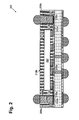
- Figure 2 presents testable semiconductor package 200 (also referred to as "package 200”), according to an implementation of the present disclosure
- Package 200 corresponds to package 100 in Figure 1 . Thus, at least some similar and/or same elements between Figures 1 and 2 are not specifically described with respect to Figure 2 .
- Package 200 includes active die 202, conductive mediums 206a and 206b, dedicated testing contacts 214a and 214b, bottom surface 216a, top surface 216b, top surface 218b, top metal layer segments 222a and 222e, and molding 232 corresponding respectively to active die 102, conductive mediums 106a and 106b, dedicated testing contacts 114a and 114b, bottom surface 116a, top surface 116b, top surface 118b, top metal layer segments 122a and 122e, and molding 132 in Figure 1 .
- conductive medium 206a includes conductive block 234a, which is attached to top metal layer segment 222a using solder 236a.
- conductive medium 206b includes conductive block 234b, which is attached to top metal layer segment 222e using solder 236b.
- Conductive blocks 234a and 234b can include conductive material, such as a metal or metal alloy, and can have any suitable shape.
- conductive blocks 234a and 234b are copper blocks.
- Forming package 200 can include, for example, soldering conductive blocks 234a and 234b to respective top metal layer segments 222a and 222e and subsequently forming molding 232 over conductive blocks 234a and 234b.
- at least some dedicated testing contacts are on top surface 216b of active die 202 and are provided to top surface 218b using, for example, a copper block.
- Figure 3 presents testable semiconductor package 300 (also referred to as "package 300"), according to an implementation of the present disclosure.
- Package 300 corresponds to package 100 in Figure 1 .
- Figures 1 and 3 are not specifically described with respect to Figure 3 .
- Package 300 includes active die 302, lower interposer 304 (or more generally "lower substrate 304"), conductive mediums 306a and 306b, package-top testing connections 308a and 308b, dedicated testing contacts 314a and 314b, bottom surface 316a, top surface 316b, top surface 318b, top metal layer segments 322a and 322e, and molding 332 corresponding respectively to active die 102, interposer 104, conductive mediums 106a and 106b, package-top testing connections 308a and 308b, dedicated testing contacts 114a and 114b, bottom surface 116a, top surface 116b, top surface 118b, top metal layer segments 122a and 122e, and molding 132 in Figure 1 .
- Package 300 also includes upper interposer 340 (or more generally "upper substrate 340") situated adjacent top surface 316b of active die 302.
- Upper interposer 340 can be, as examples, a silicon interposer, a laminate substrate, and the like. As upper interposer 340 is a silicon interposer in the present implementation, upper interposer 340 includes substrate core 342, top metal layer segments 346a and 346b, top solder mask (or passivation) 348, bottom metal layer segments 350a and 350b, bottom solder mask (or passivation) 352, and vias 354a, 354b, and 354c. Vias 354a, 354b, and 354c are through semiconductor vias (TSVs) in the present implementation. Upper interposer 340 can be a similar type of interposer or substrate as lower interposer 304 as shown in Figure 3 , or can be a different type of interposer or substrate as lower interposer 304.
- TSVs semiconductor vias
- conductive medium 306a is formed in upper interposer 340. Additionally, at least a portion of conductive medium 306b is formed in upper interposer 340.
- conductive medium 306a includes top metal layer segment 346a, bottom metal layer segment 350a, via 354a, and interconnect solder ball 344a.
- Conductive medium 306b includes top metal layer segment 346b, bottom metal layer segment 350b, vias 354b and 354c, and interconnect solder ball 344b.
- Top metal layer segments 346a and 346b, bottom metal layer segments 350a and 350b, and vias 354a, 354b, and 354c are formed in upper interposer 340.
- interconnect solder ball 344a is electrically connecting bottom metal layer segment 350a of upper interposer 340 to top metal layer segment 322a of lower interposer 304.
- Package-top testing connection 308a is situated on and electrically connected to top metal layer segment 346a through an opening in top solder mask 348.
- interconnect solder ball 344b is electrically connecting bottom metal layer segment 350b of upper interposer 340 to top metal layer segment 322e of lower interposer 304.
- Package-top testing connection 308b is situated on and electrically connected to top metal layer segment 346b through an opening in top solder mask 348.
- Implementations described with respect to Figures 1 , 2 , and 3 show where at least one conductive medium is providing electrical connection between at least one dedicated testing contact and a top surface of a testable semiconductor package. Additionally, or instead, in some implementations, at least one conductive medium is providing electrical connection between at least one dedicated testing contact and a sidewall of a testable semiconductor package.
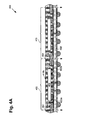
- Figure 4A presents structure 460 including testable semiconductor packages 400 and 470 prior to singulation, according to an implementation of the present disclosure.
- Figure 4B presents testable semiconductor package 400 (also referred to as "package 400") after being singulated from structure 460 along dicing lines 462 and 464.
- Package 400 corresponds to package 100 in Figure 1 .
- Figures 4A and 4B show active die 402, conductive mediums 406a and 406b, dedicated testing contacts 414a and 414b, top surface 416b, top surface 418b, and top metal layer segments 422a and 422e corresponding to active die 102, conductive mediums 106a and 106b, dedicated testing contacts 114a and 114b, top surface 116b, top surface 118b, and top metal layer segments 122a and 122e in Figure 1 .
- structure 460 includes conductive blocks 466a and 466b, which can be similar to copper blocks 234a and 234b in Figure 2 .
- conductive blocks 466a and 466b can comprise similar materials as conductive blocks 234a and 234b and can similarly be soldered respectively to top metal layer segments 422a and 422b. Molding 432 can subsequently be formed over conductive blocks 466a and 466b.
- conductive block 466b is connected to top metal layer segment 422e of package 400 and top metal layer segment 468 of testable semiconductor package 470, which can be similar to semiconductor package 400.
- Conductive blocks 466a and 466b are on sidewalls 472a and 472b of package 400 as shown in Figure 4B .
- Conductive medium 406a includes conductive block 466a and conductive medium 406b includes conductive block 466b.
- Figures 4A and 4B demonstrate one example where at least one conductive medium (e.g. conductive medium 406a) is providing electrical connection between at least one dedicated testing contact (e.g. dedicated testing contact 414a) and a sidewall (e.g. sidewall 472a) of a testable semiconductor package (e.g. testable semiconductor package 400).
- Figure 4A additionally includes conductive medium conductive medium 406b providing electrical connection between dedicated testing contact 414b and sidewall 472b of testable semiconductor package 400. It is noted that in some implementations, at least some of dedicated testing contacts 414 are on top surface 416b of active die 402 and are provided to sidewall 472a and/or sidewall 472b using, any suitable conductive medium, such as a copper block.
- package 400 can further include, for example, at least one conductive medium, instead of or in addition to conductive medium 406a, that is providing electrical connection between, for example, dedicated testing contact 414a and top surface 418b of package 400.
- the at least one conductive medium can be similar to or different than any of conductive mediums 106a, 206a, and 306a in Figures 1 , 2 , and 3 .
- Figure 4A and 4B offer an efficient example for fabricating package 400.
- package 400 can be fabricated many different ways and conductive mediums 406a and 406b are not limited by the implementation shown. In various implementations, package 400 can provide some similar advantages as described above with respect to packages 100, 200, and 300.
- Figure 5 presents system 580 for testing semiconductor package 500 (also referred to as "package 500"), according to an implementation of the present disclosure.
- System 580 includes package 500, top testing socket 582a and bottom testing socket 582b.
- Package 500 can correspond to any of previously described packages 100, 200, 300, and 400, and to packages not specifically described herein. In the implementation shown, package 500 most closely corresponds to package 100 in Figure 1 .
- Top testing socket 582a is electrically connected to dedicated testing contact 514a through conductive medium 506a for testing package 500.
- top testing socket 582a is electrically connected to dedicated testing contact 514a through package-top testing connection 508a, which is a solder ball.
- top testing socket 582a has top probes 584a and 584b for contacting package 500. More particularly, top probe 584a is connected to dedicated testing contact 514a and top probe 584b is connected to dedicated testing contact 514b.
- top probes 584a and 584b are pogo pins.
- Bottom testing socket 582b is connected to package-bottom connections 510.
- bottom testing socket 582b has bottom probes 586a, 586b, 586c, 586d, and 586e (also referred to collectively as "bottom probes 586") for contacting package 500.
- bottom probes 586 are pogo pins.
- at least some of bottom probes 586 are electrically connected to package-bottom connections 510 for testing package 500.
- at least some of bottom probes 586 are connected to package-bottom connections 510 only for structural support of package 500.
- each of package-bottom connections 510 is shown as having a corresponding bottom probe 586, in some implementations, at least one of package-bottom connections 510 is not directly contacting bottom testing socket 582b.
- bottom probe 586b could be removed. By doing so, there is less likelihood for damaging package-bottom connections 510 during testing of package 500.
- bottom probes 586 for respective interface contacts e.g. interface contact 512a
- package 500 does not include at least one of package-top testing connections 508 and top probes 584 can contact conductive mediums 506 directly. Similarly, in some implementations, package 500 does not include package-bottom connections 510. Furthermore, top probes 584 and/or bottom probes 586 can be adapted for implementations where at least one conductive medium is providing electrical connection between at least one dedicated testing contact and a sidewall of a testable semiconductor package (e.g. package 400).
Landscapes
- Testing Of Individual Semiconductor Devices (AREA)
- Measuring Leads Or Probes (AREA)
- Testing Or Measuring Of Semiconductors Or The Like (AREA)
Abstract
Description
- Testing occurs during or after manufacturing to ensure that semiconductor packages and dies are capable of meeting certain stringent operating requirements and standards. Exemplary tests that may be performed on a semiconductor package include various tests for active dies within the package, such as electrical signal timing tests, voltage and current level tests, at-speed tests, direct current tests, bum-in tests, room/cold tests, and hot sort tests. The semiconductor package would include at least one active die with interface contacts that are provided to a bottom surface of the semiconductor package. The interface contacts may be utilized for regular operation of the semiconductor package (i.e. operation out in the field). In addition to the interface contacts, the active die can include dedicated testing contacts that are also provided to the bottom surface of the semiconductor package. These dedicated testing contacts are utilized for testing, but not for regular operation of the semiconductor package.
- In order to test the semiconductor package, it may be electrically connected to a testing equipment or device. An exemplary testing equipment or device may include a bottom portion and a top portion, where the bottom portion may receive all of the interface contacts and the dedicated testing contacts of the semiconductor package and the top portion may be utilized to physically hold the semiconductor package onto the bottom portion of the testing equipment or device. The semiconductor package may then be tested and screened for stringent operating requirements and standards. Subsequently, the semiconductor package may be used in the field in regular operation.
- The present disclosure is directed to a semiconductor package with improved testability, substantially as shown in and/or described in connection with at least one of the figures, and as set forth more completely in the claims.
- According to an aspect, a testable semiconductor package comprises:
- an active die having interface contacts and dedicated testing contacts;
- an interposer situated adjacent a bottom surface of said active die, said interposer providing electrical connections between said interface contacts and a bottom surface of said testable semiconductor package;
- at least one conductive medium providing electrical connection between at least one of said dedicated testing contacts and a top surface of said testable semiconductor package.
- Advantageously, said at least one conductive medium is coupled to a package-top testing connection.
- Advantageously, said package-top testing connection comprises a solder ball.
- Advantageously, said at least one conductive medium comprises a conductive via.
- Advantageously, said at least one conductive medium comprises a conductive block.
- Advantageously, at least a portion of said at least one conductive medium is formed in an upper interposer.
- Advantageously, the testable semiconductor package further comprises at least one top metal layer segment providing electrical connection between at least one of said dedicated testing contacts and said at least one conductive medium.
- Advantageously, said interface contacts are electrically connected to package-bottom connections.
- Advantageously, said package-bottom connections comprise solder balls.
- Advantageously, the testable semiconductor package further comprises a molding that encloses said active die.
- According to an aspect, a testable semiconductor package comprises:
- an active die having interface contacts and dedicated testing contacts;
- an interposer situated adjacent a bottom surface of said active die, said interposer providing electrical connections between said interface contacts and a bottom surface of said testable semiconductor package;
- at least one conductive medium providing electrical connection between at least one of said dedicated testing contacts and a sidewall of said testable semiconductor package.
- Advantageously, said at least one conductive medium comprises a conductive block.
- Advantageously, the testable semiconductor package further comprises at least one top metal layer segment providing electrical connection between at least one of said dedicated testing contacts and said at least one conductive medium.
- Advantageously, the testable semiconductor package further comprises a molding that encloses said active die.
- According to an aspect, a system is provided for testing a semiconductor package, said system comprising:
- a semiconductor package comprising:
- an active die having interface contacts and dedicated testing contacts;
- an interposer situated adjacent a bottom surface of said active die, said interposer providing electrical connections between said interface contacts and a bottom surface of said semiconductor package;
- at least one conductive medium providing electrical connection between at least one of said dedicated testing contacts and a top surface of said semiconductor package;
- a top testing socket connected to said at least one of said dedicated testing contacts through said at least one conductive medium.
- Advantageously, said at least one conductive medium is coupled to a package-top testing connection.
- Advantageously, said top testing socket is connected to said at least one of said dedicated testing contacts through a solder ball.
- Advantageously, the system comprises a bottom testing socket connected to at least one package-bottom connection.
- Advantageously, at least one of said interface contacts is electrically connected to said package-bottom connection through said interposer.
- Advantageously, the system comprises a pogo pin connected to said at least one of said dedicated testing contacts.
-
-
Figure 1 presents an exemplary cross-sectional view of a testable semiconductor package, according to an implementation of the present disclosure. -
Figure 2 presents an exemplary cross-sectional view of a testable semiconductor package, according to an implementation of the present disclosure. -
Figure 3 presents an exemplary cross-sectional view of a testable semiconductor package, according to an implementation of the present disclosure. -
Figure 4A presents an exemplary cross-sectional view of testable semiconductor packages prior to singulation, according to an implementation of the present disclosure. -
Figure 4B presents an exemplary cross-sectional view of a testable semiconductor package after singulation, according to an implementation of the present disclosure. -
Figure 5 presents an exemplary cross-sectional view of a system for testing a semiconductor package, according to an implementation of the present disclosure. - The following description contains specific information pertaining to implementations in the present disclosure. One skilled in the art will recognize that the present disclosure may be implemented in a manner different from that specifically discussed herein. The drawings in the present application and their accompanying detailed description are directed to merely exemplary implementations. Unless noted otherwise, like or corresponding elements among the figures may be indicated by like or corresponding reference numerals. Moreover, the drawings and illustrations in the present application are generally not to scale, and are not intended to correspond to actual relative dimensions.
-
Figure 1 presents testable semiconductor package 100 (also referred to as "package 100"), according to an implementation of the present disclosure.Package 100 includes active die 102, interposer 104 (or more generally "substrate 104"),conductive mediums top testing connections bottom connections molding 132. - Active die 102 has
interface contacts dedicated testing contacts Active die 102 can include, for example, an integrated circuit (IC), and other electrical components that are connected to interface contacts 112 and dedicated testing contacts 114. As shown inFigure 1 , in the present implementation, at least some of interface contacts 112 and dedicated testing contacts 114 include solder balls (e.g. micro-bumps), as one example. Interface contacts 112 are utilized for regular operation ofpackage 100. In other words, interface contacts 112 are for regular operation out in the field. At least some of interface contacts 112 can have additional uses, such as fortesting package 100. However, dedicated testing contacts 114 are utilized for testing, but not for regular operation ofpackage 100. - While interface contacts 112 and dedicated testing contacts 114 are shown as being coupled to
bottom surface 116a ofactive die 102, any of interface contacts 112 and dedicated testing contacts 114 can be coupled to different surfaces ofactive die 102 includingtop surface 116b. In such implementations, interface contacts 112 and dedicated testing contacts 114 can include bond wires or other connection means. Also, while onlyactive die 102 is shown inFigure 1 ,package 100 includes additional active dies in some implementations. The additional dies can have additional interface contacts 112 and dedicated testing contacts 114. - In
package 100,interposer 104 is situatedadjacent bottom surface 116a ofactive die 102.Interposer 104 is providing electrical connections between interface contacts 112 andbottom surface 118a ofpackage 100. In the present implementation,interposer 104 includessubstrate core 120, topmetal layer segments top solder mask 124, bottommetal layer segments bottom solder mask 128, andvias -
Substrate 104 include, as examples, an organic-substrate, a laminate substrate, and a ceramic substrate. In thepresent implementation substrate 104 includes a laminate substrate.Substrate 104 is shown as having top metal layer segments 122 and bottom metal layer segments 126, but can include more than two layers of metal segments. - Also in
package 100, interface contacts 112 are electrically connected to package-bottom connections 110 throughinterposer 104. Package-bottom connections 110 are electrically connected to at least some of bottom metal layer segments 126. In the present implementation, at least some of package-bottom connections 110 are solder balls and can form a ball grid array (BGA). However,package 100 can include different types of package-bottom connections 110 or not include package-bottom connections 110 in various implementations. In the present implementation, package-bottom connections 110 are situated on at least some of bottom metal layer segments 126 through respective openings inbottom solder mask 128. It is noted thatinterposer 104 can have many different forms and is presented as one example. -
Package 100 further includes conductive mediums 106 providing electrical connection between dedicated testing contacts 114 andtop surface 118b ofpackage 100. For example, conductive medium 106a is providing electrical connection betweendedicated testing contact 114a andtop surface 118b and conductive medium 106b is providing electrical connection betweendedicated testing contact 114b andtop surface 118b. Thus, dedicated testing contacts 114 are available for testing ontop surface 118b ofpackage 100. - In some cases,
bottom surface 118a is considered highly valuable package area. For example, it may be desirable to provide all or most of interface contacts 112 tobottom surface 118a for regular operation ofpackage 100. As one example, it may be easier to deploypackage 100 out in the field. However, having dedicated testing contacts 114 provided tobottom surface 118a may, for example, hinder providing some of interface contacts 112 tobottom surface 118a. By providing dedicated testing contacts 114 totop surface 118b ofpackage 100 instead of tobottom surface 118a ofpackage 100, additional space can be created onbottom surface 118a for, for example, interface contacts 112 or for other purposes. As such, in some implementations, it may be easier to provide all or most of interface contacts 112 tobottom surface 118a for regular operation ofpackage 100. Furthermore, it may be possible to provide additional interface contacts 112 tobottom surface 118a, thereby enhancing functionality ofpackage 100. Additionally, it may be possible to reduce the overall footprint or package size ofpackage 100. - In the present implementation, top metal layer segments 122 are providing electrical connection between dedicated testing contacts 114 and conductive mediums 106. For example, top
metal layer segment 122a is providing electrical connection betweendedicated testing contact 114a and conductive medium 106a. Conductive mediums 106 are coupled to respective package-top testing connections 108. Package-top testing connections 108 are shown as being solder balls. However, some implementations do not include package-top testing connections 108 or include different types of package-top testing connections 108. - Also in the present implementation, conductive mediums 106 include through mold vias (TMVs) 105a and 105b (also referred to as "conductive via 105a" and "conductive via 105b") that are situated within
molding 132, which enclosesactive die 102. In the implementation shown, conductive mediums 106traverse bottom surface 116a andtop surface 116b ofactive die 102. Forming conductive mediums 106 can include, for example, forming vias throughmolding 132 andtop solder mask 124 and filling the vias with conductive material that can include, as examples, a metal or metal alloy to formTMVs top surface 118b, including directly overactive die 102. In some implementations, at least some of dedicated testing contacts 114 are ontop surface 116b ofactive die 102 and are provided totop surface 118b using, any suitable conductive medium, such as a TMV. - In various implementations,
package 100 can be, as examples, a fine ball grid array (FBGA) package, a flip chip (FC) package, a quad-flat no-leads (QFN) package, a top probe interposer package, a wafer level package, a package-on-package (PoP) type package, or other type of package not specifically described herein. While implementations shown herein includemolding 132, other implementations do not includemolding 132. Furthermore, conductive mediums 106 can take many different forms from what is shown inFigure 1 . As another example,Figure 2 presents testable semiconductor package 200 (also referred to as "package 200"), according to an implementation of the present disclosure. -
Package 200 corresponds to package 100 inFigure 1 . Thus, at least some similar and/or same elements betweenFigures 1 and2 are not specifically described with respect toFigure 2 .Package 200 includesactive die 202,conductive mediums dedicated testing contacts 214a and 214b,bottom surface 216a,top surface 216b,top surface 218b, topmetal layer segments molding 232 corresponding respectively toactive die 102,conductive mediums dedicated testing contacts bottom surface 116a,top surface 116b,top surface 118b, topmetal layer segments molding 132 inFigure 1 . - In
Figure 2 , conductive medium 206a includesconductive block 234a, which is attached to topmetal layer segment 222a usingsolder 236a. Similarly,conductive medium 206b includesconductive block 234b, which is attached to topmetal layer segment 222e usingsolder 236b.Conductive blocks implementation conductive blocks package 200 can include, for example, solderingconductive blocks metal layer segments molding 232 overconductive blocks dedicated testing contacts 214a and 214b) are ontop surface 216b ofactive die 202 and are provided totop surface 218b using, for example, a copper block. - As another example,
Figure 3 presents testable semiconductor package 300 (also referred to as "package 300"), according to an implementation of the present disclosure.Package 300 corresponds to package 100 inFigure 1 . Thus, at least some similar and/or same elements betweenFigures 1 and3 are not specifically described with respect toFigure 3 .Package 300 includesactive die 302, lower interposer 304 (or more generally "lower substrate 304"),conductive mediums top testing connections dedicated testing contacts bottom surface 316a,top surface 316b,top surface 318b, topmetal layer segments molding 332 corresponding respectively toactive die 102,interposer 104,conductive mediums top testing connections dedicated testing contacts bottom surface 116a,top surface 116b,top surface 118b, topmetal layer segments molding 132 inFigure 1 . -
Package 300 also includes upper interposer 340 (or more generally "upper substrate 340") situated adjacenttop surface 316b ofactive die 302.Upper interposer 340 can be, as examples, a silicon interposer, a laminate substrate, and the like. Asupper interposer 340 is a silicon interposer in the present implementation,upper interposer 340 includessubstrate core 342, topmetal layer segments metal layer segments vias Vias Upper interposer 340 can be a similar type of interposer or substrate aslower interposer 304 as shown inFigure 3 , or can be a different type of interposer or substrate aslower interposer 304. - In the implementation shown in
Figure 3 , at least a portion of conductive medium 306a is formed inupper interposer 340. Additionally, at least a portion of conductive medium 306b is formed inupper interposer 340. For example, conductive medium 306a includes topmetal layer segment 346a, bottommetal layer segment 350a, via 354a, andinterconnect solder ball 344a. Conductive medium 306b includes topmetal layer segment 346b, bottommetal layer segment 350b,vias interconnect solder ball 344b. Topmetal layer segments metal layer segments vias upper interposer 340. - In the implementation shown,
interconnect solder ball 344a is electrically connecting bottommetal layer segment 350a ofupper interposer 340 to topmetal layer segment 322a oflower interposer 304. Package-top testing connection 308a is situated on and electrically connected to topmetal layer segment 346a through an opening intop solder mask 348. Similarly,interconnect solder ball 344b is electrically connecting bottommetal layer segment 350b ofupper interposer 340 to topmetal layer segment 322e oflower interposer 304. Package-top testing connection 308b is situated on and electrically connected to topmetal layer segment 346b through an opening intop solder mask 348. By forming at least a portion ofconductive mediums upper interposer 340,package 300 can easily support robust routing capabilities for providingdedicated testing contacts top surface 318b. - Implementations described with respect to
Figures 1 ,2 , and3 show where at least one conductive medium is providing electrical connection between at least one dedicated testing contact and a top surface of a testable semiconductor package. Additionally, or instead, in some implementations, at least one conductive medium is providing electrical connection between at least one dedicated testing contact and a sidewall of a testable semiconductor package. For example,Figure 4A presentsstructure 460 includingtestable semiconductor packages Figure 4B presents testable semiconductor package 400 (also referred to as "package 400") after being singulated fromstructure 460 along dicinglines -
Package 400 corresponds to package 100 inFigure 1 . Thus, at least some similar and/or same elements betweenFigures 1 and4A and4B are not specifically described with respect toFigures 4A and4B .Figures 4A and4B showactive die 402,conductive mediums dedicated testing contacts top surface 416b,top surface 418b, and topmetal layer segments active die 102,conductive mediums dedicated testing contacts top surface 116b,top surface 118b, and topmetal layer segments Figure 1 . - As shown in
Figure 4A ,structure 460 includesconductive blocks copper blocks Figure 2 . Thus, for example,conductive blocks conductive blocks metal layer segments 422a and 422b. Molding 432 can subsequently be formed overconductive blocks Figure 4A ,conductive block 466b is connected to topmetal layer segment 422e ofpackage 400 and topmetal layer segment 468 oftestable semiconductor package 470, which can be similar tosemiconductor package 400. - After
singulating package 400 along dicinglines conductive blocks package 400 as shown inFigure 4B . Conductive medium 406a includesconductive block 466a and conductive medium 406b includesconductive block 466b. Thus,Figures 4A and4B demonstrate one example where at least one conductive medium (e.g. conductive medium 406a) is providing electrical connection between at least one dedicated testing contact (e.g.dedicated testing contact 414a) and a sidewall (e.g. sidewall 472a) of a testable semiconductor package (e.g. testable semiconductor package 400).Figure 4A additionally includes conductive medium conductive medium 406b providing electrical connection betweendedicated testing contact 414b andsidewall 472b oftestable semiconductor package 400. It is noted that in some implementations, at least some of dedicated testing contacts 414 are ontop surface 416b ofactive die 402 and are provided tosidewall 472a and/orsidewall 472b using, any suitable conductive medium, such as a copper block. - As discussed above,
package 400 can further include, for example, at least one conductive medium, instead of or in addition to conductive medium 406a, that is providing electrical connection between, for example,dedicated testing contact 414a andtop surface 418b ofpackage 400. In various implementations, the at least one conductive medium can be similar to or different than any ofconductive mediums Figures 1 ,2 , and3 . - Furthermore,
Figure 4A and4B offer an efficient example for fabricatingpackage 400. However,package 400 can be fabricated many different ways andconductive mediums package 400 can provide some similar advantages as described above with respect topackages - Referring now to
Figure 5, Figure 5 presentssystem 580 for testing semiconductor package 500 (also referred to as "package 500"), according to an implementation of the present disclosure.System 580 includespackage 500,top testing socket 582a andbottom testing socket 582b.Package 500 can correspond to any of previously describedpackages package 500 most closely corresponds to package 100 inFigure 1 . -
Top testing socket 582a is electrically connected todedicated testing contact 514a through conductive medium 506a fortesting package 500. In the implementation shown,top testing socket 582a is electrically connected todedicated testing contact 514a through package-top testing connection 508a, which is a solder ball. As shown inFigure 5 ,top testing socket 582a hastop probes package 500. More particularly,top probe 584a is connected todedicated testing contact 514a andtop probe 584b is connected to dedicated testing contact 514b. In the present implementation,top probes -
Bottom testing socket 582b is connected to package-bottom connections 510. As shown inFigure 5 ,bottom testing socket 582b hasbottom probes package 500. In the present implementation, bottom probes 586 are pogo pins. In some implementations, at least some of bottom probes 586 are electrically connected to package-bottom connections 510 fortesting package 500. In some implementations, at least some of bottom probes 586 are connected to package-bottom connections 510 only for structural support ofpackage 500. - Furthermore, while each of package-bottom connections 510 is shown as having a corresponding bottom probe 586, in some implementations, at least one of package-bottom connections 510 is not directly contacting
bottom testing socket 582b. For example,bottom probe 586b could be removed. By doing so, there is less likelihood for damaging package-bottom connections 510 during testing ofpackage 500. In particular, bottom probes 586 for respective interface contacts (e.g. interface contact 512a) that are not utilized for testing could be removed. - In some implementations,
package 500 does not include at least one of package-top testing connections 508 and top probes 584 can contact conductive mediums 506 directly. Similarly, in some implementations,package 500 does not include package-bottom connections 510. Furthermore, top probes 584 and/or bottom probes 586 can be adapted for implementations where at least one conductive medium is providing electrical connection between at least one dedicated testing contact and a sidewall of a testable semiconductor package (e.g. package 400). - From the above description it is manifest that various techniques can be used for implementing the concepts described in the present application without departing from the scope of those concepts. Moreover, while the concepts have been described with specific reference to certain implementations, a person of ordinary skill in the art would recognize that changes can be made in form and detail without departing from the spirit and the scope of those concepts. As such, the described implementations are to be considered in all respects as illustrative and not restrictive. It should also be understood that the present application is not limited to the particular implementations described herein, but many rearrangements, modifications, and substitutions are possible without departing from the scope of the present disclosure.
Claims (15)
- A testable semiconductor package comprising:an active die having interface contacts and dedicated testing contacts;an interposer situated adjacent a bottom surface of said active die, said interposer providing electrical connections between said interface contacts and a bottom surface of said testable semiconductor package;at least one conductive medium providing electrical connection between at least one of said dedicated testing contacts and a top surface of said testable semiconductor package.
- The testable semiconductor package of claim 1, wherein said at least one conductive medium is coupled to a package-top testing connection.
- The testable semiconductor package of claim 2, wherein said package-top testing connection comprises a solder ball.
- The testable semiconductor package of claim 1, wherein said at least one conductive medium comprises a conductive via.
- The testable semiconductor package of claim 1, wherein said at least one conductive medium comprises a conductive block.
- The testable semiconductor package of claim 1, wherein at least a portion of said at least one conductive medium is formed in an upper interposer.
- The testable semiconductor package of claim 1, comprising at least one top metal layer segment providing electrical connection between at least one of said dedicated testing contacts and said at least one conductive medium.
- The testable semiconductor package of claim 1, wherein said interface contacts are electrically connected to package-bottom connections.
- The testable semiconductor package of claim 8, wherein said package-bottom connections comprise solder balls.
- The testable semiconductor package of claim 1, comprising a molding that encloses said active die.
- A testable semiconductor package comprising:an active die having interface contacts and dedicated testing contacts;an interposer situated adjacent a bottom surface of said active die, said interposer providing electrical connections between said interface contacts and a bottom surface of said testable semiconductor package;at least one conductive medium providing electrical connection between at least one of said dedicated testing contacts and a sidewall of said testable semiconductor package.
- The testable semiconductor package of claim 11, wherein said at least one conductive medium comprises a conductive block.
- The testable semiconductor package of claim 11, comprising at least one top metal layer segment providing electrical connection between at least one of said dedicated testing contacts and said at least one conductive medium.
- The testable semiconductor package of claim 11, comprising a molding that encloses said active die.
- A system for testing a semiconductor package, said system comprising:a semiconductor package comprising:an active die having interface contacts and dedicated testing contacts;an interposer situated adjacent a bottom surface of said active die, said interposer providing electrical connections between said interface contacts and a bottom surface of said semiconductor package;at least one conductive medium providing electrical connection between at least one of said dedicated testing contacts and a top surface of said semiconductor package;a top testing socket connected to said at least one of said dedicated testing contacts through said at least one conductive medium.
Applications Claiming Priority (1)
| Application Number | Priority Date | Filing Date | Title |
|---|---|---|---|
| US13/362,344 US9153507B2 (en) | 2012-01-31 | 2012-01-31 | Semiconductor package with improved testability |
Publications (3)
| Publication Number | Publication Date |
|---|---|
| EP2624288A2 true EP2624288A2 (en) | 2013-08-07 |
| EP2624288A3 EP2624288A3 (en) | 2016-04-20 |
| EP2624288B1 EP2624288B1 (en) | 2019-08-21 |
Family
ID=46982327
Family Applications (1)
| Application Number | Title | Priority Date | Filing Date |
|---|---|---|---|
| EP12006188.2A Active EP2624288B1 (en) | 2012-01-31 | 2012-08-31 | Semiconductor package with improved testability |
Country Status (5)
| Country | Link |
|---|---|
| US (1) | US9153507B2 (en) |
| EP (1) | EP2624288B1 (en) |
| KR (1) | KR101356408B1 (en) |
| CN (2) | CN103227166B (en) |
| TW (1) | TWI497662B (en) |
Families Citing this family (11)
| Publication number | Priority date | Publication date | Assignee | Title |
|---|---|---|---|---|
| US9153507B2 (en) * | 2012-01-31 | 2015-10-06 | Broadcom Corporation | Semiconductor package with improved testability |
| CN104217967A (en) * | 2013-05-31 | 2014-12-17 | 宏启胜精密电子(秦皇岛)有限公司 | Semiconductor device and manufacturing method thereof |
| TW201514517A (en) * | 2013-10-11 | 2015-04-16 | Mpi Corp | Detection method of intermediate plate and intermediate plate adapted for the detection method |
| US9721852B2 (en) * | 2014-01-21 | 2017-08-01 | International Business Machines Corporation | Semiconductor TSV device package to which other semiconductor device package can be later attached |
| KR101622453B1 (en) | 2014-01-22 | 2016-05-31 | 앰코 테크놀로지 코리아 주식회사 | Semiconductor device and manufacturing method thereof |
| US20150340308A1 (en) * | 2014-05-21 | 2015-11-26 | Broadcom Corporation | Reconstituted interposer semiconductor package |
| KR101563909B1 (en) * | 2014-08-19 | 2015-10-28 | 앰코 테크놀로지 코리아 주식회사 | Method for manufacturing Package On Package |
| KR101573314B1 (en) | 2015-09-18 | 2015-12-02 | 앰코 테크놀로지 코리아 주식회사 | Package On Package |
| KR20230011643A (en) | 2021-07-14 | 2023-01-25 | 삼성전자주식회사 | Semiconductor packages having conneting stucture |
| TWI906166B (en) * | 2023-08-17 | 2025-11-21 | 南亞科技股份有限公司 | Method for measuring semiconductor package |
| TWI879027B (en) * | 2023-08-17 | 2025-04-01 | 南亞科技股份有限公司 | Semiconductor package |
Family Cites Families (21)
| Publication number | Priority date | Publication date | Assignee | Title |
|---|---|---|---|---|
| US5334857A (en) * | 1992-04-06 | 1994-08-02 | Motorola, Inc. | Semiconductor device with test-only contacts and method for making the same |
| DE59913490D1 (en) | 1998-06-16 | 2006-07-06 | Infineon Technologies Ag | DEVICE FOR MEASURING AND ANALYZING ELECTRICAL SIGNALS OF AN INTEGRATED CIRCUIT UNIT |
| DE10255378B4 (en) * | 2002-11-27 | 2006-03-23 | Advanced Micro Devices, Inc., Sunnyvale | Test structure for determining the stability of electronic devices comprising interconnected substrates |
| US6985645B2 (en) | 2003-09-24 | 2006-01-10 | International Business Machines Corporation | Apparatus and methods for integrally packaging optoelectronic devices, IC chips and optical transmission lines |
| US7838983B2 (en) * | 2005-04-26 | 2010-11-23 | Kyushu Institute Of Technology | Packaged semiconductor device and method of manufacturing the packaged semiconductor device |
| US20080002460A1 (en) * | 2006-03-01 | 2008-01-03 | Tessera, Inc. | Structure and method of making lidded chips |
| US7608921B2 (en) * | 2006-12-07 | 2009-10-27 | Stats Chippac, Inc. | Multi-layer semiconductor package |
| US7781235B2 (en) | 2006-12-21 | 2010-08-24 | Taiwan Semiconductor Manufacturing Company, Ltd. | Chip-probing and bumping solutions for stacked dies having through-silicon vias |
| CN100501991C (en) | 2007-06-29 | 2009-06-17 | 中兴通讯股份有限公司 | An encapsulated chip and its encapsulation method for chip |
| US8350382B2 (en) * | 2007-09-21 | 2013-01-08 | Infineon Technologies Ag | Semiconductor device including electronic component coupled to a backside of a chip |
| US20090108433A1 (en) * | 2007-10-30 | 2009-04-30 | Kenji Masumoto | Multilayer semiconductor device package assembly and method |
| US7808258B2 (en) | 2008-06-26 | 2010-10-05 | Freescale Semiconductor, Inc. | Test interposer having active circuit component and method therefor |
| JP4343256B1 (en) * | 2008-07-10 | 2009-10-14 | Necエレクトロニクス株式会社 | Manufacturing method of semiconductor device |
| WO2010010910A1 (en) | 2008-07-23 | 2010-01-28 | 日本電気株式会社 | Coreless wiring substrate, semiconductor device, and methods for manufacturing same |
| US7936060B2 (en) * | 2009-04-29 | 2011-05-03 | International Business Machines Corporation | Reworkable electronic device assembly and method |
| KR101086972B1 (en) | 2009-10-01 | 2011-11-29 | 앰코 테크놀로지 코리아 주식회사 | Wafer level package having through electrode and method for manufacturing same |
| KR101104352B1 (en) * | 2009-12-23 | 2012-01-16 | (주)솔리드메카 | How to fix the interposer PC for BA package test |
| KR20110088234A (en) * | 2010-01-28 | 2011-08-03 | 삼성전자주식회사 | Manufacturing method of laminated semiconductor package |
| KR101855294B1 (en) * | 2010-06-10 | 2018-05-08 | 삼성전자주식회사 | Semiconductor package |
| US8922230B2 (en) * | 2011-05-11 | 2014-12-30 | Taiwan Semiconductor Manufacturing Company, Ltd. | 3D IC testing apparatus |
| US9153507B2 (en) | 2012-01-31 | 2015-10-06 | Broadcom Corporation | Semiconductor package with improved testability |
-
2012
- 2012-01-31 US US13/362,344 patent/US9153507B2/en active Active
- 2012-08-31 EP EP12006188.2A patent/EP2624288B1/en active Active
- 2012-09-12 TW TW101133338A patent/TWI497662B/en not_active IP Right Cessation
- 2012-09-26 CN CN201210365269.0A patent/CN103227166B/en active Active
- 2012-09-26 CN CN2012204981629U patent/CN202816935U/en not_active Expired - Fee Related
- 2012-09-26 KR KR1020120106958A patent/KR101356408B1/en not_active Expired - Fee Related
Non-Patent Citations (1)
| Title |
|---|
| None |
Also Published As
| Publication number | Publication date |
|---|---|
| KR20130088717A (en) | 2013-08-08 |
| EP2624288A3 (en) | 2016-04-20 |
| TW201332069A (en) | 2013-08-01 |
| US9153507B2 (en) | 2015-10-06 |
| EP2624288B1 (en) | 2019-08-21 |
| KR101356408B1 (en) | 2014-01-27 |
| US20130193996A1 (en) | 2013-08-01 |
| CN202816935U (en) | 2013-03-20 |
| CN103227166B (en) | 2016-11-23 |
| TWI497662B (en) | 2015-08-21 |
| CN103227166A (en) | 2013-07-31 |
Similar Documents
| Publication | Publication Date | Title |
|---|---|---|
| EP2624288B1 (en) | Semiconductor package with improved testability | |
| CN110660754B (en) | Semiconductor package | |
| US12525544B2 (en) | Ultra small molded module integrated with die by module-on-wafer assembly | |
| US11508692B2 (en) | Package structure and method of fabricating the same | |
| US10074623B2 (en) | Method of fabricating redistribution circuit structure | |
| CN104851814B (en) | Ic package and forming method thereof | |
| US8643164B2 (en) | Package-on-package technology for fan-out wafer-level packaging | |
| US11244906B2 (en) | Semiconductor structure and method of fabricating the same | |
| KR20100029243A (en) | Semiconductor assemblies, stacked semiconductor devices, and methods of manufacturing semiconductor assemblies and stacked semiconductor devices | |
| US20090039508A1 (en) | Larger than die size wafer-level redistribution packaging process | |
| US20220336412A1 (en) | Package structure and method of fabricating the same | |
| US12463099B2 (en) | Semiconductor package including test line structure | |
| CN110875272A (en) | Semiconductor package and method of forming the same | |
| US20210351163A1 (en) | High density pillar interconnect conversion with stack to substrate connection | |
| US12519026B2 (en) | Semiconductor structure with capping member containing oxynitride layer and method of manufacturing thereof | |
| KR101332858B1 (en) | Device for array observation of multi-stack die | |
| US11631644B2 (en) | High density pillar interconnect conversion with stack to substrate connection | |
| CN222532096U (en) | Semiconductor device and semiconductor package | |
| US11018056B1 (en) | Encapsulated solder TSV insertion interconnect | |
| HK1185449A (en) | Semiconductor package with improved testability | |
| US20240170349A1 (en) | Semiconductor structure with testing pads and method of manufacturing thereof |
Legal Events
| Date | Code | Title | Description |
|---|---|---|---|
| PUAI | Public reference made under article 153(3) epc to a published international application that has entered the european phase |
Free format text: ORIGINAL CODE: 0009012 |
|
| 17P | Request for examination filed |
Effective date: 20120831 |
|
| AK | Designated contracting states |
Kind code of ref document: A2 Designated state(s): AL AT BE BG CH CY CZ DE DK EE ES FI FR GB GR HR HU IE IS IT LI LT LU LV MC MK MT NL NO PL PT RO RS SE SI SK SM TR |
|
| AX | Request for extension of the european patent |
Extension state: BA ME |
|
| RIN1 | Information on inventor provided before grant (corrected) |
Inventor name: KHAN, REZAUR Inventor name: KARIKALAN, SAMPATH Inventor name: HU, KEVIN Inventor name: VORENKAMP, PIETER Inventor name: CHEN, XIANGDONG Inventor name: ZHAO, SAM |
|
| PUAL | Search report despatched |
Free format text: ORIGINAL CODE: 0009013 |
|
| AK | Designated contracting states |
Kind code of ref document: A3 Designated state(s): AL AT BE BG CH CY CZ DE DK EE ES FI FR GB GR HR HU IE IS IT LI LT LU LV MC MK MT NL NO PL PT RO RS SE SI SK SM TR |
|
| AX | Request for extension of the european patent |
Extension state: BA ME |
|
| RIC1 | Information provided on ipc code assigned before grant |
Ipc: H01L 23/498 20060101ALI20160317BHEP Ipc: H01L 21/56 20060101ALI20160317BHEP Ipc: H01L 21/66 20060101AFI20160317BHEP Ipc: H01L 23/31 20060101ALI20160317BHEP |
|
| 17Q | First examination report despatched |
Effective date: 20160421 |
|
| RBV | Designated contracting states (corrected) |
Designated state(s): AL AT BE BG CH CY CZ DE DK EE ES FI FR GB GR HR HU IE IS IT LI LT LU LV MC MK MT NL NO PL PT RO RS SE SI SK SM TR |
|
| STAA | Information on the status of an ep patent application or granted ep patent |
Free format text: STATUS: EXAMINATION IS IN PROGRESS |
|
| RAP1 | Party data changed (applicant data changed or rights of an application transferred) |
Owner name: AVAGO TECHNOLOGIES GENERAL IP (SINGAPORE) PTE. LTD |
|
| RAP1 | Party data changed (applicant data changed or rights of an application transferred) |
Owner name: AVAGO TECHNOLOGIES INTERNATIONAL SALES PTE. LIMITE |
|
| GRAP | Despatch of communication of intention to grant a patent |
Free format text: ORIGINAL CODE: EPIDOSNIGR1 |
|
| STAA | Information on the status of an ep patent application or granted ep patent |
Free format text: STATUS: GRANT OF PATENT IS INTENDED |
|
| INTG | Intention to grant announced |
Effective date: 20190319 |
|
| GRAS | Grant fee paid |
Free format text: ORIGINAL CODE: EPIDOSNIGR3 |
|
| GRAA | (expected) grant |
Free format text: ORIGINAL CODE: 0009210 |
|
| STAA | Information on the status of an ep patent application or granted ep patent |
Free format text: STATUS: THE PATENT HAS BEEN GRANTED |
|
| AK | Designated contracting states |
Kind code of ref document: B1 Designated state(s): AL AT BE BG CH CY CZ DE DK EE ES FI FR GB GR HR HU IE IS IT LI LT LU LV MC MK MT NL NO PL PT RO RS SE SI SK SM TR |
|
| REG | Reference to a national code |
Ref country code: GB Ref legal event code: FG4D |
|
| REG | Reference to a national code |
Ref country code: CH Ref legal event code: EP |
|
| REG | Reference to a national code |
Ref country code: DE Ref legal event code: R096 Ref document number: 602012063060 Country of ref document: DE |
|
| REG | Reference to a national code |
Ref country code: AT Ref legal event code: REF Ref document number: 1170719 Country of ref document: AT Kind code of ref document: T Effective date: 20190915 |
|
| REG | Reference to a national code |
Ref country code: IE Ref legal event code: FG4D |
|
| REG | Reference to a national code |
Ref country code: LT Ref legal event code: MG4D |
|
| REG | Reference to a national code |
Ref country code: NL Ref legal event code: MP Effective date: 20190821 |
|
| PG25 | Lapsed in a contracting state [announced via postgrant information from national office to epo] |
Ref country code: LT Free format text: LAPSE BECAUSE OF FAILURE TO SUBMIT A TRANSLATION OF THE DESCRIPTION OR TO PAY THE FEE WITHIN THE PRESCRIBED TIME-LIMIT Effective date: 20190821 Ref country code: FI Free format text: LAPSE BECAUSE OF FAILURE TO SUBMIT A TRANSLATION OF THE DESCRIPTION OR TO PAY THE FEE WITHIN THE PRESCRIBED TIME-LIMIT Effective date: 20190821 Ref country code: SE Free format text: LAPSE BECAUSE OF FAILURE TO SUBMIT A TRANSLATION OF THE DESCRIPTION OR TO PAY THE FEE WITHIN THE PRESCRIBED TIME-LIMIT Effective date: 20190821 Ref country code: PT Free format text: LAPSE BECAUSE OF FAILURE TO SUBMIT A TRANSLATION OF THE DESCRIPTION OR TO PAY THE FEE WITHIN THE PRESCRIBED TIME-LIMIT Effective date: 20191223 Ref country code: HR Free format text: LAPSE BECAUSE OF FAILURE TO SUBMIT A TRANSLATION OF THE DESCRIPTION OR TO PAY THE FEE WITHIN THE PRESCRIBED TIME-LIMIT Effective date: 20190821 Ref country code: NO Free format text: LAPSE BECAUSE OF FAILURE TO SUBMIT A TRANSLATION OF THE DESCRIPTION OR TO PAY THE FEE WITHIN THE PRESCRIBED TIME-LIMIT Effective date: 20191121 Ref country code: BG Free format text: LAPSE BECAUSE OF FAILURE TO SUBMIT A TRANSLATION OF THE DESCRIPTION OR TO PAY THE FEE WITHIN THE PRESCRIBED TIME-LIMIT Effective date: 20191121 Ref country code: NL Free format text: LAPSE BECAUSE OF FAILURE TO SUBMIT A TRANSLATION OF THE DESCRIPTION OR TO PAY THE FEE WITHIN THE PRESCRIBED TIME-LIMIT Effective date: 20190821 |
|
| PG25 | Lapsed in a contracting state [announced via postgrant information from national office to epo] |
Ref country code: ES Free format text: LAPSE BECAUSE OF FAILURE TO SUBMIT A TRANSLATION OF THE DESCRIPTION OR TO PAY THE FEE WITHIN THE PRESCRIBED TIME-LIMIT Effective date: 20190821 Ref country code: AL Free format text: LAPSE BECAUSE OF FAILURE TO SUBMIT A TRANSLATION OF THE DESCRIPTION OR TO PAY THE FEE WITHIN THE PRESCRIBED TIME-LIMIT Effective date: 20190821 Ref country code: LV Free format text: LAPSE BECAUSE OF FAILURE TO SUBMIT A TRANSLATION OF THE DESCRIPTION OR TO PAY THE FEE WITHIN THE PRESCRIBED TIME-LIMIT Effective date: 20190821 Ref country code: IS Free format text: LAPSE BECAUSE OF FAILURE TO SUBMIT A TRANSLATION OF THE DESCRIPTION OR TO PAY THE FEE WITHIN THE PRESCRIBED TIME-LIMIT Effective date: 20191221 Ref country code: GR Free format text: LAPSE BECAUSE OF FAILURE TO SUBMIT A TRANSLATION OF THE DESCRIPTION OR TO PAY THE FEE WITHIN THE PRESCRIBED TIME-LIMIT Effective date: 20191122 Ref country code: RS Free format text: LAPSE BECAUSE OF FAILURE TO SUBMIT A TRANSLATION OF THE DESCRIPTION OR TO PAY THE FEE WITHIN THE PRESCRIBED TIME-LIMIT Effective date: 20190821 |
|
| REG | Reference to a national code |
Ref country code: AT Ref legal event code: MK05 Ref document number: 1170719 Country of ref document: AT Kind code of ref document: T Effective date: 20190821 |
|
| PG25 | Lapsed in a contracting state [announced via postgrant information from national office to epo] |
Ref country code: TR Free format text: LAPSE BECAUSE OF FAILURE TO SUBMIT A TRANSLATION OF THE DESCRIPTION OR TO PAY THE FEE WITHIN THE PRESCRIBED TIME-LIMIT Effective date: 20190821 |
|
| PG25 | Lapsed in a contracting state [announced via postgrant information from national office to epo] |
Ref country code: EE Free format text: LAPSE BECAUSE OF FAILURE TO SUBMIT A TRANSLATION OF THE DESCRIPTION OR TO PAY THE FEE WITHIN THE PRESCRIBED TIME-LIMIT Effective date: 20190821 Ref country code: DK Free format text: LAPSE BECAUSE OF FAILURE TO SUBMIT A TRANSLATION OF THE DESCRIPTION OR TO PAY THE FEE WITHIN THE PRESCRIBED TIME-LIMIT Effective date: 20190821 Ref country code: AT Free format text: LAPSE BECAUSE OF FAILURE TO SUBMIT A TRANSLATION OF THE DESCRIPTION OR TO PAY THE FEE WITHIN THE PRESCRIBED TIME-LIMIT Effective date: 20190821 Ref country code: PL Free format text: LAPSE BECAUSE OF FAILURE TO SUBMIT A TRANSLATION OF THE DESCRIPTION OR TO PAY THE FEE WITHIN THE PRESCRIBED TIME-LIMIT Effective date: 20190821 Ref country code: RO Free format text: LAPSE BECAUSE OF FAILURE TO SUBMIT A TRANSLATION OF THE DESCRIPTION OR TO PAY THE FEE WITHIN THE PRESCRIBED TIME-LIMIT Effective date: 20190821 Ref country code: IT Free format text: LAPSE BECAUSE OF FAILURE TO SUBMIT A TRANSLATION OF THE DESCRIPTION OR TO PAY THE FEE WITHIN THE PRESCRIBED TIME-LIMIT Effective date: 20190821 |
|
| PG25 | Lapsed in a contracting state [announced via postgrant information from national office to epo] |
Ref country code: SM Free format text: LAPSE BECAUSE OF FAILURE TO SUBMIT A TRANSLATION OF THE DESCRIPTION OR TO PAY THE FEE WITHIN THE PRESCRIBED TIME-LIMIT Effective date: 20190821 Ref country code: CH Free format text: LAPSE BECAUSE OF NON-PAYMENT OF DUE FEES Effective date: 20190831 Ref country code: SK Free format text: LAPSE BECAUSE OF FAILURE TO SUBMIT A TRANSLATION OF THE DESCRIPTION OR TO PAY THE FEE WITHIN THE PRESCRIBED TIME-LIMIT Effective date: 20190821 Ref country code: LI Free format text: LAPSE BECAUSE OF NON-PAYMENT OF DUE FEES Effective date: 20190831 Ref country code: LU Free format text: LAPSE BECAUSE OF NON-PAYMENT OF DUE FEES Effective date: 20190831 Ref country code: MC Free format text: LAPSE BECAUSE OF FAILURE TO SUBMIT A TRANSLATION OF THE DESCRIPTION OR TO PAY THE FEE WITHIN THE PRESCRIBED TIME-LIMIT Effective date: 20190821 Ref country code: IS Free format text: LAPSE BECAUSE OF FAILURE TO SUBMIT A TRANSLATION OF THE DESCRIPTION OR TO PAY THE FEE WITHIN THE PRESCRIBED TIME-LIMIT Effective date: 20200224 Ref country code: CZ Free format text: LAPSE BECAUSE OF FAILURE TO SUBMIT A TRANSLATION OF THE DESCRIPTION OR TO PAY THE FEE WITHIN THE PRESCRIBED TIME-LIMIT Effective date: 20190821 |
|
| REG | Reference to a national code |
Ref country code: BE Ref legal event code: MM Effective date: 20190831 |
|
| REG | Reference to a national code |
Ref country code: DE Ref legal event code: R097 Ref document number: 602012063060 Country of ref document: DE |
|
| PLBE | No opposition filed within time limit |
Free format text: ORIGINAL CODE: 0009261 |
|
| STAA | Information on the status of an ep patent application or granted ep patent |
Free format text: STATUS: NO OPPOSITION FILED WITHIN TIME LIMIT |
|
| PG2D | Information on lapse in contracting state deleted |
Ref country code: IS |
|
| PG25 | Lapsed in a contracting state [announced via postgrant information from national office to epo] |
Ref country code: IE Free format text: LAPSE BECAUSE OF NON-PAYMENT OF DUE FEES Effective date: 20190831 |
|
| 26N | No opposition filed |
Effective date: 20200603 |
|
| PG25 | Lapsed in a contracting state [announced via postgrant information from national office to epo] |
Ref country code: SI Free format text: LAPSE BECAUSE OF FAILURE TO SUBMIT A TRANSLATION OF THE DESCRIPTION OR TO PAY THE FEE WITHIN THE PRESCRIBED TIME-LIMIT Effective date: 20190821 Ref country code: BE Free format text: LAPSE BECAUSE OF NON-PAYMENT OF DUE FEES Effective date: 20190831 |
|
| GBPC | Gb: european patent ceased through non-payment of renewal fee |
Effective date: 20191121 |
|
| PG25 | Lapsed in a contracting state [announced via postgrant information from national office to epo] |
Ref country code: FR Free format text: LAPSE BECAUSE OF NON-PAYMENT OF DUE FEES Effective date: 20191021 Ref country code: GB Free format text: LAPSE BECAUSE OF NON-PAYMENT OF DUE FEES Effective date: 20191121 |
|
| PG25 | Lapsed in a contracting state [announced via postgrant information from national office to epo] |
Ref country code: CY Free format text: LAPSE BECAUSE OF FAILURE TO SUBMIT A TRANSLATION OF THE DESCRIPTION OR TO PAY THE FEE WITHIN THE PRESCRIBED TIME-LIMIT Effective date: 20190821 |
|
| PG25 | Lapsed in a contracting state [announced via postgrant information from national office to epo] |
Ref country code: MT Free format text: LAPSE BECAUSE OF FAILURE TO SUBMIT A TRANSLATION OF THE DESCRIPTION OR TO PAY THE FEE WITHIN THE PRESCRIBED TIME-LIMIT Effective date: 20190821 Ref country code: HU Free format text: LAPSE BECAUSE OF FAILURE TO SUBMIT A TRANSLATION OF THE DESCRIPTION OR TO PAY THE FEE WITHIN THE PRESCRIBED TIME-LIMIT; INVALID AB INITIO Effective date: 20120831 |
|
| PG25 | Lapsed in a contracting state [announced via postgrant information from national office to epo] |
Ref country code: MK Free format text: LAPSE BECAUSE OF FAILURE TO SUBMIT A TRANSLATION OF THE DESCRIPTION OR TO PAY THE FEE WITHIN THE PRESCRIBED TIME-LIMIT Effective date: 20190821 |
|
| PGFP | Annual fee paid to national office [announced via postgrant information from national office to epo] |
Ref country code: DE Payment date: 20250811 Year of fee payment: 14 |
|
| REG | Reference to a national code |
Ref country code: DE Ref legal event code: R079 Ref document number: 602012063060 Country of ref document: DE Free format text: PREVIOUS MAIN CLASS: H01L0021660000 Ipc: H10P0074000000 |