EP2621730B1 - Security element - Google Patents
Security element Download PDFInfo
- Publication number
- EP2621730B1 EP2621730B1 EP11760796.0A EP11760796A EP2621730B1 EP 2621730 B1 EP2621730 B1 EP 2621730B1 EP 11760796 A EP11760796 A EP 11760796A EP 2621730 B1 EP2621730 B1 EP 2621730B1
- Authority
- EP
- European Patent Office
- Prior art keywords
- layer
- low
- refraction
- medium
- index
- Prior art date
- Legal status (The legal status is an assumption and is not a legal conclusion. Google has not performed a legal analysis and makes no representation as to the accuracy of the status listed.)
- Active
Links
- 239000000463 material Substances 0.000 claims description 86
- 239000000758 substrate Substances 0.000 claims description 64
- 238000000034 method Methods 0.000 claims description 24
- 238000000151 deposition Methods 0.000 claims description 20
- 229920003229 poly(methyl methacrylate) Polymers 0.000 claims description 19
- 239000004926 polymethyl methacrylate Substances 0.000 claims description 19
- 238000004519 manufacturing process Methods 0.000 claims description 17
- 239000011159 matrix material Substances 0.000 claims description 17
- 229920003227 poly(N-vinyl carbazole) Polymers 0.000 claims description 17
- 230000008021 deposition Effects 0.000 claims description 15
- 229920000642 polymer Polymers 0.000 claims description 15
- 230000008569 process Effects 0.000 claims description 14
- 238000004049 embossing Methods 0.000 claims description 10
- 239000000975 dye Substances 0.000 claims description 9
- 239000004417 polycarbonate Substances 0.000 claims description 6
- 229920001577 copolymer Polymers 0.000 claims description 5
- 229910052751 metal Inorganic materials 0.000 claims description 5
- 239000002184 metal Substances 0.000 claims description 5
- 239000000020 Nitrocellulose Substances 0.000 claims description 3
- BZHJMEDXRYGGRV-UHFFFAOYSA-N Vinyl chloride Chemical compound ClC=C BZHJMEDXRYGGRV-UHFFFAOYSA-N 0.000 claims description 3
- 229920001109 fluorescent polymer Polymers 0.000 claims description 3
- PXZQEOJJUGGUIB-UHFFFAOYSA-N isoindolin-1-one Chemical class C1=CC=C2C(=O)NCC2=C1 PXZQEOJJUGGUIB-UHFFFAOYSA-N 0.000 claims description 3
- 229920001220 nitrocellulos Polymers 0.000 claims description 3
- 229920000515 polycarbonate Polymers 0.000 claims description 3
- NIXOWILDQLNWCW-UHFFFAOYSA-M Acrylate Chemical compound [O-]C(=O)C=C NIXOWILDQLNWCW-UHFFFAOYSA-M 0.000 claims description 2
- 239000010410 layer Substances 0.000 description 164
- 239000000203 mixture Substances 0.000 description 15
- -1 benzocoumarins Chemical class 0.000 description 13
- 239000000123 paper Substances 0.000 description 13
- 239000011248 coating agent Substances 0.000 description 11
- 238000000576 coating method Methods 0.000 description 11
- 239000004922 lacquer Substances 0.000 description 10
- WYURNTSHIVDZCO-UHFFFAOYSA-N Tetrahydrofuran Chemical compound C1CCOC1 WYURNTSHIVDZCO-UHFFFAOYSA-N 0.000 description 8
- 230000008859 change Effects 0.000 description 8
- 238000005286 illumination Methods 0.000 description 8
- 230000003287 optical effect Effects 0.000 description 8
- 239000012790 adhesive layer Substances 0.000 description 7
- 239000011888 foil Substances 0.000 description 7
- 230000005855 radiation Effects 0.000 description 7
- 238000010521 absorption reaction Methods 0.000 description 6
- MILUBEOXRNEUHS-UHFFFAOYSA-N iridium(3+) Chemical class [Ir+3] MILUBEOXRNEUHS-UHFFFAOYSA-N 0.000 description 6
- 239000002086 nanomaterial Substances 0.000 description 6
- 229920000742 Cotton Polymers 0.000 description 5
- 239000000853 adhesive Substances 0.000 description 5
- 230000001070 adhesive effect Effects 0.000 description 5
- 230000000694 effects Effects 0.000 description 5
- 239000002105 nanoparticle Substances 0.000 description 5
- 239000000243 solution Substances 0.000 description 5
- POILWHVDKZOXJZ-ARJAWSKDSA-M (z)-4-oxopent-2-en-2-olate Chemical compound C\C([O-])=C\C(C)=O POILWHVDKZOXJZ-ARJAWSKDSA-M 0.000 description 4
- CSCPPACGZOOCGX-UHFFFAOYSA-N Acetone Chemical compound CC(C)=O CSCPPACGZOOCGX-UHFFFAOYSA-N 0.000 description 4
- RTZKZFJDLAIYFH-UHFFFAOYSA-N Diethyl ether Chemical compound CCOCC RTZKZFJDLAIYFH-UHFFFAOYSA-N 0.000 description 4
- PXHVJJICTQNCMI-UHFFFAOYSA-N Nickel Chemical compound [Ni] PXHVJJICTQNCMI-UHFFFAOYSA-N 0.000 description 4
- 238000010894 electron beam technology Methods 0.000 description 4
- 239000000976 ink Substances 0.000 description 4
- 125000001997 phenyl group Chemical group [H]C1=C([H])C([H])=C(*)C([H])=C1[H] 0.000 description 4
- 239000004800 polyvinyl chloride Substances 0.000 description 4
- 229920000915 polyvinyl chloride Polymers 0.000 description 4
- 238000010791 quenching Methods 0.000 description 4
- YLQBMQCUIZJEEH-UHFFFAOYSA-N tetrahydrofuran Natural products C=1C=COC=1 YLQBMQCUIZJEEH-UHFFFAOYSA-N 0.000 description 4
- ZWEHNKRNPOVVGH-UHFFFAOYSA-N 2-Butanone Chemical compound CCC(C)=O ZWEHNKRNPOVVGH-UHFFFAOYSA-N 0.000 description 3
- XEKOWRVHYACXOJ-UHFFFAOYSA-N Ethyl acetate Chemical compound CCOC(C)=O XEKOWRVHYACXOJ-UHFFFAOYSA-N 0.000 description 3
- 108010043121 Green Fluorescent Proteins Proteins 0.000 description 3
- 239000011230 binding agent Substances 0.000 description 3
- 229920002678 cellulose Polymers 0.000 description 3
- 239000003086 colorant Substances 0.000 description 3
- 238000005516 engineering process Methods 0.000 description 3
- 230000005284 excitation Effects 0.000 description 3
- 239000010408 film Substances 0.000 description 3
- 239000011521 glass Substances 0.000 description 3
- 239000003446 ligand Substances 0.000 description 3
- 239000000178 monomer Substances 0.000 description 3
- 125000004430 oxygen atom Chemical group O* 0.000 description 3
- HRGDZIGMBDGFTC-UHFFFAOYSA-N platinum(2+) Chemical compound [Pt+2] HRGDZIGMBDGFTC-UHFFFAOYSA-N 0.000 description 3
- 229920000728 polyester Polymers 0.000 description 3
- 229920002451 polyvinyl alcohol Polymers 0.000 description 3
- 235000019422 polyvinyl alcohol Nutrition 0.000 description 3
- 238000007639 printing Methods 0.000 description 3
- 230000003595 spectral effect Effects 0.000 description 3
- 239000000126 substance Substances 0.000 description 3
- 125000006702 (C1-C18) alkyl group Chemical group 0.000 description 2
- LGXVIGDEPROXKC-UHFFFAOYSA-N 1,1-dichloroethene Chemical compound ClC(Cl)=C LGXVIGDEPROXKC-UHFFFAOYSA-N 0.000 description 2
- RNJVAUBBYGWVBF-UHFFFAOYSA-N 1-(2-prop-2-enoyloxypropoxy)propan-2-yl prop-2-enoate Chemical compound C=CC(=O)OC(C)COCC(C)OC(=O)C=C RNJVAUBBYGWVBF-UHFFFAOYSA-N 0.000 description 2
- ZDQNWDNMNKSMHI-UHFFFAOYSA-N 1-[2-(2-prop-2-enoyloxypropoxy)propoxy]propan-2-yl prop-2-enoate Chemical compound C=CC(=O)OC(C)COC(C)COCC(C)OC(=O)C=C ZDQNWDNMNKSMHI-UHFFFAOYSA-N 0.000 description 2
- VVZRKVYGKNFTRR-UHFFFAOYSA-N 12h-benzo[a]xanthene Chemical class C1=CC=CC2=C3CC4=CC=CC=C4OC3=CC=C21 VVZRKVYGKNFTRR-UHFFFAOYSA-N 0.000 description 2
- NIXOWILDQLNWCW-UHFFFAOYSA-N 2-Propenoic acid Natural products OC(=O)C=C NIXOWILDQLNWCW-UHFFFAOYSA-N 0.000 description 2
- ZAMLGGRVTAXBHI-UHFFFAOYSA-N 3-(4-bromophenyl)-3-[(2-methylpropan-2-yl)oxycarbonylamino]propanoic acid Chemical compound CC(C)(C)OC(=O)NC(CC(O)=O)C1=CC=C(Br)C=C1 ZAMLGGRVTAXBHI-UHFFFAOYSA-N 0.000 description 2
- BAPJBEWLBFYGME-UHFFFAOYSA-N Methyl acrylate Chemical compound COC(=O)C=C BAPJBEWLBFYGME-UHFFFAOYSA-N 0.000 description 2
- 229920003171 Poly (ethylene oxide) Polymers 0.000 description 2
- 239000004743 Polypropylene Substances 0.000 description 2
- 239000004372 Polyvinyl alcohol Substances 0.000 description 2
- 229920001131 Pulp (paper) Polymers 0.000 description 2
- VYPSYNLAJGMNEJ-UHFFFAOYSA-N Silicium dioxide Chemical compound O=[Si]=O VYPSYNLAJGMNEJ-UHFFFAOYSA-N 0.000 description 2
- GWEVSGVZZGPLCZ-UHFFFAOYSA-N Titan oxide Chemical compound O=[Ti]=O GWEVSGVZZGPLCZ-UHFFFAOYSA-N 0.000 description 2
- ZJCCRDAZUWHFQH-UHFFFAOYSA-N Trimethylolpropane Chemical compound CCC(CO)(CO)CO ZJCCRDAZUWHFQH-UHFFFAOYSA-N 0.000 description 2
- 239000007983 Tris buffer Substances 0.000 description 2
- MCMNRKCIXSYSNV-UHFFFAOYSA-N Zirconium dioxide Chemical compound O=[Zr]=O MCMNRKCIXSYSNV-UHFFFAOYSA-N 0.000 description 2
- 229940081735 acetylcellulose Drugs 0.000 description 2
- 150000001252 acrylic acid derivatives Chemical class 0.000 description 2
- 239000000654 additive Substances 0.000 description 2
- 239000004411 aluminium Substances 0.000 description 2
- 229910052782 aluminium Inorganic materials 0.000 description 2
- XAGFODPZIPBFFR-UHFFFAOYSA-N aluminium Chemical compound [Al] XAGFODPZIPBFFR-UHFFFAOYSA-N 0.000 description 2
- 239000005352 borofloat Substances 0.000 description 2
- 239000000969 carrier Substances 0.000 description 2
- 239000001913 cellulose Substances 0.000 description 2
- 229920002301 cellulose acetate Polymers 0.000 description 2
- XHXMPURWMSJENN-UHFFFAOYSA-N coumarin 480 Chemical compound C12=C3CCCN2CCCC1=CC1=C3OC(=O)C=C1C XHXMPURWMSJENN-UHFFFAOYSA-N 0.000 description 2
- 238000001723 curing Methods 0.000 description 2
- ZUOUZKKEUPVFJK-UHFFFAOYSA-N diphenyl Chemical compound C1=CC=CC=C1C1=CC=CC=C1 ZUOUZKKEUPVFJK-UHFFFAOYSA-N 0.000 description 2
- 239000006185 dispersion Substances 0.000 description 2
- 238000001035 drying Methods 0.000 description 2
- 238000005538 encapsulation Methods 0.000 description 2
- 239000004744 fabric Substances 0.000 description 2
- 230000003993 interaction Effects 0.000 description 2
- 229910052741 iridium Inorganic materials 0.000 description 2
- GKOZUEZYRPOHIO-UHFFFAOYSA-N iridium atom Chemical compound [Ir] GKOZUEZYRPOHIO-UHFFFAOYSA-N 0.000 description 2
- 239000010985 leather Substances 0.000 description 2
- 238000005259 measurement Methods 0.000 description 2
- 229920005615 natural polymer Polymers 0.000 description 2
- 229910052759 nickel Inorganic materials 0.000 description 2
- 239000002245 particle Substances 0.000 description 2
- 150000002979 perylenes Chemical class 0.000 description 2
- 238000000053 physical method Methods 0.000 description 2
- BASFCYQUMIYNBI-UHFFFAOYSA-N platinum Substances [Pt] BASFCYQUMIYNBI-UHFFFAOYSA-N 0.000 description 2
- 239000005020 polyethylene terephthalate Substances 0.000 description 2
- 229920000139 polyethylene terephthalate Polymers 0.000 description 2
- 229920000098 polyolefin Polymers 0.000 description 2
- 229920001155 polypropylene Polymers 0.000 description 2
- 239000004814 polyurethane Substances 0.000 description 2
- 229920002689 polyvinyl acetate Polymers 0.000 description 2
- 229920000036 polyvinylpyrrolidone Polymers 0.000 description 2
- 235000013855 polyvinylpyrrolidone Nutrition 0.000 description 2
- 230000000171 quenching effect Effects 0.000 description 2
- 238000000926 separation method Methods 0.000 description 2
- 238000001228 spectrum Methods 0.000 description 2
- 239000010409 thin film Substances 0.000 description 2
- 239000002023 wood Substances 0.000 description 2
- VEJOYRPGKZZTJW-FDGPNNRMSA-N (z)-4-hydroxypent-3-en-2-one;platinum Chemical compound [Pt].C\C(O)=C\C(C)=O.C\C(O)=C\C(C)=O VEJOYRPGKZZTJW-FDGPNNRMSA-N 0.000 description 1
- LHENQXAPVKABON-UHFFFAOYSA-N 1-methoxypropan-1-ol Chemical compound CCC(O)OC LHENQXAPVKABON-UHFFFAOYSA-N 0.000 description 1
- YOSZEPWSVKKQOV-UHFFFAOYSA-N 12h-benzo[a]phenoxazine Chemical class C1=CC=CC2=C3NC4=CC=CC=C4OC3=CC=C21 YOSZEPWSVKKQOV-UHFFFAOYSA-N 0.000 description 1
- BDDQPKXDNUKVCC-UHFFFAOYSA-N 12h-benzo[b]phenoxazine Chemical class C1=CC=C2C=C3NC4=CC=CC=C4OC3=CC2=C1 BDDQPKXDNUKVCC-UHFFFAOYSA-N 0.000 description 1
- SWAGSGUXOCHFHN-UHFFFAOYSA-N 12h-benzo[b]xanthene Chemical class C1=CC=C2C=C3CC4=CC=CC=C4OC3=CC2=C1 SWAGSGUXOCHFHN-UHFFFAOYSA-N 0.000 description 1
- VFMUXPQZKOKPOF-UHFFFAOYSA-N 2,3,7,8,12,13,17,18-octaethyl-21,23-dihydroporphyrin platinum Chemical compound [Pt].CCc1c(CC)c2cc3[nH]c(cc4nc(cc5[nH]c(cc1n2)c(CC)c5CC)c(CC)c4CC)c(CC)c3CC VFMUXPQZKOKPOF-UHFFFAOYSA-N 0.000 description 1
- SMZOUWXMTYCWNB-UHFFFAOYSA-N 2-(2-methoxy-5-methylphenyl)ethanamine Chemical compound COC1=CC=C(C)C=C1CCN SMZOUWXMTYCWNB-UHFFFAOYSA-N 0.000 description 1
- JAHNSTQSQJOJLO-UHFFFAOYSA-N 2-(3-fluorophenyl)-1h-imidazole Chemical compound FC1=CC=CC(C=2NC=CN=2)=C1 JAHNSTQSQJOJLO-UHFFFAOYSA-N 0.000 description 1
- WADCPEMKIBAJHH-UHFFFAOYSA-N 3,4-diphenylpyrrole-2,5-dione Chemical class O=C1NC(=O)C(C=2C=CC=CC=2)=C1C1=CC=CC=C1 WADCPEMKIBAJHH-UHFFFAOYSA-N 0.000 description 1
- DCPGBPKLXYETTA-UHFFFAOYSA-N 3-methylphenanthro[9,10-b]pyrazine Chemical compound C1=CC=C2C3=NC(C)=CN=C3C3=CC=CC=C3C2=C1 DCPGBPKLXYETTA-UHFFFAOYSA-N 0.000 description 1
- HQQTZCPKNZVLFF-UHFFFAOYSA-N 4h-1,2-benzoxazin-3-one Chemical class C1=CC=C2ONC(=O)CC2=C1 HQQTZCPKNZVLFF-UHFFFAOYSA-N 0.000 description 1
- HUKPVYBUJRAUAG-UHFFFAOYSA-N 7-benzo[a]phenalenone Chemical class C1=CC(C(=O)C=2C3=CC=CC=2)=C2C3=CC=CC2=C1 HUKPVYBUJRAUAG-UHFFFAOYSA-N 0.000 description 1
- VDISGEKPIVMONQ-UHFFFAOYSA-N 7h-benzo[c]phenoxazine Chemical class C1=CC2=CC=CC=C2C2=C1NC1=CC=CC=C1O2 VDISGEKPIVMONQ-UHFFFAOYSA-N 0.000 description 1
- RGHINSLFCBMCFS-UHFFFAOYSA-N 7h-benzo[c]xanthene Chemical class C1=CC2=CC=CC=C2C2=C1CC1=CC=CC=C1O2 RGHINSLFCBMCFS-UHFFFAOYSA-N 0.000 description 1
- QTBSBXVTEAMEQO-UHFFFAOYSA-M Acetate Chemical compound CC([O-])=O QTBSBXVTEAMEQO-UHFFFAOYSA-M 0.000 description 1
- HRPVXLWXLXDGHG-UHFFFAOYSA-N Acrylamide Chemical compound NC(=O)C=C HRPVXLWXLXDGHG-UHFFFAOYSA-N 0.000 description 1
- NLHHRLWOUZZQLW-UHFFFAOYSA-N Acrylonitrile Chemical compound C=CC#N NLHHRLWOUZZQLW-UHFFFAOYSA-N 0.000 description 1
- 229910002706 AlOOH Inorganic materials 0.000 description 1
- 229920002799 BoPET Polymers 0.000 description 1
- FERIUCNNQQJTOY-UHFFFAOYSA-M Butyrate Chemical compound CCCC([O-])=O FERIUCNNQQJTOY-UHFFFAOYSA-M 0.000 description 1
- FERIUCNNQQJTOY-UHFFFAOYSA-N Butyric acid Natural products CCCC(O)=O FERIUCNNQQJTOY-UHFFFAOYSA-N 0.000 description 1
- 229920002134 Carboxymethyl cellulose Polymers 0.000 description 1
- DQEFEBPAPFSJLV-UHFFFAOYSA-N Cellulose propionate Chemical compound CCC(=O)OCC1OC(OC(=O)CC)C(OC(=O)CC)C(OC(=O)CC)C1OC1C(OC(=O)CC)C(OC(=O)CC)C(OC(=O)CC)C(COC(=O)CC)O1 DQEFEBPAPFSJLV-UHFFFAOYSA-N 0.000 description 1
- 229920002284 Cellulose triacetate Polymers 0.000 description 1
- 239000001828 Gelatine Substances 0.000 description 1
- 239000004354 Hydroxyethyl cellulose Substances 0.000 description 1
- 229920000663 Hydroxyethyl cellulose Polymers 0.000 description 1
- 239000005041 Mylar™ Substances 0.000 description 1
- 241000208125 Nicotiana Species 0.000 description 1
- 235000002637 Nicotiana tabacum Nutrition 0.000 description 1
- 239000004677 Nylon Substances 0.000 description 1
- 239000004952 Polyamide Substances 0.000 description 1
- 239000004698 Polyethylene Substances 0.000 description 1
- 239000004642 Polyimide Substances 0.000 description 1
- 239000004793 Polystyrene Substances 0.000 description 1
- 241000220317 Rosa Species 0.000 description 1
- 229920000516 Self-adhesive stamp Polymers 0.000 description 1
- XUIMIQQOPSSXEZ-UHFFFAOYSA-N Silicon Chemical compound [Si] XUIMIQQOPSSXEZ-UHFFFAOYSA-N 0.000 description 1
- 238000003848 UV Light-Curing Methods 0.000 description 1
- XTXRWKRVRITETP-UHFFFAOYSA-N Vinyl acetate Chemical compound CC(=O)OC=C XTXRWKRVRITETP-UHFFFAOYSA-N 0.000 description 1
- NNLVGZFZQQXQNW-ADJNRHBOSA-N [(2r,3r,4s,5r,6s)-4,5-diacetyloxy-3-[(2s,3r,4s,5r,6r)-3,4,5-triacetyloxy-6-(acetyloxymethyl)oxan-2-yl]oxy-6-[(2r,3r,4s,5r,6s)-4,5,6-triacetyloxy-2-(acetyloxymethyl)oxan-3-yl]oxyoxan-2-yl]methyl acetate Chemical compound O([C@@H]1O[C@@H]([C@H]([C@H](OC(C)=O)[C@H]1OC(C)=O)O[C@H]1[C@@H]([C@@H](OC(C)=O)[C@H](OC(C)=O)[C@@H](COC(C)=O)O1)OC(C)=O)COC(=O)C)[C@@H]1[C@@H](COC(C)=O)O[C@@H](OC(C)=O)[C@H](OC(C)=O)[C@H]1OC(C)=O NNLVGZFZQQXQNW-ADJNRHBOSA-N 0.000 description 1
- GCPWJFKTWGFEHH-UHFFFAOYSA-N acetoacetamide Chemical class CC(=O)CC(N)=O GCPWJFKTWGFEHH-UHFFFAOYSA-N 0.000 description 1
- CUJRVFIICFDLGR-UHFFFAOYSA-N acetylacetonate Chemical compound CC(=O)[CH-]C(C)=O CUJRVFIICFDLGR-UHFFFAOYSA-N 0.000 description 1
- 239000002390 adhesive tape Substances 0.000 description 1
- 238000005054 agglomeration Methods 0.000 description 1
- 230000002776 aggregation Effects 0.000 description 1
- PNEYBMLMFCGWSK-UHFFFAOYSA-N aluminium oxide Inorganic materials [O-2].[O-2].[O-2].[Al+3].[Al+3] PNEYBMLMFCGWSK-UHFFFAOYSA-N 0.000 description 1
- 238000005452 bending Methods 0.000 description 1
- ZYGHJZDHTFUPRJ-UHFFFAOYSA-N benzo-alpha-pyrone Natural products C1=CC=C2OC(=O)C=CC2=C1 ZYGHJZDHTFUPRJ-UHFFFAOYSA-N 0.000 description 1
- 125000003354 benzotriazolyl group Chemical class N1N=NC2=C1C=CC=C2* 0.000 description 1
- 230000008033 biological extinction Effects 0.000 description 1
- 230000005540 biological transmission Effects 0.000 description 1
- 230000015572 biosynthetic process Effects 0.000 description 1
- 235000010290 biphenyl Nutrition 0.000 description 1
- 239000004305 biphenyl Substances 0.000 description 1
- 239000007767 bonding agent Substances 0.000 description 1
- 239000001768 carboxy methyl cellulose Substances 0.000 description 1
- 235000010948 carboxy methyl cellulose Nutrition 0.000 description 1
- 239000008112 carboxymethyl-cellulose Substances 0.000 description 1
- 239000003054 catalyst Substances 0.000 description 1
- 229920006218 cellulose propionate Polymers 0.000 description 1
- 238000006243 chemical reaction Methods 0.000 description 1
- 239000003795 chemical substances by application Substances 0.000 description 1
- 229910052681 coesite Inorganic materials 0.000 description 1
- 150000001875 compounds Chemical class 0.000 description 1
- 238000003851 corona treatment Methods 0.000 description 1
- 230000002596 correlated effect Effects 0.000 description 1
- 230000000875 corresponding effect Effects 0.000 description 1
- 229910052593 corundum Inorganic materials 0.000 description 1
- 235000001671 coumarin Nutrition 0.000 description 1
- 125000000332 coumarinyl group Chemical class O1C(=O)C(=CC2=CC=CC=C12)* 0.000 description 1
- 229910052906 cristobalite Inorganic materials 0.000 description 1
- 230000006378 damage Effects 0.000 description 1
- 238000013016 damping Methods 0.000 description 1
- 150000004826 dibenzofurans Chemical class 0.000 description 1
- 238000009826 distribution Methods 0.000 description 1
- 230000007613 environmental effect Effects 0.000 description 1
- 229940093499 ethyl acetate Drugs 0.000 description 1
- 235000019439 ethyl acetate Nutrition 0.000 description 1
- 239000000945 filler Substances 0.000 description 1
- 229920002457 flexible plastic Polymers 0.000 description 1
- 229920005570 flexible polymer Polymers 0.000 description 1
- 239000007850 fluorescent dye Substances 0.000 description 1
- 229920000159 gelatin Polymers 0.000 description 1
- 235000019322 gelatine Nutrition 0.000 description 1
- 230000009477 glass transition Effects 0.000 description 1
- 238000007646 gravure printing Methods 0.000 description 1
- 125000000623 heterocyclic group Chemical group 0.000 description 1
- 235000019447 hydroxyethyl cellulose Nutrition 0.000 description 1
- 238000003384 imaging method Methods 0.000 description 1
- HUVCZKYUWFGVLS-UHFFFAOYSA-N imidazo[4,5-e]thiazine Chemical class C1=NSC2=NC=NC2=C1 HUVCZKYUWFGVLS-UHFFFAOYSA-N 0.000 description 1
- 239000006115 industrial coating Substances 0.000 description 1
- 239000011229 interlayer Substances 0.000 description 1
- 238000002372 labelling Methods 0.000 description 1
- 238000003475 lamination Methods 0.000 description 1
- 229910052747 lanthanoid Inorganic materials 0.000 description 1
- 150000002602 lanthanoids Chemical class 0.000 description 1
- 230000001795 light effect Effects 0.000 description 1
- 150000002734 metacrylic acid derivatives Chemical class 0.000 description 1
- 125000001434 methanylylidene group Chemical group [H]C#[*] 0.000 description 1
- LVHBHZANLOWSRM-UHFFFAOYSA-N methylenebutanedioic acid Natural products OC(=O)CC(=C)C(O)=O LVHBHZANLOWSRM-UHFFFAOYSA-N 0.000 description 1
- 229910052754 neon Inorganic materials 0.000 description 1
- GKAOGPIIYCISHV-UHFFFAOYSA-N neon atom Chemical compound [Ne] GKAOGPIIYCISHV-UHFFFAOYSA-N 0.000 description 1
- 229920001778 nylon Polymers 0.000 description 1
- 150000004893 oxazines Chemical class 0.000 description 1
- 150000002991 phenoxazines Chemical class 0.000 description 1
- 238000005424 photoluminescence Methods 0.000 description 1
- 238000000103 photoluminescence spectrum Methods 0.000 description 1
- 239000012994 photoredox catalyst Substances 0.000 description 1
- 125000005543 phthalimide group Chemical class 0.000 description 1
- SIOXPEMLGUPBBT-UHFFFAOYSA-M picolinate Chemical compound [O-]C(=O)C1=CC=CC=N1 SIOXPEMLGUPBBT-UHFFFAOYSA-M 0.000 description 1
- 238000009832 plasma treatment Methods 0.000 description 1
- 229920003023 plastic Polymers 0.000 description 1
- 239000004033 plastic Substances 0.000 description 1
- 229920002647 polyamide Polymers 0.000 description 1
- 229920000570 polyether Polymers 0.000 description 1
- 229920000573 polyethylene Polymers 0.000 description 1
- 229920001721 polyimide Polymers 0.000 description 1
- 238000006116 polymerization reaction Methods 0.000 description 1
- 229920002223 polystyrene Polymers 0.000 description 1
- 229920002635 polyurethane Polymers 0.000 description 1
- 239000011118 polyvinyl acetate Substances 0.000 description 1
- 239000001267 polyvinylpyrrolidone Substances 0.000 description 1
- 239000011148 porous material Substances 0.000 description 1
- 150000004032 porphyrins Chemical class 0.000 description 1
- 230000003449 preventive effect Effects 0.000 description 1
- 239000011253 protective coating Substances 0.000 description 1
- 239000011241 protective layer Substances 0.000 description 1
- 150000003216 pyrazines Chemical class 0.000 description 1
- 150000003230 pyrimidines Chemical class 0.000 description 1
- 238000010526 radical polymerization reaction Methods 0.000 description 1
- 230000004044 response Effects 0.000 description 1
- 229910052710 silicon Inorganic materials 0.000 description 1
- 239000010703 silicon Substances 0.000 description 1
- 239000000377 silicon dioxide Substances 0.000 description 1
- 239000007787 solid Substances 0.000 description 1
- 239000002904 solvent Substances 0.000 description 1
- 238000004528 spin coating Methods 0.000 description 1
- 229910052682 stishovite Inorganic materials 0.000 description 1
- 238000006467 substitution reaction Methods 0.000 description 1
- 229920001059 synthetic polymer Polymers 0.000 description 1
- 229920001897 terpolymer Polymers 0.000 description 1
- 229920001169 thermoplastic Polymers 0.000 description 1
- 150000004897 thiazines Chemical class 0.000 description 1
- 125000001544 thienyl group Chemical group 0.000 description 1
- ILJSQTXMGCGYMG-UHFFFAOYSA-N triacetic acid Chemical compound CC(=O)CC(=O)CC(O)=O ILJSQTXMGCGYMG-UHFFFAOYSA-N 0.000 description 1
- 150000003918 triazines Chemical class 0.000 description 1
- 150000003852 triazoles Chemical class 0.000 description 1
- 229910052905 tridymite Inorganic materials 0.000 description 1
- 230000000007 visual effect Effects 0.000 description 1
- XLYOFNOQVPJJNP-UHFFFAOYSA-N water Substances O XLYOFNOQVPJJNP-UHFFFAOYSA-N 0.000 description 1
- 229920003169 water-soluble polymer Polymers 0.000 description 1
- 239000000080 wetting agent Substances 0.000 description 1
- 125000001834 xanthenyl group Chemical class C1=CC=CC=2OC3=CC=CC=C3C(C12)* 0.000 description 1
- 229910001845 yogo sapphire Inorganic materials 0.000 description 1
Images




Classifications
-
- B—PERFORMING OPERATIONS; TRANSPORTING
- B41—PRINTING; LINING MACHINES; TYPEWRITERS; STAMPS
- B41M—PRINTING, DUPLICATING, MARKING, OR COPYING PROCESSES; COLOUR PRINTING
- B41M3/00—Printing processes to produce particular kinds of printed work, e.g. patterns
- B41M3/14—Security printing
-
- G—PHYSICS
- G03—PHOTOGRAPHY; CINEMATOGRAPHY; ANALOGOUS TECHNIQUES USING WAVES OTHER THAN OPTICAL WAVES; ELECTROGRAPHY; HOLOGRAPHY
- G03H—HOLOGRAPHIC PROCESSES OR APPARATUS
- G03H1/00—Holographic processes or apparatus using light, infrared or ultraviolet waves for obtaining holograms or for obtaining an image from them; Details peculiar thereto
- G03H1/0005—Adaptation of holography to specific applications
- G03H1/0011—Adaptation of holography to specific applications for security or authentication
-
- B—PERFORMING OPERATIONS; TRANSPORTING
- B41—PRINTING; LINING MACHINES; TYPEWRITERS; STAMPS
- B41M—PRINTING, DUPLICATING, MARKING, OR COPYING PROCESSES; COLOUR PRINTING
- B41M3/00—Printing processes to produce particular kinds of printed work, e.g. patterns
- B41M3/14—Security printing
- B41M3/144—Security printing using fluorescent, luminescent or iridescent effects
-
- B—PERFORMING OPERATIONS; TRANSPORTING
- B42—BOOKBINDING; ALBUMS; FILES; SPECIAL PRINTED MATTER
- B42D—BOOKS; BOOK COVERS; LOOSE LEAVES; PRINTED MATTER CHARACTERISED BY IDENTIFICATION OR SECURITY FEATURES; PRINTED MATTER OF SPECIAL FORMAT OR STYLE NOT OTHERWISE PROVIDED FOR; DEVICES FOR USE THEREWITH AND NOT OTHERWISE PROVIDED FOR; MOVABLE-STRIP WRITING OR READING APPARATUS
- B42D15/00—Printed matter of special format or style not otherwise provided for
-
- B—PERFORMING OPERATIONS; TRANSPORTING
- B42—BOOKBINDING; ALBUMS; FILES; SPECIAL PRINTED MATTER
- B42D—BOOKS; BOOK COVERS; LOOSE LEAVES; PRINTED MATTER CHARACTERISED BY IDENTIFICATION OR SECURITY FEATURES; PRINTED MATTER OF SPECIAL FORMAT OR STYLE NOT OTHERWISE PROVIDED FOR; DEVICES FOR USE THEREWITH AND NOT OTHERWISE PROVIDED FOR; MOVABLE-STRIP WRITING OR READING APPARATUS
- B42D25/00—Information-bearing cards or sheet-like structures characterised by identification or security features; Manufacture thereof
- B42D25/20—Information-bearing cards or sheet-like structures characterised by identification or security features; Manufacture thereof characterised by a particular use or purpose
- B42D25/29—Securities; Bank notes
-
- B—PERFORMING OPERATIONS; TRANSPORTING
- B42—BOOKBINDING; ALBUMS; FILES; SPECIAL PRINTED MATTER
- B42D—BOOKS; BOOK COVERS; LOOSE LEAVES; PRINTED MATTER CHARACTERISED BY IDENTIFICATION OR SECURITY FEATURES; PRINTED MATTER OF SPECIAL FORMAT OR STYLE NOT OTHERWISE PROVIDED FOR; DEVICES FOR USE THEREWITH AND NOT OTHERWISE PROVIDED FOR; MOVABLE-STRIP WRITING OR READING APPARATUS
- B42D25/00—Information-bearing cards or sheet-like structures characterised by identification or security features; Manufacture thereof
- B42D25/30—Identification or security features, e.g. for preventing forgery
- B42D25/36—Identification or security features, e.g. for preventing forgery comprising special materials
- B42D25/373—Metallic materials
-
- B—PERFORMING OPERATIONS; TRANSPORTING
- B42—BOOKBINDING; ALBUMS; FILES; SPECIAL PRINTED MATTER
- B42D—BOOKS; BOOK COVERS; LOOSE LEAVES; PRINTED MATTER CHARACTERISED BY IDENTIFICATION OR SECURITY FEATURES; PRINTED MATTER OF SPECIAL FORMAT OR STYLE NOT OTHERWISE PROVIDED FOR; DEVICES FOR USE THEREWITH AND NOT OTHERWISE PROVIDED FOR; MOVABLE-STRIP WRITING OR READING APPARATUS
- B42D25/00—Information-bearing cards or sheet-like structures characterised by identification or security features; Manufacture thereof
- B42D25/30—Identification or security features, e.g. for preventing forgery
- B42D25/36—Identification or security features, e.g. for preventing forgery comprising special materials
- B42D25/378—Special inks
- B42D25/387—Special inks absorbing or reflecting ultraviolet light
-
- G—PHYSICS
- G03—PHOTOGRAPHY; CINEMATOGRAPHY; ANALOGOUS TECHNIQUES USING WAVES OTHER THAN OPTICAL WAVES; ELECTROGRAPHY; HOLOGRAPHY
- G03H—HOLOGRAPHIC PROCESSES OR APPARATUS
- G03H1/00—Holographic processes or apparatus using light, infrared or ultraviolet waves for obtaining holograms or for obtaining an image from them; Details peculiar thereto
- G03H1/02—Details of features involved during the holographic process; Replication of holograms without interference recording
- G03H1/024—Hologram nature or properties
- G03H1/0244—Surface relief holograms
-
- B42D2033/04—
-
- B—PERFORMING OPERATIONS; TRANSPORTING
- B42—BOOKBINDING; ALBUMS; FILES; SPECIAL PRINTED MATTER
- B42D—BOOKS; BOOK COVERS; LOOSE LEAVES; PRINTED MATTER CHARACTERISED BY IDENTIFICATION OR SECURITY FEATURES; PRINTED MATTER OF SPECIAL FORMAT OR STYLE NOT OTHERWISE PROVIDED FOR; DEVICES FOR USE THEREWITH AND NOT OTHERWISE PROVIDED FOR; MOVABLE-STRIP WRITING OR READING APPARATUS
- B42D25/00—Information-bearing cards or sheet-like structures characterised by identification or security features; Manufacture thereof
- B42D25/30—Identification or security features, e.g. for preventing forgery
- B42D25/328—Diffraction gratings; Holograms
-
- G—PHYSICS
- G03—PHOTOGRAPHY; CINEMATOGRAPHY; ANALOGOUS TECHNIQUES USING WAVES OTHER THAN OPTICAL WAVES; ELECTROGRAPHY; HOLOGRAPHY
- G03H—HOLOGRAPHIC PROCESSES OR APPARATUS
- G03H2222/00—Light sources or light beam properties
- G03H2222/10—Spectral composition
- G03H2222/15—Ultra Violet [UV]
-
- G—PHYSICS
- G03—PHOTOGRAPHY; CINEMATOGRAPHY; ANALOGOUS TECHNIQUES USING WAVES OTHER THAN OPTICAL WAVES; ELECTROGRAPHY; HOLOGRAPHY
- G03H—HOLOGRAPHIC PROCESSES OR APPARATUS
- G03H2240/00—Hologram nature or properties
- G03H2240/50—Parameters or numerical values associated with holography, e.g. peel strength
- G03H2240/54—Refractive index
Definitions
- the present invention is in the field of security documents, more particularly in the field of security elements aimed to protect security documents against copying (illegal reproduction) and counterfeiting. It discloses a security element having a security feature which changes its visual appearance after irradiation with light, especially with UV light and at rotation and/or tilting. Security documents comprising said security element, as well as a method for producing said security element, are also disclosed.
- EP1998193A1 describes a sensor adapted to be either one of fluorescing or phosphorescing, said sensor comprising: a zero-order diffractive filter for polarised or unpolarised polychromatic light, said zero-order diffractive filter comprising:
- the interface constituting nanostructures contains the fluorescing and phosphorescing material.
- This sensor reflects visible light in the zeroth order and shows a colour. This colour changes when the fluorescing or phosphorescing material reacts with the environment.To avoid damping of the light guided in the waveguiding layer the fluorescing or phosphorescing material is not included in the waveguiding layer.
- the method for manufacturing the sensor comprising the steps:
- WO2006018232A1 relates to a security element with an optically variable structure, comprising an embossed structure and a coating, whereby the embossed structure and the coating are combined such that at least part of the coating is fully visible when viewed perpendicularly but hidden on angled viewing.
- the embossed structure comprises non-linear embossed elements which are combined with the coating such that, on changing viewing angle, different information is visible.
- the coating may comprise luminescent materials.
- the coating is arranged on the embossed elements of the embossed structure.
- JP2003248414A relates to a wavelength hologram type forgery preventive seal having an input means for converting the external light made incident from the top surface of a plane type optical waveguide into waveguide light and output means formed with a hologram to generate diffracted light when the waveguide light is made incident thereon, is fixed with a transparent cover seal having an adhesive part to the surface of an object.
- the incoupling and outcoupling are not separated from eatch other. Both processes take place all over the grated area.
- EP1776242A1 relates to a security device composing a zero-order diffractive microstructure buried within a substrate and a further structure comprising one or more optical structures formed on a surface of the substrate to be viewed by a user that modifies the optical characteristics produced by the zero-order microstructure.
- One or more further optical structures such as microlenses 1 or sawtooth (20, fig 2 ), may be formed on a surface 2 of the substrate (3).
- the further optical structures modify the optical characteristics of the zero order diffractive microstructures 5.
- a material with a colour filter function may be added between the surface of the device 34 and the microstructures 33. Chromophores 31 may be added to the polymer 32.
- the device may be combined with a hologram.
- the chromphores materials with colour filter function, including fluorophors, phosphorescent dyes, nano-partcle like Q-Dots or metallic nano-partcles
- the colour filter modifies the spectra of the incident light as well as of the reflected light at the microstructures.
- EP0420261A2 ( EP1241022 ) relates to a system consisting of a series of data carriers, particularly identity cards, value papers or the like, in which the data carriers belonging to the system exhibit defraction structures which contain a standard information in which parts of the series are changed by additional measures in the area of the defraction structures, or combined with other elements and are visually recognisably distinguished from the rest of the series, the change in defraction structures and/or the combination with other elements conveying an overall aesthetic impression and the change and/or combination with the other elements not being cancellable without destruction of the defraction structures.
- the great number of possible variations include the use of different printing techniques, dyes, inks and metalized layers to produce certain optical impressions and realize special forms of individualization.
- the use of luminescent or phosphorescent substances may make special individualizing measures recognizable only in special illumination.
- an information recording part 6 laminated on a base material 2 is formed in the laminate structure comprising a peeling layer 61, a light- refracting structure layer 62, the light-reflective layer 63, a fluorescent layer 64, and an adhesive layer 65 from the top.
- At least one layer or interlayer region in the hologram structural layers including these layers contains an organic fluorescent dye, which is excited by IR rays and emits light in the IR region.
- the hologram of JP2001255808 provided with at least a hologram forming layer 2 and reflection thin-film layer 3 on a supporting layer 1 is characterized in that the fluorescent dyestuffs excited by UV rays to emit light in an IR region is contained in at least one layer among hologram constituting layers including the respective layers described above or between the layers.
- an image 3 such as a face photo or the like, is formed on a substrate 2, on which a first information pattern unit 14, containing fluorescence agent emitting infrared rays, is formed, while second information pattern units 15 are formed between either one of an image receiving layer 4 or a hologram layer 8 and a separable protective layer 5 to constitute an image indicating body.
- the information pattern units, provided in the image indicating body become luminous by the irradiation of infrared rays and ultraviolet rays, having specified wave lengths, whereby the information patterns can be confirmed visually.
- EP 2130884A1 discloses tamper resistant security labels or adhesive tapes comprising a flexible carrier substrate based on flexible plastic foil, where on the carrier substrate following labels are applied: (a) partially a release lacquer in the form of alphabetic characters, signs, symbols, lines, guilloche patterns, numbers or writings; (b) a full-faced or partial coating made from luminescent colors; (c) optionally one or more other layers having optical characteristics or metallic layers; (d) a self- adhesive coating or heat-seal lacquer coating.
- the carrier substrate exhibits an optically active structure, like diffractive structures, holograms or waves.
- the partial luminescent coating is present in the form of alphabetic characters, signs, symbols, lines, guilloche patterns, numbers or writings.
- JP2004223975A and JP2007072188A both disclose security devices associating UV hologram and fluorescence.
- the present invention aims to create an improved (printable) security feature combining UV hologram with fluorescence in a single system.
- Security feature should not be observable in ambient light but visible under excitation of, for example, 365 nm UV light.
- logo should switch contrast if tilted in the plane of the security feature and/or rotated about the surface normal.
- a security device as claimed in claim 1, comprising:
- Fig.1a shows a schematic top view of a security feature according to this invention.
- the security feature is illustrated as illuminated under day light conditions, e.g. sun light or neon lamp illumination.
- day light conditions e.g. sun light or neon lamp illumination.
- UV light illumination is shown.
- the logo is only visible under UV light illumination (in this case by UV light of LED with a peak at 365 nm).
- Fig. 1b shows schematically a contrast change of the security element at turning around normal.
- the UV hologram shows a contrast change at rotation on 90° around a normal to surface.
- Left image has green fluorescent abbreviation "BASF” surrounded by darker fluorescent background.
- BASF abbreviation
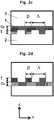
- Fig. 2a to 2d depict side view drawings of possible layer and microstructure setups for security features according to this invention.
- the letter p denotes the width of one bar of the shown diffraction microstructure, A is the period and t the depth of this diffractive microstructure and c h is the thickness of the homogeneous part of the waveguiding layer comprising the light emitting - respectively fluorescent or phosphorescent - material.
- Fig. 3 is a plot of the measured emission intensity versus wavelength at a viewing angle of 60° for Example 1 of this invention.
- the emission intensity was measured for one emitting material embedded in two different matrix materials of the waveguiding layer, namely PVK and PMMA. Further it was measured for the two different orientations of the used linear diffraction grating, namely viewing direction horizontal or vertical to grating lines.
- Fig. 4a shows schematically a contrast change of the security element at turning around normal.
- the UV hologram shows a contrast change at rotation on 90° around a normal to surface.
- Left image has green fluorescent abbreviation "BASF” surrounded by darker background.
- Turn of UV hologram on 90° changes color arrangement (dark abbreviation "BASF” is surrounded by green fluorescent background).
- BASF dark abbreviation
- Figure 4b shows a similar security element but with a flurescent image showing a rose instead oft he BASF letters.
- the fluorescent image changes from positive to negative image upon rotation.
- a grating coated by a waveguiding layer comprising a luminescent or light emitting material.
- the waveguiding layer is deposited first and microstructured with the grating afterwards.
- the waveguiding layer having a high refractive index and a resonance filter property of high reflection at appointed wavelength, groove orientation and illumination angle. High reflection at excitation wavelength provides an emission of luminescent material.
- Fig. 1 shows schematically the invisible in day light but visible in UV light effect
- Fig. 2 shows schematically side views of the layer and structure setup.
- the security device according to the present invention can be used in the manufacturing of banknotes, credit cards, passports, tickets and for brand protection purposes.
- the present invention is also directed to a product, such as, for example, a banknote, a credit card, a passport, or a ticket, comprising the security device according to the present invention.
- diffractive microstructure on the surface of the waveguiding layer means that the diffractive microstructure is embossed in the waveguiding layer.
- diffractive microstructure at the interface between the medium, or substrate and the waveguiding layer means that the diffractive microstructure is either embossed in the medium, or substrate; or the waveguiding layer. That means, the diffractive microstructure is part of the medium, or substrate; or the waveguiding layer.
- a waveguiding layer has at least one diffractive microstructure in one of its surface or one of its interface. Further the refractive index in spectral range of peak absorption of the light emitting material is typically at least 0.005 higher when compared with the adjacent layers. Many fluorescent or phosphorescent materials have a absorption peak in the UV spectral range. Advantegously the waveguiding layer is substantially transparent at least in part of the visible light. Preferred it has sharp interfaces to the adjacent layer(s) or media.
- Substantially transparent are layers with a transmission T>50%, preferably T>90%; at least in a part of the visible spectral range.
- a sharp interface according to this invention is less than 200 nm thick, preferred less than 80 nm thick, particularly preferred less than 30 nm thick.
- the interface is the zone between two layers where the refractive index changes from the value of one layer to the value of the other layer.
- the waveguiding layer has one diffractive microstructure in one of its surfaces.
- the period is preferably between 200 nm and 500 nm.
- the microstructures are linear, or crossed gratings.
- the term 'grating lines' is known in the field.
- the shape of the grating lines defines the microstructure.
- linear lines are used.
- the total mass thickness d of the waveguiding layer is preferably in the range between 80 nm and 200 nm.
- the waveguiding layer as described herein may comprise additional components, such as fillers, wetting agents and the like. Such additives are known in the field and are commercially available.
- Suitable parameters for the microstructured waveguiding layer according to this invention are summarized below: Parameter Preferred range Period ⁇ 200 - 500nm Mass thickness d 80 - 200nm depth t 100 - 300nm Fill factor f.f. 0.4 - 0.6 Thickness of Interface ⁇ 30 nm Thickness of separation layer c sep ⁇ 50 nm
- a high refractive index of a layer refers to the fact that the adjacent layers have a lower refractive index; and vice versa. Further, it is understood that, in line with physical principles, the minimum refractive index is 1.0. Thus, reference to a refractive index of e.g. "lower than 1.5" always implies "lower than 1.5 but at least 1.0".
- the diffractive microstructure is preferably a diffraction grating having a microstructure period ( ⁇ ) in the range of 270 ⁇ 30 nm; the thickness (d) of the waveguiding layer is in the range of 140 ⁇ 50 nm; and the microstructure depth (t) in the range of 140 ⁇ 30 nm.
- the diffractive microstructure consists of at least two part-areas adjacent or nearby to one another, wherein one part-area comprises one groves orientation and the other part-area comprises another different groves orientation and/or one part-area comprises one grating period and the other part-area comprises another different grating period.
- both part-areas comprise a logo in the diffractive microstructure, upon irradiation of the luminescent material the first logo appears bright and the second logo appears dark depending on the orientation of the groves and upon rotation the first logo appears dark and the second logo appears bright.
- the part-areas have preferably a defined shape, such as, for example, a symbol, a stripe, a geometrical shape, a design, lettering, an alphanumeric character, the representation of an object or parts thereof. Reference is made to Fig. 4 .
- Fig. 2a to Fig. 2d depict side view drawings of possible layer and microstructure setups for security features according to this invention.
- the letter p denotes the width of one bar of the shown diffraction microstructure, ⁇ is the period and t the depth of this diffractive microstructure and c h is the thickness of the homogeneous part of the waveguiding layer comprising the light emitting - respectively fluorescent or phosphorescent - material.
- the security devices shown in Fig. 2a and 2b consist of a medium, or substrate having a low index of refraction n low (2) and a waveguiding layer (1).
- the diffractive microstructure is at the interface between the medium, or substrate having a low index of refraction n low (2) and the waveguiding layer (1).
- the diffractive microstructure is on the surface of the waveguiding layer (1).
- the security devices shown in Fig. 2c and 2d consist of a medium, or substrate having a low index of refraction n low (2), a waveguiding layer (1) and a second medium having a low index of refraction n low (3).
- the diffractive microstructure is at the interface between the medium, or substrate having a low index of refraction n low (2) and the waveguiding layer (1).
- the diffractive microstructure is on the surface of the waveguiding layer (1).
- the luminescent material can solely constitute the waveguiding layer.
- the waveguiding layer having a high index of refraction n high comprises a matrix material and the luminescent material (light emitting material).
- the luminescent material is used in an amount of 0.1 to 40 % by weight, especially 0.1 to 20 % by weight, based on the amount of luminescent material and a matrix material.
- the waveguiding layer comprises a luminescent material.
- the luminescent material can solely constitute the waveguiding layer or represents one component of the waveguiding layer.
- the waveguiding layer may be made from a matrix plus light emitting material blend.
- the matrix material are polymers such as polymethylmethacrylate, or polyvinylcarbazole.
- the matrix material can be any material provided it has in combination with the luminescent a higher index of refraction than the medium having a low index of refraction n low .
- the matrix material include the materials mentioned below for the medium having a low index of refraction n low .
- the matrix can be UV primer (UV curable composition), or a water soluble, thermoplastic polymer.
- suitable water soluble polymers are selected from the group consisting of unmodified natural polymers, modified natural polymers, and synthetic polymers, including partly or completely hydrolyzed polyvinyl alcohol PVA and co-polymers with vinyl acetate and other monomers; modified polyvinyl alcohols; homo- or co-polymers of (meth)acrylamide; polyethylene oxide PEO; polyvinyl pyrrolidone PVP; polyvinylacetate; stark; cellulose and its derivatives, like hydroxyethylcellulose or carboxymethylcellulose; gelatine; polyurethane PU.
- unmodified natural polymers modified natural polymers, and synthetic polymers, including partly or completely hydrolyzed polyvinyl alcohol PVA and co-polymers with vinyl acetate and other monomers; modified polyvinyl alcohols; homo- or co-polymers of (meth)acrylamide; polyethylene oxide PEO; polyvinyl pyrrolidone PVP; polyvinylacetate; stark; cellulose and its derivatives, like
- the at present most preferred matrix materials are selected from polyvinylcarbazole, polymethylmethacrylate, UV primer (UV curable composition), vinyl chloride and vinyl acetate copolymers and nitrocellulose.
- the waveguiding layer comprises - besides the matrix and the light emitting material - nanoparticles with a refractive index that is higher than the one of the matrix material.
- examples are TiO 2 and ZrO 2 nanoparticles.
- the size of the nanoparticles is in the range of 5 nm to 200 nm, particularly preferred between 10 nm and 60 nm.
- the particle size distribution should preferably be low.
- the luminescent material can be any material which emits light in the visible, range after irradiation.
- the luminescent or light emitting material can be a fluorescent material, a phosphorescent material, or other like materials.
- Such luminescent materials exhibit a characteristic emission of electromagnetic energy in response to an energy source generally without any substantial rise in temperature.
- the luminescent material is irradiated at 365 nm (invisible irradiation) and shows visible emission.
- the luminescent material is a material which has an absorption maximum close to 365 nm (365 ⁇ 40 nm).
- the luminescent material may be selected from metal complexes, fluorescent organic dyes, fluorescent polymers, and inorganic phosphors.
- Metal complexes such as, for example phosphorescent materials may be used as luminescent material.
- phosphorescent and related materials are described, for example, in WO00/57676 , WO00/70655 , WO01/41512 , WO02/15645 , US2003/0017361 , WO01/93642 , WO01/39234 , US6,458,475 , WO02/071813 , US6,573,651 , US2002/0197511 , WO02/074015 , US6,451,455 , US2003/0072964 , US2003/0068528 , US6,413,656 , 6,515,298 , 6,451,415 , 6,097,147 , US2003/0124381 , US2003/0059646 , US2003/0054198 , EP1239526 , EP1238981 , EP1244155 , US2002/0100906 , US2003/0068526
- the emission wavelengths of cyclometallated Ir(III) complexes of the type IrL 3 and IrL 2 L' may be shifted by substitution of electron donating or withdrawing groups at appropriate positions on the cyclometallating ligand L, or by choice of different heterocycles for the cyclometallating ligand L.
- the emission wavelengths may also be shifted by choice of the ancillary ligand L'.
- red emitters examples include the bis(2-(2'-benzothienyl)pyridinato-N,C 3' )iridium(El)(acetylacetonate), iridium(III)bis(2methyldibenzo[f,h]quinoxaline) (acetylacetonate), and tris(1-phenylisoquinolinato-N,C)iridium(III).
- a blue-emitting example is bis(2-(4,6-difluorophenyl)-pyridinato-N,C 2' )Iridium(III)(picolinate).
- Red phosphorescence has been reported, using bis(2-(2'-benzo[4,5-a]thienyl)pyridinato-N, C 3 )iridium(acetylacetonate)[Btp 2 Ir(acac)] as the phosphorescent material ( Adachi, C., Lamansky, S., Baldo, M. A., Kwong, R. C., Thompson, M. E., and Forrest, S. R., App. Phys. Lett., 78, 1622 1624 (2001 ). Green phosphorescence has been reported for [ADS066GE).
- phosphorescent materials include cyclometallated Pt(II) complexes such as cis-bis(2-phenylpyridinato-N,C 2' )platinum(II), cis-bis(2-(2'-thienyl)pyridinato-N,C 3' ) platinum(II), cis-bis(2-(2'-thienyl)quinolinato-N,C 5' ) platinum(II), or (2-(4,6-diflourophenyl)pyridinato-NC2') platinum(II)acetylacetonate.
- Pt(II)porphyrin complexes such as 2,3,7,8,12,13,17,18-octaethyl-21H, 23H-porphine platinum(H) are also useful phosphorescent materials.
- phosphorescent materials are described in WO06/000544 and WO08/101842 , WO2005/019373 , WO2006/056418 , WO2005/113704 , WO2007/115970 , WO2007/115981 and WO2008/000727 .
- Still other examples of useful phosphorescent materials include coordination complexes of the trivalent lanthanides such as Th 3+ and Eu 3+ ( J. Kido et al, Appl. Phys. Lett., 65, 2124 (1994 ) and J. Kido et al, Chem. Rev.
- R 21 and R 22 are independently of each other H, phenyl, C 1 -C 18 alkyl, which may be interrupted by one, or more oxygen atoms, and R 22 and R 23 are independently of each other C 1 -C 18 alkyl, phenyl, which may be substituted by one, or more C 1 -C 18 alkyl groups, which may be interrupted by one, or more oxygen atoms; or biphenyl, which may be substituted by one, or more C 1 -C 18 alkyl groups, which may be interrupted by one, or more oxygen atoms.
- Suitable fluorescent colorants are based on known colorants selected from coumarins, benzoxazinones, benzocoumarins, xanthenes, benzo[a]xanthenes, benzo[b]xanthenes, benzo[c]xanthenes, phenoxazines, benzo[a]phenoxazines, benzo[b]phenoxazines and benzo[c]phenoxazines, napthalimides, naphtholactams, azlactones, methines, oxazines and thiazines, diketopyrrolopyrroles, perylenes, quinacridones, benzoxanthenes, thio-epindolines, lactamimides, diphenylmaleimides, acetoacetamides, imidazothiazines, benzanthrones, perylenmonoimides, perylenes, phthalimides, benzotriazoles, pyrimidine
- Figure 3 shows the corresponding fluorescence emission intensity versus wavelength spectra at an observation angle of 60° and for viewing direction vertical or horizontal to the grating lines.
- a fluorescent material with higher refractive index has better waveguiding property which leads to a higher emission intensity.
- Emission intensity can be increased with amount of emitter in waveguiding layer and/or excitation power.
- the diffractive microstructure is typically provided in a low index substrate before depositing the waveguiding layer. Alternatively it is applied to the waveguiding layer, for example by embossing.
- the layer of a medium having a low index of refraction n low can represent the substrate layer.
- the layer of a medium having a low index of refraction n low may be made from PET, PC, PMMA, or acrylates.
- the medium having a low index of refraction n low is preferably selected from polymethylmethacrylate, polycarbonate, polyethylenetherephatalate coated with an embossable layer, especially an embossable acrylate
- the layer of a medium having a low index of refraction n low may be made of an UV-curable polymer, such as Ormocomp® made by Micro Resist Technology, or the UV curable compositions described in WO2008/061930 (page 8 to 35).
- an UV-curable polymer such as Ormocomp® made by Micro Resist Technology, or the UV curable compositions described in WO2008/061930 (page 8 to 35).
- the layer of a medium having a low index of refraction n low can be a porous layer.
- porous layers are known in the art. They advantageously comprise inorganic nanoparticles, preferably in combination with one or more organic binders. Suitable inorganic nanoparticles are preferably selected from the group consisting of oxides like SiO 2 , Al 2 O 3 or AlOOH.
- the substrate of the security element can be made of any suitable material known to the skilled person.
- the selection of the substrate depends on the intended use and the manufacturing process.
- Substrates may e.g. be made of glass, paper, or polymer foils.
- transparent and flexible polymer foils are used.
- Such foils can be selected from the group consisting of Cellulose esters (like Cellulosetriacetate, Celluloseacetate, Cellulosepropionate or Celluloseacetate/butyrate), Polyesters (like Polyethylen terephthalate PET or Polyethylen naphthalate PEN), Polyamides, Polycarbonates PC, Polymethylmetacrylates PMMA, Polyimides PI, Polyolefins, Polyvinylacetates, Polyethers, Polyvinylchloride PVC and Polyvinylsulfone PSU.
- Preferred are Polyesters, particularly Polyethylenterephthalate like Mylar (DuPont) or Polyethylennaphthalate, due to their exceptional stability.
- Suitable opaque flexible substrates are for example Polyolefin coated paper and white opaque Polyester like Melinex (DuPont).
- the refractive index of the substrate at a wavelength of about 300 to 500 nm can e.g. be in the range of 1.35 to 1.80, but typically it is between 1.49 (PMMA) and 1.59 (PC).
- the thickness of the substrate depends on the intended use, and on the equipment used; it is preferably between 25 ⁇ m and 200 ⁇ m.
- the substrate is "flexible"; this relates to the bending properties, in particular to enable a roll-to-roll process for manufacturing a security element.
- the adhesion properties of the substrate may be improved by chemical or physical methods.
- Chemical methods include the deposition of a bonding agent, e.g. deposition of terpolymers of vinylidenchloride, acrylnitril and acrylic acid or of vinylidenchloride, methylacrylate and itaconic acid.
- Physical methods include plasma treatment like corona treatment.
- the substrates described above are commercially available or obtainable according to known methods.
- the security element according to the invention may comprise one or more covering layers, deposited on top of the waveguiding layer.
- the covering layer can be made of any suitable material.
- the covering layer must have at least a refractive index n 4 at the absorption peak position of the luminescent material n 4 ⁇ n low - 0.005 and preferred n 4 ⁇ n low - 0.1.
- the selection of the material for the covering layer depends on the intended use of the security element and its manufacturing process. Suitable are e.g. the same polymers that can be used for manufacturing the low index substrate. Furthermore, the same porous materials can be used as for the layer of a medium having a low index of refraction n low .
- one or more additional layers are included for accommodating specific uses or needs.
- Such layers may e.g. be release layers or adhesive layers.
- Adhesive layers may be deposited as a top layer on the security element, on the side opposite to the substrate.
- a release layer may be a first layer on top of the substrate.
- Such layers, their materials and production are known in the field.
- the manufacture of such layers is included in a roll-to-roll process.
- such additional layers need to be transparent and may require sharp interfaces.
- a method for manufacturing security elements according to the invention comprises the subsequent deposition of layers on a substrate. Accordingly, the process for manufacturing the security device, comprises the steps:
- a layer of a medium having a low index of refraction n low is deposited on a flexible substrate.
- the substrate may be transparent or opaque.
- an organic binder or other additives are added to the dispersion.
- the layer obtained is dried, e.g. by air fans, infrared radiation or microwave radiation. The drying is done preferred in an air flow with a temperature below 60 °C. Preferably, the drying is carried out immediately after deposition.
- a waveguiding layer comprising the luminescent material is deposited on the layer of a medium having a low index of refraction n low . After deposition the waveguiding layer is dried if necessary.
- diffractive microstructures are embossed in the waveguiding layer, with an embossing tool, e.g. a nickel shim.
- the embossing may be carried out at elevated temperature and/or with UV-illumination ("hot"- and "UV”-embossing). Typically hot-embossing is done at a temperature above the glass transition temperature of the waveguiding layer.
- a hardening of the polymer layer may be applied.
- the embossing step is done first.
- the diffractive microstructure is embossed, preferably hot-embossed, directly on or in the low index substrate, or in a low index embossable layer deposited on the substrate.
- the waveguiding layer is deposited on the microstructured substrate.
- the top surface of the waveguiding layer is flat, or has a diffractive microstructure correlated to the microstructure of the substrate.
- an additional covering layer may be deposited on top of the waveguiding layer.
- This layer is to protect the waveguiding layer against environmental influences and mechanical stress.
- an additional polymer top coat (not shown) may be deposited, as described before. The possible materials for the substrate and the layers are the same as discussed above.
- the coated and micro-structured foil is used to manufacture adhesive tags or labels bearing the color effect.
- the uncoated side of the substrate or the top coat of the layer stack is provided with an adhesive layer and a removable carrier protecting the adhesive layer.
- the latter can be e.g. silicon coated paper, or polymeric foil.
- the substrate with the coated layer stack is then sliced such that tags or labels of the desired size can be stripped of the carrier and applied to products, packages and the like.
- the known techniques of labeling tags with additional information like batch number, company logo and the like can be applied to a foil manufactured according to the invention.
- one additional release layer is deposited between the substrate and the first coated layer, and one additional adhesive layer (such as a thermo-activateable adhesive layer) is deposited as top layer.
- one additional adhesive layer such as a thermo-activateable adhesive layer
- a security element according to this embodiment is distinctly thinner compared to a security element which is glued with an adhesive to a product or a package and the like according to the embodiment described before.
- the process for forming the security comprises the steps of;
- the present invention involves the transfer of the diffraction gratings directly onto the surface of a substrate with high productivity and low cost.
- the forming of diffractive microstructures on the substrate comprises depositing a curable compound, or composition on at least a portion of the substrate.
- the composition generally a coating or lacquer may be deposited by means of gravure, flexographic, ink jet and screen process printing.
- the curable lacquer may be cured by actinic radiations, preferably ultraviolet (U.V.) light or electron beam.
- the lacquer is UV cured.
- UV curing lacquers can be obtained from BASF SE.
- the lacquers exposed to actinic radiations or electron beam used in the present invention are required to reach a solidified stage when they separate again from the imaging shim in order to keep the record in their upper layer of the diffraction grating image or pattern.
- compositions used in the radiation curable industries in industrial coatings and graphic arts.
- compositions containing one or several photo-latent catalysts that will initiate polymerization of the exposed lacquer layer to actinic radiations are particularly suitable.
- compositions comprising one or several monomers and oligomers sensitive to free-radical polymerization, such as acrylates, methacrylates or monomers or/and oligomers, containing at least one ethylenically unsaturated group.
- WO2008/061930 page 8 to 35.
- the curable composition is preferably curable by means of an ultraviolet (U.V.) light or an electron beam.
- the curable composition can be coloured.
- the (polymer) layer comprising a luminescent material (waveguiding layer) on the medium having a low index of refraction n low is preferably made of a curable lacquer, which may be cured by actinic radiations, preferably ultraviolet (U.V.) light or electron beam.
- actinic radiations preferably ultraviolet (U.V.) light or electron beam.
- the curable compositions are preferably deposited by means of gravure or flexographic printing.
- the diffraction grating may be formed using any methods known to the skilled man such as those described in US4,913,858 , US5,164,227 , WO2005/051675 and WO2008/061930 .
- the substrate may comprise any sheet material.
- the substrate may be opaque, substantially transparent or translucent, wherein the method described in WO08/061930 is especially suited for substrates, which are opaque to UV light (non-transparent).
- the substrate may comprise paper, leather, fabric such as silk, cotton, tyvac, filmic material or metal, such as aluminium.
- the substrate may be in the form of one or more sheets or a web.
- the substrate may be mould made, woven, non-woven, cast, calendared, blown, extruded and/or biaxially extruded.
- the substrate may comprise paper, fabric, man made fibres and polymeric compounds.
- the substrate may comprise any one or more selected from the group comprising paper, papers made from wood pulp or cotton or synthetic wood free fibres and board.
- the paper/board may be coated, calendared or machine glazed; coated, uncoated, mould made with cotton or denim content, Tyvac, linen, cotton, silk, leather, polythyleneterephthalate, polypropylene propafilm, polyvinylchloride, rigid PVC, cellulose, tri-acetate, acetate polystyrene, polyethylene, nylon, acrylic and polytherimide board.
- the polythyleneterephthalate substrate may be Melienex type film orientated polypropylene (obtainable from DuPont Films Willimington Delaware product ID Melinex HS-2).
- the substrate may comprise papers and board made from wood pulp or cotton or synthetic wood free fibres.
- the paper/board may be coated, calendared or machine glazed.
- the substrates being transparent filmic or non transparent substrates like opaque plastic, paper including but not limited to banknote, voucher, passport, and any other security or fiduciary documents, self adhesive stamp and excise seals, card, tobacco, pharmaceutical, computer software packaging and certificates of authentication, aluminium, and the like.
- the substrate is a non-transparent (opaque) sheet material, such as, for example, paper.
- the substrate is a transparent sheet material, such as, for example, polythyleneterephthalate.
- the security devices may be used in the fields of authentication, identification, and security, for a variety of purposes like (but not restricted to) banknotes, credit cards, passports, tickets, document security, anti-counterfeiting, brand protection and the like.
- the present invention provides security elements, as described herein, which are in the form of hot or cold transferable labels, adhesive tags, and the like.
- Rectangular gratings of 270 nm period with 140 nm depth are copied in an UV curable Ormocomp® material (commarcially available from Microresist Technology GmbH, Germany). (9 % by weight) and polyvinylcarbazole (91 % by weight) are previously dissolved in tetrahydrofuran (THF) and then mixed together at appointed weight ratio. Then the grating copy is spin coated by luminescent solution. The thickness of the luminescent layer is 130 nm.
- the luminescent material is illuminated by collimated UV light perpendicularly to sample surface [UV LED from Nichia having an emission peak at 365 ⁇ 5 nm; UG11 filter rejected UV light up to 400 nm; 25.6 ⁇ W/cm 2 power density; measurement time: 30 s; Spectroradiometer SpectraScan PR-705 measured photoluminescence spectrum in visible region 400 - 780 nm; angle between an illumination beam and measuring direction varied from 30° to 60°].
- UV LED from Nichia having an emission peak at 365 ⁇ 5 nm; UG11 filter rejected UV light up to 400 nm; 25.6 ⁇ W/cm 2 power density; measurement time: 30 s; Spectroradiometer SpectraScan PR-705 measured photoluminescence spectrum in visible region 400 - 780 nm; angle between an illumination beam and measuring direction varied from 30° to 60°].
- the emission intensity depends on the observation angle, reaching the highest level at 60°.
- Fig. 3 is a plot of the measured emission intensity versus wavelength at a viewing angle of 60°.
- the emission intensity was measured for one emitting material, i.e. embedded in two different matrix materials of the waveguiding layer, namely PVK and PMMA. Further it was measured for the two different orientations of the used linear diffraction grating, namely viewing direction horizontal or vertical to grating lines.
- a logo having a "grating - no grating” structure should provide high contrast.
- a logo "grating horizontal - grating vertical” should provide a recognisable contrast and a distinct fluorescence colour change upon rotation.
- Figure 4a and 4b show schematically this effect for a logo and an image, respectively.
- the gratings do not need to be rotated by 90°, but it is expected that the contrast is maximised in this case.
- Gratings which are rotated by less than 90° can produce a recognisable contrast as well.
- the gratings should be rotated to each other by at least 20°. Preferred they are rotated by at least 30°, especially preferred by at least 45° and particularly preferred by at least 60°.
- Emission intensity of 9 % by weight and 91% by weight polyvinylcarbazole on a Ormocomp grating copy is measured for different thicknesses of fluorescent material from 42 to 1000 nm. Thickness is changed by spin coating speed and solution viscosity by adding of THF solvent.
- the highest total emission corresponds to 1000 nm thickness. Nevertheless the best contrast for the "grating horizontal - grating vertical" - or more generally two rotated gratings - case is achieved with a thickness of about 150 nm.
- a clear ultraviolet activated primer [(1-methyl-1,2-ethanediyl)bis[oxy(methyl-2,1-ethanediyl)] diacrylate (1 - 20%), poly(oxy-1,2-ethanediyl), ⁇ -hydroxy-[(1-oxo-2-propen-1-yl)oxy]-, ether with 2-ethyl-2-(hydroxymethyl)-1,3-propanediol (3:1) (10 - 50%), oligo[2-hydroxy-2-methyl-1-[4-(1-methylvinyl)phenyl]propanone] (1 - 5%), oxybis(methyl-2,1-ethanediyl) diacrylate (30 - 45%)] (91% by weight), provided by BASF, is doped with (9% by weight) in THF.
- This solution is coated by droplets on a borofloat glass and on rectangular grating (Ormocomp copy) of 270 nm period and 140 nm depth.
- the solution is UV cured.
- the peak maximum of emission is at a wavelngth of 462 nm.
- Ratio of emission intensity between UV primer and coated on a rectangular grating and flat surface is 30 - 50 times. Encapsulation increases this ratio up to 100 times.
- Rectangular gratings of 270 nm period with 140 nm depth are UV casted in clear ultraviolet activated primer [(1-methyl-1,2-ethanediyl)bis[oxy(methyl-2,1-ethanediyl)] diacrylate (1 - 20%), poly(oxy-1,2-ethanediyl), ⁇ -hydroxy-[(1-oxo-2-propen-1-yl)oxy]-, ether with 2-ethyl-2-(hydroxymethyl)-1,3-propanediol (3:1) (10 - 50%), oligo[2-hydroxy-2-methyl-1-[4-(1-methylvinyl)phenyl]propanone] (1 - 5%), oxybis(methyl-2,1-ethanediyl) diacrylate (30 - 45%)] (91% by weight) by gravure printing using a Nickel shim.
- Rectangular gratings are overcoated by the means of a 6 micron wireround bar coater with an ink containing 2% phtalimidine dye by weight and 1% Nitrocellulose binder in ethylacetate and methoxypropanol or with an ink containing 2 phthalimidine dye by weight and 3% vinyl chloride and vinyl acetate copolymer in methyl ethyl ketone.
Landscapes
- Physics & Mathematics (AREA)
- General Physics & Mathematics (AREA)
- Engineering & Computer Science (AREA)
- Computer Security & Cryptography (AREA)
- Business, Economics & Management (AREA)
- Accounting & Taxation (AREA)
- Finance (AREA)
- Credit Cards Or The Like (AREA)
- Diffracting Gratings Or Hologram Optical Elements (AREA)
Description
- The present invention is in the field of security documents, more particularly in the field of security elements aimed to protect security documents against copying (illegal reproduction) and counterfeiting. It discloses a security element having a security feature which changes its visual appearance after irradiation with light, especially with UV light and at rotation and/or tilting. Security documents comprising said security element, as well as a method for producing said security element, are also disclosed.
-
EP1998193A1 describes a sensor adapted to be either one of fluorescing or phosphorescing, said sensor comprising:
a zero-order diffractive filter for polarised or unpolarised polychromatic light, said zero-order diffractive filter comprising: - a medium having a low index of refraction nlow; and
- a waveguiding layer having a high index of refraction nhigh;
- the medium and the waveguiding layer being arranged such to form grating lines, the grating lines having a period length that is smaller than the wavelength of light for which the filter is designed, characterized in that said sensor comprises an interface between the low refraction index medium and the waveguiding layer, the interface constituting nanostructures; and at least some of said nanostructures being implemented by either one of a fluorescing and phosphorescing material.
- In the sensor of
EP1998193A1 the interface constituting nanostructures contains the fluorescing and phosphorescing material. This sensor reflects visible light in the zeroth order and shows a colour. This colour changes when the fluorescing or phosphorescing material reacts with the environment.To avoid damping of the light guided in the waveguiding layer the fluorescing or phosphorescing material is not included in the waveguiding layer. - The method for manufacturing the sensor comprising the steps:
- providing grating lines made of a medium forming a first substrate;
- depositing a plurality of nanostructures onto the first interface, at least some of said nanostructures being implemented by either one of a fluorescing and phosphorescing material; and
- depositing at least one waveguiding layer onto the grating lines and nanostructures, the waveguiding layer having a higher index of refraction than the medium.
-
WO2006018232A1 relates to a security element with an optically variable structure, comprising an embossed structure and a coating, whereby the embossed structure and the coating are combined such that at least part of the coating is fully visible when viewed perpendicularly but hidden on angled viewing. The embossed structure comprises non-linear embossed elements which are combined with the coating such that, on changing viewing angle, different information is visible. The coating may comprise luminescent materials. - The coating is arranged on the embossed elements of the embossed structure.
-
JP2003248414A -
EP1776242A1 relates to a security device composing a zero-order diffractive microstructure buried within a substrate and a further structure comprising one or more optical structures formed on a surface of the substrate to be viewed by a user that modifies the optical characteristics produced by the zero-order microstructure. One or more further optical structures, such asmicrolenses 1 or sawtooth (20,fig 2 ), may be formed on asurface 2 of the substrate (3). The further optical structures modify the optical characteristics of the zero orderdiffractive microstructures 5. A material with a colour filter function may be added between the surface of the device 34 and the microstructures 33. Chromophores 31 may be added to the polymer 32. The device may be combined with a hologram. - The chromphores (materials with colour filter function, including fluorophors, phosphorescent dyes, nano-partcle like Q-Dots or metallic nano-partcles) are added between the surface of the device and the microstructures for modifying the colour effect of zero-order microstructure. The colour filter modifies the spectra of the incident light as well as of the reflected light at the microstructures.
EP0420261A2 (EP1241022 ) relates to a system consisting of a series of data carriers, particularly identity cards, value papers or the like, in which the data carriers belonging to the system exhibit defraction structures which contain a standard information in which parts of the series are changed by additional measures in the area of the defraction structures, or combined with other elements and are visually recognisably distinguished from the rest of the series, the change in defraction structures and/or the combination with other elements conveying an overall aesthetic impression and the change and/or combination with the other elements not being cancellable without destruction of the defraction structures. - The great number of possible variations include the use of different printing techniques, dyes, inks and metalized layers to produce certain optical impressions and realize special forms of individualization. The use of luminescent or phosphorescent substances may make special individualizing measures recognizable only in special illumination.
- According to
JP2002072835 information recording part 6 laminated on abase material 2 is formed in the laminate structure comprising a peeling layer 61, a light- refracting structure layer 62, the light-reflective layer 63, a fluorescent layer 64, and an adhesive layer 65 from the top. - In the hologram of
JP2001265198 hologram forming layer 2 and a reflectionthin film layer 3 on asupport layer 1, at least one layer or interlayer region in the hologram structural layers including these layers contains an organic fluorescent dye, which is excited by IR rays and emits light in the IR region. - The hologram of
JP2001255808 hologram forming layer 2 and reflection thin-film layer 3 on a supportinglayer 1 is characterized in that the fluorescent dyestuffs excited by UV rays to emit light in an IR region is contained in at least one layer among hologram constituting layers including the respective layers described above or between the layers. - According to
JP10129107 image 3, such as a face photo or the like, is formed on asubstrate 2, on which a first information pattern unit 14, containing fluorescence agent emitting infrared rays, is formed, while second information pattern units 15 are formed between either one of an image receiving layer 4 or a hologram layer 8 and a separableprotective layer 5 to constitute an image indicating body. The information pattern units, provided in the image indicating body, become luminous by the irradiation of infrared rays and ultraviolet rays, having specified wave lengths, whereby the information patterns can be confirmed visually. -
EP 2130884A1 discloses tamper resistant security labels or adhesive tapes comprising a flexible carrier substrate based on flexible plastic foil, where on the carrier substrate following labels are applied: (a) partially a release lacquer in the form of alphabetic characters, signs, symbols, lines, guilloche patterns, numbers or writings; (b) a full-faced or partial coating made from luminescent colors; (c) optionally one or more other layers having optical characteristics or metallic layers; (d) a self- adhesive coating or heat-seal lacquer coating. - The carrier substrate exhibits an optically active structure, like diffractive structures, holograms or waves. The partial luminescent coating is present in the form of alphabetic characters, signs, symbols, lines, guilloche patterns, numbers or writings.
-
JP2004223975A JP2007072188A - The present invention aims to create an improved (printable) security feature combining UV hologram with fluorescence in a single system. Security feature should not be observable in ambient light but visible under excitation of, for example, 365 nm UV light. Logo should switch contrast if tilted in the plane of the security feature and/or rotated about the surface normal.
- Said object has been solved by a security device, as claimed in
claim 1, comprising: - a) a layer of a medium having a low index of refraction nlow;
- b) a diffractive microstructure on the medium having a low index of refraction nlow;
- c) a waveguiding layer having a high index of refraction nhigh, which comprises a luminescent material, on the diffractive microstructure; and optionally
- d) a layer of a medium having a low index of refraction nlow; or
- A) a layer of a medium having a low index of refraction nlow;
- B) a waveguiding layer having a high index of refraction nhigh; which comprises a luminescent material, on the medium having a low index of refraction nlow;
- C) a diffractive microstructure on the waveguiding layer having a high index of refraction nhigh; and optionally
- D) a layer of a medium having a low index of refraction nlow;
-
Fig.1a shows a schematic top view of a security feature according to this invention. In the left part of this figure the security feature is illustrated as illuminated under day light conditions, e.g. sun light or neon lamp illumination. In the right part the apprearance under UV light illumination is shown. The logo is only visible under UV light illumination (in this case by UV light of LED with a peak at 365 nm). -
Fig. 1b shows schematically a contrast change of the security element at turning around normal. The UV hologram shows a contrast change at rotation on 90° around a normal to surface. Left image has green fluorescent abbreviation "BASF" surrounded by darker fluorescent background. On turning of UV hologram on 90° the abbreviation "BASF" gets darker and disappears. -
Fig. 2a to 2d depict side view drawings of possible layer and microstructure setups for security features according to this invention. The letter p denotes the width of one bar of the shown diffraction microstructure, A is the period and t the depth of this diffractive microstructure and ch is the thickness of the homogeneous part of the waveguiding layer comprising the light emitting - respectively fluorescent or phosphorescent - material. The total thickness d of this waveguiding layer is in both cases: d = ch + t×p/Λ. -
Fig. 3 is a plot of the measured emission intensity versus wavelength at a viewing angle of 60° for Example 1 of this invention. The emission intensity was measured for one emitting material embedded in two different matrix materials of the waveguiding layer, namely PVK and PMMA. Further it was measured for the two different orientations of the used linear diffraction grating, namely viewing direction horizontal or vertical to grating lines. -
Fig. 4a shows schematically a contrast change of the security element at turning around normal. The UV hologram shows a contrast change at rotation on 90° around a normal to surface. Left image has green fluorescent abbreviation "BASF" surrounded by darker background. Turn of UV hologram on 90° changes color arrangement (dark abbreviation "BASF" is surrounded by green fluorescent background). Better visibility of contrast change can be obtained at positioning of grating grooves on 45° to light source and "left - right" tilting. -
Figure 4b shows a similar security element but with a flurescent image showing a rose instead oft he BASF letters. The fluorescent image changes from positive to negative image upon rotation. - What's needed to make a logo invisible in day light but visible at illumination by UV lamp is a grating coated by a waveguiding layer, comprising a luminescent or light emitting material. Alternatively the waveguiding layer is deposited first and microstructured with the grating afterwards. The waveguiding layer having a high refractive index and a resonance filter property of high reflection at appointed wavelength, groove orientation and illumination angle. High reflection at excitation wavelength provides an emission of luminescent material.
Fig. 1 shows schematically the invisible in day light but visible in UV light effect andFig. 2 shows schematically side views of the layer and structure setup. - The security device according to the present invention can be used in the manufacturing of banknotes, credit cards, passports, tickets and for brand protection purposes.
- Accordingly, the present invention is also directed to a product, such as, for example, a banknote, a credit card, a passport, or a ticket, comprising the security device according to the present invention.
- The term "diffractive microstructure on the surface of the waveguiding layer" means that the diffractive microstructure is embossed in the waveguiding layer. The term "diffractive microstructure at the interface between the medium, or substrate and the waveguiding layer" means that the diffractive microstructure is either embossed in the medium, or substrate; or the waveguiding layer. That means, the diffractive microstructure is part of the medium, or substrate; or the waveguiding layer.
- The term 'waveguiding' layer is known in the field. To fulfill its function according to this invention, a waveguiding layer has at least one diffractive microstructure in one of its surface or one of its interface. Further the refractive index in spectral range of peak absorption of the light emitting material is typically at least 0.005 higher when compared with the adjacent layers. Many fluorescent or phosphorescent materials have a absorption peak in the UV spectral range. Advantegously the waveguiding layer is substantially transparent at least in part of the visible light. Preferred it has sharp interfaces to the adjacent layer(s) or media.
- Substantially transparent are layers with a transmission T>50%, preferably T>90%; at least in a part of the visible spectral range. A sharp interface according to this invention is less than 200 nm thick, preferred less than 80 nm thick, particularly preferred less than 30 nm thick. The interface is the zone between two layers where the refractive index changes from the value of one layer to the value of the other layer. Preferably, the waveguiding layer has one diffractive microstructure in one of its surfaces.
- The term 'diffractive microstructure' is known in the field. Such microstructures are characterized by the period A, the structure depth t, the grating trough, or bar width p, the fill factor (or duty cycle) f.f.=p/Λ, and the shape of the microstructure (e.g. rectangular, sinusoidal, triangular or more complex, preferably rectangular). In a security element according to the invention the period is preferably between 200 nm and 500 nm. Preferably the microstructures are linear, or crossed gratings.
- The term 'grating lines' is known in the field. The shape of the grating lines defines the microstructure. Typically, linear lines are used.
- The total mass thickness d of the waveguiding layer is preferably in the range between 80 nm and 200 nm. The waveguiding layer as described herein may comprise additional components, such as fillers, wetting agents and the like. Such additives are known in the field and are commercially available.
- Suitable parameters for the microstructured waveguiding layer according to this invention are summarized below:
Parameter Preferred range Period Λ 200 - 500nm Mass thickness d 80 - 200nm depth t 100 - 300nm Fill factor f.f. 0.4 - 0.6 Thickness of Interface <30 nm Thickness of separation layer csep < 50 nm - If not otherwise mentioned all values for the 'refractive index' are determined for a wavelength of 365 nm. Unless otherwise stated, a high refractive index of a layer refers to the fact that the adjacent layers have a lower refractive index; and vice versa. Further, it is understood that, in line with physical principles, the minimum refractive index is 1.0. Thus, reference to a refractive index of e.g. "lower than 1.5" always implies "lower than 1.5 but at least 1.0".
- The diffractive microstructure is preferably a diffraction grating having a microstructure period (Λ) in the range of 270 ± 30 nm; the thickness (d) of the waveguiding layer is in the range of 140 ± 50 nm; and the microstructure depth (t) in the range of 140 ± 30 nm.
- The diffractive microstructure consists of at least two part-areas adjacent or nearby to one another, wherein one part-area comprises one groves orientation and the other part-area comprises another different groves orientation and/or one part-area comprises one grating period and the other part-area comprises another different grating period.
- In a particularly preferred embodiment both part-areas comprise a logo in the diffractive microstructure, upon irradiation of the luminescent material the first logo appears bright and the second logo appears dark depending on the orientation of the groves and upon rotation the first logo appears dark and the second logo appears bright.
- The part-areas have preferably a defined shape, such as, for example, a symbol, a stripe, a geometrical shape, a design, lettering, an alphanumeric character, the representation of an object or parts thereof. Reference is made to
Fig. 4 . - In preferred embodiment the security device comprises
- a) a layer of a medium having a low index of refraction nlow;
- b) a diffractive microstructure on the medium having a low index of refraction nlow;
- c) a waveguiding layer having a high index of refraction nhigh, which comprises a luminescent material, on the diffractive microstructure; and optionally
- d) a layer of a medium having a low index of refraction nlow.
- In another preferred embodiment the security device comprises
- A) a layer of a medium having a low index of refraction nlow;
- B) a waveguiding layer having a high index of refraction nhigh; which comprises a luminescent material, on the medium having a low index of refraction nlow;
- C) a diffractive microstructure on the waveguiding layer having a high index of refraction nhigh; and optionally
- D) a layer of a medium having a low index of refraction nlow.
- Reference is made to
Fig. 2a to Fig. 2d. Fig. 2a to 2d depict side view drawings of possible layer and microstructure setups for security features according to this invention. The letter p denotes the width of one bar of the shown diffraction microstructure, Λ is the period and t the depth of this diffractive microstructure and ch is the thickness of the homogeneous part of the waveguiding layer comprising the light emitting - respectively fluorescent or phosphorescent - material. The total thickness d of this waveguiding layer is in both cases: d = ch + t×p/Λ. - The security devices shown in
Fig. 2a and 2b consist of a medium, or substrate having a low index of refraction nlow (2) and a waveguiding layer (1). - In the security device shown in
Fig. 2a the diffractive microstructure is at the interface between the medium, or substrate having a low index of refraction nlow (2) and the waveguiding layer (1). In the security device shown inFig. 2b the diffractive microstructure is on the surface of the waveguiding layer (1). - The security devices shown in
Fig. 2c and 2d consist of a medium, or substrate having a low index of refraction nlow (2), a waveguiding layer (1) and a second medium having a low index of refraction nlow (3).. - In the security device shown in
Fig. 2c the diffractive microstructure is at the interface between the medium, or substrate having a low index of refraction nlow (2) and the waveguiding layer (1). In the security device shown inFig. 2b the diffractive microstructure is on the surface of the waveguiding layer (1). - The luminescent material can solely constitute the waveguiding layer. Preferably, the waveguiding layer having a high index of refraction nhigh comprises a matrix material and the luminescent material (light emitting material).
- Typically, the luminescent material is used in an amount of 0.1 to 40 % by weight, especially 0.1 to 20 % by weight, based on the amount of luminescent material and a matrix material.
- The waveguiding layer comprises a luminescent material. The luminescent material can solely constitute the waveguiding layer or represents one component of the waveguiding layer. Accordingly, the waveguiding layer may be made from a matrix plus light emitting material blend. Examples for the matrix material are polymers such as polymethylmethacrylate, or polyvinylcarbazole. In principle, the matrix material can be any material provided it has in combination with the luminescent a higher index of refraction than the medium having a low index of refraction nlow. Examples of the matrix material include the materials mentioned below for the medium having a low index of refraction nlow. Alternatively the matrix can be UV primer (UV curable composition), or a water soluble, thermoplastic polymer. Examples of suitable water soluble polymers are selected from the group consisting of unmodified natural polymers, modified natural polymers, and synthetic polymers, including partly or completely hydrolyzed polyvinyl alcohol PVA and co-polymers with vinyl acetate and other monomers; modified polyvinyl alcohols; homo- or co-polymers of (meth)acrylamide; polyethylene oxide PEO; polyvinyl pyrrolidone PVP; polyvinylacetate; stark; cellulose and its derivatives, like hydroxyethylcellulose or carboxymethylcellulose; gelatine; polyurethane PU.
- The at present most preferred matrix materials are selected from polyvinylcarbazole, polymethylmethacrylate, UV primer (UV curable composition), vinyl chloride and vinyl acetate copolymers and nitrocellulose.
- In a further embodiment of this invention, the waveguiding layer comprises - besides the matrix and the light emitting material - nanoparticles with a refractive index that is higher than the one of the matrix material. Examples are TiO2 and ZrO2 nanoparticles. Preferably, the size of the nanoparticles is in the range of 5 nm to 200 nm, particularly preferred between 10 nm and 60 nm. Furthermore, the particle size distribution should preferably be low.
- In principle, the luminescent material can be any material which emits light in the visible, range after irradiation. The luminescent or light emitting material can be a fluorescent material, a phosphorescent material, or other like materials. Such luminescent materials exhibit a characteristic emission of electromagnetic energy in response to an energy source generally without any substantial rise in temperature.
- In a preferred embodiment of the present invention the luminescent material is irradiated at 365 nm (invisible irradiation) and shows visible emission. In said embodiment the luminescent material is a material which has an absorption maximum close to 365 nm (365 ± 40 nm).
- The luminescent material may be selected from metal complexes, fluorescent organic dyes, fluorescent polymers, and inorganic phosphors.
- Metal complexes, such as, for example phosphorescent materials may be used as luminescent material. Examples of phosphorescent and related materials are described, for example, in
WO00/57676 WO00/70655 WO01/41512 WO02/15645 US2003/0017361 ,WO01/93642 WO01/39234 US6,458,475 ,WO02/071813 US6,573,651 ,US2002/0197511 ,WO02/074015 US6,451,455 ,US2003/0072964 ,US2003/0068528 ,US6,413,656 ,6,515,298 ,6,451,415 ,6,097,147 ,US2003/0124381 ,US2003/0059646 ,US2003/0054198 ,EP1239526 ,EP1238981 ,EP1244155 ,US2002/0100906 ,US2003/0068526 ,US2003/0068535 ,JP2003073387 JP2003073388 US2003/0141809 ,US2003/0040627 ,JP2003059667 JP2003073665 US2002/0121638 . - The emission wavelengths of cyclometallated Ir(III) complexes of the type IrL3 and IrL2L', such as the green-emitting fac-tris(2-phenylpyridinato-N,C2')iridium(III) and bis(2-phenylpyridinato-N,C2')Iridium(III) (acetylacetonate) may be shifted by substitution of electron donating or withdrawing groups at appropriate positions on the cyclometallating ligand L, or by choice of different heterocycles for the cyclometallating ligand L. The emission wavelengths may also be shifted by choice of the ancillary ligand L'. Examples of red emitters are the bis(2-(2'-benzothienyl)pyridinato-N,C3')iridium(El)(acetylacetonate), iridium(III)bis(2methyldibenzo[f,h]quinoxaline) (acetylacetonate), and tris(1-phenylisoquinolinato-N,C)iridium(III). A blue-emitting example is bis(2-(4,6-difluorophenyl)-pyridinato-N,C2')Iridium(III)(picolinate).
- Red phosphorescence has been reported, using bis(2-(2'-benzo[4,5-a]thienyl)pyridinato-N, C3)iridium(acetylacetonate)[Btp2Ir(acac)] as the phosphorescent material (Adachi, C., Lamansky, S., Baldo, M. A., Kwong, R. C., Thompson, M. E., and Forrest, S. R., App. Phys. Lett., 78, 1622 1624 (2001). Green phosphorescence has been reported for

- Other phosphorescent materials include cyclometallated Pt(II) complexes such as cis-bis(2-phenylpyridinato-N,C2')platinum(II), cis-bis(2-(2'-thienyl)pyridinato-N,C3') platinum(II), cis-bis(2-(2'-thienyl)quinolinato-N,C5') platinum(II), or (2-(4,6-diflourophenyl)pyridinato-NC2') platinum(II)acetylacetonate. Pt(II)porphyrin complexes such as 2,3,7,8,12,13,17,18-octaethyl-21H, 23H-porphine platinum(H) are also useful phosphorescent materials.
- Other phosphorescent materials are described in
WO06/000544 WO08/101842 WO2005/019373 ,WO2006/056418 ,WO2005/113704 ,WO2007/115970 ,WO2007/115981 andWO2008/000727 . - Still other examples of useful phosphorescent materials include coordination complexes of the trivalent lanthanides such as Th3+ and Eu3+ (J. Kido et al, Appl. Phys. Lett., 65, 2124 (1994) and J. Kido et al, Chem. Rev. 102 (2002) 2357-2368), such as, for example,

- Yellow fluorescence has been reported for

WO2009/077350 (especially Examples 1 to 3). - Suitable fluorescent colorants are based on known colorants selected from coumarins, benzoxazinones, benzocoumarins, xanthenes, benzo[a]xanthenes, benzo[b]xanthenes, benzo[c]xanthenes, phenoxazines, benzo[a]phenoxazines, benzo[b]phenoxazines and benzo[c]phenoxazines, napthalimides, naphtholactams, azlactones, methines, oxazines and thiazines, diketopyrrolopyrroles, perylenes, quinacridones, benzoxanthenes, thio-epindolines, lactamimides, diphenylmaleimides, acetoacetamides, imidazothiazines, benzanthrones, perylenmonoimides, perylenes, phthalimides, benzotriazoles, pyrimidines, pyrazines, triazoles, dibenzofurans and triazines.
- Preferably, the luminescent material is selected from metal complexes, such as, for example,


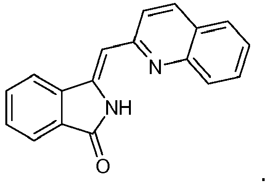

than with polymethylmethacrylate (PMMA; n = 1.8006 for 9% by weight

Figure 3 shows the corresponding fluorescence emission intensity versus wavelength spectra at an observation angle of 60° and for viewing direction vertical or horizontal to the grating lines. - A fluorescent material with higher refractive index has better waveguiding property which leads to a higher emission intensity.
- In case of


- Without being bound to theory it is believed that in this case another effect dominates over the better waveguiding effect namely the quenching of the emitter due to interactions with the matrix material. Quenching of fluorophors and phosphorescent material is a complex process and such materials interact different with different matrix polymers. On one hand the matrix can directly quench the emitter. Alternatively the interaction between both during the film formation can lead to a demixing and thus an agglomeration of the emitter. In the latter case self-quenching of the emitter can take place. Reference is made to table 1.
Table 1 Refractive Index (n) and Extinction Coefficient (k) of luminescent materials at 365 nm (ellipsometric measurements on a borofloat substrate at layer thickness 200 - 300 nm) Material Absorption maximum, nm Emission maximum, nm n k 9% of ADS066GE + 91% of PVK 374 505 1.8006 0.0280 9% of ADS066GE + 91% of PMMA 374 505 1.5201 0.0058 9% of ADS233YE + 91% of PVK 386 538 1.7546 0.0975 9% of ADS233YE + 91% of PMMA 386 538 1.5172 -0.0008 9% of ADS045YE + 91% of PVK 381 536 1.8246 0.0320 9% of ADS045YE + 91% of PMMA 381 536 1.5138 0.0100 9% of Coumarin 480 + 91% of PVK 390 452 1.8154 0.0753 9% of Counarin 480 + 91% of PMMA 390 452 1.4945 0.0103 9% of Cpd. A-1 + 91% of PVK 519 1.8829 0.1179 PMMA - - 1.4975 0.0202 PVK - - 1.5782 0.0020 - Emission intensity can be increased with amount of emitter in waveguiding layer and/or excitation power.
- The diffractive microstructure is typically provided in a low index substrate before depositing the waveguiding layer. Alternatively it is applied to the waveguiding layer, for example by embossing.
- The layer of a medium having a low index of refraction nlow can represent the substrate layer. The layer of a medium having a low index of refraction nlow may be made from PET, PC, PMMA, or acrylates. The medium having a low index of refraction nlow is preferably selected from polymethylmethacrylate, polycarbonate, polyethylenetherephatalate coated with an embossable layer, especially an embossable acrylate
- In another embodiment the layer of a medium having a low index of refraction nlow may be made of an UV-curable polymer, such as Ormocomp® made by Micro Resist Technology, or the UV curable compositions described in
WO2008/061930 (page 8 to 35). - Alternatively, the layer of a medium having a low index of refraction nlow can be a porous layer. Such porous layers are known in the art. They advantageously comprise inorganic nanoparticles, preferably in combination with one or more organic binders. Suitable inorganic nanoparticles are preferably selected from the group consisting of oxides like SiO2, Al2O3 or AlOOH.
- The substrate of the security element can be made of any suitable material known to the skilled person. The selection of the substrate depends on the intended use and the manufacturing process. Substrates may e.g. be made of glass, paper, or polymer foils. Advantageously, transparent and flexible polymer foils are used. Such foils can be selected from the group consisting of Cellulose esters (like Cellulosetriacetate, Celluloseacetate, Cellulosepropionate or Celluloseacetate/butyrate), Polyesters (like Polyethylen terephthalate PET or Polyethylen naphthalate PEN), Polyamides, Polycarbonates PC, Polymethylmetacrylates PMMA, Polyimides PI, Polyolefins, Polyvinylacetates, Polyethers, Polyvinylchloride PVC and Polyvinylsulfone PSU. Preferred are Polyesters, particularly Polyethylenterephthalate like Mylar (DuPont) or Polyethylennaphthalate, due to their exceptional stability. Suitable opaque flexible substrates are for example Polyolefin coated paper and white opaque Polyester like Melinex (DuPont).
- The refractive index of the substrate at a wavelength of about 300 to 500 nm can e.g. be in the range of 1.35 to 1.80, but typically it is between 1.49 (PMMA) and 1.59 (PC). The thickness of the substrate depends on the intended use, and on the equipment used; it is preferably between 25 µm and 200 µm. In a preferred embodiment, the substrate is "flexible"; this relates to the bending properties, in particular to enable a roll-to-roll process for manufacturing a security element.
- Optionally, the adhesion properties of the substrate may be improved by chemical or physical methods. Chemical methods include the deposition of a bonding agent, e.g. deposition of terpolymers of vinylidenchloride, acrylnitril and acrylic acid or of vinylidenchloride, methylacrylate and itaconic acid. Physical methods include plasma treatment like corona treatment. The substrates described above are commercially available or obtainable according to known methods.
- Optionally, the security element according to the invention may comprise one or more covering layers, deposited on top of the waveguiding layer. The covering layer can be made of any suitable material. To keep the waveguiding properties of the waveguiding layer with index of refraction n1, the covering layer must have at least a refractive index n4 at the absorption peak position of the luminescent material n4 < nlow - 0.005 and preferred n4 < nlow - 0.1. The selection of the material for the covering layer depends on the intended use of the security element and its manufacturing process. Suitable are e.g. the same polymers that can be used for manufacturing the low index substrate. Furthermore, the same porous materials can be used as for the layer of a medium having a low index of refraction nlow.
- Optionally, one or more additional layers are included for accommodating specific uses or needs. Such layers may e.g. be release layers or adhesive layers. Adhesive layers may be deposited as a top layer on the security element, on the side opposite to the substrate. A release layer may be a first layer on top of the substrate. Such layers, their materials and production are known in the field. Preferably, the manufacture of such layers is included in a roll-to-roll process. Depending on the security element manufactured, such additional layers need to be transparent and may require sharp interfaces.
- A method for manufacturing security elements according to the invention comprises the subsequent deposition of layers on a substrate. Accordingly, the process for manufacturing the security device, comprises the steps:
- providing a medium having a low index of refraction nlow,
- forming a diffractive microstructure in the medium having a low index of refraction nlow by embossing;
- deposition of a (polymer) layer comprising a luminescent material (waveguiding layer) on the diffractive microstructure; and optionally
- deposition of a layer of a medium having a low index of refraction nlow on the waveguiding layer; or
- providing a medium having a low index of refraction nlow,
- deposition of a (polymer) layer comprising a luminescent material (waveguiding layer) on the medium having a low index of refraction nlow;
- forming a diffractive microstructure on the waveguiding layer by embossing; and optionally
- deposition of a layer of a medium having a low index of refraction nlow on the waveguiding layer. Preferably all deposition steps are part of a roll-to-roll process.
- In a first step a layer of a medium having a low index of refraction nlow is deposited on a flexible substrate. The substrate may be transparent or opaque. Optionally, an organic binder or other additives are added to the dispersion. The layer obtained is dried, e.g. by air fans, infrared radiation or microwave radiation. The drying is done preferred in an air flow with a temperature below 60 °C. Preferably, the drying is carried out immediately after deposition.
- In a next step, a waveguiding layer comprising the luminescent material is deposited on the layer of a medium having a low index of refraction nlow. After deposition the waveguiding layer is dried if necessary.
- In a subsequent step, diffractive microstructures are embossed in the waveguiding layer, with an embossing tool, e.g. a nickel shim. The embossing may be carried out at elevated temperature and/or with UV-illumination ("hot"- and "UV"-embossing). Typically hot-embossing is done at a temperature above the glass transition temperature of the waveguiding layer. Optionally, a hardening of the polymer layer may be applied.
- In a further variant, the embossing step is done first. Thus, the diffractive microstructure is embossed, preferably hot-embossed, directly on or in the low index substrate, or in a low index embossable layer deposited on the substrate. Next, the waveguiding layer is deposited on the microstructured substrate. The same considerations regarding the indices of refraction of all layers are applicable as for the method described above. Depending i) on the viscosity of the solution or dispersion, ii) the dried layer thickness, and iii) the depth of the microstructure, the top surface of the waveguiding layer is flat, or has a diffractive microstructure correlated to the microstructure of the substrate. Optionally, on top of the waveguiding layer an additional covering layer may be deposited. One function of this layer is to protect the waveguiding layer against environmental influences and mechanical stress. Optionally, an additional polymer top coat (not shown) may be deposited, as described before. The possible materials for the substrate and the layers are the same as discussed above.
- In a further variant the coated and micro-structured foil is used to manufacture adhesive tags or labels bearing the color effect. For this purpose, the uncoated side of the substrate or the top coat of the layer stack is provided with an adhesive layer and a removable carrier protecting the adhesive layer. The latter can be e.g. silicon coated paper, or polymeric foil. The substrate with the coated layer stack is then sliced such that tags or labels of the desired size can be stripped of the carrier and applied to products, packages and the like. The known techniques of labeling tags with additional information like batch number, company logo and the like can be applied to a foil manufactured according to the invention.
- In another embodiment of both production methods, one additional release layer is deposited between the substrate and the first coated layer, and one additional adhesive layer (such as a thermo-activateable adhesive layer) is deposited as top layer. This enables a separation of the coated layer stack from the substrate and to transfer the obtained security element to another surface. With this method, it is possible to manufacture a security element that is transferable to the surface of another device such as a package, banknote, security device, e.g. by a lamination process or a hot stamping process. A security element according to this embodiment is distinctly thinner compared to a security element which is glued with an adhesive to a product or a package and the like according to the embodiment described before.
- In a particularly preferred embodiment the process for forming the security comprises the steps of;
- A) applying a curable composition (UV primer; the medium having a low index of refraction nlow) to at least a portion of the substrate;
- B) forming a diffractive microstructure on at least a portion of the curable composition;
- C) curing the composition;
- D) depositing a (polymer) layer comprising a luminescent material (waveguiding layer) on the medium having a low index of refraction nlow.
- Advantageously, the present invention involves the transfer of the diffraction gratings directly onto the surface of a substrate with high productivity and low cost.
- The forming of diffractive microstructures on the substrate comprises depositing a curable compound, or composition on at least a portion of the substrate. The composition, generally a coating or lacquer may be deposited by means of gravure, flexographic, ink jet and screen process printing. The curable lacquer may be cured by actinic radiations, preferably ultraviolet (U.V.) light or electron beam. Preferably, the lacquer is UV cured. UV curing lacquers can be obtained from BASF SE. The lacquers exposed to actinic radiations or electron beam used in the present invention are required to reach a solidified stage when they separate again from the imaging shim in order to keep the record in their upper layer of the diffraction grating image or pattern. Particularly suitable for the lacquers compositions are chemistries used in the radiation curable industries in industrial coatings and graphic arts. Particularly suitable are compositions containing one or several photo-latent catalysts that will initiate polymerization of the exposed lacquer layer to actinic radiations. Particularly suitable for fast curing and conversion to a solid state are compositions comprising one or several monomers and oligomers sensitive to free-radical polymerization, such as acrylates, methacrylates or monomers or/and oligomers, containing at least one ethylenically unsaturated group. Reference is made to
WO2008/061930 (page 8 to 35). - The curable composition is preferably curable by means of an ultraviolet (U.V.) light or an electron beam. The curable composition can be coloured.
- The (polymer) layer comprising a luminescent material (waveguiding layer) on the medium having a low index of refraction nlow is preferably made of a curable lacquer, which may be cured by actinic radiations, preferably ultraviolet (U.V.) light or electron beam. Reference is made to
WO2008/061930 (page 8 to 35). - The curable compositions are preferably deposited by means of gravure or flexographic printing.
- The diffraction grating may be formed using any methods known to the skilled man such as those described in
US4,913,858 ,US5,164,227 ,WO2005/051675 andWO2008/061930 . - Furthermore, it would be advantageous to form the diffraction gratings in register directly on the substrate.
- In said embodiment, the substrate may comprise any sheet material. The substrate may be opaque, substantially transparent or translucent, wherein the method described in
WO08/061930 - The substrate may be mould made, woven, non-woven, cast, calendared, blown, extruded and/or biaxially extruded.
- The substrate may comprise paper, fabric, man made fibres and polymeric compounds. The substrate may comprise any one or more selected from the group comprising paper, papers made from wood pulp or cotton or synthetic wood free fibres and board. The paper/board may be coated, calendared or machine glazed; coated, uncoated, mould made with cotton or denim content, Tyvac, linen, cotton, silk, leather, polythyleneterephthalate, polypropylene propafilm, polyvinylchloride, rigid PVC, cellulose, tri-acetate, acetate polystyrene, polyethylene, nylon, acrylic and polytherimide board. The polythyleneterephthalate substrate may be Melienex type film orientated polypropylene (obtainable from DuPont Films Willimington Delaware product ID Melinex HS-2).
- The substrate may comprise papers and board made from wood pulp or cotton or synthetic wood free fibres. The paper/board may be coated, calendared or machine glazed.
- The substrates being transparent filmic or non transparent substrates like opaque plastic, paper including but not limited to banknote, voucher, passport, and any other security or fiduciary documents, self adhesive stamp and excise seals, card, tobacco, pharmaceutical, computer software packaging and certificates of authentication, aluminium, and the like.
- In a preferred embodiment of the present invention the substrate is a non-transparent (opaque) sheet material, such as, for example, paper. In another preferred embodiment of the present invention the substrate is a transparent sheet material, such as, for example, polythyleneterephthalate.
- The security devices may be used in the fields of authentication, identification, and security, for a variety of purposes like (but not restricted to) banknotes, credit cards, passports, tickets, document security, anti-counterfeiting, brand protection and the like.
- For most applications, additional protective coatings are useful and are thus preferred. An additional function of the covering layer is to hamper attempts to analyze the diffractive microstructure.
- In a further embodiment, the present invention provides security elements, as described herein, which are in the form of hot or cold transferable labels, adhesive tags, and the like.
- Various features and aspects of the present invention are illustrated further in the examples that follow. While these examples are presented to show one skilled in the art how to operate within the scope of this invention, they are not to serve as a limitation on the scope of the invention where such scope is only defined in the claims. Unless otherwise indicated in the following examples and elsewhere in the specification and claims, all parts and percentages are by weight, temperatures are in degrees centigrade and pressures are at or near atmospheric.
- Rectangular gratings of 270 nm period with 140 nm depth are copied in an UV curable Ormocomp® material (commarcially available from Microresist Technology GmbH, Germany).

- The luminescent material is illuminated by collimated UV light perpendicularly to sample surface [UV LED from Nichia having an emission peak at 365 ± 5 nm; UG11 filter rejected UV light up to 400 nm; 25.6 µW/cm2 power density; measurement time: 30 s; Spectroradiometer SpectraScan PR-705 measured photoluminescence spectrum in visible region 400 - 780 nm; angle between an illumination beam and measuring direction varied from 30° to 60°].
- The emission intensity depends on the observation angle, reaching the highest level at 60°.
-
Fig. 3 is a plot of the measured emission intensity versus wavelength at a viewing angle of 60°. The emission intensity was measured for one emitting material, i.e.
- Accordingly, a logo having a "grating - no grating" structure should provide high contrast. Further a logo "grating horizontal - grating vertical" should provide a recognisable contrast and a distinct fluorescence colour change upon rotation.
Figure 4a and 4b show schematically this effect for a logo and an image, respectively. Of course the gratings do not need to be rotated by 90°, but it is expected that the contrast is maximised in this case. Gratings which are rotated by less than 90° can produce a recognisable contrast as well. The gratings should be rotated to each other by at least 20°. Preferred they are rotated by at least 30°, especially preferred by at least 45° and particularly preferred by at least 60°. -

- Emission intensity of 9 % by weight

- The highest total emission corresponds to 1000 nm thickness. Nevertheless the best contrast for the "grating horizontal - grating vertical" - or more generally two rotated gratings - case is achieved with a thickness of about 150 nm.
- A clear ultraviolet activated primer [(1-methyl-1,2-ethanediyl)bis[oxy(methyl-2,1-ethanediyl)] diacrylate (1 - 20%), poly(oxy-1,2-ethanediyl), α-hydroxy-[(1-oxo-2-propen-1-yl)oxy]-, ether with 2-ethyl-2-(hydroxymethyl)-1,3-propanediol (3:1) (10 - 50%), oligo[2-hydroxy-2-methyl-1-[4-(1-methylvinyl)phenyl]propanone] (1 - 5%), oxybis(methyl-2,1-ethanediyl) diacrylate (30 - 45%)] (91% by weight), provided by BASF, is doped with

- Encapsulation of luminescent material coated on a rectangular grating by Ormocomp® (commercially available from Microresist Technology GmbH, Germany) and Boroafloat glass shifts the emission maximum to 420 nm and 466 - 468 nm.
- Ratio of emission intensity between UV primer and

- It can provide high contrast of logo produced on a base of structure "grating - no grating".
- Rectangular gratings of 270 nm period with 140 nm depth are UV casted in clear ultraviolet activated primer [(1-methyl-1,2-ethanediyl)bis[oxy(methyl-2,1-ethanediyl)] diacrylate (1 - 20%), poly(oxy-1,2-ethanediyl), α-hydroxy-[(1-oxo-2-propen-1-yl)oxy]-, ether with 2-ethyl-2-(hydroxymethyl)-1,3-propanediol (3:1) (10 - 50%), oligo[2-hydroxy-2-methyl-1-[4-(1-methylvinyl)phenyl]propanone] (1 - 5%), oxybis(methyl-2,1-ethanediyl) diacrylate (30 - 45%)] (91% by weight) by gravure printing using a Nickel shim. Rectangular gratings are overcoated by the means of a 6 micron wireround bar coater with an ink containing 2% phtalimidine dye by weight and 1% Nitrocellulose binder in ethylacetate and methoxypropanol or with an ink containing 2 phthalimidine dye by weight and 3% vinyl chloride and vinyl acetate copolymer in methyl ethyl ketone.

- The best contrast for the "grating horizontal - grating vertical" - or more generally two rotated gratings - case is achieved with a thickness of about 150 nm.
the refractive index difference between the medium, or substrate having a low index of refraction nlow and the waveguiding layer is at least 0.1;
the microstructure period (A) is in the range of from 100 to 500 nm;
the thickness (d) of the waveguiding layer is in the range of from 60 to 200 nm; and
the microstructure depth (t) is in the range of from 100 to 300 nm,
the diffractive microstructure consists of at least two part-areas adjacent or nearby to one another, wherein one part-area comprises one groves orientation and the other part-area comprises another different groves orientation and/or one part-area comprises one grating period and the other part-area comprises another different grating period, wherein both part-areas comprise a logo in the diffractive microstructure, upon irradiation of the luminescent material the first logo appears bright and the second logo appears dark depending on the orientation of the groves and upon rotation the first logo appears dark and the second logo appears bright.
nlow and nhigh represent the refractive index at the peak of the absorption of the luminescent material. The refractive index difference between the medium, or substrate having a low index of refraction nlow and the waveguiding layer is at least 0.1.
Claims (14)
- A security device comprising:a) a layer of a medium having a low index of refraction nlow;b) a diffractive microstructure on the medium having a low index of refraction nlow;c) a waveguiding layer having a high index of refraction nhigh, which comprises a luminescent material, on the diffractive microstructure; and optionallyd) a layer of a medium having a low index of refraction nlow; orA) a layer of a medium having a low index of refraction nlow;B) a waveguiding layer having a high index of refraction nhigh; which comprises a luminescent material, on the medium having a low index of refraction nlow;C) a diffractive microstructure on the waveguiding layer having a high index of refraction nhigh; and optionallyD) a layer of a medium having a low index of refraction nlow;wherein
the refractive index difference between the medium, or substrate having a low index of refraction nlow and the waveguiding layer is at least 0.1;
the microstructure period (Λ) is in the range of from 100 to 500 nm;
the thickness (d) of the waveguiding layer is in the range of from 60 to 200 nm; and
the microstructure depth (t) is in the range of from 100 to 300 nm,
the security device being characterized in that:
the diffractive microstructure consists of at least two part-areas adjacent or nearby to one another, wherein one part-area comprises one groves orientation and the other part-area comprises another different groves orientation and/or one part-area comprises one grating period and the other part-area comprises another different grating period, wherein both part-areas comprise a logo in the diffractive microstructure, upon irradiation of the luminescent material the first logo appears bright and the second logo appears dark depending on the orientation of the groves and upon rotation the first logo appears dark and the second logo appears bright. - The security device according to claim 1, wherein the medium having a low index of refraction nlow is selected from polymethylmethacrylate, polycarbonate, and polyethylenetherephatalate coated with an embossable layer.
- The security device according to any of claims 1 or 2, wherein the waveguiding layer having a high index of refraction nhigh comprises a matrix material and the luminescent material.
- The security device according to claim 3, wherein the matrix material is selected from polyvinylcarbazole, polymethylmethacrylate, UV primer, vinyl chloride and vinyl acetate copolymers and nitrocellulose.
- The security device according to claim 4, wherein the luminescent material is selected from metal complexes, such as, for example,


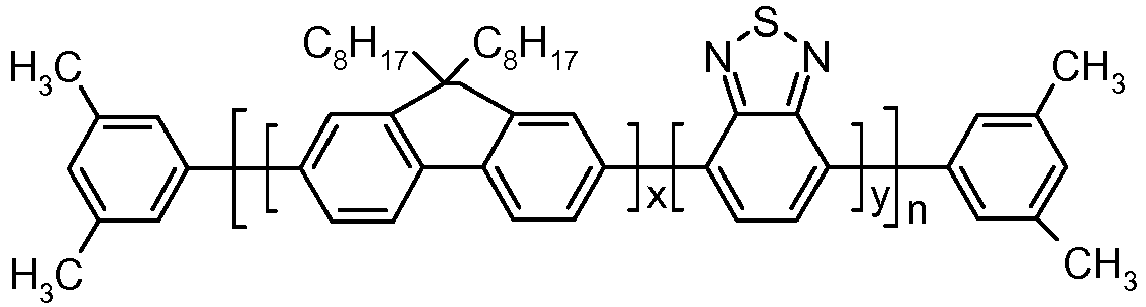

- The security device according to any of claims 1 to 5, wherein the diffractive microstructure is a diffraction grating having a microstructure period (Λ) in the range of 270 ± 30 nm; the thickness (d) of the waveguiding layer is in the range of from 140 ± 50 nm; and the microstructure depth (t) in the range of 140 ± 30 nm.
- The security device according to claim 2, wherein the embossable layer is an embossable acrylate layer.
- The security device according to claim 2, wherein the layer of a medium having a low index of refraction nlow is a porous layer.
- The security device according to claim 1, wherein the part-areas have a defined shape, such as, for example, a symbol, a stripe, a geometrical shape, a design, lettering, an alphanumeric character, the representation of an object or parts thereof.
- A process for manufacturing the security device according to claim 1, comprising the steps:- providing a medium having a low index of refraction nlow,- forming a diffractive microstructure in the medium having a low index of refraction nlow by embossing;- deposition of a polymer layer comprising a luminescent material which is the waveguiding layer having a high index of refraction nhigh on the diffractive microstructure; and optionally- deposition of a layer of a medium having a low index of refraction nlow on the waveguiding layer.
- A process for manufacturing the security device according to claim 1, comprising the steps:- providing a medium having a low index of refraction nlow,- deposition of a polymer layer comprising a luminescent material which is the waveguiding layer having a high index of refraction nhigh on the medium having a low index of refraction nlow;- forming a diffractive microstructure on the waveguiding layer by embossing; and optionally- deposition of a layer of a medium having a low index of refraction nlow on the waveguiding layer.
- The process according to claims 10, or 11, wherein all deposition steps are part of a roll-to-roll process.
- Use of the security device according to any of claims 1 to 9 in the manufacturing of banknotes, credit cards, passports, tickets and for brand protection purposes.
- A product, such as, for example, a banknote, a credit card, a passport, or a ticket, comprising the security device according to any of claims 1 to 9.
Priority Applications (1)
| Application Number | Priority Date | Filing Date | Title |
|---|---|---|---|
| EP11760796.0A EP2621730B1 (en) | 2010-09-29 | 2011-09-27 | Security element |
Applications Claiming Priority (4)
| Application Number | Priority Date | Filing Date | Title |
|---|---|---|---|
| US38749010P | 2010-09-29 | 2010-09-29 | |
| EP10182151 | 2010-09-29 | ||
| EP11760796.0A EP2621730B1 (en) | 2010-09-29 | 2011-09-27 | Security element |
| PCT/EP2011/066768 WO2012041851A1 (en) | 2010-09-29 | 2011-09-27 | Security element |
Publications (2)
| Publication Number | Publication Date |
|---|---|
| EP2621730A1 EP2621730A1 (en) | 2013-08-07 |
| EP2621730B1 true EP2621730B1 (en) | 2019-09-18 |
Family
ID=44675603
Family Applications (1)
| Application Number | Title | Priority Date | Filing Date |
|---|---|---|---|
| EP11760796.0A Active EP2621730B1 (en) | 2010-09-29 | 2011-09-27 | Security element |
Country Status (9)
| Country | Link |
|---|---|
| US (1) | US9310766B2 (en) |
| EP (1) | EP2621730B1 (en) |
| JP (1) | JP6038032B2 (en) |
| KR (1) | KR20130124494A (en) |
| CN (1) | CN103124641B (en) |
| AU (1) | AU2011310652B2 (en) |
| CA (1) | CA2811165A1 (en) |
| MX (1) | MX344784B (en) |
| WO (1) | WO2012041851A1 (en) |
Families Citing this family (34)
| Publication number | Priority date | Publication date | Assignee | Title |
|---|---|---|---|---|
| MX363517B (en) | 2011-06-21 | 2019-03-26 | Basf Se | Printing diffraction gratings on paper and board. |
| AU2012100573B4 (en) * | 2012-05-10 | 2013-03-28 | Innovia Security Pty Ltd | An optical security device |
| MX351109B (en) | 2012-09-17 | 2017-10-02 | Basf Se | Security elements and method for their manufacture. |
| GB201222813D0 (en) * | 2012-12-18 | 2013-01-30 | Rue De Int Ltd | Security device |
| US9996843B2 (en) * | 2013-12-13 | 2018-06-12 | Colorado State University Research Foundation | Nano-stamp and matched reader for anti-counterfeiting applications |
| US9515239B2 (en) | 2014-02-28 | 2016-12-06 | Panasonic Intellectual Property Management Co., Ltd. | Light-emitting device and light-emitting apparatus |
| US9618697B2 (en) * | 2014-02-28 | 2017-04-11 | Panasonic Intellectual Property Management Co., Ltd. | Light directional angle control for light-emitting device and light-emitting apparatus |
| CN105940509A (en) * | 2014-02-28 | 2016-09-14 | 松下知识产权经营株式会社 | light emitting device |
| CN105917477A (en) * | 2014-02-28 | 2016-08-31 | 松下知识产权经营株式会社 | Light-emitting element and light-emitting device |
| CN105940506A (en) * | 2014-02-28 | 2016-09-14 | 松下知识产权经营株式会社 | Light emitting device and light emitting device |
| JP2016034017A (en) * | 2014-02-28 | 2016-03-10 | パナソニックIpマネジメント株式会社 | Light emitting device |
| WO2015129222A1 (en) * | 2014-02-28 | 2015-09-03 | パナソニックIpマネジメント株式会社 | Light-emitting element and light-emitting device |
| WO2015128909A1 (en) | 2014-02-28 | 2015-09-03 | パナソニックIpマネジメント株式会社 | Light-emitting element and light-emitting device |
| US9518215B2 (en) | 2014-02-28 | 2016-12-13 | Panasonic Intellectual Property Management Co., Ltd. | Light-emitting device and light-emitting apparatus |
| JP6672585B2 (en) * | 2014-12-15 | 2020-03-25 | 凸版印刷株式会社 | Display body |
| JP6596820B2 (en) * | 2014-12-15 | 2019-10-30 | 凸版印刷株式会社 | Indicator |
| WO2016098329A1 (en) * | 2014-12-15 | 2016-06-23 | 凸版印刷株式会社 | Display, and method for manufacturing display |
| AT516688A1 (en) * | 2014-12-15 | 2016-07-15 | Hueck Folien Gmbh | Security element with color shift effect and fluorescent features, process for its preparation and its use |
| US10182702B2 (en) | 2015-03-13 | 2019-01-22 | Panasonic Intellectual Property Management Co., Ltd. | Light-emitting apparatus including photoluminescent layer |
| US10031276B2 (en) | 2015-03-13 | 2018-07-24 | Panasonic Intellectual Property Management Co., Ltd. | Display apparatus including photoluminescent layer |
| JP6566313B2 (en) * | 2015-03-13 | 2019-08-28 | パナソニックIpマネジメント株式会社 | Display device and light emitting device |
| JP6569856B2 (en) | 2015-03-13 | 2019-09-04 | パナソニックIpマネジメント株式会社 | Light emitting device and endoscope |
| JP2016171228A (en) | 2015-03-13 | 2016-09-23 | パナソニックIpマネジメント株式会社 | Light emission element, light emission device and detection device |
| JP2017005054A (en) | 2015-06-08 | 2017-01-05 | パナソニックIpマネジメント株式会社 | Light emission device |
| JP2017003697A (en) * | 2015-06-08 | 2017-01-05 | パナソニックIpマネジメント株式会社 | Light emitting element and light emitting device |
| JP2017040818A (en) | 2015-08-20 | 2017-02-23 | パナソニックIpマネジメント株式会社 | Light emitting element |
| US10359155B2 (en) | 2015-08-20 | 2019-07-23 | Panasonic Intellectual Property Management Co., Ltd. | Light-emitting apparatus |
| JP6748905B2 (en) * | 2015-08-20 | 2020-09-02 | パナソニックIpマネジメント株式会社 | Light emitting device |
| JP6719094B2 (en) | 2016-03-30 | 2020-07-08 | パナソニックIpマネジメント株式会社 | Light emitting element |
| CN116634667A (en) * | 2017-06-15 | 2023-08-22 | 捷普有限公司 | System, apparatus and method for utilizing surface mount technology on a metal substrate |
| DE102019113005A1 (en) * | 2019-05-16 | 2020-11-19 | Bundesdruckerei Gmbh | Luminescent security element |
| EP3766702A1 (en) | 2019-07-15 | 2021-01-20 | Giesecke+Devrient Currency Technology GmbH | Security element and method for manufacturing it |
| WO2022061341A1 (en) * | 2020-09-21 | 2022-03-24 | Saint-Gobain Ceramics & Plastics, Inc. | Optical light guide including fluorescent material |
| EP4506183A1 (en) * | 2023-08-08 | 2025-02-12 | Giesecke+Devrient ePayments GmbH | Method for manufacturing a card-like data carrier and card-like data carrier |
Family Cites Families (77)
| Publication number | Priority date | Publication date | Assignee | Title |
|---|---|---|---|---|
| US458475A (en) | 1891-08-25 | Rail-fastener and chair for the same | ||
| US5164227A (en) | 1987-06-19 | 1992-11-17 | Van Leer Metallized Products (Usa) Limited | Method for embossing a coated sheet with a diffraction or holographic pattern |
| US4913858A (en) | 1987-10-26 | 1990-04-03 | Dennison Manufacturing Company | Method of embossing a coated sheet with a diffraction or holographic pattern |
| DE3932505C2 (en) | 1989-09-28 | 2001-03-15 | Gao Ges Automation Org | Data carrier with an optically variable element |
| JPH07209848A (en) | 1994-01-20 | 1995-08-11 | Kimoto & Co Ltd | Light-shielding masking film |
| JPH08262963A (en) * | 1995-03-22 | 1996-10-11 | Toppan Printing Co Ltd | Image display and thermal transfer sheet used for manufacturing the same |
| JPH10129107A (en) | 1996-11-01 | 1998-05-19 | Toppan Printing Co Ltd | Image display |
| JP3845941B2 (en) * | 1997-03-25 | 2006-11-15 | 三菱化学株式会社 | Imidazole metal complex and organic electroluminescence device using the same |
| DE19731968A1 (en) * | 1997-07-24 | 1999-01-28 | Giesecke & Devrient Gmbh | Security document |
| US6451455B1 (en) | 1998-04-01 | 2002-09-17 | The Trustees Of Princeton University | Metal complexes bearing both electron transporting and hole transporting moieties |
| US6413656B1 (en) | 1998-09-14 | 2002-07-02 | The University Of Southern California | Reduced symmetry porphyrin molecules for producing enhanced luminosity from phosphorescent organic light emitting devices |
| JP3684294B2 (en) * | 1997-10-23 | 2005-08-17 | パイオニア株式会社 | Rotating body |
| JP3326390B2 (en) * | 1998-07-07 | 2002-09-24 | 日本電信電話株式会社 | Playback-only multiplex hologram card |
| US6451415B1 (en) | 1998-08-19 | 2002-09-17 | The Trustees Of Princeton University | Organic photosensitive optoelectronic device with an exciton blocking layer |
| US6830828B2 (en) | 1998-09-14 | 2004-12-14 | The Trustees Of Princeton University | Organometallic complexes as phosphorescent emitters in organic LEDs |
| US6097147A (en) | 1998-09-14 | 2000-08-01 | The Trustees Of Princeton University | Structure for high efficiency electroluminescent device |
| KR101166264B1 (en) | 1999-03-23 | 2012-07-17 | 유니버시티 오브 서던 캘리포니아 | Cyclometallated metal complexes as phosphorescent dopants in organic leds |
| KR100913568B1 (en) | 1999-05-13 | 2009-08-26 | 더 트러스티즈 오브 프린스턴 유니버시티 | Very high efficiency organic light emitting devices based on electrophosphorescence |
| US6310360B1 (en) | 1999-07-21 | 2001-10-30 | The Trustees Of Princeton University | Intersystem crossing agents for efficient utilization of excitons in organic light emitting devices |
| US6458475B1 (en) | 1999-11-24 | 2002-10-01 | The Trustee Of Princeton University | Organic light emitting diode having a blue phosphorescent molecule as an emitter |
| WO2001041512A1 (en) | 1999-12-01 | 2001-06-07 | The Trustees Of Princeton University | Complexes of form l2mx as phosphorescent dopants for organic leds |
| JP2001255808A (en) | 2000-03-09 | 2001-09-21 | Hitachi Maxell Ltd | hologram |
| JP2001265198A (en) | 2000-03-17 | 2001-09-28 | Hitachi Maxell Ltd | hologram |
| US6645645B1 (en) | 2000-05-30 | 2003-11-11 | The Trustees Of Princeton University | Phosphorescent organic light emitting devices |
| US20020121638A1 (en) | 2000-06-30 | 2002-09-05 | Vladimir Grushin | Electroluminescent iridium compounds with fluorinated phenylpyridines, phenylpyrimidines, and phenylquinolines and devices made with such compounds |
| CN101924190B (en) | 2000-08-11 | 2012-07-04 | 普林斯顿大学理事会 | Organometallic compounds and emission-shifting organic electrophosphorescence |
| JP2002072835A (en) | 2000-08-31 | 2002-03-12 | Dainippon Printing Co Ltd | Information recording medium having optical diffraction structure accompanied by invisible information, label for producing the information recording medium, and transfer sheet for producing the information recording medium |
| JP4086498B2 (en) | 2000-11-29 | 2008-05-14 | キヤノン株式会社 | Metal coordination compound, light emitting device and display device |
| KR100865096B1 (en) | 2000-11-30 | 2008-10-24 | 캐논 가부시끼가이샤 | Light emitting element and display device |
| AU2002222565A1 (en) | 2000-11-30 | 2002-06-11 | Canon Kabushiki Kaisha | Luminescent element and display |
| JP4154145B2 (en) | 2000-12-01 | 2008-09-24 | キヤノン株式会社 | Metal coordination compound, light emitting device and display device |
| US6573651B2 (en) | 2000-12-18 | 2003-06-03 | The Trustees Of Princeton University | Highly efficient OLEDs using doped ambipolar conductive molecular organic thin films |
| WO2002071813A1 (en) | 2001-03-02 | 2002-09-12 | The Trustees Of Princeton University | Double doped-layer, phosphorescent organic light emitting devices |
| JP4307000B2 (en) | 2001-03-08 | 2009-08-05 | キヤノン株式会社 | Metal coordination compound, electroluminescent element and display device |
| JP4438042B2 (en) | 2001-03-08 | 2010-03-24 | キヤノン株式会社 | Metal coordination compound, electroluminescent element and display device |
| JP4307001B2 (en) | 2001-03-14 | 2009-08-05 | キヤノン株式会社 | Metal coordination compound, electroluminescent element and display device |
| AU2002306698A1 (en) | 2001-03-14 | 2002-09-24 | The Trustees Of Princeton University | Materials and devices for blue phosphorescence based organic light emitting diodes |
| JP2002286941A (en) * | 2001-03-28 | 2002-10-03 | Harison Toshiba Lighting Corp | Light guide and planar light emitting device |
| KR100888424B1 (en) | 2001-05-16 | 2009-03-11 | 더 트러스티즈 오브 프린스턴 유니버시티 | High efficiency multicolor electro organic light emitting device |
| JP3650082B2 (en) | 2001-06-04 | 2005-05-18 | 三洋電機株式会社 | Organic electroluminescence device, light emitting material, and organic compound |
| WO2002104080A1 (en) | 2001-06-15 | 2002-12-27 | Canon Kabushiki Kaisha | Organic electroluminescnece device |
| US7067202B2 (en) | 2001-06-15 | 2006-06-27 | Sanyo Electric Co., Ltd. | Luminescent organometallic compound and light emitting device |
| JP4310077B2 (en) | 2001-06-19 | 2009-08-05 | キヤノン株式会社 | Metal coordination compound and organic light emitting device |
| EP1421827B1 (en) | 2001-08-29 | 2012-02-22 | The Trustees Of Princeton University | Organic light emitting devices having carrier blocking layers comprising metal complexes |
| JP3960765B2 (en) | 2001-09-03 | 2007-08-15 | 三洋電機株式会社 | Luminescent material for light emitting device |
| JP2003073387A (en) | 2001-09-04 | 2003-03-12 | Canon Inc | Metal coordination compound and organic light emitting device |
| DE10150293B4 (en) | 2001-10-12 | 2005-05-12 | Ovd Kinegram Ag | security element |
| US6835469B2 (en) | 2001-10-17 | 2004-12-28 | The University Of Southern California | Phosphorescent compounds and devices comprising the same |
| US6869695B2 (en) | 2001-12-28 | 2005-03-22 | The Trustees Of Princeton University | White light emitting OLEDs from combined monomer and aggregate emission |
| JP2003248414A (en) | 2002-02-22 | 2003-09-05 | Ntt Advanced Technology Corp | Waveguide hologram type forgery prevention seal |
| US7491472B2 (en) * | 2002-07-26 | 2009-02-17 | Dai Nippon Printing Co., Ltd. | Volume hologram transfer foil |
| JP2004223975A (en) * | 2003-01-27 | 2004-08-12 | Toppan Printing Co Ltd | Forgery prevention medium, information display medium, forgery prevention transfer foil, forgery prevention seal, and methods for manufacturing them |
| DE10338550A1 (en) | 2003-08-19 | 2005-03-31 | Basf Ag | Transition metal complexes with carbene ligands as emitters for organic light-emitting diodes (OLEDs) |
| GB0326576D0 (en) | 2003-11-14 | 2003-12-17 | Printetch Ltd | Printing composition |
| WO2005113704A2 (en) | 2004-05-18 | 2005-12-01 | The University Of Southern California | Luminescent compounds with carbene ligands |
| WO2006000544A2 (en) | 2004-06-28 | 2006-01-05 | Ciba Specialty Chemicals Holding Inc. | Electroluminescent metal complexes with triazoles and benzotriazoles |
| GB0417422D0 (en) | 2004-08-05 | 2004-09-08 | Suisse Electronique Microtech | Security device |
| DE102005011612A1 (en) * | 2004-08-13 | 2006-02-23 | Giesecke & Devrient Gmbh | Data carrier with an optically variable structure |
| DE102004049118A1 (en) * | 2004-10-07 | 2006-04-13 | Giesecke & Devrient Gmbh | Security element and method for its production |
| DE102004057072A1 (en) | 2004-11-25 | 2006-06-01 | Basf Ag | Use of Transition Metal Carbene Complexes in Organic Light Emitting Diodes (OLEDs) |
| DE102005017169B4 (en) * | 2005-04-13 | 2023-06-22 | Ovd Kinegram Ag | transfer film |
| DE102005039320A1 (en) * | 2005-08-19 | 2007-02-22 | Giesecke & Devrient Gmbh | Card-shaped data carrier |
| JP2007072188A (en) * | 2005-09-07 | 2007-03-22 | Dainippon Printing Co Ltd | Hologram, hologram label and hologram transfer foil |
| CN103880891A (en) | 2006-04-04 | 2014-06-25 | 巴斯夫欧洲公司 | Transition metal complexes comprising one noncarbene ligand and one or two carbene ligands and their use in oleds |
| ATE550342T1 (en) | 2006-04-05 | 2012-04-15 | Basf Se | HETEROLEPTIC TRANSITION METAL-CARBEN COMPLEXES AND THEIR USE IN ORGANIC LIGHT-LIGHT DIODES (OLEDS) |
| EP1862827B2 (en) | 2006-05-31 | 2012-05-30 | CSEM Centre Suisse d'Electronique et de Microtechnique SA - Recherche et Développement | Nano-structured Zero-order diffractive filter |
| JP2009541431A (en) | 2006-06-26 | 2009-11-26 | ビーエーエスエフ ソシエタス・ヨーロピア | Use of transition metal-carbene complexes without cyclometalation via non-carbene |
| BRPI0719110A2 (en) | 2006-11-21 | 2013-12-10 | Ciba Holding Inc | APPARATUS AND METHOD FOR MANUFACTURING A SAFETY PRODUCT |
| WO2008101842A1 (en) | 2007-02-23 | 2008-08-28 | Basf Se | Electroluminescent metal complexes with benzotriazoles |
| DE102007024298B3 (en) * | 2007-05-23 | 2008-10-16 | Zahedi Fariborz Martin Loessl | Film element for authentication, security paper, security document, security document, coin, token, commodity, design element and method for producing a film element for authentication and method for producing a security paper, a security document and a value document such as a banknote |
| JP5292769B2 (en) | 2007-11-06 | 2013-09-18 | 大日本印刷株式会社 | Organic electroluminescence device |
| WO2009077350A1 (en) | 2007-12-14 | 2009-06-25 | Basf Se | Inorganic phosphor, obtainable by wet milling |
| DE102008013167A1 (en) * | 2008-03-07 | 2009-09-10 | Giesecke & Devrient Gmbh | Security element and method for its production |
| EP2130884A1 (en) | 2008-06-02 | 2009-12-09 | Hueck Folien Ges.m.b.H. | Safety sticker or adhesive band |
| JP5705129B2 (en) | 2008-12-19 | 2015-04-22 | ビーエーエスエフ ソシエタス・ヨーロピアBasf Se | Thin aluminum flakes |
| AU2010285107A1 (en) | 2009-08-21 | 2012-03-15 | Basf Se | Apparatus and method for a sub microscopic and optically variable image carrying device |
| JP6164845B2 (en) | 2009-11-27 | 2017-07-19 | ビーエーエスエフ ソシエタス・ヨーロピアBasf Se | Coating composition for security elements and holograms |
-
2011
- 2011-09-27 AU AU2011310652A patent/AU2011310652B2/en not_active Ceased
- 2011-09-27 JP JP2013530702A patent/JP6038032B2/en not_active Expired - Fee Related
- 2011-09-27 CN CN201180046969.7A patent/CN103124641B/en not_active Expired - Fee Related
- 2011-09-27 EP EP11760796.0A patent/EP2621730B1/en active Active
- 2011-09-27 MX MX2013003583A patent/MX344784B/en active IP Right Grant
- 2011-09-27 CA CA2811165A patent/CA2811165A1/en not_active Abandoned
- 2011-09-27 US US13/823,348 patent/US9310766B2/en not_active Expired - Fee Related
- 2011-09-27 WO PCT/EP2011/066768 patent/WO2012041851A1/en not_active Ceased
- 2011-09-27 KR KR1020137010520A patent/KR20130124494A/en not_active Withdrawn
Non-Patent Citations (1)
| Title |
|---|
| None * |
Also Published As
| Publication number | Publication date |
|---|---|
| JP6038032B2 (en) | 2016-12-07 |
| CN103124641B (en) | 2015-12-09 |
| US9310766B2 (en) | 2016-04-12 |
| AU2011310652A1 (en) | 2013-04-18 |
| WO2012041851A1 (en) | 2012-04-05 |
| US20130208327A1 (en) | 2013-08-15 |
| AU2011310652B2 (en) | 2014-10-16 |
| KR20130124494A (en) | 2013-11-14 |
| JP2013546007A (en) | 2013-12-26 |
| MX2013003583A (en) | 2013-05-31 |
| EP2621730A1 (en) | 2013-08-07 |
| CA2811165A1 (en) | 2012-04-05 |
| CN103124641A (en) | 2013-05-29 |
| MX344784B (en) | 2017-01-06 |
Similar Documents
| Publication | Publication Date | Title |
|---|---|---|
| US9310766B2 (en) | Security element | |
| CN102574411B (en) | Method for producing multilayer body and multilayer body | |
| US10926571B2 (en) | Method for producing a multilayer element, and multilayer element | |
| RU2267406C2 (en) | Method of producing data carrier printed by means of laser, data carrier produced by the method and blank for the carrier | |
| CN102656021B (en) | Security document with security feature on edge | |
| EP3459756B1 (en) | Counterfeit-preventing structure | |
| KR102746922B1 (en) | Uses of 4-bora-3A,4A-diaza-S-indacene for security purposes | |
| TW201841781A (en) | Method for producing a multilayer film and multilayer film as well as a security element and a security document | |
| JP2003520986A (en) | Optical modulation security device | |
| JP2016533921A5 (en) | ||
| AU2008253372A2 (en) | Film element for detecting authenticity | |
| JP4498825B2 (en) | Hologram transfer sheet and printed matter | |
| FR3007318A1 (en) | MULTILAYER SAFETY STRUCTURE AND METHOD OF MANUFACTURING THE SAME | |
| KR100506131B1 (en) | Hologram ribbon and its manufacturing method which has anti-counterfeiting function | |
| JP6686346B2 (en) | Hologram laminate, information recording medium, and method for manufacturing hologram laminate | |
| JP2007106005A (en) | Laminate film and its usage | |
| JP6686347B2 (en) | Hologram laminate, information recording medium, and method for manufacturing hologram laminate | |
| EP3154787B2 (en) | Method of manufacturing a multilayer data carrier having security inscriptions | |
| HK1169082A (en) | Transfer foil comprising optically variable magnetic pigment, method of making, use of transfer foil, and article or document comprising such |
Legal Events
| Date | Code | Title | Description |
|---|---|---|---|
| PUAI | Public reference made under article 153(3) epc to a published international application that has entered the european phase |
Free format text: ORIGINAL CODE: 0009012 |
|
| 17P | Request for examination filed |
Effective date: 20130429 |
|
| AK | Designated contracting states |
Kind code of ref document: A1 Designated state(s): AL AT BE BG CH CY CZ DE DK EE ES FI FR GB GR HR HU IE IS IT LI LT LU LV MC MK MT NL NO PL PT RO RS SE SI SK SM TR |
|
| DAX | Request for extension of the european patent (deleted) | ||
| STAA | Information on the status of an ep patent application or granted ep patent |
Free format text: STATUS: EXAMINATION IS IN PROGRESS |
|
| 17Q | First examination report despatched |
Effective date: 20170123 |
|
| REG | Reference to a national code |
Ref country code: DE Ref legal event code: R079 Ref document number: 602011062163 Country of ref document: DE Free format text: PREVIOUS MAIN CLASS: B41M0003140000 Ipc: G03H0001000000 |
|
| RIC1 | Information provided on ipc code assigned before grant |
Ipc: B41M 3/14 20060101ALI20190311BHEP Ipc: B42D 25/29 20140101ALI20190311BHEP Ipc: G03H 1/02 20060101ALI20190311BHEP Ipc: B42D 25/387 20140101ALI20190311BHEP Ipc: G03H 1/00 20060101AFI20190311BHEP Ipc: B42D 25/373 20140101ALI20190311BHEP |
|
| GRAP | Despatch of communication of intention to grant a patent |
Free format text: ORIGINAL CODE: EPIDOSNIGR1 |
|
| STAA | Information on the status of an ep patent application or granted ep patent |
Free format text: STATUS: GRANT OF PATENT IS INTENDED |
|
| INTG | Intention to grant announced |
Effective date: 20190506 |
|
| GRAS | Grant fee paid |
Free format text: ORIGINAL CODE: EPIDOSNIGR3 |
|
| GRAA | (expected) grant |
Free format text: ORIGINAL CODE: 0009210 |
|
| STAA | Information on the status of an ep patent application or granted ep patent |
Free format text: STATUS: THE PATENT HAS BEEN GRANTED |
|
| AK | Designated contracting states |
Kind code of ref document: B1 Designated state(s): AL AT BE BG CH CY CZ DE DK EE ES FI FR GB GR HR HU IE IS IT LI LT LU LV MC MK MT NL NO PL PT RO RS SE SI SK SM TR |
|
| REG | Reference to a national code |
Ref country code: GB Ref legal event code: FG4D |
|
| REG | Reference to a national code |
Ref country code: CH Ref legal event code: EP |
|
| REG | Reference to a national code |
Ref country code: DE Ref legal event code: R096 Ref document number: 602011062163 Country of ref document: DE |
|
| REG | Reference to a national code |
Ref country code: AT Ref legal event code: REF Ref document number: 1182048 Country of ref document: AT Kind code of ref document: T Effective date: 20191015 |
|
| REG | Reference to a national code |
Ref country code: IE Ref legal event code: FG4D |
|
| REG | Reference to a national code |
Ref country code: NL Ref legal event code: MP Effective date: 20190918 |
|
| PG25 | Lapsed in a contracting state [announced via postgrant information from national office to epo] |
Ref country code: LT Free format text: LAPSE BECAUSE OF FAILURE TO SUBMIT A TRANSLATION OF THE DESCRIPTION OR TO PAY THE FEE WITHIN THE PRESCRIBED TIME-LIMIT Effective date: 20190918 Ref country code: FI Free format text: LAPSE BECAUSE OF FAILURE TO SUBMIT A TRANSLATION OF THE DESCRIPTION OR TO PAY THE FEE WITHIN THE PRESCRIBED TIME-LIMIT Effective date: 20190918 Ref country code: BG Free format text: LAPSE BECAUSE OF FAILURE TO SUBMIT A TRANSLATION OF THE DESCRIPTION OR TO PAY THE FEE WITHIN THE PRESCRIBED TIME-LIMIT Effective date: 20191218 Ref country code: NO Free format text: LAPSE BECAUSE OF FAILURE TO SUBMIT A TRANSLATION OF THE DESCRIPTION OR TO PAY THE FEE WITHIN THE PRESCRIBED TIME-LIMIT Effective date: 20191218 Ref country code: SE Free format text: LAPSE BECAUSE OF FAILURE TO SUBMIT A TRANSLATION OF THE DESCRIPTION OR TO PAY THE FEE WITHIN THE PRESCRIBED TIME-LIMIT Effective date: 20190918 Ref country code: HR Free format text: LAPSE BECAUSE OF FAILURE TO SUBMIT A TRANSLATION OF THE DESCRIPTION OR TO PAY THE FEE WITHIN THE PRESCRIBED TIME-LIMIT Effective date: 20190918 |
|
| REG | Reference to a national code |
Ref country code: LT Ref legal event code: MG4D |
|
| PG25 | Lapsed in a contracting state [announced via postgrant information from national office to epo] |
Ref country code: GR Free format text: LAPSE BECAUSE OF FAILURE TO SUBMIT A TRANSLATION OF THE DESCRIPTION OR TO PAY THE FEE WITHIN THE PRESCRIBED TIME-LIMIT Effective date: 20191219 Ref country code: LV Free format text: LAPSE BECAUSE OF FAILURE TO SUBMIT A TRANSLATION OF THE DESCRIPTION OR TO PAY THE FEE WITHIN THE PRESCRIBED TIME-LIMIT Effective date: 20190918 Ref country code: AL Free format text: LAPSE BECAUSE OF FAILURE TO SUBMIT A TRANSLATION OF THE DESCRIPTION OR TO PAY THE FEE WITHIN THE PRESCRIBED TIME-LIMIT Effective date: 20190918 Ref country code: RS Free format text: LAPSE BECAUSE OF FAILURE TO SUBMIT A TRANSLATION OF THE DESCRIPTION OR TO PAY THE FEE WITHIN THE PRESCRIBED TIME-LIMIT Effective date: 20190918 |
|
| REG | Reference to a national code |
Ref country code: AT Ref legal event code: MK05 Ref document number: 1182048 Country of ref document: AT Kind code of ref document: T Effective date: 20190918 |
|
| PG25 | Lapsed in a contracting state [announced via postgrant information from national office to epo] |
Ref country code: NL Free format text: LAPSE BECAUSE OF FAILURE TO SUBMIT A TRANSLATION OF THE DESCRIPTION OR TO PAY THE FEE WITHIN THE PRESCRIBED TIME-LIMIT Effective date: 20190918 Ref country code: PT Free format text: LAPSE BECAUSE OF FAILURE TO SUBMIT A TRANSLATION OF THE DESCRIPTION OR TO PAY THE FEE WITHIN THE PRESCRIBED TIME-LIMIT Effective date: 20200120 Ref country code: AT Free format text: LAPSE BECAUSE OF FAILURE TO SUBMIT A TRANSLATION OF THE DESCRIPTION OR TO PAY THE FEE WITHIN THE PRESCRIBED TIME-LIMIT Effective date: 20190918 Ref country code: EE Free format text: LAPSE BECAUSE OF FAILURE TO SUBMIT A TRANSLATION OF THE DESCRIPTION OR TO PAY THE FEE WITHIN THE PRESCRIBED TIME-LIMIT Effective date: 20190918 Ref country code: PL Free format text: LAPSE BECAUSE OF FAILURE TO SUBMIT A TRANSLATION OF THE DESCRIPTION OR TO PAY THE FEE WITHIN THE PRESCRIBED TIME-LIMIT Effective date: 20190918 Ref country code: IT Free format text: LAPSE BECAUSE OF FAILURE TO SUBMIT A TRANSLATION OF THE DESCRIPTION OR TO PAY THE FEE WITHIN THE PRESCRIBED TIME-LIMIT Effective date: 20190918 Ref country code: ES Free format text: LAPSE BECAUSE OF FAILURE TO SUBMIT A TRANSLATION OF THE DESCRIPTION OR TO PAY THE FEE WITHIN THE PRESCRIBED TIME-LIMIT Effective date: 20190918 Ref country code: RO Free format text: LAPSE BECAUSE OF FAILURE TO SUBMIT A TRANSLATION OF THE DESCRIPTION OR TO PAY THE FEE WITHIN THE PRESCRIBED TIME-LIMIT Effective date: 20190918 |
|
| PG25 | Lapsed in a contracting state [announced via postgrant information from national office to epo] |
Ref country code: SM Free format text: LAPSE BECAUSE OF FAILURE TO SUBMIT A TRANSLATION OF THE DESCRIPTION OR TO PAY THE FEE WITHIN THE PRESCRIBED TIME-LIMIT Effective date: 20190918 Ref country code: CZ Free format text: LAPSE BECAUSE OF FAILURE TO SUBMIT A TRANSLATION OF THE DESCRIPTION OR TO PAY THE FEE WITHIN THE PRESCRIBED TIME-LIMIT Effective date: 20190918 Ref country code: SK Free format text: LAPSE BECAUSE OF FAILURE TO SUBMIT A TRANSLATION OF THE DESCRIPTION OR TO PAY THE FEE WITHIN THE PRESCRIBED TIME-LIMIT Effective date: 20190918 Ref country code: IS Free format text: LAPSE BECAUSE OF FAILURE TO SUBMIT A TRANSLATION OF THE DESCRIPTION OR TO PAY THE FEE WITHIN THE PRESCRIBED TIME-LIMIT Effective date: 20200224 |
|
| REG | Reference to a national code |
Ref country code: DE Ref legal event code: R097 Ref document number: 602011062163 Country of ref document: DE |
|
| PLBE | No opposition filed within time limit |
Free format text: ORIGINAL CODE: 0009261 |
|
| STAA | Information on the status of an ep patent application or granted ep patent |
Free format text: STATUS: NO OPPOSITION FILED WITHIN TIME LIMIT |
|
| PG2D | Information on lapse in contracting state deleted |
Ref country code: IS |
|
| PG25 | Lapsed in a contracting state [announced via postgrant information from national office to epo] |
Ref country code: LU Free format text: LAPSE BECAUSE OF NON-PAYMENT OF DUE FEES Effective date: 20190927 Ref country code: IE Free format text: LAPSE BECAUSE OF NON-PAYMENT OF DUE FEES Effective date: 20190927 Ref country code: DK Free format text: LAPSE BECAUSE OF FAILURE TO SUBMIT A TRANSLATION OF THE DESCRIPTION OR TO PAY THE FEE WITHIN THE PRESCRIBED TIME-LIMIT Effective date: 20190918 Ref country code: IS Free format text: LAPSE BECAUSE OF FAILURE TO SUBMIT A TRANSLATION OF THE DESCRIPTION OR TO PAY THE FEE WITHIN THE PRESCRIBED TIME-LIMIT Effective date: 20200119 |
|
| REG | Reference to a national code |
Ref country code: BE Ref legal event code: MM Effective date: 20190930 |
|
| 26N | No opposition filed |
Effective date: 20200619 |
|
| PG25 | Lapsed in a contracting state [announced via postgrant information from national office to epo] |
Ref country code: SI Free format text: LAPSE BECAUSE OF FAILURE TO SUBMIT A TRANSLATION OF THE DESCRIPTION OR TO PAY THE FEE WITHIN THE PRESCRIBED TIME-LIMIT Effective date: 20190918 Ref country code: BE Free format text: LAPSE BECAUSE OF NON-PAYMENT OF DUE FEES Effective date: 20190930 Ref country code: MC Free format text: LAPSE BECAUSE OF FAILURE TO SUBMIT A TRANSLATION OF THE DESCRIPTION OR TO PAY THE FEE WITHIN THE PRESCRIBED TIME-LIMIT Effective date: 20190918 |
|
| PG25 | Lapsed in a contracting state [announced via postgrant information from national office to epo] |
Ref country code: FR Free format text: LAPSE BECAUSE OF NON-PAYMENT OF DUE FEES Effective date: 20191118 |
|
| PG25 | Lapsed in a contracting state [announced via postgrant information from national office to epo] |
Ref country code: CY Free format text: LAPSE BECAUSE OF FAILURE TO SUBMIT A TRANSLATION OF THE DESCRIPTION OR TO PAY THE FEE WITHIN THE PRESCRIBED TIME-LIMIT Effective date: 20190918 |
|
| PG25 | Lapsed in a contracting state [announced via postgrant information from national office to epo] |
Ref country code: HU Free format text: LAPSE BECAUSE OF FAILURE TO SUBMIT A TRANSLATION OF THE DESCRIPTION OR TO PAY THE FEE WITHIN THE PRESCRIBED TIME-LIMIT; INVALID AB INITIO Effective date: 20110927 Ref country code: MT Free format text: LAPSE BECAUSE OF FAILURE TO SUBMIT A TRANSLATION OF THE DESCRIPTION OR TO PAY THE FEE WITHIN THE PRESCRIBED TIME-LIMIT Effective date: 20190918 |
|
| PG25 | Lapsed in a contracting state [announced via postgrant information from national office to epo] |
Ref country code: TR Free format text: LAPSE BECAUSE OF FAILURE TO SUBMIT A TRANSLATION OF THE DESCRIPTION OR TO PAY THE FEE WITHIN THE PRESCRIBED TIME-LIMIT Effective date: 20190918 |
|
| PG25 | Lapsed in a contracting state [announced via postgrant information from national office to epo] |
Ref country code: MK Free format text: LAPSE BECAUSE OF FAILURE TO SUBMIT A TRANSLATION OF THE DESCRIPTION OR TO PAY THE FEE WITHIN THE PRESCRIBED TIME-LIMIT Effective date: 20190918 |
|
| PGFP | Annual fee paid to national office [announced via postgrant information from national office to epo] |
Ref country code: GB Payment date: 20220920 Year of fee payment: 12 Ref country code: DE Payment date: 20220527 Year of fee payment: 12 |
|
| PGFP | Annual fee paid to national office [announced via postgrant information from national office to epo] |
Ref country code: CH Payment date: 20220928 Year of fee payment: 12 |
|
| REG | Reference to a national code |
Ref country code: DE Ref legal event code: R119 Ref document number: 602011062163 Country of ref document: DE |
|
| REG | Reference to a national code |
Ref country code: CH Ref legal event code: PL |
|
| GBPC | Gb: european patent ceased through non-payment of renewal fee |
Effective date: 20230927 |
|
| PG25 | Lapsed in a contracting state [announced via postgrant information from national office to epo] |
Ref country code: GB Free format text: LAPSE BECAUSE OF NON-PAYMENT OF DUE FEES Effective date: 20230927 |
|
| PG25 | Lapsed in a contracting state [announced via postgrant information from national office to epo] |
Ref country code: CH Free format text: LAPSE BECAUSE OF NON-PAYMENT OF DUE FEES Effective date: 20230930 |
|
| PG25 | Lapsed in a contracting state [announced via postgrant information from national office to epo] |
Ref country code: GB Free format text: LAPSE BECAUSE OF NON-PAYMENT OF DUE FEES Effective date: 20230927 Ref country code: DE Free format text: LAPSE BECAUSE OF NON-PAYMENT OF DUE FEES Effective date: 20240403 Ref country code: CH Free format text: LAPSE BECAUSE OF NON-PAYMENT OF DUE FEES Effective date: 20230930 |