EP2618423B1 - Antenna device for portable terminal - Google Patents
Antenna device for portable terminal Download PDFInfo
- Publication number
- EP2618423B1 EP2618423B1 EP12199259.8A EP12199259A EP2618423B1 EP 2618423 B1 EP2618423 B1 EP 2618423B1 EP 12199259 A EP12199259 A EP 12199259A EP 2618423 B1 EP2618423 B1 EP 2618423B1
- Authority
- EP
- European Patent Office
- Prior art keywords
- slot
- antenna element
- antenna
- portable terminal
- pcb
- Prior art date
- Legal status (The legal status is an assumption and is not a legal conclusion. Google has not performed a legal analysis and makes no representation as to the accuracy of the status listed.)
- Not-in-force
Links
Images


Classifications
-
- H—ELECTRICITY
- H01—ELECTRIC ELEMENTS
- H01Q—ANTENNAS, i.e. RADIO AERIALS
- H01Q1/00—Details of, or arrangements associated with, antennas
- H01Q1/12—Supports; Mounting means
- H01Q1/22—Supports; Mounting means by structural association with other equipment or articles
- H01Q1/24—Supports; Mounting means by structural association with other equipment or articles with receiving set
- H01Q1/241—Supports; Mounting means by structural association with other equipment or articles with receiving set used in mobile communications, e.g. GSM
- H01Q1/242—Supports; Mounting means by structural association with other equipment or articles with receiving set used in mobile communications, e.g. GSM specially adapted for hand-held use
- H01Q1/243—Supports; Mounting means by structural association with other equipment or articles with receiving set used in mobile communications, e.g. GSM specially adapted for hand-held use with built-in antennas
-
- H—ELECTRICITY
- H01—ELECTRIC ELEMENTS
- H01Q—ANTENNAS, i.e. RADIO AERIALS
- H01Q1/00—Details of, or arrangements associated with, antennas
- H01Q1/12—Supports; Mounting means
- H01Q1/22—Supports; Mounting means by structural association with other equipment or articles
- H01Q1/24—Supports; Mounting means by structural association with other equipment or articles with receiving set
-
- H—ELECTRICITY
- H01—ELECTRIC ELEMENTS
- H01Q—ANTENNAS, i.e. RADIO AERIALS
- H01Q1/00—Details of, or arrangements associated with, antennas
- H01Q1/44—Details of, or arrangements associated with, antennas using equipment having another main function to serve additionally as an antenna, e.g. means for giving an antenna an aesthetic aspect
- H01Q1/46—Electric supply lines or communication lines
-
- H—ELECTRICITY
- H01—ELECTRIC ELEMENTS
- H01Q—ANTENNAS, i.e. RADIO AERIALS
- H01Q1/00—Details of, or arrangements associated with, antennas
- H01Q1/52—Means for reducing coupling between antennas; Means for reducing coupling between an antenna and another structure
-
- H—ELECTRICITY
- H01—ELECTRIC ELEMENTS
- H01Q—ANTENNAS, i.e. RADIO AERIALS
- H01Q13/00—Waveguide horns or mouths; Slot antennas; Leaky-waveguide antennas; Equivalent structures causing radiation along the transmission path of a guided wave
- H01Q13/10—Resonant slot antennas
-
- H—ELECTRICITY
- H01—ELECTRIC ELEMENTS
- H01Q—ANTENNAS, i.e. RADIO AERIALS
- H01Q5/00—Arrangements for simultaneous operation of antennas on two or more different wavebands, e.g. dual-band or multi-band arrangements
- H01Q5/30—Arrangements for providing operation on different wavebands
- H01Q5/378—Combination of fed elements with parasitic elements
- H01Q5/385—Two or more parasitic elements
-
- H—ELECTRICITY
- H01—ELECTRIC ELEMENTS
- H01Q—ANTENNAS, i.e. RADIO AERIALS
- H01Q9/00—Electrically-short antennas having dimensions not more than twice the operating wavelength and consisting of conductive active radiating elements
- H01Q9/04—Resonant antennas
- H01Q9/30—Resonant antennas with feed to end of elongated active element, e.g. unipole
- H01Q9/42—Resonant antennas with feed to end of elongated active element, e.g. unipole with folded element, the folded parts being spaced apart a small fraction of the operating wavelength
Definitions
- the present disclosure relates generally to antennas, and more particularly, to a portable terminal comprising an antenna device.
- Portable (i.e., hand held) terminals such as mobile communication terminals (cellular phones), electronic schedulers, and personal complex terminals have become necessities of current society based on the recent technological advances in the telecommunications industry.
- the portable terminals have been developed into important means of information transmission, which are quickly changed.
- the portable terminal has an antenna for wireless communication.
- the antenna is embedded in the portable terminal to beautify and miniaturize the portable terminal. It is preferable that the embedded antenna meets required performance metrics to smoothly transmit and receive signals in a corresponding communication service band.
- WO 03/088414 discloses a broad band antenna provided with a radiator, for example a slot in an earth plane.
- a supply means has a first central conductor which, with one end, is connected to the circuits in a transceiver which extends along/in association with the radiator and which has one free end.
- the supply means further has a second, helical conductor whose one end is earthed and whose other end terminates freely.
- the helical conductor surrounds the central conductor.
- the helical conductor is provided with straight, mutually intersecting conductor sections on opposing sides of a three-layer circuit card. The opposing ends of the conductor sections are electrically connected to one another through the circuit card, and the central conductor is disposed in the central layer of the card.
- AMJAD A OMAR ET AL "Design and Measurement of Self-Matched Dual-Frequency Coplanar Waveguide-Fed-Slot Antennas", IEEE TRANSACTIONS ON ANTENNAS AND PROPAGATION, IEEE SERVICE CENTER, PISCATAWAY, NJ, US, vol. 55, no. 1, 1 January 2007 (2007-01-01), pages 223-226 , discloses two designs of dual frequency co-planar waveguide (CPW)-fed double folded slot antennas wherein the CPW is used to feed two double folded slot antennas of different bands resulting in dual band operation.
- CPW co-planar waveguide
- a handheld electronic device may have a housing in which electrical components such as integrated circuits and a broadband antenna are mounted.
- the broadband antenna may have a ground element and a resonating element.
- the resonating element may have two arms of unequal length and may have a self-resonant element.
- the antenna may have a feed terminal connected to the self-resonant element and a ground terminal connected to the ground element.
- the self-resonant element may be near-field coupled to one of the arms of the resonating element.
- the self-resonant element may be formed using a conductive rectangular element that is not electrically shorted to the ground element or the arms of the resonating element.
- the antenna may operate over first and second frequency ranges of interest.
- An aspect of the present invention is to solve at least the above-mentioned problems and/or disadvantages and to provide at least the advantages described below. Accordingly, present invention relates to a portable terminal comprising an antenna device according to claim 1.
- the antenna device is inter alia comprised of first and second antenna elements.
- the first antenna element includes at least a portion of one or more metal members disposed within the portable terminal; is electrically connected with a ground surface of the PCB; and has a slot.
- the second antenna element is disposed in proximity to the slot, spaced from and electromagnetically coupled to the first antenna element.
- the second antenna element receives RF power from the PCB and is configured to resonate at a frequency of the RF power.
- the present invention relates to an antenna device for securing antenna performance using one or more metal members installed in a portable terminal.
- Embodiments described hereinafter relate to an antenna device capable of securing antenna performance using one or more metal members installed for a corresponding purpose (e.g., for decoration) in a portable terminal.
- Embodiments enable a metal member installed in a portable terminal to enhance antenna performance rather than degrading antenna performance as in prior art designs.
- An antenna device according to one embodiment of the present invention may resonate with a slot which is formed in one or more metal members installed in a portable terminal or is formed by a combination of at least two of such metal members.
- FIG. 1 is a perspective view of a portable terminal according to one embodiment of the present invention.
- the portable terminal is an example of an electronic device.
- Examples of a portable, i.e., hand held, electronic device include mobile phones, cellular phones and any portable device including a communication function.
- the portable terminal denoted by 10 includes a case frame 11 for forming the appearance of the portable terminal 10 and components, described later, installed in the case frame 11.
- the portable terminal 10 includes a display 12 for outputting images, a speaker 13 for outputting sounds, a microphone 14 for receiving sounds, and a button 15.
- the portable terminal 10 may include a touch screen.
- Portable terminal 10 includes a PCB (not shown) upon which electronic components of terminal 10 are mounted.
- Portable terminal 10 includes an antenna device for wireless communication, embodiments of which are described hereafter.
- the antenna device according to an embodiment is comprised of first and second antenna elements.
- the first antenna element includes at least a portion of one or more metal members disposed within the portable terminal.
- the one or more metal members is just a metal ground surface of the PCB.
- the first antenna element is electrically connected with the ground surface of the PCB.
- the first antenna element also has a slot.
- the second antenna element is disposed in proximity to the slot, and is spaced from and electromagnetically coupled to the first antenna element.
- the second antenna element receives RF power from an RF signal source mounted on the PCB, and is configured to resonate at a frequency of the RF power.
- the metal member may be a metal plate for reinforcing the PCB, a display unit, etc., a metal structure for supporting a battery, a case frame for beautifying the appearance of the portable terminal 10, etc.
- the second antenna element has a length sufficient to resonate at the RF frequency transmitted or received by the portable terminal.
- the first antenna element resonates by having sufficient length at the RF frequency and being electromagnetically coupled to the second antenna element. That is, the second antenna element is a parasitic element, and has current induced on the surface thereof by means of the electromagnetic coupling to the first antenna element.
- the slot may have a variety of shapes.
- the slot may be L-shaped, a circle, a polygon, an elbow shape, etc.
- the slot may be filled with a dielectric or a magnetic material to improve radiation performance.
- the second antenna element may be a monopole antenna type or a loop antenna type or another suitable type.
- FIG. 2 illustrates a structure of an antenna device according to one example.
- the antenna device denoted by 200 includes a first antenna element 210 having a slot 212, and a second antenna element 220 spaced from the first antenna element 210 and which is positioned within the slot 212 in this embodiment.
- a printed circuit board (PCB) 211 which may be the main PCB of portable device 10, is RF connected to the second antenna element 220 via a feed connector means 214, and thereby transmits RF power to the second antenna element 220 during a transmit mode.
- the second antenna element 220 provides received RF power to a receiver (not shown) mounted on PCB 211.
- the second antenna element 220 is of a sufficient length to resonate at the frequency of the RF power received from an RF signal source 213 of the PCB 211.
- the RF frequency on transmit may be the same or nearly the same as the frequency of the RF signal in the receive mode. Further, operation of antenna device 200 is preferable over a frequency band, and the length of the second antenna element 200 and slot 212 may be designed to achieve optimum resonance at the center of the band. Further, transmit and receive modes may occur simultaneously, and the transmit frequency band need not be the same as the receive frequency band, such that antenna performance parameters may be slightly different on transmit than on receive. (Note that if antenna device 220 is used only for receiving, connection to the RF signal source 313 would not be necessary.)
- the metal surface of the first antenna element 210 surrounding the slot 212 of the first antenna element 210 is electromagnetically coupled with the second antenna element 220, whereby surface current is induced in the first antenna element 210.
- the slot is of sufficient length and shape to cause a resonance which produces radiation by antenna element 210 due to the induced surface current.
- first antenna element 210 is driven as a parasitic radiation element.
- the slot 212 may have a thin and long groove shape.
- the second antenna element 220 may have a shape in which it is positioned along a groove of the slot 212.
- the electromagnetically coupled quantity may be determined according to a shape and/or size of the second antenna element 220, distance in which the second antenna element 220 is spaced apart from the slot 212 edges, etc. An antenna matching according to the determined quantity can be determined.
- the first antenna element 210 may have the slot 212 in a single metal member itself, as illustrated in FIG. 2 .
- a slot may be defined by a space between a plurality of metal members.
- metal members are a metal plate for reinforcing PCB 211 or a display unit, etc.; a metal structure for supporting a battery; a case frame equipped with a metal member for beautifying the appearance of the portable terminal, etc.
- the slot 212 may be alternatively formed between a ground surface of the PCB 211 and a metal plate for supporting and reinforcing a display unit electrically connected with the PCB 211.
- the PCB 211 is equipped with the RF power source 213.
- the second antenna element 220 and the RF power supply part 213 are electrically connected through the RF feed connector means 214.
- the PCB 211 is a board which mounts basic circuits and components.
- the components of PCB 211 set an execution environment of the portable terminal and maintain the set information.
- PCB 211 allows the portable terminal 10 to be safely driven and smoothly performs data input and output of all devices of the portable terminal 10.
- the second antenna element 220 is L-shaped and the slot 212 is U-shaped. Further, the U-shape is asymmetrical, with a central portion and left and right side portions, where the left side portion (corresponding to the RF feed port end of second antenna element 220) is longer than the right side portion. As mentioned above, other suitable shapes and configurations for the second antenna element 220 and slot 212 are possible.
- the first antenna element 210 may be a part of PCB 211 according to one example. This option is indicated schematically by connection path 232.
- PCB 211 includes the ground surface for reducing a harmful element such as noise.
- the slot 212 may be formed as an aperture in this ground surface.
- the second antenna element 220 may be embodied as a monopole antenna which is electrically connected with the RF power source 213 at a feed port end thereof as shown, and which has no connection at the other end as shown in FIG. 2 .
- the second antenna element 220 may be operated as a loop antenna which is RF connected with the RF power source 213 at the feed port one end and is electrically connected with the ground surface of PCB 211 at the other end.
- the second antenna element 220 is shown unsupported within the slot 212, it is actually supported by a suitable support means (not shown) to maintain desired spacing from the metallic surfaces of the first antenna element 210.
- the support means may be beneath the second antenna element 220, or may be provided via the RF connection means 214.
- a dielectric bonding agent (also not shown) may be used to attach second antenna element 220 to first antenna element 210 at various points.
- FIG. 3 illustrates a structure of an antenna device, 300, according to another example. This example differs from the example of FIG. 2 in that the second antenna element is located outside the slot of the first antenna element, instead of inside the slot.
- the antenna device 300 includes a first antenna element 310 having a slot 312, a second antenna element 320 which is positioned out of the slot 312, and a PCB 311 which is RF connected with the second antenna element 320.
- the second antenna element 320 receives RF power from an RF power source 313 and resonates at a frequency of the RF power.
- the slot 312 of the first antenna element 310 is electromagnetically coupled with the second antenna element 320 and resonates due to such coupling.
- the second antenna element 320 is spaced apart from the first antenna element 310 and, in this example has an L-shape configuration, which bends around the outside of the first antenna element 310 in proximity to the slot 312.
- the second antenna element 320 is not limited to the L-shape.
- the slot 312 is in the shape of an asymmetrical U, with a longer left side in proximity to an RF feed port 314 feeding an end of the second antenna element 320.
- Second antenna element 320 is embodied as a monopole, and suitable support means (not shown) is provided in order to maintain desired spacing from the first antenna element 310 edges. The length of second antenna element 320 is selected to achieve resonance over a desired frequency band or bands on transmit and/or receive.
- antenna device 300 Other elements and characteristics of antenna device 300 are the same as corresponding elements of antenna device 200 of FIG. 2 , or of antenna device 300 of FIG. 3 ; thus a redundant discussion thereof is omitted.
- FIG. 4 illustrates a structure of an antenna device, 400, according to another example.
- the antenna device denoted by 400 includes a first antenna element 410 having a slot 412, a second antenna element 420 which is positioned outside of the slot 412, and a PCB 411 for transmitting and receiving an RF signal to and from the second antenna element 420.
- the second antenna element 420 receives power from an RF power source 413, and resonates within a frequency band of the RF power.
- the slot 412 of the first antenna element 410 is electromagnetically coupled with the second antenna element 420 and thereby resonates.
- the antenna device 400 further includes a metallic external member 430 which surrounds the first antenna element 410 and the second antenna element 420 and insulates them from each other.
- the second antenna element 420 is interposed between the first antenna element 410 and the metallic external member 430 and has a shape in which it is positioned along a groove of another slot 422 formed between the edges of first antenna element 410 and the external member 430.
- antenna device 400 is the same as corresponding features of antenna device 200 of FIG. 2 , thus a redundant discussion thereof is omitted.
- FIG. 5 illustrates a variety of positions in which a slot can be located within an antenna device and portable terminal.
- a slot which is formed in one metal member installed in a portable terminal or by combination of a plurality of metal members installed in the portable terminal may be formed in an upper part, a lower part, and a side part of the portable terminal.
- the slot part is formed in a position where resonance a hand of a user, which holds the portable terminal, does not jam resonance of the slot.
- each of first antenna elements 510a, 510b, 510c and 510b has an orientation corresponding to that of the portable terminal, with a top side T and a bottom side B.
- the top side T is located at the top portion of the portable terminal 10 including the speaker 13 (see FIG. 1 )
- the bottom portion B is located at the bottom portion of the portable terminal housing the microphone 14.
- the slots can be located substantially along either the left, right, top or bottom sides of the generally rectangular portable terminal.
- FIG. 6 illustrates a structure of an antenna device, 600, according to an example.
- a perspective view is shown in view (a); a plan view is illustrated in view (b).
- the antenna device denoted by 600 includes a metallic case frame 630 that forms part of the appearance of a portable terminal, and a PCB 611 which has a ground surface 613 that also serves as the metal surface of the first antenna element 610.
- This ground surface 613 is electrically connected to the metallic case frame 630 and includes a slot 612, a second antenna element 620 which is positioned in the slot 612, and the PCB 611 for transmitting and receiving an RF signal to and from the second antenna element 620.
- the metallic case frame 630 and a ground surface 613 of PCB 611 together define the slot 612 therebetween. They are electrically connected through connector means 614, e.g., a plurality of spaced apart connectors.
- the PCB 611 is equipped with an RF power supply 615.
- the second antenna element 620 is RF-connected with the power supply 615 to receive RF power therefrom.
- the second antenna element 610 resonates within a frequency band of the received RF power.
- the first antenna element 610 is electromagnetically coupled with the second antenna element 620 through the slot 612 and resonates due to the currents induced thereby.
- the slot part 612 have a thin and long groove shape.
- the second antenna element 620 may have a shape which is positioned along a groove of the slot 612.
- the second antenna element 620 may be mounted on the PCB 611, e.g., formed as a metal strip that runs along a dielectric surface of the PCB 111. However, the second antenna element 620 may alternatively be provided as an element that is separate from PCB 611.
- the metallic case frame 630 can be electrically connected with not only the ground surface 613 of the main board 611 but also a metal plate for reinforcing a display unit and/or a metal structure (e.g., a battery cover) for supporting a battery.
- the slot 612 in this embodiment is formed between a portion of the inside surface of case frame 630, and an L shaped edge portion of ground surface 613, where the L-shaped edge is exposed due to an L-shaped cut-out along the perimeter of ground surface 613.
- one side of the slot 612 abuts metal of ground surface 613 and the other side abuts metal of case frame 630.
- the PCB611 is a board which mounts basic circuits and components.
- PCB 611 includes electronics for setting an execution environment of the portable terminal and maintaining the set information.
- PCB 611 allows the portable terminal to be safely driven and smoothly performs data input and output of all devices of the portable terminal 10.
- FIG. 7 illustrates a structure of an antenna device, 700, according to still another example.
- View (a) depicts a perspective view and view (b) is a plan view.
- the antenna device denoted by 700 includes a metallic case frame 730 that forms part of the appearance of a portable terminal, a PCB 711 having a ground surface 713 that is cut out to form a slot 712 entirely therein, and thereby form a first antenna element 710 comprised of the portion of the metal surface surrounding the slot 712.
- a second antenna element 720 which is positioned within the slot 712, and the PCB 711 supplies RF power to the second antenna element 720.
- the metallic case frame 730 and a ground surface 713 of the main board 711 are electrically connected through a plurality of spaced apart connector means 714.
- the PCB 711 is equipped with an RF power supply 715 which can be part of an RF communication unit (not shown) for modulating transmit signals and demodulating receive signals.
- the second antenna element 720 is RF-connected with the RF power supply 715.
- the second antenna element 720 receives RF power from the RF power supply 715 and resonates within a frequency band of the RF power.
- the slot 712 is electromagnetically coupled with the second antenna element 720 and resonates.
- Both the second antenna element 720 and the slot 712 can be L-shaped as shown. As illustrated, the slot can have a long side connecting at a right angle to a short side to form an L-shape, where the short side is tapered with a wider width at an end portion thereof.
- the second antenna element 720 may be mounted on the PCB 711, or it may alternatively be provided separate from PCB.
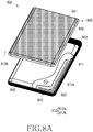
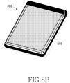
- FIGs. 8A and 8B illustrate a structure of an antenna device, 800, according to an embodiment of the present invention.
- the antenna device denoted by 800 includes a metallic case frame 830 for forming the appearance of a portable terminal, and a battery cover 840, a part of which is considered to form a portion of a first antenna element 810. That is, at least a portion of a metal surface 841 of the battery cover 840 acts as a portion of the first antenna element 810.
- a second portion of first antenna element 810 is a portion of the metallic case frame 830.
- the battery cover 840 is electrically coupled with the metallic case frame 830.
- a slot 812 consisting of slot components 812a and 812b is defined between a cut-out of a ground surface of a PCB 811, the battery cover 840 and the case frame 830.
- a second antenna element 820 is electromagnetically coupled to the first antenna element 810 via the slot 812 and resonates.
- PCB 811 transmits and receives RF signals to and from the second antenna element 820.
- the battery cover 840 is detachably mounted on the metallic case frame 830. When the battery cover 840 is combined with the metallic case frame 830, it is electrically connected with the metallic case frame 830 through a plurality of connector means 843 spaced apart.
- the battery cover 840 includes the metal part 841 and a nonmetal part 842. When the battery cover 840 and the metallic case frame 830 are combined, the nonmetal part 842 forms a portion of the slot 812. That is, the slot 812 is formed as a combination of a slot 812a cut out of the ground surface of PCB 811 and a slot 812b which is a portion of surface 842 overlaying the slot 812a.
- the second antenna element 820 receives RF power from the main board 811 and then resonates.
- the slot 812 is electromagnetically coupled with the second antenna element 820 and resonates due to the coupling.
- two or more metal members can be combined with each other and form a slot therebetween, which enables resonance and thus antenna radiation to be achieved.
- antenna devices according to embodiments of the present invention may implement resonance of a multi-band and a broadband.
- the antenna device may be applied to a portable terminal for a triple band or a quad-band.
- an antenna device may utilize a conventional metal member, which degrades antenna performance in prior art devices, as an active element of the antenna.
- antenna performance is enhanced, rather than degraded, with the use of the metal member.
Landscapes
- Engineering & Computer Science (AREA)
- Computer Networks & Wireless Communication (AREA)
- Support Of Aerials (AREA)
- Waveguide Aerials (AREA)
- Telephone Set Structure (AREA)
- Details Of Aerials (AREA)
Description
- The present disclosure relates generally to antennas, and more particularly, to a portable terminal comprising an antenna device.
- Portable (i.e., hand held) terminals such as mobile communication terminals (cellular phones), electronic schedulers, and personal complex terminals have become necessities of current society based on the recent technological advances in the telecommunications industry. The portable terminals have been developed into important means of information transmission, which are quickly changed.
- Recently, because modern portable terminals provide a variety of multimedia functions and have become smaller and lighter to enable convenient portability, usage has risen exponentially. However, it is becoming increasingly difficult to package a plurality of components within a limited space of the portable terminal. In general, the portable terminal has an antenna for wireless communication. Recently, the antenna is embedded in the portable terminal to beautify and miniaturize the portable terminal. It is preferable that the embedded antenna meets required performance metrics to smoothly transmit and receive signals in a corresponding communication service band.
- However, recently, use of a metal member for beautifying the appearance of the portable terminal or reinforcing rigidity of the portable terminal is increasing. There is a problem in that the metal member results in degradation of performance of the embedded antenna. Accordingly, there is a need for an antenna device to minimize or solve this problem.
-
WO 03/088414 - AMJAD A OMAR ET AL: "Design and Measurement of Self-Matched Dual-Frequency Coplanar Waveguide-Fed-Slot Antennas", IEEE TRANSACTIONS ON ANTENNAS AND PROPAGATION, IEEE SERVICE CENTER, PISCATAWAY, NJ, US, vol. 55, no. 1, 1 January 2007 (2007-01-01), pages 223-226, discloses two designs of dual frequency co-planar waveguide (CPW)-fed double folded slot antennas wherein the CPW is used to feed two double folded slot antennas of different bands resulting in dual band operation.
-
US 2008/106478 relates to broadband antennas and handheld electronic devices with broadband antennas. A handheld electronic device may have a housing in which electrical components such as integrated circuits and a broadband antenna are mounted. The broadband antenna may have a ground element and a resonating element. The resonating element may have two arms of unequal length and may have a self-resonant element. The antenna may have a feed terminal connected to the self-resonant element and a ground terminal connected to the ground element. The self-resonant element may be near-field coupled to one of the arms of the resonating element. With one suitable arrangement, the self-resonant element may be formed using a conductive rectangular element that is not electrically shorted to the ground element or the arms of the resonating element. The antenna may operate over first and second frequency ranges of interest. - An aspect of the present invention is to solve at least the above-mentioned problems and/or disadvantages and to provide at least the advantages described below. Accordingly, present invention relates to a portable terminal comprising an antenna device according to claim 1.
- The antenna device is inter alia comprised of first and second antenna elements. The first antenna element includes at least a portion of one or more metal members disposed within the portable terminal; is electrically connected with a ground surface of the PCB; and has a slot. The second antenna element, is disposed in proximity to the slot, spaced from and electromagnetically coupled to the first antenna element. The second antenna element receives RF power from the PCB and is configured to resonate at a frequency of the RF power.
- The above and other aspects, features and advantages of certain exemplary embodiments of the present invention will be more apparent from the following detailed description taken in conjunction with the accompanying drawings, in which:
-
FIG. 1 is a perspective view of a portable terminal according to one embodiment of the present invention; -
FIG. 2 illustrates a plan view / schematic diagram of an antenna device according to one example useful for understanding the invention; -
FIG. 3 illustrates a plan view / schematic diagram of an antenna device according to another example useful for understanding the invention; -
FIG. 4 illustrates a plan view / schematic diagram of an antenna device according to still another example useful for understanding the invention; -
FIG. 5 illustrates a variety of positions in which a slot can be located within an antenna device and portable terminal as an example useful for understanding the invention; -
FIG. 6 illustrates a planar structure of an antenna device according to one example useful for understanding the invention; -
FIG. 7 illustrates a further planar structure of an antenna device according to one example useful for understanding the invention; -
FIG. 8A illustrates a further planar structure of an antenna device according to one embodiment of the present invention; and -
FIG. 8B illustrates a further planar structure of an antenna device according to one embodiment of the present invention. - Exemplary embodiments of the present invention will be described herein below with reference to the accompanying drawings. In the following description, well-known functions or constructions are not described in detail since they would obscure the invention in unnecessary detail. Also, terms used herein should be understood in the context of the description of the exemplary embodiments Terms used may vary depending on user or operator intent and usage.
- The use of certain words and phrases used throughout this patent document should be understood as follows: the terms "include" and "comprise," as well as derivatives thereof, mean inclusion without limitation; the term "or," is inclusive, meaning and/or; the phrases "associated with" and "associated therewith," as well as derivatives thereof, may mean to include, be included within, interconnect with, contain, be contained within, connect to or with, couple to or with, be communicable with, cooperate with, interleave, juxtapose, be proximate to, be bound to or with, have, have a property of, or the like; the words "may" and "can" denote at least optional features, elements, functions, etc., for embodiments disclosed herein. If definitions for certain words and phrases are provided throughout this patent document, those of ordinary skill in the art should understand that in many, if not most instances, such definitions apply to prior, as well as future uses of such defined words and phrases.
- The present invention relates to an antenna device for securing antenna performance using one or more metal members installed in a portable terminal.
- Embodiments described hereinafter relate to an antenna device capable of securing antenna performance using one or more metal members installed for a corresponding purpose (e.g., for decoration) in a portable terminal. Embodiments enable a metal member installed in a portable terminal to enhance antenna performance rather than degrading antenna performance as in prior art designs. An antenna device according to one embodiment of the present invention may resonate with a slot which is formed in one or more metal members installed in a portable terminal or is formed by a combination of at least two of such metal members.
-
FIG. 1 is a perspective view of a portable terminal according to one embodiment of the present invention. - Here, the portable terminal is an example of an electronic device. Examples of a portable, i.e., hand held, electronic device include mobile phones, cellular phones and any portable device including a communication function.
- Referring to
FIG. 1 , the portable terminal denoted by 10 includes acase frame 11 for forming the appearance of the portable terminal 10 and components, described later, installed in thecase frame 11. The portable terminal 10 includes adisplay 12 for outputting images, aspeaker 13 for outputting sounds, amicrophone 14 for receiving sounds, and abutton 15. In addition, the portable terminal 10 may include a touch screen. Portable terminal 10 includes a PCB (not shown) upon which electronic components of terminal 10 are mounted. - Portable terminal 10 includes an antenna device for wireless communication, embodiments of which are described hereafter. The antenna device according to an embodiment is comprised of first and second antenna elements. The first antenna element includes at least a portion of one or more metal members disposed within the portable terminal. In one example, the one or more metal members is just a metal ground surface of the PCB.
- The first antenna element is electrically connected with the ground surface of the PCB. The first antenna element also has a slot. The second antenna element is disposed in proximity to the slot, and is spaced from and electromagnetically coupled to the first antenna element. The second antenna element receives RF power from an RF signal source mounted on the PCB, and is configured to resonate at a frequency of the RF power.
- The metal member may be a metal plate for reinforcing the PCB, a display unit, etc., a metal structure for supporting a battery, a case frame for beautifying the appearance of the portable terminal 10, etc.
- The second antenna element has a length sufficient to resonate at the RF frequency transmitted or received by the portable terminal. The first antenna element resonates by having sufficient length at the RF frequency and being electromagnetically coupled to the second antenna element. That is, the second antenna element is a parasitic element, and has current induced on the surface thereof by means of the electromagnetic coupling to the first antenna element.
- The slot may have a variety of shapes. For example, the slot may be L-shaped, a circle, a polygon, an elbow shape, etc. In addition, the slot may be filled with a dielectric or a magnetic material to improve radiation performance. The second antenna element may be a monopole antenna type or a loop antenna type or another suitable type.
-
FIG. 2 illustrates a structure of an antenna device according to one example. The antenna device denoted by 200 according to one example includes afirst antenna element 210 having aslot 212, and asecond antenna element 220 spaced from thefirst antenna element 210 and which is positioned within theslot 212 in this embodiment. A printed circuit board (PCB) 211 which may be the main PCB of portable device 10, is RF connected to thesecond antenna element 220 via a feed connector means 214, and thereby transmits RF power to thesecond antenna element 220 during a transmit mode. During a receive mode, thesecond antenna element 220 provides received RF power to a receiver (not shown) mounted onPCB 211. Thesecond antenna element 220 is of a sufficient length to resonate at the frequency of the RF power received from anRF signal source 213 of thePCB 211. - The RF frequency on transmit may be the same or nearly the same as the frequency of the RF signal in the receive mode. Further, operation of
antenna device 200 is preferable over a frequency band, and the length of thesecond antenna element 200 andslot 212 may be designed to achieve optimum resonance at the center of the band. Further, transmit and receive modes may occur simultaneously, and the transmit frequency band need not be the same as the receive frequency band, such that antenna performance parameters may be slightly different on transmit than on receive. (Note that ifantenna device 220 is used only for receiving, connection to theRF signal source 313 would not be necessary.) - The metal surface of the
first antenna element 210 surrounding theslot 212 of thefirst antenna element 210 is electromagnetically coupled with thesecond antenna element 220, whereby surface current is induced in thefirst antenna element 210. The slot is of sufficient length and shape to cause a resonance which produces radiation byantenna element 210 due to the induced surface current. Thus,first antenna element 210 is driven as a parasitic radiation element. Theslot 212 may have a thin and long groove shape. Thesecond antenna element 220 may have a shape in which it is positioned along a groove of theslot 212. The electromagnetically coupled quantity may be determined according to a shape and/or size of thesecond antenna element 220, distance in which thesecond antenna element 220 is spaced apart from theslot 212 edges, etc. An antenna matching according to the determined quantity can be determined. - The
first antenna element 210 may have theslot 212 in a single metal member itself, as illustrated inFIG. 2 . In other examples such as those described below, a slot may be defined by a space between a plurality of metal members. Examples of such metal members are a metal plate for reinforcingPCB 211 or a display unit, etc.; a metal structure for supporting a battery; a case frame equipped with a metal member for beautifying the appearance of the portable terminal, etc. For example, theslot 212 may be alternatively formed between a ground surface of thePCB 211 and a metal plate for supporting and reinforcing a display unit electrically connected with thePCB 211. - The
PCB 211 is equipped with theRF power source 213. Thesecond antenna element 220 and the RFpower supply part 213 are electrically connected through the RF feed connector means 214. ThePCB 211 is a board which mounts basic circuits and components. The components ofPCB 211 set an execution environment of the portable terminal and maintain the set information.PCB 211 allows the portable terminal 10 to be safely driven and smoothly performs data input and output of all devices of the portable terminal 10. - In the example of
FIG. 2 , thesecond antenna element 220 is L-shaped and theslot 212 is U-shaped. Further, the U-shape is asymmetrical, with a central portion and left and right side portions, where the left side portion (corresponding to the RF feed port end of second antenna element 220) is longer than the right side portion. As mentioned above, other suitable shapes and configurations for thesecond antenna element 220 and slot 212 are possible. - The
first antenna element 210 may be a part ofPCB 211 according to one example. This option is indicated schematically byconnection path 232. In general,PCB 211 includes the ground surface for reducing a harmful element such as noise. Theslot 212 may be formed as an aperture in this ground surface. In addition, thesecond antenna element 220 may be embodied as a monopole antenna which is electrically connected with theRF power source 213 at a feed port end thereof as shown, and which has no connection at the other end as shown inFIG. 2 . In an alternative configuration (not shown), thesecond antenna element 220 may be operated as a loop antenna which is RF connected with theRF power source 213 at the feed port one end and is electrically connected with the ground surface ofPCB 211 at the other end. - It is noted that while the
second antenna element 220 is shown unsupported within theslot 212, it is actually supported by a suitable support means (not shown) to maintain desired spacing from the metallic surfaces of thefirst antenna element 210. In the view ofFIG. 2 , the support means may be beneath thesecond antenna element 220, or may be provided via the RF connection means 214. Alternatively, a dielectric bonding agent (also not shown) may be used to attachsecond antenna element 220 tofirst antenna element 210 at various points. -
FIG. 3 illustrates a structure of an antenna device, 300, according to another example. This example differs from the example ofFIG. 2 in that the second antenna element is located outside the slot of the first antenna element, instead of inside the slot. - The
antenna device 300 includes afirst antenna element 310 having aslot 312, asecond antenna element 320 which is positioned out of theslot 312, and aPCB 311 which is RF connected with thesecond antenna element 320. Thesecond antenna element 320 receives RF power from anRF power source 313 and resonates at a frequency of the RF power. Theslot 312 of thefirst antenna element 310 is electromagnetically coupled with thesecond antenna element 320 and resonates due to such coupling. Thesecond antenna element 320 is spaced apart from thefirst antenna element 310 and, in this example has an L-shape configuration, which bends around the outside of thefirst antenna element 310 in proximity to theslot 312. Thesecond antenna element 320 is not limited to the L-shape. In the particular example ofFIG. 3 , theslot 312 is in the shape of an asymmetrical U, with a longer left side in proximity to anRF feed port 314 feeding an end of thesecond antenna element 320. Other shapes for theslot 312 are also possible.Second antenna element 320 is embodied as a monopole, and suitable support means (not shown) is provided in order to maintain desired spacing from thefirst antenna element 310 edges. The length ofsecond antenna element 320 is selected to achieve resonance over a desired frequency band or bands on transmit and/or receive. - Other elements and characteristics of
antenna device 300 are the same as corresponding elements ofantenna device 200 ofFIG. 2 , or ofantenna device 300 ofFIG. 3 ; thus a redundant discussion thereof is omitted. -
FIG. 4 illustrates a structure of an antenna device, 400, according to another example. The antenna device denoted by 400 includes afirst antenna element 410 having aslot 412, asecond antenna element 420 which is positioned outside of theslot 412, and aPCB 411 for transmitting and receiving an RF signal to and from thesecond antenna element 420. Thesecond antenna element 420 receives power from anRF power source 413, and resonates within a frequency band of the RF power. Theslot 412 of thefirst antenna element 410 is electromagnetically coupled with thesecond antenna element 420 and thereby resonates. - Particularly, the
antenna device 400 further includes a metallicexternal member 430 which surrounds thefirst antenna element 410 and thesecond antenna element 420 and insulates them from each other. Thesecond antenna element 420 is interposed between thefirst antenna element 410 and the metallicexternal member 430 and has a shape in which it is positioned along a groove of anotherslot 422 formed between the edges offirst antenna element 410 and theexternal member 430. - Other features and characteristics of
antenna device 400 are the same as corresponding features ofantenna device 200 ofFIG. 2 , thus a redundant discussion thereof is omitted. -
FIG. 5 illustrates a variety of positions in which a slot can be located within an antenna device and portable terminal. As shown inFIG. 5 , a slot which is formed in one metal member installed in a portable terminal or by combination of a plurality of metal members installed in the portable terminal may be formed in an upper part, a lower part, and a side part of the portable terminal. Particularly, it is preferable that the slot part is formed in a position where resonance a hand of a user, which holds the portable terminal, does not jam resonance of the slot. - In the illustrated examples, each of
first antenna elements 510a, 510b, 510c and 510b has an orientation corresponding to that of the portable terminal, with a top side T and a bottom side B. The top side T is located at the top portion of the portable terminal 10 including the speaker 13 (seeFIG. 1 ), and the bottom portion B is located at the bottom portion of the portable terminal housing themicrophone 14. As shown, the slots can be located substantially along either the left, right, top or bottom sides of the generally rectangular portable terminal. -
FIG. 6 illustrates a structure of an antenna device, 600, according to an example. A perspective view is shown in view (a); a plan view is illustrated in view (b). The antenna device denoted by 600 includes ametallic case frame 630 that forms part of the appearance of a portable terminal, and aPCB 611 which has aground surface 613 that also serves as the metal surface of thefirst antenna element 610. Thisground surface 613 is electrically connected to themetallic case frame 630 and includes aslot 612, asecond antenna element 620 which is positioned in theslot 612, and thePCB 611 for transmitting and receiving an RF signal to and from thesecond antenna element 620. - The
metallic case frame 630 and aground surface 613 ofPCB 611 together define theslot 612 therebetween. They are electrically connected through connector means 614, e.g., a plurality of spaced apart connectors. - The
PCB 611 is equipped with anRF power supply 615. Thesecond antenna element 620 is RF-connected with thepower supply 615 to receive RF power therefrom. Thesecond antenna element 610 resonates within a frequency band of the received RF power. In addition, thefirst antenna element 610 is electromagnetically coupled with thesecond antenna element 620 through theslot 612 and resonates due to the currents induced thereby. Theslot part 612 have a thin and long groove shape. Thesecond antenna element 620 may have a shape which is positioned along a groove of theslot 612. - The
second antenna element 620 may be mounted on thePCB 611, e.g., formed as a metal strip that runs along a dielectric surface of the PCB 111. However, thesecond antenna element 620 may alternatively be provided as an element that is separate fromPCB 611. - The
metallic case frame 630 can be electrically connected with not only theground surface 613 of themain board 611 but also a metal plate for reinforcing a display unit and/or a metal structure (e.g., a battery cover) for supporting a battery. Theslot 612 in this embodiment is formed between a portion of the inside surface ofcase frame 630, and an L shaped edge portion ofground surface 613, where the L-shaped edge is exposed due to an L-shaped cut-out along the perimeter ofground surface 613. Thus one side of theslot 612 abuts metal ofground surface 613 and the other side abuts metal ofcase frame 630. - The PCB611 is a board which mounts basic circuits and components.
PCB 611 includes electronics for setting an execution environment of the portable terminal and maintaining the set information.PCB 611 allows the portable terminal to be safely driven and smoothly performs data input and output of all devices of the portable terminal 10. -
FIG. 7 illustrates a structure of an antenna device, 700, according to still another example. View (a) depicts a perspective view and view (b) is a plan view. The antenna device denoted by 700 includes ametallic case frame 730 that forms part of the appearance of a portable terminal, aPCB 711 having aground surface 713 that is cut out to form aslot 712 entirely therein, and thereby form afirst antenna element 710 comprised of the portion of the metal surface surrounding theslot 712. Asecond antenna element 720 which is positioned within theslot 712, and thePCB 711 supplies RF power to thesecond antenna element 720. - The
metallic case frame 730 and aground surface 713 of themain board 711 are electrically connected through a plurality of spaced apart connector means 714. - The
PCB 711 is equipped with anRF power supply 715 which can be part of an RF communication unit (not shown) for modulating transmit signals and demodulating receive signals. Thesecond antenna element 720 is RF-connected with theRF power supply 715. Thesecond antenna element 720 receives RF power from theRF power supply 715 and resonates within a frequency band of the RF power. In addition, theslot 712 is electromagnetically coupled with thesecond antenna element 720 and resonates. Both thesecond antenna element 720 and theslot 712 can be L-shaped as shown. As illustrated, the slot can have a long side connecting at a right angle to a short side to form an L-shape, where the short side is tapered with a wider width at an end portion thereof. - The
second antenna element 720 may be mounted on thePCB 711, or it may alternatively be provided separate from PCB. -
FIGs. 8A and8B illustrate a structure of an antenna device, 800, according to an embodiment of the present invention. The antenna device denoted by 800 includes ametallic case frame 830 for forming the appearance of a portable terminal, and abattery cover 840, a part of which is considered to form a portion of afirst antenna element 810. That is, at least a portion of ametal surface 841 of thebattery cover 840 acts as a portion of thefirst antenna element 810. A second portion offirst antenna element 810 is a portion of themetallic case frame 830. Thebattery cover 840 is electrically coupled with themetallic case frame 830. Aslot 812 consisting ofslot components PCB 811, thebattery cover 840 and the case frame 830.Asecond antenna element 820 is electromagnetically coupled to thefirst antenna element 810 via theslot 812 and resonates.PCB 811 transmits and receives RF signals to and from thesecond antenna element 820. - The
battery cover 840 is detachably mounted on themetallic case frame 830. When thebattery cover 840 is combined with themetallic case frame 830, it is electrically connected with themetallic case frame 830 through a plurality of connector means 843 spaced apart. In addition, thebattery cover 840 includes themetal part 841 and anonmetal part 842. When thebattery cover 840 and themetallic case frame 830 are combined, thenonmetal part 842 forms a portion of theslot 812. That is, theslot 812 is formed as a combination of aslot 812a cut out of the ground surface ofPCB 811 and aslot 812b which is a portion ofsurface 842 overlaying theslot 812a. - The
second antenna element 820 receives RF power from themain board 811 and then resonates. Theslot 812 is electromagnetically coupled with thesecond antenna element 820 and resonates due to the coupling. - Accordingly, in some embodiments of the present invention, two or more metal members can be combined with each other and form a slot therebetween, which enables resonance and thus antenna radiation to be achieved.
- In addition, antenna devices according to embodiments of the present invention may implement resonance of a multi-band and a broadband. The antenna device may be applied to a portable terminal for a triple band or a quad-band.
- In conclusion, an antenna device according to the present invention may utilize a conventional metal member, which degrades antenna performance in prior art devices, as an active element of the antenna. Thus, antenna performance is enhanced, rather than degraded, with the use of the metal member.
- While the present invention has been particularly shown and described with reference to exemplary embodiments thereof, it will be understood by those skilled in the art that various changes in form and details may be made therein without departing from the scope of the present invention as defined by the appended claims.
Claims (8)
- A portable terminal comprising an antenna device (800) and a printed circuit board, PCB, (811) the antenna device comprising:a first antenna element (810) including at least a portion of one or more metal members (841, 830) disposed within the portable terminal, and electrically connected with a ground surface of the PCB, and having a slot (812); anda second antenna element (820), disposed in proximity to the slot, spaced from and electromagnetically coupled to the first antenna element, receiving RF power from the PCB via an electrical connection and configured to resonate at a frequency of the RF power; wherein the appearance of the portable terminal is formed at least partially by combination of a metallic front case frame (830) and a substantially metallic rear case frame (840), the first antenna element includes at least a portion of the front case frame and at least a portion of the rear case frame, and at least a portion of the slot (812) being formed between the front and rear case frames, wherein at least a part of the rear case frame is a battery cover, which is detachably mounted to the portable terminal and includes a metallic part (841) and a nonmetallic part (842), when the battery cover is attached to the portable terminal the metallic part is electrically connected to the front case frame, and wherein the slot is formed by a combination of a first slot (812a) cut out of a ground surface of the PCB, and a second slot (812b) formed by a first portion of the nonmetallic part of the battery cover overlaying the first slot (812a); wherein the slot (812) is electromagnetically coupled with the second antenna element and resonates due to the coupling.
- The antenna device of claim 1, wherein the second antenna element is disposed within the slot.
- The antenna device of claim 1, wherein the portable terminal has a top part including a speaker and a bottom part including a microphone, and the slot is formed in one of the upper part and the lower part.
- The antenna device of claim 1, wherein the portable terminal is generally rectangular with a top part including a speaker, a bottom part including a microphone, and left and right sides, and the slot is formed at least substantially along one of the left and right sides.
- The antenna device of claim 1, wherein the second antenna element is mounted on the printed circuit board.
- The antenna device of claim 1, wherein the second antenna element is a monopole that is RF connected at a feed port end thereof to a RF signal source of the PCB.
- The antenna device of claim 1, wherein the second antenna element is RF connected at a feed port end thereof to a RF signal source of the PCB, and is electrically connected with the ground surface of the PCB at an opposite end thereof.
- The antenna device of claim 1, wherein the second antenna element is L-shaped.
Applications Claiming Priority (1)
| Application Number | Priority Date | Filing Date | Title |
|---|---|---|---|
| KR1020120005898A KR101879705B1 (en) | 2012-01-18 | 2012-01-18 | Antenna apparatus for portable terminal |
Publications (3)
| Publication Number | Publication Date |
|---|---|
| EP2618423A2 EP2618423A2 (en) | 2013-07-24 |
| EP2618423A3 EP2618423A3 (en) | 2014-02-19 |
| EP2618423B1 true EP2618423B1 (en) | 2018-11-14 |
Family
ID=47458758
Family Applications (1)
| Application Number | Title | Priority Date | Filing Date |
|---|---|---|---|
| EP12199259.8A Not-in-force EP2618423B1 (en) | 2012-01-18 | 2012-12-21 | Antenna device for portable terminal |
Country Status (4)
| Country | Link |
|---|---|
| US (1) | US9190713B2 (en) |
| EP (1) | EP2618423B1 (en) |
| KR (1) | KR101879705B1 (en) |
| CN (1) | CN103219592B (en) |
Families Citing this family (47)
| Publication number | Priority date | Publication date | Assignee | Title |
|---|---|---|---|---|
| CN102738574B (en) | 2012-06-21 | 2014-09-03 | 华为终端有限公司 | Portable terminal and slot antenna thereof |
| TWI590525B (en) * | 2013-06-04 | 2017-07-01 | 群邁通訊股份有限公司 | Antenna structure and wireless communication device using the same |
| WO2015013880A1 (en) * | 2013-07-30 | 2015-02-05 | 华为终端有限公司 | Wireless terminal |
| TWI557990B (en) * | 2014-04-16 | 2016-11-11 | Mobile communication device | |
| US9608310B2 (en) * | 2014-05-23 | 2017-03-28 | Nokia Technologies Oy | Apparatus having a conductive housing and an antenna with tunable resonance |
| CN105281014B (en) * | 2014-06-20 | 2019-05-10 | 中兴通讯股份有限公司 | An antenna and terminal |
| TWM495681U (en) * | 2014-08-15 | 2015-02-11 | Wistron Neweb Corp | Wireless communication device |
| CN105449335A (en) * | 2014-08-20 | 2016-03-30 | 联想(北京)有限公司 | Electronic device |
| CN105514569A (en) * | 2014-09-23 | 2016-04-20 | 联想(北京)有限公司 | Electronic device |
| KR20160045312A (en) * | 2014-10-17 | 2016-04-27 | 삼성전자주식회사 | Antenna device and electronic device including the same |
| CN104269606B (en) * | 2014-10-24 | 2018-05-01 | 广东欧珀移动通信有限公司 | A kind of mobile terminal antenna structure and mobile terminal |
| CN105870625A (en) * | 2015-01-20 | 2016-08-17 | 中兴通讯股份有限公司 | Antenna design method, antenna and terminal |
| KR102231232B1 (en) | 2015-02-27 | 2021-03-23 | 삼성전자주식회사 | Antenna and electronic device having it |
| US10109914B2 (en) * | 2015-03-27 | 2018-10-23 | Intel IP Corporation | Antenna system |
| KR20170011340A (en) * | 2015-07-22 | 2017-02-02 | 삼성전자주식회사 | X-ray detector and x-ray imaging apparatus |
| KR101689612B1 (en) * | 2015-07-30 | 2016-12-26 | 엘지전자 주식회사 | Mobile terminal |
| CN106486757B (en) * | 2015-08-26 | 2021-01-15 | 小米科技有限责任公司 | Antenna, mobile terminal back cover and mobile terminal |
| CN106549208B (en) * | 2015-09-23 | 2019-07-05 | 宏达国际电子股份有限公司 | Electronic device |
| WO2017058178A1 (en) * | 2015-09-29 | 2017-04-06 | Hewlett-Packard Development Company, L.P. | Ground excitation antennas |
| US10290941B2 (en) * | 2016-01-27 | 2019-05-14 | Apple Inc. | Electronic device having multiband antenna with embedded filter |
| KR102465796B1 (en) * | 2016-05-27 | 2022-11-10 | 삼성전자주식회사 | Electronic device with multi-slot antenna |
| JP6642722B2 (en) * | 2016-08-25 | 2020-02-12 | 株式会社村田製作所 | Antenna device |
| EP3509161B1 (en) * | 2016-09-29 | 2021-11-10 | Huawei Technologies Co., Ltd. | Terminal |
| CN106357854B (en) * | 2016-11-04 | 2020-01-10 | Oppo广东移动通信有限公司 | Conductive cover body of mobile terminal, shell of mobile terminal and mobile terminal |
| US10103435B2 (en) * | 2016-11-09 | 2018-10-16 | Dell Products L.P. | Systems and methods for transloop impedance matching of an antenna |
| CN108281791B (en) * | 2017-01-05 | 2020-12-08 | 深圳富泰宏精密工业有限公司 | Electronic device |
| SG11201906237VA (en) * | 2017-01-24 | 2019-08-27 | Guangdong Oppo Mobile Telecommunications Corp Ltd | Blank assembly for housing, housing, manufacturing method for housing and terminal |
| TWI642230B (en) * | 2017-06-30 | 2018-11-21 | 宏碁股份有限公司 | Mobile device |
| CN108023981B (en) * | 2017-12-01 | 2020-08-04 | Oppo广东移动通信有限公司 | Middle frame assembly and electronic equipment |
| CN109904603B (en) * | 2017-12-07 | 2023-01-06 | 富泰华工业(深圳)有限公司 | Multi-band antenna and electronic device |
| CN108680797B (en) * | 2018-04-25 | 2022-02-08 | 歌尔股份有限公司 | Antenna test method and antenna test equipment |
| CN108808219B (en) * | 2018-05-25 | 2020-03-27 | 浙江大学 | Novel mobile device antenna |
| CN108736133A (en) * | 2018-07-13 | 2018-11-02 | Oppo广东移动通信有限公司 | antenna assembly and electronic device |
| DE102018122423A1 (en) | 2018-09-13 | 2020-03-19 | Endress+Hauser SE+Co. KG | Device for transmitting signals from an at least partially metallic housing |
| CN109597467B (en) | 2018-12-29 | 2021-07-16 | 联想(北京)有限公司 | Electronic equipment |
| TWI697151B (en) * | 2019-02-22 | 2020-06-21 | 啓碁科技股份有限公司 | Mobile device and antenna structure |
| TWI697152B (en) * | 2019-02-26 | 2020-06-21 | 啓碁科技股份有限公司 | Mobile device and antenna structure |
| TWI708427B (en) * | 2019-03-15 | 2020-10-21 | 廣達電腦股份有限公司 | Mobile device |
| DE102019108359A1 (en) * | 2019-03-30 | 2020-10-01 | Endress+Hauser SE+Co. KG | Device for transmitting signals from an at least partially metallic housing designed for use in a potentially explosive area |
| WO2021097783A1 (en) * | 2019-11-22 | 2021-05-27 | Goertek Technology Co., Ltd. | Antenna and wireless earbud comprising the same |
| TWI713254B (en) * | 2019-11-25 | 2020-12-11 | 和碩聯合科技股份有限公司 | Antenna module |
| CN117136472A (en) * | 2022-02-18 | 2023-11-28 | 广州视源电子科技股份有限公司 | An antenna assembly and interactive tablet |
| TWI814438B (en) * | 2022-06-10 | 2023-09-01 | 和碩聯合科技股份有限公司 | Electronic device |
| US20230411829A1 (en) * | 2022-06-20 | 2023-12-21 | Hewlett-Packard Development Company, L.P. | Antenna assemblies with printed circuit parasitic antenna elements |
| CN115589664A (en) * | 2022-09-24 | 2023-01-10 | 华为技术有限公司 | Electronic device |
| CN117438774B (en) * | 2023-11-17 | 2024-05-28 | 云谷(固安)科技有限公司 | Antenna assembly, housing and mobile terminal |
| US20250273846A1 (en) * | 2024-02-26 | 2025-08-28 | Google Llc | Parasitic Slots for Antenna Enhancement |
Family Cites Families (21)
| Publication number | Priority date | Publication date | Assignee | Title |
|---|---|---|---|---|
| FI113215B (en) * | 2001-05-17 | 2004-03-15 | Filtronic Lk Oy | The multiband antenna |
| JP4044302B2 (en) * | 2001-06-20 | 2008-02-06 | 株式会社村田製作所 | Surface mount type antenna and radio using the same |
| SE521833C2 (en) * | 2002-04-09 | 2003-12-09 | Moteco Ab | Antenna device comprising a non-galvanically coupled supply device |
| FI119667B (en) * | 2002-08-30 | 2009-01-30 | Pulse Finland Oy | Adjustable planar antenna |
| DE602006014003D1 (en) * | 2005-09-07 | 2010-06-10 | Thomson Licensing | COMPACT MULTI-BAND ANTENNA |
| US7616158B2 (en) * | 2006-05-26 | 2009-11-10 | Hong Kong Applied Science And Technology Research Institute Co., Ltd. | Multi mode antenna system |
| US20090273529A1 (en) * | 2006-09-12 | 2009-11-05 | Nxp, B.V. | Multiple antenna arrangement |
| US7688267B2 (en) | 2006-11-06 | 2010-03-30 | Apple Inc. | Broadband antenna with coupled feed for handheld electronic devices |
| US7764236B2 (en) * | 2007-01-04 | 2010-07-27 | Apple Inc. | Broadband antenna for handheld devices |
| US7612725B2 (en) | 2007-06-21 | 2009-11-03 | Apple Inc. | Antennas for handheld electronic devices with conductive bezels |
| US8188929B2 (en) | 2008-05-29 | 2012-05-29 | Motorola Mobility, Inc. | Self-resonating antenna |
| US8665164B2 (en) * | 2008-11-19 | 2014-03-04 | Apple Inc. | Multiband handheld electronic device slot antenna |
| US8085202B2 (en) * | 2009-03-17 | 2011-12-27 | Research In Motion Limited | Wideband, high isolation two port antenna array for multiple input, multiple output handheld devices |
| US8269675B2 (en) | 2009-06-23 | 2012-09-18 | Apple Inc. | Antennas for electronic devices with conductive housing |
| US8587491B2 (en) * | 2009-07-17 | 2013-11-19 | Blackberry Limited | Antenna with a C-shaped slot nested within an L-shaped slot and mobile device employing the antenna |
| US8576561B2 (en) * | 2010-02-02 | 2013-11-05 | Apple Inc. | Handheld device enclosure |
| US8698677B2 (en) * | 2010-04-09 | 2014-04-15 | Sony Corporation | Mobile wireless terminal and antenna device |
| TWI411165B (en) * | 2010-10-22 | 2013-10-01 | Acer Inc | Mobile communication device and antenna |
| JP2012142793A (en) * | 2010-12-28 | 2012-07-26 | Fujitsu Component Ltd | Antenna device |
| KR101779457B1 (en) | 2011-04-22 | 2017-09-19 | 삼성전자주식회사 | Antenna device for portable terminal |
| KR101787384B1 (en) | 2011-06-10 | 2017-10-20 | 삼성전자주식회사 | Antenna apparatus for portable terminal |
-
2012
- 2012-01-18 KR KR1020120005898A patent/KR101879705B1/en active Active
- 2012-09-14 US US13/616,072 patent/US9190713B2/en active Active
- 2012-12-12 CN CN201210536305.5A patent/CN103219592B/en not_active Expired - Fee Related
- 2012-12-21 EP EP12199259.8A patent/EP2618423B1/en not_active Not-in-force
Non-Patent Citations (1)
| Title |
|---|
| None * |
Also Published As
| Publication number | Publication date |
|---|---|
| US9190713B2 (en) | 2015-11-17 |
| CN103219592B (en) | 2017-11-17 |
| US20130181871A1 (en) | 2013-07-18 |
| KR20130084931A (en) | 2013-07-26 |
| CN103219592A (en) | 2013-07-24 |
| KR101879705B1 (en) | 2018-07-18 |
| EP2618423A3 (en) | 2014-02-19 |
| EP2618423A2 (en) | 2013-07-24 |
Similar Documents
| Publication | Publication Date | Title |
|---|---|---|
| US9190713B2 (en) | Antenna device for portable terminal | |
| KR101547746B1 (en) | Chassis-excited antenna component, antenna apparatus, and mobile communications device thereof | |
| CN113517556B (en) | Antenna structure and electronic equipment with same | |
| KR101787384B1 (en) | Antenna apparatus for portable terminal | |
| US9281553B2 (en) | Wearable device | |
| US9673507B2 (en) | Chassis-excited antenna apparatus and methods | |
| TWI691117B (en) | Antenna structure and wireless communication device using the same | |
| CN102738556B (en) | Antenna device for portable terminal and portable terminal with antenna device | |
| JP4358084B2 (en) | Foldable portable radio | |
| CN107645040B (en) | Antenna structure and wireless communication device with same | |
| EP1305843B1 (en) | Antenna arrangement and portable radio communication device | |
| CN1879256B (en) | Antenna, manufacturing method thereof, and portable wireless terminal using the same | |
| US7161541B2 (en) | Mobile telecommunication device and planar antenna thereof | |
| WO2007058230A1 (en) | Slot antenna and portable wireless terminal | |
| JPWO2007043138A1 (en) | Folding portable wireless device | |
| JP4227141B2 (en) | Antenna device | |
| EP2375488B1 (en) | Planar antenna and handheld device | |
| EP1641077A1 (en) | Mobile telecommunication device and planar antenna therefor | |
| WO2010067479A1 (en) | Portable wireless apparatus | |
| KR101589066B1 (en) | Antenna apparatus for portable terminal | |
| TWI508372B (en) | Antenna structure and wireless communication device using the same | |
| CN121965108A (en) | Electronic equipment | |
| JP2007150863A (en) | Device with radio communication function | |
| WO2014002378A1 (en) | Antenna device and portable radio equipment | |
| WO2012053196A1 (en) | Antenna device |
Legal Events
| Date | Code | Title | Description |
|---|---|---|---|
| PUAI | Public reference made under article 153(3) epc to a published international application that has entered the european phase |
Free format text: ORIGINAL CODE: 0009012 |
|
| AK | Designated contracting states |
Kind code of ref document: A2 Designated state(s): AL AT BE BG CH CY CZ DE DK EE ES FI FR GB GR HR HU IE IS IT LI LT LU LV MC MK MT NL NO PL PT RO RS SE SI SK SM TR |
|
| AX | Request for extension of the european patent |
Extension state: BA ME |
|
| PUAL | Search report despatched |
Free format text: ORIGINAL CODE: 0009013 |
|
| AK | Designated contracting states |
Kind code of ref document: A3 Designated state(s): AL AT BE BG CH CY CZ DE DK EE ES FI FR GB GR HR HU IE IS IT LI LT LU LV MC MK MT NL NO PL PT RO RS SE SI SK SM TR |
|
| AX | Request for extension of the european patent |
Extension state: BA ME |
|
| RIC1 | Information provided on ipc code assigned before grant |
Ipc: H01Q 9/42 20060101ALI20140116BHEP Ipc: H01Q 1/24 20060101AFI20140116BHEP Ipc: H01Q 5/00 20060101ALI20140116BHEP Ipc: H01Q 13/10 20060101ALI20140116BHEP |
|
| 17P | Request for examination filed |
Effective date: 20140815 |
|
| RBV | Designated contracting states (corrected) |
Designated state(s): AL AT BE BG CH CY CZ DE DK EE ES FI FR GB GR HR HU IE IS IT LI LT LU LV MC MK MT NL NO PL PT RO RS SE SI SK SM TR |
|
| 17Q | First examination report despatched |
Effective date: 20160829 |
|
| APBK | Appeal reference recorded |
Free format text: ORIGINAL CODE: EPIDOSNREFNE |
|
| APBN | Date of receipt of notice of appeal recorded |
Free format text: ORIGINAL CODE: EPIDOSNNOA2E |
|
| APBR | Date of receipt of statement of grounds of appeal recorded |
Free format text: ORIGINAL CODE: EPIDOSNNOA3E |
|
| APBV | Interlocutory revision of appeal recorded |
Free format text: ORIGINAL CODE: EPIDOSNIRAPE |
|
| GRAP | Despatch of communication of intention to grant a patent |
Free format text: ORIGINAL CODE: EPIDOSNIGR1 |
|
| INTG | Intention to grant announced |
Effective date: 20180719 |
|
| GRAS | Grant fee paid |
Free format text: ORIGINAL CODE: EPIDOSNIGR3 |
|
| GRAA | (expected) grant |
Free format text: ORIGINAL CODE: 0009210 |
|
| AK | Designated contracting states |
Kind code of ref document: B1 Designated state(s): AL AT BE BG CH CY CZ DE DK EE ES FI FR GB GR HR HU IE IS IT LI LT LU LV MC MK MT NL NO PL PT RO RS SE SI SK SM TR |
|
| REG | Reference to a national code |
Ref country code: CH Ref legal event code: EP Ref country code: AT Ref legal event code: REF Ref document number: 1065924 Country of ref document: AT Kind code of ref document: T Effective date: 20181115 |
|
| REG | Reference to a national code |
Ref country code: DE Ref legal event code: R096 Ref document number: 602012053421 Country of ref document: DE |
|
| REG | Reference to a national code |
Ref country code: IE Ref legal event code: FG4D |
|
| REG | Reference to a national code |
Ref country code: NL Ref legal event code: FP |
|
| REG | Reference to a national code |
Ref country code: LT Ref legal event code: MG4D |
|
| REG | Reference to a national code |
Ref country code: AT Ref legal event code: MK05 Ref document number: 1065924 Country of ref document: AT Kind code of ref document: T Effective date: 20181114 |
|
| PG25 | Lapsed in a contracting state [announced via postgrant information from national office to epo] |
Ref country code: FI Free format text: LAPSE BECAUSE OF FAILURE TO SUBMIT A TRANSLATION OF THE DESCRIPTION OR TO PAY THE FEE WITHIN THE PRESCRIBED TIME-LIMIT Effective date: 20181114 Ref country code: BG Free format text: LAPSE BECAUSE OF FAILURE TO SUBMIT A TRANSLATION OF THE DESCRIPTION OR TO PAY THE FEE WITHIN THE PRESCRIBED TIME-LIMIT Effective date: 20190214 Ref country code: HR Free format text: LAPSE BECAUSE OF FAILURE TO SUBMIT A TRANSLATION OF THE DESCRIPTION OR TO PAY THE FEE WITHIN THE PRESCRIBED TIME-LIMIT Effective date: 20181114 Ref country code: LV Free format text: LAPSE BECAUSE OF FAILURE TO SUBMIT A TRANSLATION OF THE DESCRIPTION OR TO PAY THE FEE WITHIN THE PRESCRIBED TIME-LIMIT Effective date: 20181114 Ref country code: AT Free format text: LAPSE BECAUSE OF FAILURE TO SUBMIT A TRANSLATION OF THE DESCRIPTION OR TO PAY THE FEE WITHIN THE PRESCRIBED TIME-LIMIT Effective date: 20181114 Ref country code: LT Free format text: LAPSE BECAUSE OF FAILURE TO SUBMIT A TRANSLATION OF THE DESCRIPTION OR TO PAY THE FEE WITHIN THE PRESCRIBED TIME-LIMIT Effective date: 20181114 Ref country code: ES Free format text: LAPSE BECAUSE OF FAILURE TO SUBMIT A TRANSLATION OF THE DESCRIPTION OR TO PAY THE FEE WITHIN THE PRESCRIBED TIME-LIMIT Effective date: 20181114 Ref country code: NO Free format text: LAPSE BECAUSE OF FAILURE TO SUBMIT A TRANSLATION OF THE DESCRIPTION OR TO PAY THE FEE WITHIN THE PRESCRIBED TIME-LIMIT Effective date: 20190214 Ref country code: IS Free format text: LAPSE BECAUSE OF FAILURE TO SUBMIT A TRANSLATION OF THE DESCRIPTION OR TO PAY THE FEE WITHIN THE PRESCRIBED TIME-LIMIT Effective date: 20190314 |
|
| PG25 | Lapsed in a contracting state [announced via postgrant information from national office to epo] |
Ref country code: PT Free format text: LAPSE BECAUSE OF FAILURE TO SUBMIT A TRANSLATION OF THE DESCRIPTION OR TO PAY THE FEE WITHIN THE PRESCRIBED TIME-LIMIT Effective date: 20190314 Ref country code: AL Free format text: LAPSE BECAUSE OF FAILURE TO SUBMIT A TRANSLATION OF THE DESCRIPTION OR TO PAY THE FEE WITHIN THE PRESCRIBED TIME-LIMIT Effective date: 20181114 Ref country code: GR Free format text: LAPSE BECAUSE OF FAILURE TO SUBMIT A TRANSLATION OF THE DESCRIPTION OR TO PAY THE FEE WITHIN THE PRESCRIBED TIME-LIMIT Effective date: 20190215 Ref country code: RS Free format text: LAPSE BECAUSE OF FAILURE TO SUBMIT A TRANSLATION OF THE DESCRIPTION OR TO PAY THE FEE WITHIN THE PRESCRIBED TIME-LIMIT Effective date: 20181114 Ref country code: SE Free format text: LAPSE BECAUSE OF FAILURE TO SUBMIT A TRANSLATION OF THE DESCRIPTION OR TO PAY THE FEE WITHIN THE PRESCRIBED TIME-LIMIT Effective date: 20181114 |
|
| PG25 | Lapsed in a contracting state [announced via postgrant information from national office to epo] |
Ref country code: CZ Free format text: LAPSE BECAUSE OF FAILURE TO SUBMIT A TRANSLATION OF THE DESCRIPTION OR TO PAY THE FEE WITHIN THE PRESCRIBED TIME-LIMIT Effective date: 20181114 Ref country code: IT Free format text: LAPSE BECAUSE OF FAILURE TO SUBMIT A TRANSLATION OF THE DESCRIPTION OR TO PAY THE FEE WITHIN THE PRESCRIBED TIME-LIMIT Effective date: 20181114 Ref country code: DK Free format text: LAPSE BECAUSE OF FAILURE TO SUBMIT A TRANSLATION OF THE DESCRIPTION OR TO PAY THE FEE WITHIN THE PRESCRIBED TIME-LIMIT Effective date: 20181114 Ref country code: PL Free format text: LAPSE BECAUSE OF FAILURE TO SUBMIT A TRANSLATION OF THE DESCRIPTION OR TO PAY THE FEE WITHIN THE PRESCRIBED TIME-LIMIT Effective date: 20181114 |
|
| REG | Reference to a national code |
Ref country code: CH Ref legal event code: PL |
|
| REG | Reference to a national code |
Ref country code: DE Ref legal event code: R097 Ref document number: 602012053421 Country of ref document: DE |
|
| PG25 | Lapsed in a contracting state [announced via postgrant information from national office to epo] |
Ref country code: EE Free format text: LAPSE BECAUSE OF FAILURE TO SUBMIT A TRANSLATION OF THE DESCRIPTION OR TO PAY THE FEE WITHIN THE PRESCRIBED TIME-LIMIT Effective date: 20181114 Ref country code: SM Free format text: LAPSE BECAUSE OF FAILURE TO SUBMIT A TRANSLATION OF THE DESCRIPTION OR TO PAY THE FEE WITHIN THE PRESCRIBED TIME-LIMIT Effective date: 20181114 Ref country code: SK Free format text: LAPSE BECAUSE OF FAILURE TO SUBMIT A TRANSLATION OF THE DESCRIPTION OR TO PAY THE FEE WITHIN THE PRESCRIBED TIME-LIMIT Effective date: 20181114 Ref country code: MC Free format text: LAPSE BECAUSE OF FAILURE TO SUBMIT A TRANSLATION OF THE DESCRIPTION OR TO PAY THE FEE WITHIN THE PRESCRIBED TIME-LIMIT Effective date: 20181114 Ref country code: LU Free format text: LAPSE BECAUSE OF NON-PAYMENT OF DUE FEES Effective date: 20181221 Ref country code: RO Free format text: LAPSE BECAUSE OF FAILURE TO SUBMIT A TRANSLATION OF THE DESCRIPTION OR TO PAY THE FEE WITHIN THE PRESCRIBED TIME-LIMIT Effective date: 20181114 |
|
| REG | Reference to a national code |
Ref country code: IE Ref legal event code: MM4A |
|
| PLBE | No opposition filed within time limit |
Free format text: ORIGINAL CODE: 0009261 |
|
| STAA | Information on the status of an ep patent application or granted ep patent |
Free format text: STATUS: NO OPPOSITION FILED WITHIN TIME LIMIT |
|
| REG | Reference to a national code |
Ref country code: BE Ref legal event code: MM Effective date: 20181231 |
|
| 26N | No opposition filed |
Effective date: 20190815 |
|
| PG25 | Lapsed in a contracting state [announced via postgrant information from national office to epo] |
Ref country code: SI Free format text: LAPSE BECAUSE OF FAILURE TO SUBMIT A TRANSLATION OF THE DESCRIPTION OR TO PAY THE FEE WITHIN THE PRESCRIBED TIME-LIMIT Effective date: 20181114 Ref country code: IE Free format text: LAPSE BECAUSE OF NON-PAYMENT OF DUE FEES Effective date: 20181221 Ref country code: FR Free format text: LAPSE BECAUSE OF NON-PAYMENT OF DUE FEES Effective date: 20190114 |
|
| PG25 | Lapsed in a contracting state [announced via postgrant information from national office to epo] |
Ref country code: BE Free format text: LAPSE BECAUSE OF NON-PAYMENT OF DUE FEES Effective date: 20181231 |
|
| PG25 | Lapsed in a contracting state [announced via postgrant information from national office to epo] |
Ref country code: LI Free format text: LAPSE BECAUSE OF NON-PAYMENT OF DUE FEES Effective date: 20181231 Ref country code: CH Free format text: LAPSE BECAUSE OF NON-PAYMENT OF DUE FEES Effective date: 20181231 |
|
| PG25 | Lapsed in a contracting state [announced via postgrant information from national office to epo] |
Ref country code: MT Free format text: LAPSE BECAUSE OF NON-PAYMENT OF DUE FEES Effective date: 20181221 |
|
| PG25 | Lapsed in a contracting state [announced via postgrant information from national office to epo] |
Ref country code: TR Free format text: LAPSE BECAUSE OF FAILURE TO SUBMIT A TRANSLATION OF THE DESCRIPTION OR TO PAY THE FEE WITHIN THE PRESCRIBED TIME-LIMIT Effective date: 20181114 |
|
| PG25 | Lapsed in a contracting state [announced via postgrant information from national office to epo] |
Ref country code: CY Free format text: LAPSE BECAUSE OF FAILURE TO SUBMIT A TRANSLATION OF THE DESCRIPTION OR TO PAY THE FEE WITHIN THE PRESCRIBED TIME-LIMIT Effective date: 20181114 Ref country code: MK Free format text: LAPSE BECAUSE OF NON-PAYMENT OF DUE FEES Effective date: 20181114 Ref country code: HU Free format text: LAPSE BECAUSE OF FAILURE TO SUBMIT A TRANSLATION OF THE DESCRIPTION OR TO PAY THE FEE WITHIN THE PRESCRIBED TIME-LIMIT; INVALID AB INITIO Effective date: 20121221 |
|
| PGFP | Annual fee paid to national office [announced via postgrant information from national office to epo] |
Ref country code: NL Payment date: 20201123 Year of fee payment: 9 |
|
| PGFP | Annual fee paid to national office [announced via postgrant information from national office to epo] |
Ref country code: DE Payment date: 20201120 Year of fee payment: 9 Ref country code: GB Payment date: 20201125 Year of fee payment: 9 |
|
| REG | Reference to a national code |
Ref country code: DE Ref legal event code: R119 Ref document number: 602012053421 Country of ref document: DE |
|
| REG | Reference to a national code |
Ref country code: NL Ref legal event code: MM Effective date: 20220101 |
|
| GBPC | Gb: european patent ceased through non-payment of renewal fee |
Effective date: 20211221 |
|
| PG25 | Lapsed in a contracting state [announced via postgrant information from national office to epo] |
Ref country code: NL Free format text: LAPSE BECAUSE OF NON-PAYMENT OF DUE FEES Effective date: 20220101 |
|
| PG25 | Lapsed in a contracting state [announced via postgrant information from national office to epo] |
Ref country code: GB Free format text: LAPSE BECAUSE OF NON-PAYMENT OF DUE FEES Effective date: 20211221 Ref country code: DE Free format text: LAPSE BECAUSE OF NON-PAYMENT OF DUE FEES Effective date: 20220701 |