EP2615611A2 - Multi-mode memory device and method - Google Patents
Multi-mode memory device and method Download PDFInfo
- Publication number
- EP2615611A2 EP2615611A2 EP13157772.8A EP13157772A EP2615611A2 EP 2615611 A2 EP2615611 A2 EP 2615611A2 EP 13157772 A EP13157772 A EP 13157772A EP 2615611 A2 EP2615611 A2 EP 2615611A2
- Authority
- EP
- European Patent Office
- Prior art keywords
- memory device
- command
- memory
- address
- logic die
- Prior art date
- Legal status (The legal status is an assumption and is not a legal conclusion. Google has not performed a legal analysis and makes no representation as to the accuracy of the status listed.)
- Granted
Links
Images




Classifications
-
- G—PHYSICS
- G11—INFORMATION STORAGE
- G11C—STATIC STORES
- G11C11/00—Digital stores characterised by the use of particular electric or magnetic storage elements; Storage elements therefor
- G11C11/21—Digital stores characterised by the use of particular electric or magnetic storage elements; Storage elements therefor using electric elements
- G11C11/34—Digital stores characterised by the use of particular electric or magnetic storage elements; Storage elements therefor using electric elements using semiconductor devices
- G11C11/40—Digital stores characterised by the use of particular electric or magnetic storage elements; Storage elements therefor using electric elements using semiconductor devices using transistors
- G11C11/401—Digital stores characterised by the use of particular electric or magnetic storage elements; Storage elements therefor using electric elements using semiconductor devices using transistors forming cells needing refreshing or charge regeneration, i.e. dynamic cells
- G11C11/4063—Auxiliary circuits, e.g. for addressing, decoding, driving, writing, sensing or timing
- G11C11/407—Auxiliary circuits, e.g. for addressing, decoding, driving, writing, sensing or timing for memory cells of the field-effect type
- G11C11/408—Address circuits
-
- G—PHYSICS
- G11—INFORMATION STORAGE
- G11C—STATIC STORES
- G11C11/00—Digital stores characterised by the use of particular electric or magnetic storage elements; Storage elements therefor
- G11C11/21—Digital stores characterised by the use of particular electric or magnetic storage elements; Storage elements therefor using electric elements
- G11C11/34—Digital stores characterised by the use of particular electric or magnetic storage elements; Storage elements therefor using electric elements using semiconductor devices
- G11C11/40—Digital stores characterised by the use of particular electric or magnetic storage elements; Storage elements therefor using electric elements using semiconductor devices using transistors
- G11C11/401—Digital stores characterised by the use of particular electric or magnetic storage elements; Storage elements therefor using electric elements using semiconductor devices using transistors forming cells needing refreshing or charge regeneration, i.e. dynamic cells
- G11C11/4063—Auxiliary circuits, e.g. for addressing, decoding, driving, writing, sensing or timing
- G11C11/407—Auxiliary circuits, e.g. for addressing, decoding, driving, writing, sensing or timing for memory cells of the field-effect type
- G11C11/409—Read-write [R-W] circuits
- G11C11/4093—Input/output [I/O] data interface arrangements, e.g. data buffers
-
- G—PHYSICS
- G06—COMPUTING OR CALCULATING; COUNTING
- G06F—ELECTRIC DIGITAL DATA PROCESSING
- G06F13/00—Interconnection of, or transfer of information or other signals between, memories, input/output devices or central processing units
- G06F13/14—Handling requests for interconnection or transfer
- G06F13/16—Handling requests for interconnection or transfer for access to memory bus
- G06F13/1668—Details of memory controller
- G06F13/1694—Configuration of memory controller to different memory types
-
- G—PHYSICS
- G11—INFORMATION STORAGE
- G11C—STATIC STORES
- G11C11/00—Digital stores characterised by the use of particular electric or magnetic storage elements; Storage elements therefor
- G11C11/21—Digital stores characterised by the use of particular electric or magnetic storage elements; Storage elements therefor using electric elements
- G11C11/34—Digital stores characterised by the use of particular electric or magnetic storage elements; Storage elements therefor using electric elements using semiconductor devices
- G11C11/40—Digital stores characterised by the use of particular electric or magnetic storage elements; Storage elements therefor using electric elements using semiconductor devices using transistors
- G11C11/401—Digital stores characterised by the use of particular electric or magnetic storage elements; Storage elements therefor using electric elements using semiconductor devices using transistors forming cells needing refreshing or charge regeneration, i.e. dynamic cells
- G11C11/4063—Auxiliary circuits, e.g. for addressing, decoding, driving, writing, sensing or timing
- G11C11/407—Auxiliary circuits, e.g. for addressing, decoding, driving, writing, sensing or timing for memory cells of the field-effect type
- G11C11/409—Read-write [R-W] circuits
-
- G—PHYSICS
- G11—INFORMATION STORAGE
- G11C—STATIC STORES
- G11C11/00—Digital stores characterised by the use of particular electric or magnetic storage elements; Storage elements therefor
- G11C11/21—Digital stores characterised by the use of particular electric or magnetic storage elements; Storage elements therefor using electric elements
- G11C11/34—Digital stores characterised by the use of particular electric or magnetic storage elements; Storage elements therefor using electric elements using semiconductor devices
- G11C11/40—Digital stores characterised by the use of particular electric or magnetic storage elements; Storage elements therefor using electric elements using semiconductor devices using transistors
- G11C11/401—Digital stores characterised by the use of particular electric or magnetic storage elements; Storage elements therefor using electric elements using semiconductor devices using transistors forming cells needing refreshing or charge regeneration, i.e. dynamic cells
- G11C11/4063—Auxiliary circuits, e.g. for addressing, decoding, driving, writing, sensing or timing
- G11C11/407—Auxiliary circuits, e.g. for addressing, decoding, driving, writing, sensing or timing for memory cells of the field-effect type
- G11C11/409—Read-write [R-W] circuits
- G11C11/4096—Input/output [I/O] data management or control circuits, e.g. reading or writing circuits, I/O drivers or bit-line switches
-
- G—PHYSICS
- G11—INFORMATION STORAGE
- G11C—STATIC STORES
- G11C5/00—Details of stores covered by group G11C11/00
- G11C5/02—Disposition of storage elements, e.g. in the form of a matrix array
Definitions
- Embodiments of the invention relate to memory devices, and, more particularly, in one or more embodiments to a memory device that can be operated in either a direct mode, in which conventional memory control signals are coupled to the memory devices, or an indirect mode, in which command packets are coupled to the memory devices.
- DRAM dynamic random access memory
- Figure 1 is a block diagram of a computer system that includes a dual mode memory system according to an embodiment of the invention.
- Figure 2 is a block diagram of a dual mode memory system according to an embodiment of the invention.
- FIG. 3 is a more detailed block diagram of a dual mode memory system according to an embodiment of the invention.
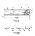
- Figure 4 is a packet diagram showing the format of a downstream packet that can be coupled to the memory system of Figures 1 , 2 or 3 or a memory system according to some other embodiment of the invention for the indirect operating mode.
- Figure 5 is a chart showing how the commands in the first field of the downstream packet of Figure 4 are modified for the direct operating mode.
- Figure 6 is a chart showing the commands in the downstream packet of Figure 4 for the indirect operating mode.
- Figure 7 is a packet diagram showing the format of an upstream packet that can be coupled from the memory system of Figures 1 , 2 or 3 or a memory system according to some other embodiment of the invention.
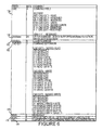
- Figure 8 is a chart showing the commands in the upstream packet of Figure 7 for the indirect operating mode.
- a computer system including a high-capacity, high bandwidth memory device 10 is shown in Figure 1 connected to a processor 12 through a relatively narrow high-speed bus 14 that may be divided into downstream lanes and separate upstream lanes (not shown in Figure 1 ).
- the memory device 10 includes 4 DRAM die 20, 22, 24, 26, which may be identical to each other, stacked on top of each other. Although the memory device 10 includes 4 DRAM die 20, 22, 24, 26, other embodiments of the memory device use a greater or lesser number of DRAM die.
- the DRAM die 20, 22, 24, 26 are stacked with (e.g., on top of) a logic die 30, which serves as the interface with the processor 12.
- the logic die 30 can implement a variety of functions in the memory device 10, such as to limit the number of functions that are be implemented in the DRAM die 20; 22, 24, 26.
- the logic die 30 may perform memory management functions, such as power management and refresh of memory cells in the DRAM die 20, 22, 24, 26.
- the logic die 30 may implement test and/or repair capabilities, and it may perform error checking and correcting ("ECC") functions.
- ECC error checking and correcting
- the DRAM die 20, 22, 24, 26 are connected to each other and to the logic die 30 by a relatively wide bus 34.
- the bus 34 may be implemented with through silicon vias ("TSVs"), which comprise a large number of conductors extending through the DRAM die 20, 22, 24, 26 at the same locations on the DRAM die and connect to respective conductors formed on the die 20, 22, 24, 26.
- TSVs through silicon vias
- each of the DRAM die 20, 22, 24, 26 are divided into 16 autonomous partitions, each of which may contain 2 or 4 independent memory banks.
- the partitions of each die 20, 22, 24, 26 that are stacked on top of each other may be independently accessed for read and write operations.
- Each set of 16 stacked partitions may be referred to as a "vault.”
- the memory device 10 may contain 16 vaults.
- the bus 34 may be divided into 16 36-bit bi-directional sub-buses 38a-p, with each of the 16 36-bit sub-buses coupled to the 4 partitions in a respective vault.
- Each of these sub-buses couples 32 bits of a data and 4 ECC bits between the logic die 30 and the DRAM die 20, 22, 24, 26.
- the number of stacked DRAM die 20, 22, 24, 26, the number of partitions in each DRAM die, the number of banks in each partition, and the number of bits in each of the sub-buses 38a-p can vary as desired.
- the relatively narrow high-speed bus 14 connecting the processor 12 to the logic die may be divided into 4 16-bit downstream lanes 40a-d and 4 separate 16-bit upstream lanes 42a-d.
- the 4 downstream lanes 40a-d may be connected to a single processor 12 as shown in Figure 1 , which may be a multi-core processor, to multiple processors (not shown), or to some other memory access device like a memory controller.
- the 4 downstream lanes 40a-d may operate independently of each other so that packets (in the indirect mode) or memory command, address, and data signals (in the direct mode) are coupled through the lanes 40a-d at different times and to the same or different vaults.
- one of the functions performed by the logic die 30 can be to serialize the read data bits coupled from the DRAM die 20, 22, 24, 26 into a serial stream of 16 serial data bits coupled through 16 parallel bits of each upstream lane 42a-d of the bus 14.
- the logic die 30 may perform the functions of deserializing 16 serial data bits coupled through one of the 16-bit downstream lanes 40a-d of the bus 14 to obtain 256 parallel data bits.
- the logic die 30 then couples these 256 bits through one of the 32-bit sub-buses 38a-p in a serial stream of 8 bits.
- other embodiments may use different numbers of lanes 40, 42 having different widths or different numbers of sub-buses 38a-p having different widths, and they may couple data bits having different structures.
- the stacking of multiple DRAM die results in a memory device having a very large capacity.
- the use of a very wide bus connecting the DRAM die allows data to be coupled to and from the DRAM die with a very high bandwidth.
- a logic die 30 is shown in Figure 3 connected to the processor 12 and the DRAM die 20, 22, 24, 26.
- each of the 4 downstream lanes 40a-d may be connected to a respective link interface 50a-d.
- Each link interface 50a-d includes a deserializer 54 that converts each serial stream of 16 data bits on each of the 16-bit lanes 40a-d to 256 parallel bits. Insofar as there are 4 link interfaces 50a-d, the link interfaces can together output 1024 output parallel bits.
- Each of the link interfaces 50a-d applies its 256 parallel bits to a respective downstream target 60a-d, which decodes the command and address portions of the received packet (in the indirect mode) or the commands and addresses (in the direct mode) and buffers write data in the event a memory request is for a write operation.
- the downstream targets 60a-d output their respective commands, addresses and possibly write data to a switch 62.
- the switch 62 contains 16 multiplexers 64 each of which direct the command, addresses and any write data from any of the downstream targets 60a-d to its respective vault of the DRAM die 20, 22, 24, 26.
- each of the downstream targets 60a-d can access any of the 16 vaults in the DRAM die 20, 22, 24, 26.
- the multiplexers 64 use the address in the received memory requests to determine if its respective vault is the target of a memory request.
- Each of the multiplexers 64 apply the memory request to a respective one of 16 vault controllers 70a-p.
- Each vault controller 70a-p includes a respective memory controller 80, each of which includes a write buffer 82, a read buffer 84 and a command pipeline 86.
- the commands and addresses in memory requests received from the switch 62 are loaded into the command pipeline 86, which subsequently outputs the received commands and corresponding addresses. Any write data in the memory requests are stored in the write buffer 82.
- the read buffer 84 may be used to store read data from the respective vault, as will be explained in greater detail below.
- the write data from the write buffer 82 are applied to a memory interface 88.
- the commands and addresses from the command pipeline 86 are applied to a memory interface 88 through a command processing circuit, such as a command register 90.
- the command register 90 can be a free running interface register.
- the commands and addresses from the command pipeline are applied to the memory interface 88. These commands and addressed may be applied to the memory interface 88 as they are received by the memory device 10.
- the command register 90 creates the commands and addresses and sends it to the memory interface 88.
- the command register 90 includes a sequencer (not shown) that transmits the commands and addresses to the memory interface in the proper order and at the proper times.
- the memory interface 88 couples the received command and address signals from the command register 90 to the DRAM die 20, 22, 24, 26 through a command/address bus 92.
- the memory interface 88 also couples 32-bits of write data from-the write buffer 82.
- the memory interface 88 may include an ECC system (not shown), which uses ECC techniques to check and correct the data read from the DRAM die 20, 22, 24, 26. In such case, in addition to coupling write data to the DRAM die 20, 22, 24, 26, the memory interface 88 couples 4 bits of ECC from the ECC system to the DRAM die 20, 22, 24, 26 through a 36-bit data bus 94.
- write data are loaded into the write buffer 82 as 256 parallel bits, they are output from the buffer 82 in two sets, each set being 128 parallel bits. These 128 bits may then be further serialized by the ECC system (not shown) to 4 sets of 32-bit data, which are coupled through the data bus 94.
- write data are coupled to the write buffer 82 in synchronism with a 500 MHz clock so the data are stored in the write buffer at 16 gigabytes ("GB") per second.
- the write data are coupled from the write buffer 82 to the DRAM die 20, 22, 24, 26 using a 2 GHz clock so the data are output from the write buffer 82 at 8 GB/s. Therefore, as long as more than half of the memory requests are not write operations to the same vault, the write buffers 82 will be able to couple the write data to the DRAM die 20, 22, 24, 26 at least as fast as the data are coupled to the write buffer 82.
- the command and address for the request are coupled to the DRAM die 20, 22, 24, 26 in the same manner as a write request, as explained above.
- 32 bits of read data and 4 ECC bits are output from the DRAM die 20, 22, 24, 26 through the 36-bit data bus 94.
- the ECC bits are passed to the ECC system (not shown), which uses the ECC bits to check and correct the read data before passing the read data on to the read buffer 84.
- the ECC system also deserializes the 32 bits of read data into two sets of 128-bit read data.
- the memory system does not include the ECC system.
- the read buffer transmits 256 bits to the switch 62.
- the switch includes 4 output multiplexers 104 coupled to respective upstream masters 110a-d. Each multiplexer 104 can couple 256 bits of parallel data from any one of the vault controllers 70a-p to its respective upstream master 110a-d.
- the upstream masters 110a-d format the 256 bits of read data into packet data (in the indirect mode) and couple the packet to respective upstream link interfaces 114a-d. In the direct mode, the read data are simply coupled to respective upstream link interfaces 114a-d.
- Each of the link interfaces 114a-d include a respective serializer 120 that converts the incoming 256 bits to a serial stream of 16 bits on each bit of a respective one of the 16-bit upstream links 42a-d.
- the format of a downstream packet 150 that can be coupled to the memory system of Figures 1 , 2 or 3 or a memory system according to some other embodiment of the invention is shown in Figure 4 .
- the downstream packet 150 may be, as explained above, 32 bits wide, and it contains a first field 152.
- the first field 152 includes a 4-bit command 156 ("Cmd 3:0"), and 28 bits of an upper address 158 ("UAddress").
- the nature of the command 156 and upper address 158 will be described in connection with Figure 6 .
- the first field 152 of the downstream packet 150 may be modified to allow a memory access device to directly access the DRAM die 20, 22, 24, 26.
- the first bit of the first field 152 may be a row address strobe ("RAS") signal 160
- the second bit may be a column address strobe (“CAS”) signal 162
- the third bit may be a write enable ("WE") signal 164.
- the first field 152 also includes a 4-bit column address 166 and a 14-bit row address 168.
- the first field 152 includes a four bit vault address 170.
- the vault address 170 specifies which of the 16 vaults are being accessed.
- the downstream packet 150 also contains a second field 180, which may be used in the indirect operating mode.
- the second field 180 contains a first group of 8 bits 182 that include 3-bit command extension ("Cmd Ext") and 5 bits of a lower address ("LAddress"). As subsequently explained, the Cmd Ext bits 182 are used to further define commands designated by the four command bits 156.
- the next eight bits 184 of the second field 180 are reserved.
- the next eight bits 186 include 2 reserved bits (“RSV”) and 6 header error checking and correcting bits (“HCRC”), which allow errors in the first field 152 to be detected and possibly corrected.
- a final eight bits 188 of the second field 180 are tag bits ("Tag”) which uniquely identifies each memory request.
- these Tag bits 188 are included in upstream packets containing read data so that the memory request to which the read data corresponds can be identified, for example. Also, including these Tag bits 188 in an upstream packet for a write allows the writing of data to be acknowledged in an upstream packet, as will be subsequently explained.
- the downstream packet 150 also contains a third field 190, which includes a mask bit 192 that specifies whether a write will be masked, and 31 bits of write data 196. Following the third field 190 are one or more fields of write data 200.
- a final field contains a set of error checking bits 210, which may be cyclic redundancy check ("CRC") bits, ECC bits or some other type of error checking bits.
- the error checking bits 210 correspond to the write data to allow the memory system to determine if there were any errors in the transmission of the write data. In the case where the error checking bits are ECC bits and the number of errors is not too great, the bits 210 may allow errors in the write data to be corrected.
- FIG. 6 Potential commands corresponding to the 4 command bits 156 in the first field 152 are shown in Figure 6 for the indirect mode.
- the memory commands are formed by combinations of the WE, CAD and RAS signals shown in Figure 5 .
- Cmd "0000” is for a no operation ("NOP") command, which does not cause the memory system 10 to perform any memory access.
- the command "0001” is decoded as a read command, with the number of bytes in the read being designated by the command extension bits 182.
- the command “0100” is decoded as a write command, with the number of bytes being written again by the command extension bits 182.
- the command "0101” is decoded as a masked write command, with the number of bytes also being written by the command extension bits 182.
- the remaining commands in the Cmd bits 156 are reserved for implementing additional functions.
- the 28-bit upper address 158 and the 5-bit lower address in the bit group 182 specify the location in the memory system that is the subject of the memory request:
- the logic die 30 uses these address bits to route a memory request to the corresponding vault and the corresponding row and column address in that vault.
- the command extension "Cmd Ext" in the group 182 specifies the number of bytes that are read or written for a read and write or a masked write. If the command 156 in the first field 152 was for a read, the command extensions "011" through “111” designate a read request of 8 through 128 bytes. The remaining command extensions are used for implementing additional functions.
- the command extensions "011” through “111” similarly designate a write request of 8 through 128 bytes. Finally, if the command 156 in the first field 152 was for a masked write, the command extensions "011” through “111” designate a masked write request of 8 through 128 bytes. The remaining command extensions are used for implementing additional functions.
- the 6 error checking bits "HCRC" in the group 186 detects whether the data in the first field 152 contains an error.
- the final 8-bit tag 188 uniquely identifies each memory request, as previously explained.
- a first field 260 of the upstream packet 250 includes a 4-bit command (“Cmd0") 262, and 2 error checking bits 264.
- Cmd0 4-bit command
- Tag0 8-bit tag 268
- the first field 260 also contains a second set of the above-described bits, namely a 4-bit command (“Cmdl”) 272, and 2 error checking bits 274.
- Cmdl 4-bit command
- error checking bits 274 along with the 2 error checking bits 264, allow detection and possibly correction of errors in the 32 bits of the first field 260.
- the first field 260 also contains 2 reserved bits 276, and an 8-bit tag 278 ("Tagl").
- the upstream packet 250 normally does not include read data for two memory requests. However, the ability to include a second tag 278 and command 272, etc. in the first field 260 allows a write request to be acknowledged in the same upstream packet 250 as an upstream packet containing read data and an associated tag.
- Following the first field 260 are one or more 32-bit fields 280 of read data and a 32-bit field 290 of error checking bits. These error checking bits allow a memory controller or other memory access device receiving the read data to check for and possibly correct any transmission errors in the read data.
- the commands corresponding to the Cmd bits 262, 272 in the upstream packet 250 are shown in Figure 8 .
- the 4-bit command “Cmd0" 262 corresponds to a read if the upstream packet 250 is to contain read data. Again, the command “0000” is for a no operation “NOP” command.
- the next command “0001” is a naked command ("NAK") that acknowledges a read memory request but indicates that the data could not be read because of an error.
- the command "0100” acknowledges a prior write request, and the command "0101” is a naked command that acknowledges a prior write request but indicates that the write data was in error.
- the commands “1011” through “1111” " indicates the upstream packet 250 contains read data of 8, 16, 32, 64 or 128 bytes, respectively.
- the remaining commands of "Cmd0" are reserved for implementing other features.
- the commands corresponding to the Cmd1 bits 272 are also shown in Figure 8 .
- the command “0000” is again for a no operation “NOP” command
- the command “0001” is again a naked command (“NAK”) that acknowledges a read memory request but indicates that the data could not be read because of an error.
- the command “0100” acknowledges a prior write request
- the command “0101” is a naked command that acknowledges a prior write request but indicates that the write data was in error.
- the remaining commands of "Cmd1" are reserved for implementing other features.
Landscapes
- Engineering & Computer Science (AREA)
- Microelectronics & Electronic Packaging (AREA)
- Computer Hardware Design (AREA)
- Theoretical Computer Science (AREA)
- Databases & Information Systems (AREA)
- Physics & Mathematics (AREA)
- General Engineering & Computer Science (AREA)
- General Physics & Mathematics (AREA)
- Dram (AREA)
- Static Random-Access Memory (AREA)
Abstract
Description
- Embodiments of the invention relate to memory devices, and, more particularly, in one or more embodiments to a memory device that can be operated in either a direct mode, in which conventional memory control signals are coupled to the memory devices, or an indirect mode, in which command packets are coupled to the memory devices.
- As memory devices of all types have evolved, continuous strides have been made in improving their performance in a variety of respects. For example, the storage capacity of memory devices has continued to increase at geometric proportions. This increased capacity, coupled with the geometrically higher operating speeds of electronic systems containing memory devices, has made high memory device bandwidth ever more critical. One application in which memory devices, such as dynamic random access memory ("DRAM") devices, require a higher bandwidth is their use as system memory in computer systems. As the operating speed of processors has increased, processors are able to read and write data at correspondingly higher speeds. Yet conventional DRAM devices often do not have the bandwidth to read and write data at these higher speeds, thereby slowing the performance of conventional computer systems. This problem is exacerbated by the trend toward multi-core processors and multiple processor computer systems. It is currently estimated that computer systems operating as high-end servers are idle as many as 3 out of every 4 clock cycles because of the limited data bandwidth of system memory devices. In fact, the limited bandwidth of DRAM devices operating as system memory can reduce the performance of computer systems to as low as 10% of the performance of which they would otherwise be capable.
- Various attempts have been made to increase the data bandwidth of memory devices. For example, wider internal data buses have been used to transfer data to and from arrays with a higher bandwidth. However, doing so usually requires that write data be serialized and read data deserialized at the memory device interface. Another approach has been to simply scale up the size of memory devices or conversely shrink their feature sizes, but, for a variety of reasons, scaling has been incapable of keeping up with the geometric increase in the demand for higher data bandwidths.
- More recently, proposals have also been made to stack several integrated circuit memory devices in the same package, but doing so threatens to create a large number of other problems to be overcome. These problems can be solved to a large extent by connecting the stack of interconnected memory devices to a logic die on which the memory devices are stacked. The logic die can then serve as a high-speed interface to the memory devices. However, taking advantage of the increased capabilities of this arrangement is more easily achieved if memory command and address signals are placed in a packet and coupled to the logic die through a high-speed bus. Yet many computer and other systems are designed to interface with memory devices using conventional memory command signals and conventional row and column address signals. Advanced memory systems formed by stacking memory devices on a logic die would therefore be unusable with such systems. However, memory device manufacturers generally desire to standardize their product offerings to the greatest extent possible to lessen the number of different memory devices that are manufactured, marketed, etc.
- Therefore, a need exists for a method and system to allow advanced memory system formed by stacking interconnected memory device dice to be interfaced with systems by either using conventional memory commands and addresses or by using packets containing commands and addresses.
-
Figure 1 is a block diagram of a computer system that includes a dual mode memory system according to an embodiment of the invention. -
Figure 2 is a block diagram of a dual mode memory system according to an embodiment of the invention. -
Figure 3 is a more detailed block diagram of a dual mode memory system according to an embodiment of the invention. -
Figure 4 is a packet diagram showing the format of a downstream packet that can be coupled to the memory system ofFigures 1 ,2 or3 or a memory system according to some other embodiment of the invention for the indirect operating mode. -
Figure 5 is a chart showing how the commands in the first field of the downstream packet ofFigure 4 are modified for the direct operating mode. -
Figure 6 is a chart showing the commands in the downstream packet ofFigure 4 for the indirect operating mode. -
Figure 7 is a packet diagram showing the format of an upstream packet that can be coupled from the memory system ofFigures 1 ,2 or3 or a memory system according to some other embodiment of the invention. -
Figure 8 is a chart showing the commands in the upstream packet ofFigure 7 for the indirect operating mode. - A computer system including a high-capacity, high
bandwidth memory device 10 according to an embodiment of the invention is shown inFigure 1 connected to aprocessor 12 through a relatively narrow high-speed bus 14 that may be divided into downstream lanes and separate upstream lanes (not shown inFigure 1 ). Thememory device 10 includes 4 DRAM die 20, 22, 24, 26, which may be identical to each other, stacked on top of each other. Although thememory device 10 includes 4 DRAM die 20, 22, 24, 26, other embodiments of the memory device use a greater or lesser number of DRAM die. The DRAM die 20, 22, 24, 26 are stacked with (e.g., on top of) alogic die 30, which serves as the interface with theprocessor 12. Thelogic die 30 can implement a variety of functions in thememory device 10, such as to limit the number of functions that are be implemented in theDRAM die 20; 22, 24, 26. For example, the logic die 30 may perform memory management functions, such as power management and refresh of memory cells in the DRAM die 20, 22, 24, 26. In some embodiments, the logic die 30 may implement test and/or repair capabilities, and it may perform error checking and correcting ("ECC") functions. - The DRAM die 20, 22, 24, 26 are connected to each other and to the logic die 30 by a relatively
wide bus 34. Thebus 34 may be implemented with through silicon vias ("TSVs"), which comprise a large number of conductors extending through the DRAM die 20, 22, 24, 26 at the same locations on the DRAM die and connect to respective conductors formed on the die 20, 22, 24, 26. In one embodiment, each of the DRAM die 20, 22, 24, 26 are divided into 16 autonomous partitions, each of which may contain 2 or 4 independent memory banks. In such case, the partitions of eachdie memory device 10 may contain 16 vaults. - As shown in
Figure 2 , in one embodiment, thebus 34 may be divided into 16 36-bit bi-directional sub-buses 38a-p, with each of the 16 36-bit sub-buses coupled to the 4 partitions in a respective vault. Each of these sub-buses couples 32 bits of a data and 4 ECC bits between the logic die 30 and the DRAM die 20, 22, 24, 26. However, the number of stacked DRAM die 20, 22, 24, 26, the number of partitions in each DRAM die, the number of banks in each partition, and the number of bits in each of the sub-buses 38a-p can vary as desired. The relatively narrow high-speed bus 14 connecting theprocessor 12 to the logic die may be divided into 4 16-bitdownstream lanes 40a-d and 4 separate 16-bitupstream lanes 42a-d. The 4downstream lanes 40a-d may be connected to asingle processor 12 as shown inFigure 1 , which may be a multi-core processor, to multiple processors (not shown), or to some other memory access device like a memory controller. The 4downstream lanes 40a-d may operate independently of each other so that packets (in the indirect mode) or memory command, address, and data signals (in the direct mode) are coupled through thelanes 40a-d at different times and to the same or different vaults. - As explained in greater detail below, one of the functions performed by the
logic die 30 can be to serialize the read data bits coupled from theDRAM die upstream lane 42a-d of thebus 14. Similarly, the logic die 30 may perform the functions of deserializing 16 serial data bits coupled through one of the 16-bitdownstream lanes 40a-d of thebus 14 to obtain 256 parallel data bits. The logic die 30 then couples these 256 bits through one of the 32-bit sub-buses 38a-p in a serial stream of 8 bits. However, other embodiments may use different numbers of lanes 40, 42 having different widths or different numbers of sub-buses 38a-p having different widths, and they may couple data bits having different structures. As will be appreciated by one skilled in the art, the stacking of multiple DRAM die results in a memory device having a very large capacity. Further, the use of a very wide bus connecting the DRAM die allows data to be coupled to and from the DRAM die with a very high bandwidth. - A logic die 30 according to an embodiment of the invention is shown in
Figure 3 connected to theprocessor 12 and the DRAM die 20, 22, 24, 26. As shown inFigure 3 , each of the 4downstream lanes 40a-d may be connected to arespective link interface 50a-d. Eachlink interface 50a-d includes adeserializer 54 that converts each serial stream of 16 data bits on each of the 16-bit lanes 40a-d to 256 parallel bits. Insofar as there are 4link interfaces 50a-d, the link interfaces can together output 1024 output parallel bits. - Each of the
link interfaces 50a-d applies its 256 parallel bits to a respectivedownstream target 60a-d, which decodes the command and address portions of the received packet (in the indirect mode) or the commands and addresses (in the direct mode) and buffers write data in the event a memory request is for a write operation. Thedownstream targets 60a-d output their respective commands, addresses and possibly write data to aswitch 62. Theswitch 62 contains 16multiplexers 64 each of which direct the command, addresses and any write data from any of thedownstream targets 60a-d to its respective vault of the DRAM die 20, 22, 24, 26. Thus, each of thedownstream targets 60a-d can access any of the 16 vaults in the DRAM die 20, 22, 24, 26. Themultiplexers 64 use the address in the received memory requests to determine if its respective vault is the target of a memory request. Each of themultiplexers 64 apply the memory request to a respective one of 16vault controllers 70a-p. - Each
vault controller 70a-p includes arespective memory controller 80, each of which includes awrite buffer 82, a read buffer 84 and acommand pipeline 86. The commands and addresses in memory requests received from theswitch 62 are loaded into thecommand pipeline 86, which subsequently outputs the received commands and corresponding addresses. Any write data in the memory requests are stored in thewrite buffer 82. The read buffer 84 may be used to store read data from the respective vault, as will be explained in greater detail below. The write data from thewrite buffer 82 are applied to amemory interface 88. - According to an embodiment of the invention, the commands and addresses from the
command pipeline 86 are applied to amemory interface 88 through a command processing circuit, such as acommand register 90. Thecommand register 90 can be a free running interface register. In the direct mode, the commands and addresses from the command pipeline are applied to thememory interface 88. These commands and addressed may be applied to thememory interface 88 as they are received by thememory device 10. In the indirect mode, thecommand register 90 creates the commands and addresses and sends it to thememory interface 88. Thecommand register 90 includes a sequencer (not shown) that transmits the commands and addresses to the memory interface in the proper order and at the proper times. - The
memory interface 88 couples the received command and address signals from thecommand register 90 to the DRAM die 20, 22, 24, 26 through a command/address bus 92. Thememory interface 88 also couples 32-bits of write data from-thewrite buffer 82. In some embodiments, thememory interface 88 may include an ECC system (not shown), which uses ECC techniques to check and correct the data read from the DRAM die 20, 22, 24, 26. In such case, in addition to coupling write data to the DRAM die 20, 22, 24, 26, thememory interface 88couples 4 bits of ECC from the ECC system to the DRAM die 20, 22, 24, 26 through a 36-bit data bus 94. - Although write data are loaded into the
write buffer 82 as 256 parallel bits, they are output from thebuffer 82 in two sets, each set being 128 parallel bits. These 128 bits may then be further serialized by the ECC system (not shown) to 4 sets of 32-bit data, which are coupled through thedata bus 94. In the embodiment shown inFigure 3 , write data are coupled to thewrite buffer 82 in synchronism with a 500 MHz clock so the data are stored in the write buffer at 16 gigabytes ("GB") per second. The write data are coupled from thewrite buffer 82 to the DRAM die 20, 22, 24, 26 using a 2 GHz clock so the data are output from thewrite buffer 82 at 8 GB/s. Therefore, as long as more than half of the memory requests are not write operations to the same vault, the write buffers 82 will be able to couple the write data to the DRAM die 20, 22, 24, 26 at least as fast as the data are coupled to thewrite buffer 82. - In the event a memory request is for a read operation, the command and address for the request are coupled to the DRAM die 20, 22, 24, 26 in the same manner as a write request, as explained above. In response to a read request, 32 bits of read data and 4 ECC bits are output from the DRAM die 20, 22, 24, 26 through the 36-
bit data bus 94. The ECC bits are passed to the ECC system (not shown), which uses the ECC bits to check and correct the read data before passing the read data on to the read buffer 84. The ECC system also deserializes the 32 bits of read data into two sets of 128-bit read data. However, in some embodiments, the memory system does not include the ECC system. - After 2 sets of 128-bit read data have been stored in the read buffer 84, the read buffer transmits 256 bits to the
switch 62. The switch includes 4output multiplexers 104 coupled to respectiveupstream masters 110a-d. Eachmultiplexer 104 can couple 256 bits of parallel data from any one of thevault controllers 70a-p to its respectiveupstream master 110a-d. Theupstream masters 110a-d format the 256 bits of read data into packet data (in the indirect mode) and couple the packet to respectiveupstream link interfaces 114a-d. In the direct mode, the read data are simply coupled to respectiveupstream link interfaces 114a-d. Each of thelink interfaces 114a-d include a respective serializer 120 that converts the incoming 256 bits to a serial stream of 16 bits on each bit of a respective one of the 16-bitupstream links 42a-d. - The format of a
downstream packet 150 that can be coupled to the memory system ofFigures 1 ,2 or3 or a memory system according to some other embodiment of the invention is shown inFigure 4 . Thedownstream packet 150 may be, as explained above, 32 bits wide, and it contains afirst field 152. In the indirect operating mode, thefirst field 152 includes a 4-bit command 156 ("Cmd 3:0"), and 28 bits of an upper address 158 ("UAddress"). The nature of thecommand 156 andupper address 158 will be described in connection withFigure 6 . - As shown in
Figure 5 , in the direct mode, thefirst field 152 of thedownstream packet 150 may be modified to allow a memory access device to directly access the DRAM die 20, 22, 24, 26. The first bit of thefirst field 152 may be a row address strobe ("RAS")signal 160, the second bit may be a column address strobe ("CAS") signal 162 and the third bit may be a write enable ("WE")signal 164. Thefirst field 152 also includes a 4-bit column address 166 and a 14-bit row address 168. Finally, thefirst field 152 includes a fourbit vault address 170. Thevault address 170 specifies which of the 16 vaults are being accessed. - Returning to
Figure 4 , thedownstream packet 150 also contains asecond field 180, which may be used in the indirect operating mode. Thesecond field 180 contains a first group of 8bits 182 that include 3-bit command extension ("Cmd Ext") and 5 bits of a lower address ("LAddress"). As subsequently explained, theCmd Ext bits 182 are used to further define commands designated by the fourcommand bits 156. The next eightbits 184 of thesecond field 180 are reserved. The next eightbits 186 include 2 reserved bits ("RSV") and 6 header error checking and correcting bits ("HCRC"), which allow errors in thefirst field 152 to be detected and possibly corrected. A final eightbits 188 of thesecond field 180 are tag bits ("Tag") which uniquely identifies each memory request. As explained in greater detail below, theseTag bits 188 are included in upstream packets containing read data so that the memory request to which the read data corresponds can be identified, for example. Also, including theseTag bits 188 in an upstream packet for a write allows the writing of data to be acknowledged in an upstream packet, as will be subsequently explained. - The
downstream packet 150 also contains athird field 190, which includes amask bit 192 that specifies whether a write will be masked, and 31 bits ofwrite data 196. Following thethird field 190 are one or more fields ofwrite data 200. A final field contains a set oferror checking bits 210, which may be cyclic redundancy check ("CRC") bits, ECC bits or some other type of error checking bits. Theerror checking bits 210 correspond to the write data to allow the memory system to determine if there were any errors in the transmission of the write data. In the case where the error checking bits are ECC bits and the number of errors is not too great, thebits 210 may allow errors in the write data to be corrected. - Potential commands corresponding to the 4
command bits 156 in thefirst field 152 are shown inFigure 6 for the indirect mode. For the direct mode, the memory commands are formed by combinations of the WE, CAD and RAS signals shown inFigure 5 . As shown inFigure 6 , Cmd "0000" is for a no operation ("NOP") command, which does not cause thememory system 10 to perform any memory access. The command "0001" is decoded as a read command, with the number of bytes in the read being designated by thecommand extension bits 182. The command "0100" is decoded as a write command, with the number of bytes being written again by thecommand extension bits 182. Finally, the command "0101" is decoded as a masked write command, with the number of bytes also being written by thecommand extension bits 182. The remaining commands in theCmd bits 156 are reserved for implementing additional functions. - With further reference to
Figure 6 , the 28-bitupper address 158 and the 5-bit lower address in thebit group 182 specify the location in the memory system that is the subject of the memory request: The logic die 30 uses these address bits to route a memory request to the corresponding vault and the corresponding row and column address in that vault. As mentioned above, the command extension "Cmd Ext" in thegroup 182 specifies the number of bytes that are read or written for a read and write or a masked write. If thecommand 156 in thefirst field 152 was for a read, the command extensions "011" through "111" designate a read request of 8 through 128 bytes. The remaining command extensions are used for implementing additional functions. If thecommand 156 in thefirst field 152 was for a write, the command extensions "011" through "111" similarly designate a write request of 8 through 128 bytes. Finally, if thecommand 156 in thefirst field 152 was for a masked write, the command extensions "011" through "111" designate a masked write request of 8 through 128 bytes. The remaining command extensions are used for implementing additional functions. - As also shown in
Figure 6 , the 6 error checking bits "HCRC" in thegroup 186 detects whether the data in thefirst field 152 contains an error. The final 8-bit tag 188 uniquely identifies each memory request, as previously explained. - The format of an
upstream packet 250 is shown inFigure 7 . Afirst field 260 of theupstream packet 250 includes a 4-bit command ("Cmd0") 262, and 2error checking bits 264. Next are 2 reservedbits 266 followed by the 8-bit tag 268 ("Tag0"), which, as previously explained, corresponds to the tag in thedownstream packet 150 to which the read data is responsive. Thefirst field 260 also contains a second set of the above-described bits, namely a 4-bit command ("Cmdl") 272, and 2error checking bits 274. Theseerror checking bits 274, along with the 2error checking bits 264, allow detection and possibly correction of errors in the 32 bits of thefirst field 260. Thefirst field 260 also contains 2 reservedbits 276, and an 8-bit tag 278 ("Tagl"). Theupstream packet 250 normally does not include read data for two memory requests. However, the ability to include asecond tag 278 andcommand 272, etc. in thefirst field 260 allows a write request to be acknowledged in the sameupstream packet 250 as an upstream packet containing read data and an associated tag. Following thefirst field 260 are one or more 32-bit fields 280 of read data and a 32-bit field 290 of error checking bits. These error checking bits allow a memory controller or other memory access device receiving the read data to check for and possibly correct any transmission errors in the read data. - The commands corresponding to the
Cmd bits upstream packet 250 are shown inFigure 8 . The 4-bit command "Cmd0" 262 corresponds to a read if theupstream packet 250 is to contain read data. Again, the command "0000" is for a no operation "NOP" command. The next command "0001" is a naked command ("NAK") that acknowledges a read memory request but indicates that the data could not be read because of an error. The command "0100" acknowledges a prior write request, and the command "0101" is a naked command that acknowledges a prior write request but indicates that the write data was in error. The commands "1011" through "1111" " indicates theupstream packet 250 contains read data of 8, 16, 32, 64 or 128 bytes, respectively. The remaining commands of "Cmd0" are reserved for implementing other features. - The commands corresponding to the
Cmd1 bits 272 are also shown inFigure 8 . The command "0000" is again for a no operation "NOP" command, and the command "0001" is again a naked command ("NAK") that acknowledges a read memory request but indicates that the data could not be read because of an error. The command "0100" acknowledges a prior write request, and the command "0101" is a naked command that acknowledges a prior write request but indicates that the write data was in error. The remaining commands of "Cmd1" are reserved for implementing other features. - From the foregoing it will be appreciated that, although specific embodiments of the invention have been described herein for purposes of illustration, various modifications may be made without deviating from the spirit and scope of the invention. For example, although the embodiments of the invention are explained in the context of stacked DRAM die, it will be understood that the stacked die may be other types of memory device dice, such as flash memory device dice. Accordingly, the invention is not limited except as by the appended claims.
Examples of the invention are given in the following numbered paragraphs. - NP1. A memory device system, comprising: a plurality of stacked memory device dice connected to each other through a plurality of conductors, each of the memory device dice containing a plurality of memory cells; a logic die coupled to the memory device dice through a plurality of conductors, the logic die being operable to write data to and read date from the memory device dice responsive to a received memory command at a location corresponding to a received address; and a command processing circuit coupled to receive the commands and being coupled to the logic die and the memory device dice, the command processing circuit operating according to either a first operating mode or a second operating mode, the command processing circuit being operable in the first operating mode to process the received commands in a first manner and being operable in the second operating mode to process the received commands in a second manner that is different from the first manner.
- NP2. The memory device system of NP1 wherein the command processing circuit is operable in the first operating mode to convert the received commands to memory command signals having a first format and to apply the memory command signals having the first format to the memory device dice, the command processing circuit being operable in the second operating mode to convert the received commands to memory command signals having a second format that is different from the first format and to apply the memory command signals having the second format to the memory device dice.
- NP3. The memory device system of NP1 wherein the memory command signals having the first format comprise tag signals that identify a memory request containing the command to which the command signals correspond.
- NP4. The memory device system of NP3 wherein the memory command signals comprise memory read command signals having a first set of tag signals that identify the memory request containing the read command, and wherein the memory command signals further comprise a second set of tag signals that acknowledge a memory request containing a write command.
- NP5. The memory device system of NP1 wherein the command processing circuit comprises a command register coupled to receive the received commands.
- NP6. The memory device system of NP1 wherein the command processing circuit is further operable to receive the addresses and is operable in the first operating mode to process the received addresses in a first manner and is operable in the second operating mode to process the received addresses in a second manner that is different from the first manner.
- NP7. The memory device system of NP6 wherein the command processing circuit is operable in the first operating mode to convert the received commands and addresses to memory command and address signals having a first format and to apply the memory command and address signals having the first format to the memory device dice, the command processing circuit being operable in the second operating mode to convert the received commands and addresses to memory command and address signals having a second format that is different from the first format and to apply the memory command and address signals having the second format to the memory device dice.
- NP8. The memory device system of NP7 wherein the memory command signals having the second format comprise a row address strobe signal, a column address strobe signal and a write enable signal, and wherein the address signals comprise row address signals and column address signals.
- NP9. The memory device system of NP7 wherein the memory command signals having the second format comprise a row address strobe signal, a column address strobe signal and a write enable signal, and wherein the address signals having the second format comprise row address signals and column address signals.
- NP10. The memory device system of NP7 wherein the command processing circuit includes a command register that is operable in the first operating mode to transmit commands and addresses to the memory device dice in a preset order and at preset times, and is operable in the second operating mode to transmit commands and addresses to the memory device dice in the order and at the times the commands and addresses, respectively, are received by the command register.
- NP11. The memory device system of NP7 wherein the address signals having the second format comprise vault address signals that identify a corresponding area of all of the memory device dice.
- NP12. A system, comprising: a plurality of stacked memory device dice connected to each other through a plurality of conductors, each of the memory device dice containing a plurality of memory cells having locations corresponding to respective memory addresses; a logic die on which the memory device dice are stacked, the logic die being coupled to receive commands, addresses and write data and to transmit read data, the logic die being coupled to the memory device dice through a plurality of conductors, the logic die containing a dual-mode command register that is operable responsive to the received commands to apply a first set of command signals to the memory device dice when operating in a first mode and to apply a second set of command signals to the memory device dice when operating in a second mode, the command signals in the second set being at least in part different from the command signals in the first set; and a memory access device coupled to the logic die, the memory access device being operable to apply the commands, addresses and write data to the logic die and to receive the read data from the logic die.
- NP13. The system of NP12 wherein the commands the memory access device applies to the logic die in the second mode comprise a row address strobe signal, a column address strobe signal and a write enable signal.
- NP14. The system of NP13 wherein the command register is operable in the second mode to couple to the memory device dice the row address strobe signal, the column address strobe signal and the write enable signal that the command register receives from the memory access device.
- NP15. The system of NP12 wherein the commands the command register applies to the memory device dice in the second mode comprise a row address strobe signal, a column address strobe signal and a write enable signal.
- NP16. The system of NP12 wherein the memory cells in the memory device dice are arranged in rows and columns corresponding to row address and column addresses, respectively, and wherein the addresses that the memory access device applies to the logic die are non-specific to any row of memory cells or any column of memory cells in the memory device dice.
- NP17. The system of NP16 wherein the command register is operable to receive the addresses that are non-specific to any row of memory cells or any column of memory cells, and wherein the command register is operable in the first mode to apply non-specific address signals to the memory device dice responsive to the non-specific addresses received from the memory access device, and wherein the memory dice die receiving the non-specific address signals are operable to convert the non-specific address signals to row address signals and column address signals.
- NP18. The system of NP12 wherein the addresses that the memory access device applies to the logic die are received by the command register, and wherein the command register is operable to receive the addresses and, in the first mode, to process the received addresses in a first manner and, in the second mode, to process the received addresses in a second manner that is different from the first manner, the command register being operable to apply the processed addresses to the memory device dice.
- NP19. The system of NP12 wherein the memory access device comprises a processor.
- NP20. The system of NP12 wherein the logic die is operable in the first mode to format read data received from the memory device dice into a packet and to transmit the packet to the memory access device, and is operable in the second mode to transmit the read data to the memory access device in the same format that the logic die receives the read data from the memory device dice.
- NP21. The system of NP12 wherein the memory device dice are divided into a plurality of vaults each of which comprises corresponding sets of addresses of the plurality of memory device dice.
- NP22. A method of writing data to and reading data from a plurality of stacked memory device dice connected to each other and being connected to a logic die on which the memory device dice are stacked, the method comprising: receiving commands, addresses at the logic die; in response to each commands received by the logic die, transmitting command signals from the logic die to the memory device dice having a first format in a first operating mode; in response to each command received by the logic die, transmitting command signals from the logic die to the memory device dice having a second format in a second operating mode, the second format being different from the first format; transmitting the command signals from the logic die to the memory device dice; transmitting the address signals corresponding to each of the received addresses from the logic die to the memory device dice; in response to command signals corresponding to a write operation, receiving write data at the logic die and transmitting the received write data to the memory device dice; storing the write data received from the logic die in a location in the memory device dice corresponding to the address signals that the logic die applied to the memory device dice; in response to command signals corresponding to a read operation, transmitting read data from a location in the memory device dice corresponding to the address signals applied to the logic die; and transmitting the read data received by the logic die from the logic die.
- NP23. The method of NP22 wherein the act of transmitting the address signals corresponding to each of the received addresses from the logic die to the memory device dice comprises: in the first operating mode, transmitting address signals from the logic die to the memory device dice having a first format; and in the second operating mode, transmitting address signals from the logic die to the memory device dice having a second format that is different from the first format.
- NP24. In a memory device containing a plurality of stacked memory device dice connected to each other and to a logic die on which the memory device dice are stacked, a method of addressing the memory device dice: in a direct mode, applying row and column addresses to the logic die; in the direct mode, accessing a row and column of memory cells in the memory device dice corresponding to the row and column addresses, respectively, applied to the logic die; in an indirect mode, applying composite addresses to the logic die that does not separately identify a row or a column of memory cells in the memory device dice; in the indirect mode, decoding the composite address to obtain a decoded row address and a decoded column address; and in the indirect mode, accessing a row and column of memory cells in the memory device dice corresponding to the decoded row address and the decoded column addresses, respectively.
- NP25. The method of NP24, further comprising: in the direct mode, applying a vault address to the logic die; in the direct mode, using the vault address to address one of a plurality of areas of all of the memory device dice corresponding to the vault address; in the indirect mode, decoding the composite address to obtain a decoded vault address; and in the indirect mode, using the decoded vault address to address one of the plurality of areas of all of the memory device dice corresponding to the decoded vault address.
Claims (10)
- A memory device system, comprising:a plurality of memory device dice connected to each other through a plurality of conductors, each of the memory device dice containing a plurality of memory cells;a logic die coupled to the memory device dice through a plurality of conductors, the logic die being operable to write data to and read date from the memory device dice responsive to a received memory command at a location corresponding to a received address, the logic die comprising:a command processing circuit comprising a command register including a sequencer, wherein the command register is configured to receive the commands and, the command processing circuit operating according to either a first operating mode or a second operating mode,the command register operable in the first operating mode to convert the received commands to memory command signals having a first format corresponding to an indirect mode, and to apply the memory command signals having the first format to the memory device dice, wherein in the indirect mode the sequencer transmits the memory command signals to the memory device dice in the proper order and at the proper times; andthe command register operable in the second operating mode to apply the received commands as memory command signals having a second format that is different from the first format, the second format corresponding to a direct mode, and to apply the memory command signals having the second format to the memory device dice, wherein in the direct mode the memory command signals are applied to the memory device dice as they are received.
- The memory device system of claim 1 wherein the memory command signals having the first format comprise tag signals that identify a memory request containing the command to which the command signals correspond.
- The memory device system of claim 2 wherein the memory command signals comprise memory read command signals having a first set of tag signals that identify the memory request containing the read command, and wherein the memory command signals further comprise a second set of tag signals that acknowledge a memory request containing a write command.
- The memory device system of claim 1 wherein the command processing circuit is further operable to receive addresses and is operable in the first operating mode to convert the received addresses to address signals having a first format and to apply the address signals having the first format to the memory device dice, the command processing circuit operable in the second operating mode to convert the received addresses to address signals having a second format that is different from the first format and to apply the memory command and address signals having the second format to the memory device dice.
- The memory device system of claim 4 wherein the memory command signals having the second format comprise a row address strobe signal, a column address strobe signal and a write enable signal, and wherein the address signals comprise row address signals and column address signals.
- The memory device system of claim 4wherein the command register that is operable in the first operating mode to transmit commands and addresses to the memory device dice in a preset order and at preset times, and is operable in the second operating mode to transmit commands and addresses to the memory device dice in the order and at the times the commands and addresses, respectively, are received by the command register.
- A method of writing data to and reading data from a plurality of memory device dice connected to each other and being connected to a logic die, the method comprising:receiving commands, addresses at the logic die;in response to each command received by the logic die, transmitting command signals from the logic die to the memory device dice having a first format in a first operating mode;in response to each command received by the logic die, transmitting command signals from the logic die to the memory device dice having a second format in a second operating mode, the second format being different from the first format;transmitting the address signals corresponding to each of the received addresses from the logic die to the memory device dice;in response to command signals corresponding to a write operation, receiving write data at the logic die and transmitting the received write data to the memory device dice;storing the write data received from the logic die in a location in the memory device dice corresponding to the address signals that the logic die applied to the memory device dice;in response to command signals corresponding to a read operation, transmitting read data from a location in the memory device dice corresponding to the address signals applied to the logic die; andtransmitting the read data received by the logic die from the logic die.
- The method of claim 9, further comprising:in the first operating mode, transmitting address signals from the logic die to the memory device dice having a first format; andin the second operating mode, transmitting address signals from the logic die to the memory device dice having a second format that is different from the first format.
- The method of claim 9, wherein the first operating mode is a direct mode and the second operating mode is an indirect mode, and further comprising:in the direct mode, applying row and column addresses to the logic die;in the direct mode, accessing a row and column of memory cells in the memory device dice corresponding to the row and column addresses, respectively, applied to the logic die;in an indirect mode, applying composite addresses to the logic die that does not separately identify a row or a column of memory cells in the memory device dice;in the indirect mode, decoding the composite address to obtain a decoded row address and a decoded column address; andin the indirect mode, accessing a row and column of memory cells in the memory device dice corresponding to the decoded row address and the decoded column addresses, respectively.
- The method of claim 11, further comprising:in the direct mode, applying a vault address to the logic die;in the direct mode, using the vault address to address one of a plurality of areas of all of the memory device dice corresponding to the vault address;in the indirect mode, decoding the composite address to obtain a decoded vault address; andin the indirect mode, using the decoded vault address to address one of the plurality of areas of all of the memory device dice corresponding to the decoded vault address.
Applications Claiming Priority (2)
| Application Number | Priority Date | Filing Date | Title |
|---|---|---|---|
| US12/166,871 US8289760B2 (en) | 2008-07-02 | 2008-07-02 | Multi-mode memory device and method having stacked memory dice, a logic die and a command processing circuit and operating in direct and indirect modes |
| EP09774012.0A EP2311039B1 (en) | 2008-07-02 | 2009-06-10 | Multi-mode memory device and method |
Related Parent Applications (2)
| Application Number | Title | Priority Date | Filing Date |
|---|---|---|---|
| EP09774012.0 Division | 2009-06-10 | ||
| EP09774012.0A Division EP2311039B1 (en) | 2008-07-02 | 2009-06-10 | Multi-mode memory device and method |
Publications (3)
| Publication Number | Publication Date |
|---|---|
| EP2615611A2 true EP2615611A2 (en) | 2013-07-17 |
| EP2615611A3 EP2615611A3 (en) | 2013-07-31 |
| EP2615611B1 EP2615611B1 (en) | 2017-07-26 |
Family
ID=41465214
Family Applications (2)
| Application Number | Title | Priority Date | Filing Date |
|---|---|---|---|
| EP09774012.0A Active EP2311039B1 (en) | 2008-07-02 | 2009-06-10 | Multi-mode memory device and method |
| EP13157772.8A Active EP2615611B1 (en) | 2008-07-02 | 2009-06-10 | Multi-mode memory device and method |
Family Applications Before (1)
| Application Number | Title | Priority Date | Filing Date |
|---|---|---|---|
| EP09774012.0A Active EP2311039B1 (en) | 2008-07-02 | 2009-06-10 | Multi-mode memory device and method |
Country Status (7)
| Country | Link |
|---|---|
| US (4) | US8289760B2 (en) |
| EP (2) | EP2311039B1 (en) |
| JP (1) | JP5464529B2 (en) |
| KR (1) | KR101428844B1 (en) |
| CN (1) | CN102084428B (en) |
| TW (1) | TWI420522B (en) |
| WO (1) | WO2010002560A2 (en) |
Cited By (1)
| Publication number | Priority date | Publication date | Assignee | Title |
|---|---|---|---|---|
| US20210305502A1 (en) * | 2020-03-30 | 2021-09-30 | Stmicroelectronics (Crolles 2) Sas | Electronic chip with two phase change memories |
Families Citing this family (113)
| Publication number | Priority date | Publication date | Assignee | Title |
|---|---|---|---|---|
| US8521979B2 (en) | 2008-05-29 | 2013-08-27 | Micron Technology, Inc. | Memory systems and methods for controlling the timing of receiving read data |
| US7979757B2 (en) | 2008-06-03 | 2011-07-12 | Micron Technology, Inc. | Method and apparatus for testing high capacity/high bandwidth memory devices |
| US8756486B2 (en) * | 2008-07-02 | 2014-06-17 | Micron Technology, Inc. | Method and apparatus for repairing high capacity/high bandwidth memory devices |
| US8289760B2 (en) * | 2008-07-02 | 2012-10-16 | Micron Technology, Inc. | Multi-mode memory device and method having stacked memory dice, a logic die and a command processing circuit and operating in direct and indirect modes |
| US7855931B2 (en) | 2008-07-21 | 2010-12-21 | Micron Technology, Inc. | Memory system and method using stacked memory device dice, and system using the memory system |
| US7978721B2 (en) | 2008-07-02 | 2011-07-12 | Micron Technology Inc. | Multi-serial interface stacked-die memory architecture |
| US8683149B2 (en) | 2008-07-23 | 2014-03-25 | Rambus Inc. | Reconfigurable memory controller |
| US8127204B2 (en) * | 2008-08-15 | 2012-02-28 | Micron Technology, Inc. | Memory system and method using a memory device die stacked with a logic die using data encoding, and system using the memory system |
| US8086913B2 (en) | 2008-09-11 | 2011-12-27 | Micron Technology, Inc. | Methods, apparatus, and systems to repair memory |
| US8966208B2 (en) | 2010-02-25 | 2015-02-24 | Conversant Ip Management Inc. | Semiconductor memory device with plural memory die and controller die |
| US9123552B2 (en) * | 2010-03-30 | 2015-09-01 | Micron Technology, Inc. | Apparatuses enabling concurrent communication between an interface die and a plurality of dice stacks, interleaved conductive paths in stacked devices, and methods for forming and operating the same |
| KR101728067B1 (en) * | 2010-09-03 | 2017-04-18 | 삼성전자 주식회사 | Semiconductor memory device |
| JP5621496B2 (en) | 2010-10-15 | 2014-11-12 | セイコーエプソン株式会社 | Storage device, circuit board, liquid container and system |
| US20130194881A1 (en) * | 2010-11-09 | 2013-08-01 | Steven C. Woo | Area-efficient multi-modal signaling interface |
| US8400808B2 (en) | 2010-12-16 | 2013-03-19 | Micron Technology, Inc. | Phase interpolators and push-pull buffers |
| US9432298B1 (en) | 2011-12-09 | 2016-08-30 | P4tents1, LLC | System, method, and computer program product for improving memory systems |
| WO2013006202A1 (en) * | 2011-07-01 | 2013-01-10 | Intel Corporation | Transmitting uplink control information |
| US9275692B2 (en) * | 2012-02-28 | 2016-03-01 | Micron Technology, Inc. | Memory, memory controllers, and methods for dynamically switching a data masking/data bus inversion input |
| US8762607B2 (en) * | 2012-06-29 | 2014-06-24 | Intel Corporation | Mechanism for facilitating dynamic multi-mode memory packages in memory systems |
| US8959271B2 (en) * | 2013-03-15 | 2015-02-17 | Intel Corporation | System and method for accessing memory |
| KR20140131623A (en) | 2013-05-06 | 2014-11-14 | 에스케이하이닉스 주식회사 | Semiconductor device |
| US9171597B2 (en) | 2013-08-30 | 2015-10-27 | Micron Technology, Inc. | Apparatuses and methods for providing strobe signals to memories |
| US9946664B2 (en) | 2013-11-08 | 2018-04-17 | Samsung Electronics Co., Ltd. | Socket interposer having a multi-modal I/O interface |
| US20150155039A1 (en) * | 2013-12-02 | 2015-06-04 | Silicon Storage Technology, Inc. | Three-Dimensional Flash NOR Memory System With Configurable Pins |
| US9652415B2 (en) * | 2014-07-09 | 2017-05-16 | Sandisk Technologies Llc | Atomic non-volatile memory data transfer |
| US9904621B2 (en) | 2014-07-15 | 2018-02-27 | Sandisk Technologies Llc | Methods and systems for flash buffer sizing |
| US9645744B2 (en) | 2014-07-22 | 2017-05-09 | Sandisk Technologies Llc | Suspending and resuming non-volatile memory operations |
| US10289604B2 (en) * | 2014-08-07 | 2019-05-14 | Wisconsin Alumni Research Foundation | Memory processing core architecture |
| US9436397B2 (en) | 2014-09-23 | 2016-09-06 | Sandisk Technologies Llc. | Validating the status of memory operations |
| US9952978B2 (en) | 2014-10-27 | 2018-04-24 | Sandisk Technologies, Llc | Method for improving mixed random performance in low queue depth workloads |
| US9558125B2 (en) | 2014-10-27 | 2017-01-31 | Sandisk Technologies Llc | Processing of un-map commands to enhance performance and endurance of a storage device |
| US9753649B2 (en) | 2014-10-27 | 2017-09-05 | Sandisk Technologies Llc | Tracking intermix of writes and un-map commands across power cycles |
| US10310492B2 (en) * | 2014-11-06 | 2019-06-04 | Plataine Ltd. | Multi-dimensional resource optimization in the manufacture of three-dimensional elements background |
| US9824007B2 (en) | 2014-11-21 | 2017-11-21 | Sandisk Technologies Llc | Data integrity enhancement to protect against returning old versions of data |
| US9817752B2 (en) | 2014-11-21 | 2017-11-14 | Sandisk Technologies Llc | Data integrity enhancement to protect against returning old versions of data |
| US9842633B2 (en) * | 2014-12-11 | 2017-12-12 | Micron Technology, Inc. | Tracking and correction of timing signals |
| US9647697B2 (en) | 2015-03-16 | 2017-05-09 | Sandisk Technologies Llc | Method and system for determining soft information offsets |
| US9645765B2 (en) | 2015-04-09 | 2017-05-09 | Sandisk Technologies Llc | Reading and writing data at multiple, individual non-volatile memory portions in response to data transfer sent to single relative memory address |
| US9864545B2 (en) | 2015-04-14 | 2018-01-09 | Sandisk Technologies Llc | Open erase block read automation |
| US9753653B2 (en) | 2015-04-14 | 2017-09-05 | Sandisk Technologies Llc | High-priority NAND operations management |
| US10372529B2 (en) | 2015-04-20 | 2019-08-06 | Sandisk Technologies Llc | Iterative soft information correction and decoding |
| US9778878B2 (en) | 2015-04-22 | 2017-10-03 | Sandisk Technologies Llc | Method and system for limiting write command execution |
| US9870149B2 (en) | 2015-07-08 | 2018-01-16 | Sandisk Technologies Llc | Scheduling operations in non-volatile memory devices using preference values |
| US9715939B2 (en) | 2015-08-10 | 2017-07-25 | Sandisk Technologies Llc | Low read data storage management |
| US10228990B2 (en) | 2015-11-12 | 2019-03-12 | Sandisk Technologies Llc | Variable-term error metrics adjustment |
| US10126970B2 (en) | 2015-12-11 | 2018-11-13 | Sandisk Technologies Llc | Paired metablocks in non-volatile storage device |
| US9837146B2 (en) | 2016-01-08 | 2017-12-05 | Sandisk Technologies Llc | Memory system temperature management |
| US10732856B2 (en) | 2016-03-03 | 2020-08-04 | Sandisk Technologies Llc | Erase health metric to rank memory portions |
| US10481830B2 (en) | 2016-07-25 | 2019-11-19 | Sandisk Technologies Llc | Selectively throttling host reads for read disturbs in non-volatile memory system |
| US9818462B1 (en) | 2017-01-19 | 2017-11-14 | Micron Technology, Inc. | Apparatuses and methods for providing internal clock signals of different clock frequencies in a memory device |
| US10068648B1 (en) * | 2017-08-30 | 2018-09-04 | Micron Technology, Inc. | Distributed mode registers in memory devices |
| US10592121B2 (en) | 2017-09-14 | 2020-03-17 | Samsung Electronics Co., Ltd. | Quasi-synchronous protocol for large bandwidth memory systems |
| US10481819B2 (en) * | 2017-10-30 | 2019-11-19 | Micron Technology, Inc. | Memory devices with multiple sets of latencies and methods for operating the same |
| US12135876B2 (en) * | 2018-02-05 | 2024-11-05 | Micron Technology, Inc. | Memory systems having controllers embedded in packages of integrated circuit memory |
| US10782908B2 (en) | 2018-02-05 | 2020-09-22 | Micron Technology, Inc. | Predictive data orchestration in multi-tier memory systems |
| US11099789B2 (en) | 2018-02-05 | 2021-08-24 | Micron Technology, Inc. | Remote direct memory access in multi-tier memory systems |
| KR102504332B1 (en) * | 2018-02-21 | 2023-02-28 | 삼성전자주식회사 | Memory device including bump arrays spaced apart from each other and electronic device including the same |
| KR102583448B1 (en) * | 2018-04-10 | 2023-09-27 | 에스케이하이닉스 주식회사 | Semiconductor memory device controlling address for temperature management |
| US10388362B1 (en) * | 2018-05-08 | 2019-08-20 | Micron Technology, Inc. | Half-width, double pumped data path |
| CN112106138B (en) | 2018-05-24 | 2024-02-27 | 美光科技公司 | Apparatus and method for purely time-adaptive sampling of row hammer refresh sampling |
| US10489316B1 (en) * | 2018-06-04 | 2019-11-26 | Micron Technology, Inc. | Methods for performing multiple memory operations in response to a single command and memory devices and systems employing the same |
| US11152050B2 (en) | 2018-06-19 | 2021-10-19 | Micron Technology, Inc. | Apparatuses and methods for multiple row hammer refresh address sequences |
| US10685696B2 (en) | 2018-10-31 | 2020-06-16 | Micron Technology, Inc. | Apparatuses and methods for access based refresh timing |
| KR102657478B1 (en) | 2018-11-09 | 2024-04-16 | 삼성전자주식회사 | Storage device having wide input/output and method of operating the same |
| CN113168861B (en) | 2018-12-03 | 2024-05-14 | 美光科技公司 | Semiconductor device performing row hammer refresh operation |
| CN117198356A (en) | 2018-12-21 | 2023-12-08 | 美光科技公司 | Apparatus and method for timing interleaving for targeted refresh operations |
| US10957377B2 (en) | 2018-12-26 | 2021-03-23 | Micron Technology, Inc. | Apparatuses and methods for distributed targeted refresh operations |
| US10770127B2 (en) | 2019-02-06 | 2020-09-08 | Micron Technology, Inc. | Apparatuses and methods for managing row access counts |
| US10957417B2 (en) * | 2019-02-12 | 2021-03-23 | Micron Technology, Inc. | On-die memory power analytics and management |
| KR20250125448A (en) | 2019-02-22 | 2025-08-21 | 가부시키가이샤 한도오따이 에네루기 켄큐쇼 | Storage device having error detecting function, semiconductor device, and electronic apparatus |
| US11043254B2 (en) | 2019-03-19 | 2021-06-22 | Micron Technology, Inc. | Semiconductor device having cam that stores address signals |
| US11227649B2 (en) | 2019-04-04 | 2022-01-18 | Micron Technology, Inc. | Apparatuses and methods for staggered timing of targeted refresh operations |
| US10852949B2 (en) | 2019-04-15 | 2020-12-01 | Micron Technology, Inc. | Predictive data pre-fetching in a data storage device |
| US11264096B2 (en) | 2019-05-14 | 2022-03-01 | Micron Technology, Inc. | Apparatuses, systems, and methods for a content addressable memory cell with latch and comparator circuits |
| US11158364B2 (en) | 2019-05-31 | 2021-10-26 | Micron Technology, Inc. | Apparatuses and methods for tracking victim rows |
| US11069393B2 (en) | 2019-06-04 | 2021-07-20 | Micron Technology, Inc. | Apparatuses and methods for controlling steal rates |
| US10978132B2 (en) | 2019-06-05 | 2021-04-13 | Micron Technology, Inc. | Apparatuses and methods for staggered timing of skipped refresh operations |
| US11158373B2 (en) | 2019-06-11 | 2021-10-26 | Micron Technology, Inc. | Apparatuses, systems, and methods for determining extremum numerical values |
| US11397460B2 (en) * | 2019-06-20 | 2022-07-26 | Western Digital Technologies, Inc. | Intelligent power saving mode for solid state drive (ssd) systems |
| US10832792B1 (en) | 2019-07-01 | 2020-11-10 | Micron Technology, Inc. | Apparatuses and methods for adjusting victim data |
| US11139015B2 (en) | 2019-07-01 | 2021-10-05 | Micron Technology, Inc. | Apparatuses and methods for monitoring word line accesses |
| US11386946B2 (en) | 2019-07-16 | 2022-07-12 | Micron Technology, Inc. | Apparatuses and methods for tracking row accesses |
| TWI715114B (en) | 2019-07-22 | 2021-01-01 | 瑞昱半導體股份有限公司 | Method of memory time division control and related system |
| US10943636B1 (en) | 2019-08-20 | 2021-03-09 | Micron Technology, Inc. | Apparatuses and methods for analog row access tracking |
| US10964378B2 (en) | 2019-08-22 | 2021-03-30 | Micron Technology, Inc. | Apparatus and method including analog accumulator for determining row access rate and target row address used for refresh operation |
| US11302374B2 (en) | 2019-08-23 | 2022-04-12 | Micron Technology, Inc. | Apparatuses and methods for dynamic refresh allocation |
| US11200942B2 (en) | 2019-08-23 | 2021-12-14 | Micron Technology, Inc. | Apparatuses and methods for lossy row access counting |
| US11449250B2 (en) * | 2019-10-14 | 2022-09-20 | Micron Technology, Inc. | Managing a mode to access a memory component or a logic component for machine learning computation in a memory sub-system |
| US11302377B2 (en) | 2019-10-16 | 2022-04-12 | Micron Technology, Inc. | Apparatuses and methods for dynamic targeted refresh steals |
| US11868252B2 (en) | 2019-12-06 | 2024-01-09 | Micron Technology, Inc. | Memory with post-packaging master die selection |
| US11132292B2 (en) * | 2019-12-10 | 2021-09-28 | Micron Technology, Inc. | Active input/output expander of a memory sub-system |
| US11309010B2 (en) | 2020-08-14 | 2022-04-19 | Micron Technology, Inc. | Apparatuses, systems, and methods for memory directed access pause |
| US11380382B2 (en) | 2020-08-19 | 2022-07-05 | Micron Technology, Inc. | Refresh logic circuit layout having aggressor detector circuit sampling circuit and row hammer refresh control circuit |
| US11348631B2 (en) | 2020-08-19 | 2022-05-31 | Micron Technology, Inc. | Apparatuses, systems, and methods for identifying victim rows in a memory device which cannot be simultaneously refreshed |
| US11222682B1 (en) | 2020-08-31 | 2022-01-11 | Micron Technology, Inc. | Apparatuses and methods for providing refresh addresses |
| US11557331B2 (en) | 2020-09-23 | 2023-01-17 | Micron Technology, Inc. | Apparatuses and methods for controlling refresh operations |
| US11222686B1 (en) | 2020-11-12 | 2022-01-11 | Micron Technology, Inc. | Apparatuses and methods for controlling refresh timing |
| US11462291B2 (en) | 2020-11-23 | 2022-10-04 | Micron Technology, Inc. | Apparatuses and methods for tracking word line accesses |
| US11264079B1 (en) | 2020-12-18 | 2022-03-01 | Micron Technology, Inc. | Apparatuses and methods for row hammer based cache lockdown |
| US11482275B2 (en) | 2021-01-20 | 2022-10-25 | Micron Technology, Inc. | Apparatuses and methods for dynamically allocated aggressor detection |
| US11600314B2 (en) | 2021-03-15 | 2023-03-07 | Micron Technology, Inc. | Apparatuses and methods for sketch circuits for refresh binning |
| US11664063B2 (en) | 2021-08-12 | 2023-05-30 | Micron Technology, Inc. | Apparatuses and methods for countering memory attacks |
| US11688451B2 (en) | 2021-11-29 | 2023-06-27 | Micron Technology, Inc. | Apparatuses, systems, and methods for main sketch and slim sketch circuit for row address tracking |
| US12597459B2 (en) | 2021-12-29 | 2026-04-07 | Micron Technology, Inc. | Apparatuses and methods for row hammer counter mat |
| US12165687B2 (en) | 2021-12-29 | 2024-12-10 | Micron Technology, Inc. | Apparatuses and methods for row hammer counter mat |
| US12112787B2 (en) | 2022-04-28 | 2024-10-08 | Micron Technology, Inc. | Apparatuses and methods for access based targeted refresh operations |
| US12125514B2 (en) | 2022-04-28 | 2024-10-22 | Micron Technology, Inc. | Apparatuses and methods for access based refresh operations |
| CN116189729A (en) * | 2022-09-05 | 2023-05-30 | 长江存储科技有限责任公司 | Method for operating memory, memory and storage system |
| TWI814655B (en) * | 2022-12-05 | 2023-09-01 | 慧榮科技股份有限公司 | Memory device, flash memory controller and control method thereof |
| TWI855444B (en) | 2022-12-05 | 2024-09-11 | 慧榮科技股份有限公司 | Memory device, flash memory controller and control method thereof |
| US12592271B2 (en) | 2022-12-22 | 2026-03-31 | Micron Technology, Inc. | Apparatuses and methods for increased reliability row hammer counts |
| US12340088B2 (en) | 2023-02-28 | 2025-06-24 | Samsung Electronics Co., Ltd. | Memory device, memory control device and operating method of memory device for checking command and address (CA) signal with predetermined pattern of command |
| CN117153215B (en) * | 2023-10-26 | 2024-01-23 | 长鑫存储技术有限公司 | Control circuit and memory |
Family Cites Families (158)
| Publication number | Priority date | Publication date | Assignee | Title |
|---|---|---|---|---|
| US3755689A (en) | 1971-12-30 | 1973-08-28 | Honeywell Inf Systems | Two-phase three-clock mos logic circuits |
| US5263032A (en) | 1991-06-27 | 1993-11-16 | Digital Equipment Corporation | Computer system operation with corrected read data function |
| US5179303A (en) | 1991-10-24 | 1993-01-12 | Northern Telecom Limited | Signal delay apparatus employing a phase locked loop |
| JPH05265872A (en) | 1992-03-17 | 1993-10-15 | Fujitsu Ltd | Access control circuit |
| JPH0774620A (en) | 1993-08-30 | 1995-03-17 | Sony Corp | Buffer circuit |
| US5748914A (en) | 1995-10-19 | 1998-05-05 | Rambus, Inc. | Protocol for communication with dynamic memory |
| US5726596A (en) | 1996-03-01 | 1998-03-10 | Hewlett-Packard Company | High-performance, low-skew clocking scheme for single-phase, high-frequency global VLSI processor |
| JP3691170B2 (en) | 1996-08-30 | 2005-08-31 | 株式会社ルネサステクノロジ | Test circuit |
| US5774475A (en) | 1996-12-05 | 1998-06-30 | National Semiconductor Corporation | Testing scheme that re-uses original stimulus for testing circuitry embedded within a larger circuit |
| US6551857B2 (en) | 1997-04-04 | 2003-04-22 | Elm Technology Corporation | Three dimensional structure integrated circuits |
| US6247138B1 (en) | 1997-06-12 | 2001-06-12 | Fujitsu Limited | Timing signal generating circuit, semiconductor integrated circuit device and semiconductor integrated circuit system to which the timing signal generating circuit is applied, and signal transmission system |
| US6020760A (en) | 1997-07-16 | 2000-02-01 | Altera Corporation | I/O buffer circuit with pin multiplexing |
| JP3270367B2 (en) | 1997-09-29 | 2002-04-02 | エヌイーシーフィールディング株式会社 | Semiconductor storage device |
| KR100261218B1 (en) * | 1997-12-08 | 2000-07-01 | 윤종용 | Pin assignment method of semiconductor memory device & semiconductor memory device inputing packet signal |
| JPH11213666A (en) | 1998-01-30 | 1999-08-06 | Mitsubishi Electric Corp | Output circuit and synchronous semiconductor memory device |
| US5982684A (en) | 1998-05-28 | 1999-11-09 | Intel Corporation | Parallel access testing of a memory array |
| TW440767B (en) | 1998-06-02 | 2001-06-16 | Fujitsu Ltd | Method of and apparatus for correctly transmitting signals at high speed without waveform distortion |
| US6181616B1 (en) | 1998-09-03 | 2001-01-30 | Micron Technology, Inc. | Circuits and systems for realigning data output by semiconductor testers to packet-based devices under test |
| US6177807B1 (en) | 1999-05-28 | 2001-01-23 | International Business Machines Corporation | High frequency valid data strobe |
| US6401213B1 (en) | 1999-07-09 | 2002-06-04 | Micron Technology, Inc. | Timing circuit for high speed memory |
| JP4216415B2 (en) | 1999-08-31 | 2009-01-28 | 株式会社ルネサステクノロジ | Semiconductor device |
| US6567023B1 (en) * | 1999-09-17 | 2003-05-20 | Kabushiki Kaisha Toshiba | Analog to digital to analog converter for multi-valued current data using internal binary voltage |
| JP4342654B2 (en) | 1999-10-12 | 2009-10-14 | 富士通マイクロエレクトロニクス株式会社 | Delay circuit and semiconductor integrated circuit |
| JP2001236797A (en) | 1999-12-17 | 2001-08-31 | Fujitsu Ltd | Self-test circuit and memory device incorporating the same |
| JP2001195899A (en) | 2000-01-06 | 2001-07-19 | Mitsubishi Electric Corp | Semiconductor storage device |
| TW587252B (en) | 2000-01-18 | 2004-05-11 | Hitachi Ltd | Semiconductor memory device and data processing device |
| DE10002130A1 (en) * | 2000-01-19 | 2001-08-02 | Infineon Technologies Ag | Method and device for alternately operating a read-write memory in the one-memory operating mode and in the entangled multi-memory operating mode |
| US6745275B2 (en) | 2000-01-25 | 2004-06-01 | Via Technologies, Inc. | Feedback system for accomodating different memory module loading |
| US6329859B1 (en) | 2000-03-23 | 2001-12-11 | Bitblitz Communications, Inc. | N-way circular phase interpolator for generating a signal having arbitrary phase |
| US7168005B2 (en) | 2000-09-14 | 2007-01-23 | Cadence Design Systems, Inc. | Programable multi-port memory BIST with compact microcode |
| US20030120858A1 (en) | 2000-09-15 | 2003-06-26 | Matrix Semiconductor, Inc. | Memory devices and methods for use therewith |
| US6574626B1 (en) | 2000-09-29 | 2003-06-03 | Agilent Technologies, Inc. | Method and apparatus for administration of extended memory |
| US6380783B1 (en) | 2000-10-13 | 2002-04-30 | Silicon Communications Lab, Inc. | Cyclic phase signal generation from a single clock source using current phase interpolation |
| JP4056213B2 (en) | 2000-11-06 | 2008-03-05 | 日本電気株式会社 | Phase difference signal generation circuit, and multiphase clock generation circuit and integrated circuit using the same |
| US6418068B1 (en) * | 2001-01-19 | 2002-07-09 | Hewlett-Packard Co. | Self-healing memory |
| US20020100231A1 (en) | 2001-01-26 | 2002-08-01 | Miller Robert J. | Textured laminate flooring |
| US6714476B2 (en) | 2001-02-15 | 2004-03-30 | Ibm Corporation | Memory array with dual wordline operation |
| TW483258B (en) | 2001-02-22 | 2002-04-11 | Realtek Semiconductor Corp | Phase interpolating circuit and the apparatus composed of phase interpolating circuits for generating phase interpolating signal |
| US6658523B2 (en) | 2001-03-13 | 2003-12-02 | Micron Technology, Inc. | System latency levelization for read data |
| US6417695B1 (en) * | 2001-03-15 | 2002-07-09 | Micron Technology, Inc. | Antifuse reroute of dies |
| JP2003014819A (en) | 2001-07-03 | 2003-01-15 | Matsushita Electric Ind Co Ltd | Semiconductor wiring board, semiconductor device, method for testing semiconductor device, and method for mounting the same |
| US6990534B2 (en) | 2001-07-20 | 2006-01-24 | Flowfinity Wireless, Inc. | Method for a proactive browser system for implementing background frame maintenance and asynchronous frame submissions |
| JP4437519B2 (en) | 2001-08-23 | 2010-03-24 | スパンション エルエルシー | Memory controller for multilevel cell memory |
| US6938133B2 (en) | 2001-09-28 | 2005-08-30 | Hewlett-Packard Development Company, L.P. | Memory latency and bandwidth optimizations |
| US6889334B1 (en) | 2001-10-02 | 2005-05-03 | Advanced Micro Devices, Inc. | Multimode system for calibrating a data strobe delay for a memory read operation |
| DE10163653A1 (en) | 2001-12-21 | 2003-07-03 | Bosch Gmbh Robert | Device for radar system e.g. for speed control in vehicle, uses demodulated reception signals specifically as input signals for device |
| US7203259B2 (en) | 2002-01-02 | 2007-04-10 | Intel Corporation | Phase interpolator |
| US7197101B2 (en) | 2002-01-02 | 2007-03-27 | Intel Corporation | Phase interpolator based clock recovering |
| US6650157B2 (en) | 2002-01-11 | 2003-11-18 | Sun Microsystems, Inc. | Using a push/pull buffer to improve delay locked loop performance |
| JP4004811B2 (en) | 2002-02-06 | 2007-11-07 | 株式会社東芝 | Nonvolatile semiconductor memory device |
| JP2003303139A (en) | 2002-04-09 | 2003-10-24 | Nec Corp | Redundancy memory module and memory controller |
| US7171596B2 (en) | 2002-09-11 | 2007-01-30 | Infineon Technologies Ag | Circuit and method for testing embedded DRAM circuits through direct access mode |
| US7035150B2 (en) | 2002-10-31 | 2006-04-25 | Infineon Technologies Ag | Memory device with column select being variably delayed |
| US20040098545A1 (en) | 2002-11-15 | 2004-05-20 | Pline Steven L. | Transferring data in selectable transfer modes |
| US6795369B2 (en) * | 2002-11-22 | 2004-09-21 | Samsung Electronics Co., Ltd. | Address buffer and semiconductor memory device using the same |
| DE10306149B4 (en) * | 2003-02-14 | 2007-08-30 | Infineon Technologies Ag | Method for allocating memory device addresses, buffer device and memory module |
| JP4274811B2 (en) | 2003-02-17 | 2009-06-10 | 株式会社ルネサステクノロジ | Synchronous semiconductor memory device |
| JP4291596B2 (en) | 2003-02-26 | 2009-07-08 | 株式会社ルネサステクノロジ | Semiconductor integrated circuit testing apparatus and semiconductor integrated circuit manufacturing method using the same |
| JP4419049B2 (en) | 2003-04-21 | 2010-02-24 | エルピーダメモリ株式会社 | Memory module and memory system |
| JP4627411B2 (en) | 2003-05-20 | 2011-02-09 | ルネサスエレクトロニクス株式会社 | Memory device and memory error correction method |
| US7447950B2 (en) | 2003-05-20 | 2008-11-04 | Nec Electronics Corporation | Memory device and memory error correction method |
| US7184916B2 (en) | 2003-05-20 | 2007-02-27 | Cray Inc. | Apparatus and method for testing memory cards |
| US7061273B2 (en) | 2003-06-06 | 2006-06-13 | Rambus Inc. | Method and apparatus for multi-mode driver |
| TWI252494B (en) * | 2003-06-11 | 2006-04-01 | Samsung Electronics Co Ltd | Memory system with reduced pin count |
| JP2005025827A (en) | 2003-06-30 | 2005-01-27 | Toshiba Corp | Semiconductor integrated circuit device and error detection correction method thereof |
| US7636411B2 (en) | 2003-06-30 | 2009-12-22 | Intel Corporation | I/O link with configurable forwarded and derived clocks |
| US7323917B2 (en) | 2003-09-15 | 2008-01-29 | Texas Instruments Incorporated | Method and apparatus for synthesizing a clock signal having a frequency near the frequency of a source clock signal |
| US20050071707A1 (en) | 2003-09-30 | 2005-03-31 | Hampel Craig E. | Integrated circuit with bi-modal data strobe |
| KR100965196B1 (en) | 2003-10-24 | 2010-06-24 | 마이크로칩 테크놀로지 인코포레이티드 | Method and system for fast access to stack memory |
| US7009872B2 (en) * | 2003-12-22 | 2006-03-07 | Hewlett-Packard Development Company, L.P. | MRAM storage device |
| JP2005191083A (en) | 2003-12-24 | 2005-07-14 | Fujitsu Ltd | Semiconductor integrated circuit and wiring evaluation method for semiconductor integrated circuit |
| KR20050079563A (en) | 2004-02-06 | 2005-08-10 | 삼성전자주식회사 | Bus system for reducing response delay time |
| US7107424B1 (en) | 2004-03-25 | 2006-09-12 | Emc Corporation | Memory read strobe pulse optimization training system |
| JP4451189B2 (en) | 2004-04-05 | 2010-04-14 | 株式会社アドバンテスト | Test apparatus, phase adjustment method, and memory controller |
| JP2005353168A (en) | 2004-06-10 | 2005-12-22 | Canon Inc | Memory interface circuit and memory interface method |
| GB0413071D0 (en) | 2004-06-12 | 2004-07-14 | Texas Instruments Ltd | Triangulating phase interpolator |
| US20050289435A1 (en) | 2004-06-29 | 2005-12-29 | Mulla Dean A | Fast approximate DINV calculation in parallel with coupled ECC generation or correction |
| KR100630343B1 (en) | 2004-07-14 | 2006-09-29 | 삼성전자주식회사 | Clock data recovery circuit with analog phase interpolator and clock data recovering method using the same |
| US7330370B2 (en) | 2004-07-20 | 2008-02-12 | Unity Semiconductor Corporation | Enhanced functionality in a two-terminal memory array |
| US7539800B2 (en) * | 2004-07-30 | 2009-05-26 | International Business Machines Corporation | System, method and storage medium for providing segment level sparing |
| US7389375B2 (en) * | 2004-07-30 | 2008-06-17 | International Business Machines Corporation | System, method and storage medium for a multi-mode memory buffer device |
| US7126874B2 (en) | 2004-08-31 | 2006-10-24 | Micron Technology, Inc. | Memory system and method for strobing data, command and address signals |
| EP1635261B1 (en) | 2004-09-10 | 2008-06-11 | STMicroelectronics S.r.l. | Memory with embedded error correction code circuit |
| JP4444770B2 (en) | 2004-09-14 | 2010-03-31 | シャープ株式会社 | Memory device |
| US7135905B2 (en) | 2004-10-12 | 2006-11-14 | Broadcom Corporation | High speed clock and data recovery system |
| US7464241B2 (en) | 2004-11-22 | 2008-12-09 | Intel Corporation | Memory transaction burst operation and memory components supporting temporally multiplexed error correction coding |
| US7200021B2 (en) | 2004-12-10 | 2007-04-03 | Infineon Technologies Ag | Stacked DRAM memory chip for a dual inline memory module (DIMM) |
| EP1708021A1 (en) | 2005-03-30 | 2006-10-04 | Konica Minolta Medical & Graphic, Inc. | Thermal processing method of silver salt photothermographic dry imaging material |
| JP2006277872A (en) | 2005-03-30 | 2006-10-12 | Elpida Memory Inc | Semiconductor memory device and its test method |
| JP4309368B2 (en) | 2005-03-30 | 2009-08-05 | エルピーダメモリ株式会社 | Semiconductor memory device |
| US7205811B2 (en) | 2005-03-31 | 2007-04-17 | Agere Systems Inc. | Methods and apparatus for maintaining desired slope of clock edges in a phase interpolator using an adjustable bias |
| US7296195B2 (en) | 2005-05-02 | 2007-11-13 | Credence Systems Corporation | Bit synchronization for high-speed serial device testing |
| TWI289851B (en) | 2005-05-04 | 2007-11-11 | Univ Tsinghua | Semiconductor memory and method of correcting errors for the same |
| KR100666612B1 (en) * | 2005-05-27 | 2007-01-09 | 삼성전자주식회사 | Semiconductor memory device having redundancy code check function and memory system having same |
| US7317256B2 (en) | 2005-06-01 | 2008-01-08 | Intel Corporation | Electronic packaging including die with through silicon via |
| US7321290B2 (en) | 2005-10-02 | 2008-01-22 | Visible Assets, Inc. | Radio tag and system |
| JP5242397B2 (en) | 2005-09-02 | 2013-07-24 | メタラム インコーポレイテッド | Method and apparatus for stacking DRAM |
| US7562271B2 (en) * | 2005-09-26 | 2009-07-14 | Rambus Inc. | Memory system topologies including a buffer device and an integrated circuit memory device |
| US7631245B2 (en) | 2005-09-26 | 2009-12-08 | Sandisk Il Ltd. | NAND flash memory controller exporting a NAND interface |
| US7464225B2 (en) * | 2005-09-26 | 2008-12-09 | Rambus Inc. | Memory module including a plurality of integrated circuit memory devices and a plurality of buffer devices in a matrix topology |
| JP4790386B2 (en) * | 2005-11-18 | 2011-10-12 | エルピーダメモリ株式会社 | Stacked memory |
| US7802169B2 (en) | 2005-12-12 | 2010-09-21 | Mediatek Inc. | Error correction devices and correction methods |
| US20070153951A1 (en) | 2005-12-29 | 2007-07-05 | Lim Chee H | Phase interpolation for phase-locked loops |
| WO2007095080A2 (en) | 2006-02-09 | 2007-08-23 | Metaram, Inc. | Memory circuit system and method |
| US7982511B2 (en) | 2006-02-09 | 2011-07-19 | Hynix Semiconductor Inc. | DLL circuit and method of controlling the same |
| JP4828251B2 (en) | 2006-02-22 | 2011-11-30 | エルピーダメモリ株式会社 | Stacked semiconductor memory device and control method thereof |
| KR100757921B1 (en) | 2006-03-07 | 2007-09-11 | 주식회사 하이닉스반도체 | DL circuit and clock delay fixing method of semiconductor memory device |
| US8570881B2 (en) | 2006-03-28 | 2013-10-29 | Advanced Micro Devices, Inc. | Transmitter voltage and receiver time margining |
| US8185711B2 (en) * | 2006-05-16 | 2012-05-22 | Samsung Electronics Co., Ltd. | Memory module, a memory system including a memory controller and a memory module and methods thereof |
| US7584336B2 (en) * | 2006-06-08 | 2009-09-01 | International Business Machines Corporation | Systems and methods for providing data modification operations in memory subsystems |
| JP4267002B2 (en) | 2006-06-08 | 2009-05-27 | エルピーダメモリ株式会社 | System with controller and memory |
| EP2487794A3 (en) * | 2006-08-22 | 2013-02-13 | Mosaid Technologies Incorporated | Modular command structure for memory and memory system |
| JP4245180B2 (en) | 2006-10-30 | 2009-03-25 | エルピーダメモリ株式会社 | Stacked memory |
| US7694031B2 (en) | 2006-10-31 | 2010-04-06 | Globalfoundries Inc. | Memory controller including a dual-mode memory interconnect |
| JP2008140220A (en) | 2006-12-04 | 2008-06-19 | Nec Corp | Semiconductor device |
| KR101533120B1 (en) | 2006-12-14 | 2015-07-01 | 램버스 인코포레이티드 | Multi-die memory device |
| US8110899B2 (en) | 2006-12-20 | 2012-02-07 | Intel Corporation | Method for incorporating existing silicon die into 3D integrated stack |
| JP2008228083A (en) | 2007-03-14 | 2008-09-25 | Toshiba Corp | Semiconductor integrated circuit |
| US7984355B2 (en) | 2007-04-09 | 2011-07-19 | Qimonda Ag | Memory module with ranks of memory chips |
| WO2008131058A2 (en) | 2007-04-17 | 2008-10-30 | Rambus Inc. | Hybrid volatile and non-volatile memory device |
| US20080270842A1 (en) | 2007-04-26 | 2008-10-30 | Jenchang Ho | Computer operating system handling of severe hardware errors |
| WO2008149981A1 (en) | 2007-06-08 | 2008-12-11 | Nec Corporation | Modulation device and pulse wave generation device |
| US7921264B2 (en) * | 2007-06-27 | 2011-04-05 | International Business Machines Corporation | Dual-mode memory chip for high capacity memory subsystem |
| US20090016130A1 (en) | 2007-07-12 | 2009-01-15 | Manfred Menke | Memory device and method of testing a memory device |
| US7688652B2 (en) * | 2007-07-18 | 2010-03-30 | Mosaid Technologies Incorporated | Storage of data in memory via packet strobing |
| US8356138B1 (en) * | 2007-08-20 | 2013-01-15 | Xilinx, Inc. | Methods for implementing programmable memory controller for distributed DRAM system-in-package (SiP) |
| US20090091968A1 (en) | 2007-10-08 | 2009-04-09 | Stefan Dietrich | Integrated circuit including a memory having a data inversion circuit |
| WO2009055103A2 (en) | 2007-10-22 | 2009-04-30 | Rambus, Inc. | Low-power source-synchronous signaling |
| KR101396366B1 (en) | 2007-10-22 | 2014-05-20 | 삼성전자주식회사 | Linear digital phase interpolator and semi-digital delay locked loop including the same |
| US8175207B2 (en) | 2007-12-12 | 2012-05-08 | Applied Micro Circuits Corporation | ISI pattern-weighted early-late phase detector with jitter correction |
| US20090196093A1 (en) * | 2008-01-31 | 2009-08-06 | Qimonda Ag | Stacked die memory |
| US7924637B2 (en) | 2008-03-31 | 2011-04-12 | Advanced Micro Devices, Inc. | Method for training dynamic random access memory (DRAM) controller timing delays |
| US9252758B2 (en) | 2008-04-08 | 2016-02-02 | Realtek Semiconductor Corporation | Multi-phase phase interpolator |
| US8521979B2 (en) | 2008-05-29 | 2013-08-27 | Micron Technology, Inc. | Memory systems and methods for controlling the timing of receiving read data |
| US7979757B2 (en) | 2008-06-03 | 2011-07-12 | Micron Technology, Inc. | Method and apparatus for testing high capacity/high bandwidth memory devices |
| US7710144B2 (en) | 2008-07-01 | 2010-05-04 | International Business Machines Corporation | Controlling for variable impedance and voltage in a memory system |
| US8289760B2 (en) * | 2008-07-02 | 2012-10-16 | Micron Technology, Inc. | Multi-mode memory device and method having stacked memory dice, a logic die and a command processing circuit and operating in direct and indirect modes |
| US7978721B2 (en) | 2008-07-02 | 2011-07-12 | Micron Technology Inc. | Multi-serial interface stacked-die memory architecture |
| US7855931B2 (en) | 2008-07-21 | 2010-12-21 | Micron Technology, Inc. | Memory system and method using stacked memory device dice, and system using the memory system |
| US8756486B2 (en) | 2008-07-02 | 2014-06-17 | Micron Technology, Inc. | Method and apparatus for repairing high capacity/high bandwidth memory devices |
| US8103928B2 (en) | 2008-08-04 | 2012-01-24 | Micron Technology, Inc. | Multiple device apparatus, systems, and methods |
| US8127204B2 (en) | 2008-08-15 | 2012-02-28 | Micron Technology, Inc. | Memory system and method using a memory device die stacked with a logic die using data encoding, and system using the memory system |
| US7872936B2 (en) | 2008-09-17 | 2011-01-18 | Qimonda Ag | System and method for packaged memory |
| KR20100037427A (en) | 2008-10-01 | 2010-04-09 | 삼성전자주식회사 | Ac coupling phase interpolator and dll using it |
| KR20100072704A (en) | 2008-12-22 | 2010-07-01 | 삼성전자주식회사 | Delay locked loop circuit controlled by column address strobe write latency |
| TWI420818B (en) | 2009-03-10 | 2013-12-21 | Realtek Semiconductor Corp | Method and apparatus for preventing phase interpolation circuit from glitch during clock switching |
| US8063683B2 (en) | 2009-06-08 | 2011-11-22 | Integrated Device Technology, Inc. | Low power clock and data recovery phase interpolator |
| US8258837B2 (en) | 2009-12-17 | 2012-09-04 | Intel Corporation | Controlled clock phase generation |
| KR101079209B1 (en) | 2010-04-28 | 2011-11-03 | 주식회사 하이닉스반도체 | Device for transmitting and receiving data in semiconductor system |
| WO2012060097A1 (en) | 2010-11-02 | 2012-05-10 | 日本電気株式会社 | Memory module and memory system |
| US8400808B2 (en) | 2010-12-16 | 2013-03-19 | Micron Technology, Inc. | Phase interpolators and push-pull buffers |
| KR101912905B1 (en) | 2012-08-16 | 2018-10-29 | 에스케이하이닉스 주식회사 | Cas latency setting circuit and semiconductor memory apparatus including the same |
| US9171597B2 (en) | 2013-08-30 | 2015-10-27 | Micron Technology, Inc. | Apparatuses and methods for providing strobe signals to memories |
| KR20150142851A (en) | 2014-06-12 | 2015-12-23 | 에스케이하이닉스 주식회사 | Semiconductor apparatus with improving operation timing margin |
| US9397646B2 (en) | 2014-09-17 | 2016-07-19 | Qualcomm Incorporated | Delay circuit |
| KR20160054793A (en) | 2014-11-07 | 2016-05-17 | 에스케이하이닉스 주식회사 | Shift register circuit and memory device including the same |
| KR102222622B1 (en) | 2014-12-19 | 2021-03-05 | 에스케이하이닉스 주식회사 | Delay locked loop circuit |
| CN104733039B (en) | 2015-01-19 | 2017-08-08 | 上海华虹宏力半导体制造有限公司 | Dual-port SRAM sequential control circuit |
-
2008
- 2008-07-02 US US12/166,871 patent/US8289760B2/en active Active
-
2009
- 2009-06-10 KR KR1020117002671A patent/KR101428844B1/en active Active
- 2009-06-10 EP EP09774012.0A patent/EP2311039B1/en active Active
- 2009-06-10 CN CN200980125792.2A patent/CN102084428B/en active Active
- 2009-06-10 EP EP13157772.8A patent/EP2615611B1/en active Active
- 2009-06-10 WO PCT/US2009/046898 patent/WO2010002560A2/en not_active Ceased
- 2009-06-10 JP JP2011516419A patent/JP5464529B2/en active Active
- 2009-06-22 TW TW098120886A patent/TWI420522B/en active
-
2012
- 2012-09-14 US US13/619,682 patent/US9659630B2/en active Active
-
2017
- 2017-05-16 US US15/597,033 patent/US10109343B2/en active Active
-
2018
- 2018-08-29 US US16/116,751 patent/US10892003B2/en active Active
Non-Patent Citations (1)
| Title |
|---|
| None |
Cited By (3)
| Publication number | Priority date | Publication date | Assignee | Title |
|---|---|---|---|---|
| US20210305502A1 (en) * | 2020-03-30 | 2021-09-30 | Stmicroelectronics (Crolles 2) Sas | Electronic chip with two phase change memories |
| US11690303B2 (en) * | 2020-03-30 | 2023-06-27 | Stmicroelectronics (Crolles 2) Sas | Electronic chip with two phase change memories |
| US12167703B2 (en) | 2020-03-30 | 2024-12-10 | Stmicroelectronics (Crolles 2) Sas | Electronic chip with two phase change memories |
Also Published As
| Publication number | Publication date |
|---|---|
| WO2010002560A2 (en) | 2010-01-07 |
| US20170249984A1 (en) | 2017-08-31 |
| CN102084428B (en) | 2014-06-18 |
| EP2311039A2 (en) | 2011-04-20 |
| US9659630B2 (en) | 2017-05-23 |
| US20130010552A1 (en) | 2013-01-10 |
| US20180374530A1 (en) | 2018-12-27 |
| WO2010002560A3 (en) | 2010-04-15 |
| JP5464529B2 (en) | 2014-04-09 |
| EP2615611A3 (en) | 2013-07-31 |
| KR20110027833A (en) | 2011-03-16 |
| US8289760B2 (en) | 2012-10-16 |
| TWI420522B (en) | 2013-12-21 |
| EP2615611B1 (en) | 2017-07-26 |
| JP2011527041A (en) | 2011-10-20 |
| TW201007732A (en) | 2010-02-16 |
| US10109343B2 (en) | 2018-10-23 |
| EP2311039B1 (en) | 2013-05-01 |
| US20100005217A1 (en) | 2010-01-07 |
| KR101428844B1 (en) | 2014-09-18 |
| EP2311039A4 (en) | 2011-09-28 |
| US10892003B2 (en) | 2021-01-12 |
| CN102084428A (en) | 2011-06-01 |
Similar Documents
| Publication | Publication Date | Title |
|---|---|---|
| US10892003B2 (en) | Multi-mode memory device and method having stacked memory dice, a logic die and a command processing circuit and operating in direct and indirect modes | |
| US8539312B2 (en) | Memory system and method using a memory device die stacked with a logic die using data encoding, and system using the memory system | |
| US7979757B2 (en) | Method and apparatus for testing high capacity/high bandwidth memory devices | |
| US6725319B2 (en) | Memory device interface memory translator hub | |
| US9696941B1 (en) | Memory system including memory buffer | |
| CN107369473B (en) | Storage system and operation method thereof | |
| US12596659B2 (en) | Methods, devices and systems for high speed transactions with nonvolatile memory on a double data rate memory bus |
Legal Events
| Date | Code | Title | Description |
|---|---|---|---|
| PUAL | Search report despatched |
Free format text: ORIGINAL CODE: 0009013 |
|
| PUAI | Public reference made under article 153(3) epc to a published international application that has entered the european phase |
Free format text: ORIGINAL CODE: 0009012 |
|
| AC | Divisional application: reference to earlier application |
Ref document number: 2311039 Country of ref document: EP Kind code of ref document: P |
|
| AK | Designated contracting states |
Kind code of ref document: A2 Designated state(s): AT BE BG CH CY CZ DE DK EE ES FI FR GB GR HR HU IE IS IT LI LT LU LV MC MK MT NL NO PL PT RO SE SI SK TR |
|
| AK | Designated contracting states |
Kind code of ref document: A3 Designated state(s): AT BE BG CH CY CZ DE DK EE ES FI FR GB GR HR HU IE IS IT LI LT LU LV MC MK MT NL NO PL PT RO SE SI SK TR |
|
| RIC1 | Information provided on ipc code assigned before grant |
Ipc: G11C 11/4096 20060101ALI20130624BHEP Ipc: G11C 11/408 20060101ALI20130624BHEP Ipc: G11C 5/02 20060101ALI20130624BHEP Ipc: G06F 13/00 20060101ALI20130624BHEP Ipc: G11C 11/409 20060101ALI20130624BHEP Ipc: G11C 11/4093 20060101AFI20130624BHEP |
|
| 17P | Request for examination filed |
Effective date: 20140131 |
|
| RBV | Designated contracting states (corrected) |
Designated state(s): AT BE BG CH CY CZ DE DK EE ES FI FR GB GR HR HU IE IS IT LI LT LU LV MC MK MT NL NO PL PT RO SE SI SK TR |
|
| REG | Reference to a national code |
Ref country code: DE Ref legal event code: R079 Ref document number: 602009047435 Country of ref document: DE Free format text: PREVIOUS MAIN CLASS: G11C0011409300 Ipc: G11C0005020000 |
|
| GRAP | Despatch of communication of intention to grant a patent |
Free format text: ORIGINAL CODE: EPIDOSNIGR1 |
|
| RIC1 | Information provided on ipc code assigned before grant |
Ipc: G11C 11/408 20060101ALI20161128BHEP Ipc: G11C 11/409 20060101ALI20161128BHEP Ipc: G11C 5/02 20060101AFI20161128BHEP Ipc: G11C 11/4093 20060101ALI20161128BHEP Ipc: G11C 11/4096 20060101ALI20161128BHEP Ipc: G06F 13/16 20060101ALI20161128BHEP |
|
| INTG | Intention to grant announced |
Effective date: 20170103 |
|
| GRAS | Grant fee paid |
Free format text: ORIGINAL CODE: EPIDOSNIGR3 |
|
| GRAJ | Information related to disapproval of communication of intention to grant by the applicant or resumption of examination proceedings by the epo deleted |
Free format text: ORIGINAL CODE: EPIDOSDIGR1 |
|
| GRAL | Information related to payment of fee for publishing/printing deleted |
Free format text: ORIGINAL CODE: EPIDOSDIGR3 |
|
| GRAR | Information related to intention to grant a patent recorded |
Free format text: ORIGINAL CODE: EPIDOSNIGR71 |
|
| GRAA | (expected) grant |
Free format text: ORIGINAL CODE: 0009210 |
|
| INTC | Intention to grant announced (deleted) | ||
| AC | Divisional application: reference to earlier application |
Ref document number: 2311039 Country of ref document: EP Kind code of ref document: P |
|
| AK | Designated contracting states |
Kind code of ref document: B1 Designated state(s): AT BE BG CH CY CZ DE DK EE ES FI FR GB GR HR HU IE IS IT LI LT LU LV MC MK MT NL NO PL PT RO SE SI SK TR |
|
| INTG | Intention to grant announced |
Effective date: 20170619 |
|
| REG | Reference to a national code |
Ref country code: GB Ref legal event code: FG4D |
|
| REG | Reference to a national code |
Ref country code: CH Ref legal event code: EP |
|
| REG | Reference to a national code |
Ref country code: AT Ref legal event code: REF Ref document number: 912988 Country of ref document: AT Kind code of ref document: T Effective date: 20170815 |
|
| REG | Reference to a national code |
Ref country code: IE Ref legal event code: FG4D |
|
| REG | Reference to a national code |
Ref country code: DE Ref legal event code: R096 Ref document number: 602009047435 Country of ref document: DE |
|
| REG | Reference to a national code |
Ref country code: NL Ref legal event code: MP Effective date: 20170726 |
|
| REG | Reference to a national code |
Ref country code: LT Ref legal event code: MG4D |
|
| REG | Reference to a national code |
Ref country code: AT Ref legal event code: MK05 Ref document number: 912988 Country of ref document: AT Kind code of ref document: T Effective date: 20170726 |
|
| PG25 | Lapsed in a contracting state [announced via postgrant information from national office to epo] |
Ref country code: NO Free format text: LAPSE BECAUSE OF FAILURE TO SUBMIT A TRANSLATION OF THE DESCRIPTION OR TO PAY THE FEE WITHIN THE PRESCRIBED TIME-LIMIT Effective date: 20171026 Ref country code: FI Free format text: LAPSE BECAUSE OF FAILURE TO SUBMIT A TRANSLATION OF THE DESCRIPTION OR TO PAY THE FEE WITHIN THE PRESCRIBED TIME-LIMIT Effective date: 20170726 Ref country code: AT Free format text: LAPSE BECAUSE OF FAILURE TO SUBMIT A TRANSLATION OF THE DESCRIPTION OR TO PAY THE FEE WITHIN THE PRESCRIBED TIME-LIMIT Effective date: 20170726 Ref country code: SE Free format text: LAPSE BECAUSE OF FAILURE TO SUBMIT A TRANSLATION OF THE DESCRIPTION OR TO PAY THE FEE WITHIN THE PRESCRIBED TIME-LIMIT Effective date: 20170726 Ref country code: HR Free format text: LAPSE BECAUSE OF FAILURE TO SUBMIT A TRANSLATION OF THE DESCRIPTION OR TO PAY THE FEE WITHIN THE PRESCRIBED TIME-LIMIT Effective date: 20170726 Ref country code: NL Free format text: LAPSE BECAUSE OF FAILURE TO SUBMIT A TRANSLATION OF THE DESCRIPTION OR TO PAY THE FEE WITHIN THE PRESCRIBED TIME-LIMIT Effective date: 20170726 Ref country code: LT Free format text: LAPSE BECAUSE OF FAILURE TO SUBMIT A TRANSLATION OF THE DESCRIPTION OR TO PAY THE FEE WITHIN THE PRESCRIBED TIME-LIMIT Effective date: 20170726 |
|
| PG25 | Lapsed in a contracting state [announced via postgrant information from national office to epo] |
Ref country code: ES Free format text: LAPSE BECAUSE OF FAILURE TO SUBMIT A TRANSLATION OF THE DESCRIPTION OR TO PAY THE FEE WITHIN THE PRESCRIBED TIME-LIMIT Effective date: 20170726 Ref country code: LV Free format text: LAPSE BECAUSE OF FAILURE TO SUBMIT A TRANSLATION OF THE DESCRIPTION OR TO PAY THE FEE WITHIN THE PRESCRIBED TIME-LIMIT Effective date: 20170726 Ref country code: PL Free format text: LAPSE BECAUSE OF FAILURE TO SUBMIT A TRANSLATION OF THE DESCRIPTION OR TO PAY THE FEE WITHIN THE PRESCRIBED TIME-LIMIT Effective date: 20170726 Ref country code: BG Free format text: LAPSE BECAUSE OF FAILURE TO SUBMIT A TRANSLATION OF THE DESCRIPTION OR TO PAY THE FEE WITHIN THE PRESCRIBED TIME-LIMIT Effective date: 20171026 Ref country code: IS Free format text: LAPSE BECAUSE OF FAILURE TO SUBMIT A TRANSLATION OF THE DESCRIPTION OR TO PAY THE FEE WITHIN THE PRESCRIBED TIME-LIMIT Effective date: 20171126 Ref country code: GR Free format text: LAPSE BECAUSE OF FAILURE TO SUBMIT A TRANSLATION OF THE DESCRIPTION OR TO PAY THE FEE WITHIN THE PRESCRIBED TIME-LIMIT Effective date: 20171027 |
|
| PG25 | Lapsed in a contracting state [announced via postgrant information from national office to epo] |
Ref country code: DK Free format text: LAPSE BECAUSE OF FAILURE TO SUBMIT A TRANSLATION OF THE DESCRIPTION OR TO PAY THE FEE WITHIN THE PRESCRIBED TIME-LIMIT Effective date: 20170726 Ref country code: CZ Free format text: LAPSE BECAUSE OF FAILURE TO SUBMIT A TRANSLATION OF THE DESCRIPTION OR TO PAY THE FEE WITHIN THE PRESCRIBED TIME-LIMIT Effective date: 20170726 Ref country code: RO Free format text: LAPSE BECAUSE OF FAILURE TO SUBMIT A TRANSLATION OF THE DESCRIPTION OR TO PAY THE FEE WITHIN THE PRESCRIBED TIME-LIMIT Effective date: 20170726 |
|
| REG | Reference to a national code |
Ref country code: DE Ref legal event code: R097 Ref document number: 602009047435 Country of ref document: DE |
|
| REG | Reference to a national code |
Ref country code: FR Ref legal event code: PLFP Year of fee payment: 10 |
|
| PG25 | Lapsed in a contracting state [announced via postgrant information from national office to epo] |
Ref country code: EE Free format text: LAPSE BECAUSE OF FAILURE TO SUBMIT A TRANSLATION OF THE DESCRIPTION OR TO PAY THE FEE WITHIN THE PRESCRIBED TIME-LIMIT Effective date: 20170726 Ref country code: IT Free format text: LAPSE BECAUSE OF FAILURE TO SUBMIT A TRANSLATION OF THE DESCRIPTION OR TO PAY THE FEE WITHIN THE PRESCRIBED TIME-LIMIT Effective date: 20170726 Ref country code: SK Free format text: LAPSE BECAUSE OF FAILURE TO SUBMIT A TRANSLATION OF THE DESCRIPTION OR TO PAY THE FEE WITHIN THE PRESCRIBED TIME-LIMIT Effective date: 20170726 |
|
| PLBE | No opposition filed within time limit |
Free format text: ORIGINAL CODE: 0009261 |
|
| STAA | Information on the status of an ep patent application or granted ep patent |
Free format text: STATUS: NO OPPOSITION FILED WITHIN TIME LIMIT |
|
| 26N | No opposition filed |
Effective date: 20180430 |
|
| PG25 | Lapsed in a contracting state [announced via postgrant information from national office to epo] |
Ref country code: SI Free format text: LAPSE BECAUSE OF FAILURE TO SUBMIT A TRANSLATION OF THE DESCRIPTION OR TO PAY THE FEE WITHIN THE PRESCRIBED TIME-LIMIT Effective date: 20170726 |
|
| REG | Reference to a national code |
Ref country code: CH Ref legal event code: PL |
|
| REG | Reference to a national code |
Ref country code: BE Ref legal event code: MM Effective date: 20180630 |
|
| REG | Reference to a national code |
Ref country code: IE Ref legal event code: MM4A |
|
| PG25 | Lapsed in a contracting state [announced via postgrant information from national office to epo] |
Ref country code: MC Free format text: LAPSE BECAUSE OF FAILURE TO SUBMIT A TRANSLATION OF THE DESCRIPTION OR TO PAY THE FEE WITHIN THE PRESCRIBED TIME-LIMIT Effective date: 20170726 Ref country code: LU Free format text: LAPSE BECAUSE OF NON-PAYMENT OF DUE FEES Effective date: 20180610 |
|
| PG25 | Lapsed in a contracting state [announced via postgrant information from national office to epo] |
Ref country code: IE Free format text: LAPSE BECAUSE OF NON-PAYMENT OF DUE FEES Effective date: 20180610 Ref country code: LI Free format text: LAPSE BECAUSE OF NON-PAYMENT OF DUE FEES Effective date: 20180630 Ref country code: CH Free format text: LAPSE BECAUSE OF NON-PAYMENT OF DUE FEES Effective date: 20180630 |
|
| PG25 | Lapsed in a contracting state [announced via postgrant information from national office to epo] |
Ref country code: BE Free format text: LAPSE BECAUSE OF NON-PAYMENT OF DUE FEES Effective date: 20180630 |
|
| PG25 | Lapsed in a contracting state [announced via postgrant information from national office to epo] |
Ref country code: MT Free format text: LAPSE BECAUSE OF NON-PAYMENT OF DUE FEES Effective date: 20180610 |
|
| PG25 | Lapsed in a contracting state [announced via postgrant information from national office to epo] |
Ref country code: TR Free format text: LAPSE BECAUSE OF FAILURE TO SUBMIT A TRANSLATION OF THE DESCRIPTION OR TO PAY THE FEE WITHIN THE PRESCRIBED TIME-LIMIT Effective date: 20170726 |
|
| PG25 | Lapsed in a contracting state [announced via postgrant information from national office to epo] |
Ref country code: PT Free format text: LAPSE BECAUSE OF FAILURE TO SUBMIT A TRANSLATION OF THE DESCRIPTION OR TO PAY THE FEE WITHIN THE PRESCRIBED TIME-LIMIT Effective date: 20170726 Ref country code: HU Free format text: LAPSE BECAUSE OF FAILURE TO SUBMIT A TRANSLATION OF THE DESCRIPTION OR TO PAY THE FEE WITHIN THE PRESCRIBED TIME-LIMIT; INVALID AB INITIO Effective date: 20090610 |
|
| PG25 | Lapsed in a contracting state [announced via postgrant information from national office to epo] |
Ref country code: CY Free format text: LAPSE BECAUSE OF FAILURE TO SUBMIT A TRANSLATION OF THE DESCRIPTION OR TO PAY THE FEE WITHIN THE PRESCRIBED TIME-LIMIT Effective date: 20170726 Ref country code: MK Free format text: LAPSE BECAUSE OF NON-PAYMENT OF DUE FEES Effective date: 20170726 |
|
| PGFP | Annual fee paid to national office [announced via postgrant information from national office to epo] |
Ref country code: DE Payment date: 20250626 Year of fee payment: 17 |
|
| PGFP | Annual fee paid to national office [announced via postgrant information from national office to epo] |
Ref country code: GB Payment date: 20250617 Year of fee payment: 17 |
|
| PGFP | Annual fee paid to national office [announced via postgrant information from national office to epo] |
Ref country code: FR Payment date: 20250624 Year of fee payment: 17 |