EP2613186A1 - Optical transmission structure, method of manufacturing same, and optical transmission module - Google Patents
Optical transmission structure, method of manufacturing same, and optical transmission module Download PDFInfo
- Publication number
- EP2613186A1 EP2613186A1 EP11821388.3A EP11821388A EP2613186A1 EP 2613186 A1 EP2613186 A1 EP 2613186A1 EP 11821388 A EP11821388 A EP 11821388A EP 2613186 A1 EP2613186 A1 EP 2613186A1
- Authority
- EP
- European Patent Office
- Prior art keywords
- optical transmission
- transmission structure
- optical
- light
- optical waveguide
- Prior art date
- Legal status (The legal status is an assumption and is not a legal conclusion. Google has not performed a legal analysis and makes no representation as to the accuracy of the status listed.)
- Granted
Links
Images





Classifications
-
- G—PHYSICS
- G02—OPTICS
- G02B—OPTICAL ELEMENTS, SYSTEMS OR APPARATUS
- G02B6/00—Light guides; Structural details of arrangements comprising light guides and other optical elements, e.g. couplings
- G02B6/10—Light guides; Structural details of arrangements comprising light guides and other optical elements, e.g. couplings of the optical waveguide type
- G02B6/12—Light guides; Structural details of arrangements comprising light guides and other optical elements, e.g. couplings of the optical waveguide type of the integrated circuit kind
-
- G—PHYSICS
- G02—OPTICS
- G02B—OPTICAL ELEMENTS, SYSTEMS OR APPARATUS
- G02B6/00—Light guides; Structural details of arrangements comprising light guides and other optical elements, e.g. couplings
- G02B6/10—Light guides; Structural details of arrangements comprising light guides and other optical elements, e.g. couplings of the optical waveguide type
- G02B6/12—Light guides; Structural details of arrangements comprising light guides and other optical elements, e.g. couplings of the optical waveguide type of the integrated circuit kind
- G02B6/13—Integrated optical circuits characterised by the manufacturing method
-
- G—PHYSICS
- G02—OPTICS
- G02B—OPTICAL ELEMENTS, SYSTEMS OR APPARATUS
- G02B6/00—Light guides; Structural details of arrangements comprising light guides and other optical elements, e.g. couplings
- G02B6/24—Coupling light guides
- G02B6/42—Coupling light guides with opto-electronic elements
- G02B6/4201—Packages, e.g. shape, construction, internal or external details
- G02B6/4204—Packages, e.g. shape, construction, internal or external details the coupling comprising intermediate optical elements, e.g. lenses, holograms
- G02B6/4214—Packages, e.g. shape, construction, internal or external details the coupling comprising intermediate optical elements, e.g. lenses, holograms the intermediate optical element having redirecting reflective means, e.g. mirrors, prisms for deflecting the radiation from horizontal to down- or upward direction toward a device
-
- G—PHYSICS
- G02—OPTICS
- G02B—OPTICAL ELEMENTS, SYSTEMS OR APPARATUS
- G02B6/00—Light guides; Structural details of arrangements comprising light guides and other optical elements, e.g. couplings
- G02B6/10—Light guides; Structural details of arrangements comprising light guides and other optical elements, e.g. couplings of the optical waveguide type
- G02B6/12—Light guides; Structural details of arrangements comprising light guides and other optical elements, e.g. couplings of the optical waveguide type of the integrated circuit kind
- G02B6/13—Integrated optical circuits characterised by the manufacturing method
- G02B6/138—Integrated optical circuits characterised by the manufacturing method by using polymerisation
Definitions
- the present invention relates to an optical transmission structure and a method for manufacturing the same, and an optical transmission module.
- Patent Literature 1 there is disclosed an optical transmission module constructed by mounting a plurality of optoelectronic conversion devices such as light-emitting devices in an optical transmission structure having a plurality of optical waveguides extending in the direction of substrate thickness.
- the optical waveguides are disposed in a plurality of through holes, respectively, formed so as to pass completely through the substrate in its thickness direction.
- the present invention has been devised in view of the circumstances as mentioned supra, and accordingly an object of the invention is to provide an optical transmission structure having a high degree of flexibility in the design of an optical waveguide and a method for manufacturing the optical transmission structure, and also an optical transmission module.
- An optical transmission structure in accordance with a first embodiment of the invention includes: a substrate having a through hole penetrating therethrough in a thickness direction thereof; a cladding member which is disposed inside the through hole and has a plurality of optical waveguide holes penetrating therethrough in a thickness direction thereof; and a plurality of core members disposed in inside the plurality of optical waveguide holes, respectively.
- An optical transmission module in accordance with an embodiment of the invention includes: the optical transmission structure mentioned above; and an optical device optically coupled to the second optical member.
- An optical transmission structure in accordance with a second embodiment of the invention includes: a substrate having a plurality of through holes penetrating therethrough in a thickness direction thereof; a cladding member having an optical waveguide hole penetrating therethrough in the thickness direction and disposed inside at least one of the plurality of through holes; and a plurality of core members which are disposed inside the optical waveguide hole, and have a refractive index larger than the cladding member.
- a method for manufacturing an optical transmission structure in accordance with the first embodiment of the invention includes: preparing a substrate having a through hole penetrating therethrough in a thickness direction thereof; filling a photosensitive material into the through hole; exposing a region of the photosensitive material filled other than a region thereof in overlapping relation with a plurality of light-shielding portions to light through a light-transmitting plate having the plurality of light-shielding portions for photosensitization, and then turning the photosensitized photosensitive material into a cladding member; forming a plurality of optical waveguide holes penetrating in the thickness direction in the cladding member by removing the region of the photosensitive material in overlapping relation with the light-shielding portion; and filling a core member made of a light-transmitting material which has a refractive index larger than the cladding member into the optical waveguide hole.
- a method for manufacturing an optical transmission structure in accordance with the second embodiment of the invention includes: preparing a substrate having a plurality of through holes penetrating therethrough in a thickness direction thereof; filling a photosensitive material into at least one of the plurality of through holes; exposing a region of the photosensitive material filled other than a region thereof in overlapping relation with the light-shielding portion to light through a light-transmitting plate having a plurality of light-shielding portions for photosensitization, and then turning the photosensitized photosensitive material into a cladding member; forming a plurality of optical waveguide holes penetrating the photosensitive material in the thickness direction in the cladding member by removing the region of the photosensitive material in overlapping relation with the light-shielding portion; and filling a core member made of a light-transmitting material which has a refractive index larger than the cladding member into the optical waveguide hole.
- an optical transmission structure and an optical transmission module having an optical waveguide designed with higher dimensional accuracy and higher positional accuracy.
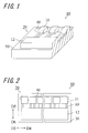
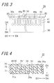
- the optical transmission module 10 shown in Figs. 1 and 2 includes the optical transmission structure 20, an optoelectronic conversion device 11 used as an optical device, and a circuit component 12.
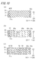
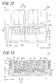
- the optical transmission structure 20 shown in Figs. 3 and 4 includes a main substrate 30, a cladding member 40, a plurality of core members 50, and an electric wiring 60.
- the main substrate 30 acts to support the cladding member 40, the core members 50, and the electric wiring 60.
- the thickness of the main substrate 30 may fall in the range of, for example, 0.1 mm or more and 2 mm or less.
- the main substrate 30 for example, use can be made of an epoxy resin substrate formed of a glass base material, a copper-clad substrate formed of a glass base material, a polyimide resin substrate, and a ceramic substrate.
- the main substrate 30 is constructed of a single-layer substrate or a stacked body made of a stack of a plurality of substrates. In this embodiment, a plurality of ceramic substrates are employed.
- the main substrate 30 of this embodiment is constructed by stacking a plurality of secondary substrates 31 together.
- the main substrate 30 has a through hole 30a penetrating therethrough in a thickness direction thereof.
- the through hole 30a is composed of a series of secondary through holes 31a disposed in the secondary substrates 31.
- the secondary through holes 31a are disposed in the respective secondary substrates 31 so as to penetrate therethrough in the thickness direction.
- said thickness direction is defined as "a D1-D2 direction”.
- the cladding member 40 In the interior of the through hole 31a is disposed the cladding member 40 in such a way as to fill the through hole 31a.
- the cladding member 40 acts to support the plurality of core members 50 disposed in the interior thereof.
- the cladding member 40 has a plurality of through holes penetrating therethrough in a thickness direction thereof. Said plurality of through holes are each defined as an optical waveguide hole 40a.
- the optical waveguide holes 40a are arranged along one direction which is perpendicular to the thickness direction. Said one direction is defined as a first direction in this embodiment. In Figs. 2 to 4 , the first direction is defined as "a D3-D4 direction". Moreover, the first direction corresponds to the direction of the plane of the main substrate 30.
- each of the optical waveguide holes 40a is disposed the core member 50. That is, the plurality of core members 50 are arranged along the first direction (the D3-D4 direction), and each of them is so formed as to extend in the thickness direction (the D1-D2 direction).
- the spacing between the core members 50 in the first direction may fall in the range of 62.5 ⁇ m or more and 250 ⁇ m or less.
- the diameter of the core member 50 along the first direction may fall in the range of 10 ⁇ m or more and 100 ⁇ m or less.
- the core member 50 functions as an optical waveguide 20a of the optical transmission structure 20.
- a refractive index of the core member 50 is greater than a refractive index of the cladding member 40.
- the core member 50 is able to serve as the optical waveguide 20a. That is, the cladding member 40 functions as a so-called cladding of the optical waveguide 20a, whereas the core member 50 functions as a core of the optical waveguide 20a.
- the refractive index of the core member 50 may be so determined that the relative refractive index difference between the core member 50 and the cladding member 40 falls in the range of 0.8% or more and 4% or less.
- the plurality of core members 50 are disposed in one through hole 30a, in contrast to a case where a single core member is disposed in one through hole, it is possible to reduce the center-to-center spacing between cores. That is, in the optical transmission structure 20 of this embodiment, only the cladding member 40 lies between two the optical waveguide holes 40a, wherefore the center-to-center spacing between cores can be reduced. Moreover, as practiced in this embodiment, the use of a multilayer ceramic substrate for the main substrate 30 makes it possible to increase the degree of tolerance for misregistration of the plurality of secondary substrates 31 in stacking operation.
- a variety of resin materials may be used for the formation of the cladding member 40, and examples thereof include epoxy resin, acrylic resin, and polyimide resin.
- a photosensitive resin is adopted as the material of formation of the cladding member 40. The use of a photosensitive resin makes it possible to form the optical waveguide hole 40a by means of photolithography.
- the first advantage resides in the effect of minimizing relative positional deviation between the plurality of optical waveguide holes 40a. This is because the plurality of optical waveguide holes 40a can be formed simultaneously by a single exposure process. Minimization of positional deviation in the optical waveguide holes 40a makes it possible to achieve, when establishing optical connection with other different optical waveguide placed in a location spaced outward from the optical transmission structure 20, successful transmission of light propagating through the interior of the optical waveguide hole 40a to said other optical waveguide.
- the degree of relative positional deviation between a plurality of optical waveguides is less than or equal to 5 ⁇ m.
- the positional deviation depends on positional deviation in masking portions of a photomask corresponding to the optical waveguide holes 40a.
- a manufacturing error for the photomask can be kept at a level of less than 1 ⁇ m, wherefore the degree of positional deviation in the optical waveguide holes 40a can be reduced to 5 ⁇ m or less.
- the second advantage resides in the effect of imparting smoothness to the inner wall of the optical waveguide hole 40a. This is because the optical waveguide hole 40a is formed by exploiting light which travels straightforward with high linearity. By rendering the inner wall surface of the optical waveguide hole 40a smooth, it is possible to lessen losses of light propagating through the interior of the optical waveguide hole 40a. As a knowledge among those skilled in the art, it is preferable that the roughness of the inner wall surface of the optical waveguide hole 40a is sufficiently low with respect to the wavelength of light propagating through the interior of the optical waveguide hole.
- the electric wiring 60 is electrically connected to the optoelectronic conversion device 11 optically coupled to the core member 50.
- the electric wiring 60 includes a surface wiring layer 61 disposed on a surface of the main substrate 30 on the D1 direction side.
- the electric wiring 60 may further include a through conductor configured to penetrate through the secondary substrate 31, as well as an intermediate wiring layer disposed between two secondary substrates 31.
- the through conductor may either be shaped so that it is hollowed in the middle or be shaped so that it is filled with an electrically conductive paste or the like in the middle.
- the through conductor can be formed by means of plating, metal-film vapor deposition, electrically conductive resin injection, or otherwise.
- the electric wiring 60 makes, at its surface wiring layer 61, electrical connection with the optoelectronic conversion device 11.
- the optoelectronic conversion device 11 of this embodiment is mounted on the surface wiring layer 61 of the electric wiring 60 by using a metal bump, an electrically conductive adhesive, or the like. Regions other than the juncture of the optoelectronic conversion device 11 and the surface wiring layer 61 may be covered with a protective layer.
- the optoelectronic conversion device 11 has the function of emitting light in response to inputted electric signals, or the function of effecting conversion into electric signals in response to incident light.
- the optoelectronic conversion device 11 is optically coupled to the optical waveguide 20a.
- the optoelectronic conversion device 11 of this embodiment performs the function of transmitting optical signals to the optical waveguide 20a in response to electric signals inputted thereto through the electric wiring 60, or the function of transmitting electric signals to the electric wiring 60 in response to optical signals inputted thereto through the optical waveguide 20a.
- the optoelectronic conversion device 11 for emitting light As described above, a variety of light-emitting devices are applicable. For example, a vertical cavity surface emitting laser (VCSEL) can be used for the optoelectronic conversion device 11.
- VCSEL vertical cavity surface emitting laser
- a variety of light-receiving devices, such as a photo diode (PD) are applicable. In the case of employing a PD as such a light-receiving device, it is desirable to use a fast-responsive device, for example, a PIN-PD.
- the optoelectronic conversion device 11 may either be constructed of one element provided with a single photoelectric conversion section or be constructed of one element provided with a plurality of photoelectric conversion sections.
- the optoelectronic conversion device 11 of this embodiment is constructed of one element provided with a single photoelectric conversion section.
- a single photoelectric conversion section is so disposed as to be brought into correspondence with a single core member 50.
- Said single photoelectric conversion section is so disposed as to be brought into correspondence with a single optical waveguide 20a.
- the circuit component 12 is electrically connected to the optoelectronic conversion device 11 through the electric wiring 60.
- the function of the circuit component 12 varies according to the function of the optoelectronic conversion device 11.
- the circuit component 12 effects inputting of a modulated electric signal (modulation voltage) to the optoelectronic conversion device 11 for control of the luminescence intensity of the optoelectronic conversion device 11.
- the circuit component 12 converts the output of a current signal produced responsive to the intensity of an optical signal received by the optoelectronic conversion device 11 into a voltage signal and produces the voltage signal output.
- the circuit component 12 may have the capability to control signal waveforms or the capability to remove noise components. In a case where electric-signal output from the optoelectronic conversion device 11 is small, it is advisable to impart signal amplification capability to the circuit component 12. This signal amplification capability may be possessed by the optoelectronic conversion device 11 in itself. Moreover, the circuit component 12 may also have the capability to perform logic operations and mathematical calculations.
- a main surface 20' of the optical transmission structure 20 may have the form of a flat surface.
- the main surface 20' of the optical transmission structure 20 it is possible to facilitate the mounting of the optical device optically coupled to the core member 50. That is, in this case, since the optical device can be mounted on the main surface 20' of the optical transmission structure 20 with ease, when establishing optical connection of the optical device to the optical transmission structure 20, it is possible to suppress an optical loss which is likely to occur between the optical device and the optical transmission structure 20.
- the optical waveguide hole 20a may be so shaped that the cross-sectional area of its section perpendicular to the thickness direction (the D1-D2 direction) becomes smaller gradually from one end (toward the main surface 20' of the optical transmission structure 20) to a point midway between said one end and the other end (toward a second main surface 20" of the optical transmission structure 20).
- the optical waveguide hole 20a is so shaped that the cross-sectional area becomes smaller gradually from one end to the other end, for example, the percentage of the cross-sectional area drops from 100% to 80%.
- the optical waveguide hole 20a may be formed with a taper portion 50' in which the cross-sectional area of its section perpendicular to the thickness direction (the D1-D2 direction) becomes smaller gradually from one end (toward the main surface 20' of the optical transmission structure 20) to the other end (toward the second main surface 20" of the optical transmission structure 20).
- the taper portion 50' obtained by tapering the optical waveguide hole from one end to a point midway between said one end and the other end, in the optical transmission structure 20 with the optical device mounted thereon, when light enters the core member 50 from said optical device, or when light enters the optical device from the core member 50, it is possible to lessen coupling losses.
- each of their confronting side surfaces 40a 1 may be shaped as a flat surface.
- the side surfaces 40a 1 of, respectively, the two adjacent optical waveguide holes 40a are each shaped as a flat surface, it is possible to arrange the optical waveguide holes 40a closer to each other. That is, the two adjacent optical waveguide holes 40a can be arranged at as close a spacing as possible.
- the flat surfaces constituting the confronting side surfaces 40a 1 of the two optical waveguide holes 40a arranged adjacent each other in the first direction may be increased in size in a second direction (the D5-D6 direction).
- the optical waveguide hole 40a is elongated in the second direction intersected by the first direction.
- optical waveguide hole 40a its section taken along the planar direction of the main substrate 30 has a non-circular shape, or more specifically nearly the shape of a rounded rectangle. That is, strictly speaking, the "rounded rectangle" is a figure defined by two equal-length parallel lines and two semicircles, but, in this embodiment, the sectional profile is not limited to such a precise rounded rectangle.
- the optical waveguide hole 40a constitutes a through hole defined by two side surfaces 40a 1 connected to each other by two curved surfaces 40a 2 .
- Fig. 8 As another shape of the section of the optical waveguide hole 40a taken along the planar direction, for example, as shown in Fig. 8 , polygonal shapes including a rectangular shape, a hexagonal shape, and an octagonal shape can be employed.
- Fig. 8(a) shows a rectangular-shaped optical waveguide hole 40j
- Fig. 8(b) shows a hexagonal-shaped optical waveguide hole 40k
- Fig. 8(c) shows a trapezoidal-shaped optical waveguide hole 401.
- the side surface of each optical waveguide hole is designated by the corresponding reference symbol with a numerical subscript of 1.
- each second through hole 40a In the interior of each second through hole 40a is disposed the core member 50.
- the core member 50 is so shaped as to conform to the shape of the optical waveguide hole 40a. That is, a plurality of core members 50 are arranged along the first direction, and each of them is so formed as to extend in the thickness direction.
- the spacing between the core members 50 in the first direction may fall in the range of 62.5 ⁇ m or more and 250 ⁇ m or less.
- the diameter of the core member 50 along the first direction may fall in the range of 10 ⁇ m or more and 100 ⁇ m or less.
- their confronting side surfaces 50a extend along the second direction.
- its section taken along the planar direction of the main substrate 30 has a non-circular shape, or more specifically nearly the shape of a rounded rectangle.
- Fig. 8(a) shows a rectangular-shaped core member 50j
- Fig. 8(b) shows a hexagonal-shaped core member 50k
- Fig. 8(c) shows a trapezoidal-shaped core member 501.
- the side surface of each core member is designated by the corresponding reference symbol with a numerical subscript of 1.
- the optical waveguide hole 40a can be given a desired shape, and this is an advantage which accrues from the use of photolithography for the boring of the optical waveguide hole 40a.
- the conventional art in the course of forming an optical waveguide hole, since an optical through hole is created by means of drilling, it is difficult to shape the hole into a figure other than a true circle, wherefore the shape of the through hole is practically limited to a true circle. Even if the hole can be shaped into a figure other than a true circle, much time needs to be spent in the shaping operation, which leads to poor shaping reproducibility.
- the diameter of the optical waveguide hole 40a may fall in the range of 10 ⁇ m or more and 100 ⁇ m or less, and it will thus be difficult to prepare a cutting edge of a size smaller than the diameter in this range. Even if a cutting edge of such a diameter can be prepared, the cutting edge is so brittle that it is hard to perform cutting work.
- the main substrate 30 of this embodiment is produced by performing the following steps. At first, as shown in Fig. 9(a) , a plurality of green sheets 31X that are formed into secondary substrates 31 by firing process are prepared. Next, as shown in Fig. 9(b) , a sheet hole 31Xa is formed in the green sheet 31X to provide a secondary through hole 31a. Concurrently with the formation of the sheet hole 31Xa, a through hole used for a through conductor of an electric wiring 60 is formed on an as needed basis. Such holes can be made by various methods, for example, by punching out the sheet with a pin or die or by cutting the sheet with laser light. Next, a metal paste for forming the electric wiring 60 is placed on the green sheet 31X.
- the metal paste can be prepared by utilizing screen printing technique or ink-jet printing technique, for example.
- a paste containing metal such as tungsten (W), molybdenum (Mo), manganese (Mn), silver (Ag), and copper (Cu) can be used.
- the green sheets 31X are stacked on top of each other so that the sheet holes 31Xa can be continuous with each other.
- the stacked green sheets 31X are fired, thereby constituting the main substrate 30 formed with the through hole 30a as shown in Fig. 9(d) . Concurrently with the firing of the green sheets 31X, the metal paste is fired to constitute the electric wiring 60.
- the through hole 30a of the main substrate 30 is filled with a photosensitive material 40X that can be formed into a cladding member 40 by curing process.
- the photosensitive material include an epoxy resin-based material, an acrylic resin-based material, and a polyimide resin-based material.
- a negative photoresist whose solubility in a developer solution is decreased through exposure to light.
- the pre-baked photosensitive material 40X is exposed to light.
- the exposure process is performed with use of a light-transmitting plate such as a photomask having a plurality of light-shielding portions for blocking light to avoid application of light to a region for forming an optical waveguide hole 40a.
- a photomask By means of such a photomask, in the pre-baked photosensitive material 40X, its region other than the region in overlapping relation with the above-described light-shielding portion is exposed to light.
- the exposed photosensitive material 40X is heated (post-baked). Then, the post-baked photosensitive material 40X is developed by a developer solution so that the exposed part of the photosensitive material 40X can be turned into the cladding member 40, whereupon, as shown in Fig. 10(b) , the cladding member 40 having the optical waveguide hole 40a is formed.
- a light-transmiting material for forming a core member 50 is filled into the optical waveguide hole 40a of the cladding member 40. After that, the filled light-transmitting material is cured by means of application of light having a predetermined wavelength, baking, or otherwise, thereby forming the core member 50 as shown in Fig. 10(c) .
- the light-transmitting material for forming the core member 50 in the optical waveguide hole 40a it is advisable to polish the main surface 20' of the optical transmission structure 20 for planarization.
- the light-transmitting material for forming the core member extends off the main surface 20' of the optical transmission structure 20, by planarizing the main surface 20' of the optical transmission structure 20, it is possible to facilitate mounting of an optical device and so forth thereon.
- chemical mechanical polishing technique can be adopted as the method of polishing the main surface 20' of the optical transmission structure 20.
- optical transmission module 10A which exemplifies the optical transmission module of the invention by way of a second embodiment will be described with reference to the drawings.
- the optical transmission module 10A shown in Fig. 11 includes an optical transmission structure 20A, an optoelectronic conversion device 11 used as an optical device, and a circuit component 12.
- the optoelectronic conversion device 11, as well as the circuit component 12, is structurally similar to that as particularized hereinabove, and the description thereof will therefore be omitted.
- the optical transmission structure 20A shown in Figs. 11 and 12 differs structurally from the optical transmission structure 20 in that a main substrate 30A is adopted instead of the main substrate 30 and that an optical wiring substrate 21 is provided. Other portions of the optical transmission structure 20A are structurally identical to those of the optical transmission structure 20, and overlapping descriptions will thus be omitted.
- the main substrate 30A differs structurally from the main substrate 30 in that a bearing hole 30Ab is formed. Other portions of the optical transmission structure 20A are structurally identical to those of the optical transmission structure 20, and overlapping descriptions will thus be omitted.
- the bearing hole 30Ab serves as the reference for optical alignment of the optical waveguide 20a.
- the bearing hole 30Ab is formed by recessing the main substrate 30A in a direction from, of both main surfaces thereof, one main surface 20' on the D1 direction side toward the D2 direction. That is, the bearing hole 30Ab is opened at the main surface 20" opposite from the main surface which bears the optoelectronic conversion device 11.
- the bearing hole 30Ab of this embodiment passes completely through the substrate in the thickness direction thereof. Note that the bearing hole 30Ab is not limited to a hole penetrating in the thickness direction (the D1-D2 direction).
- the core member 50 is placed between these bearing holes 30Ab.
- the two bearing holes 30Ab and an array of a plurality of core members 50 are arranged along the first direction (the D3-D4 direction).
- the centers of the bearing holes 30Ab and the centers of the core members 50 are arranged along the first direction.
- the proper arrangement of the bearing holes 30Ab and the core members 50 can be made with ease by using the bearing holes 30Ab as the reference in the process of exposing the region for forming the optical waveguide hole 40a to light.
- the bearing holes 30Ab and the core members 50 in one direction and also locating the bearing hole 30Ab at each end of the array of the core members 50, it is possible to control surface inclination with respect to other optical wiring components as will hereafter be described (for example, an optical transmission layer 80, an optical path changing portion 82b).
- the optical wiring substrate 21 includes a support substrate 70, the optical transmission layer 80, and an optical axis member 90. While the optical wiring substrate 21 of this embodiment includes the optical axis member 90, the optical axis member 90 does not necessarily have to be provided.
- the support substrate 70 acts to support other constituents of the optical wiring substrate 21. Moreover, the support substrate 70 may have the function of providing electrical connection between the optical transmission structure 20A and other electric elements.
- a build-up substrate which is composed of a base body and a build-up layer and has a through conductor, is preferably used.
- the build-up layer is composed of a resin insulating layer and an electrically conductive layer. For example, thermosetting epoxy resin, bismaleimide triazine resin, or the like is used for the resin insulating layer.
- the thickness of the resin insulating layer may fall in the range of, for example, 10 ⁇ m or more and 70 ⁇ m or less. It is preferable that the resin insulating layer is capable of being subjected to laser micromachining for pore formation. By virtue of the resin insulating layer, it is possible to stack the build-up layers together while effecting routing of complicated electric wiring patterns and integration in a narrow range.
- the support substrate 70 has a bearing hole 70a formed by recessing the support substrate in the direction from one main surface on the D1 direction side toward the D2 direction.
- the bearing hole 70a is situated so as to pair up with the bearing hole 30Ab of the main substrate 30.
- the bearing hole 70a serves as the reference for optical alignment between the optical transmission layer 80 and the core member 50.
- the optical transmission layer 80 includes an optical transmission cladding member 81 and an optical transmission core member 82.
- the optical transmission cladding member 81 functions as the base body of the optical transmission layer 80.
- the optical transmission core member 82 is formed inside the optical transmission cladding member 81.
- a refractive index of the optical transmission core member 82 is greater than a refractive index of the optical transmission cladding member 81. So long as the refractive index of the optical transmission core member 82 is greater than that of the optical transmission cladding member 81, the optical transmission layer 80 is capable of confinement of optical signals and is thus able to serve as an optical waveguide.
- the optical transmission core member 82 of this embodiment is so designed that a part thereof functions as an optical waveguide 82a.
- the refractive index of the optical transmission core member 82 is preferably so determined that the relative refractive index difference between the optical transmission core member 82 and the optical transmission cladding member 81 falls in the range of 0.8% or more and 4% or less.
- a plurality of optical transmission core members 82 are formed inside the optical transmission cladding member 81, and each of them extends along a certain extending direction.
- the extending direction is defined as "the D5-D6 direction”.
- the plurality of optical transmission core members 82 are arranged along the above-described first direction.
- the extending direction in which the optical transmission core member 82 extends is equivalent to the direction of optical transmission.
- the dimension of the optical transmission core member 82 in the direction of the plane along the first direction and the thickness direction, or the planar direction D1, D2-D3, D4, the length of one side or the diameter of the optical transmission core member 82 may advisably fall in the range of 10 ⁇ m or more and 100 ⁇ m or less.
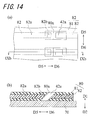
- the optical transmission core member 82 is formed with the optical path changing portion 82b.
- the optical path changing portion 82b is formed at an end of the optical waveguide 82a as shown in in Fig. 14(a) .
- the optical path changing portion 82b has the capability of enabling a change in an optical path so that light propagating through the optical waveguide 82a can be directed to outside of the optical waveguide 82a, or the capability of enabling a change in an optical path so that incoming light from outside of the optical waveguide 82a can be directed to the interior of the optical waveguide 82a.
- optical waveguide 82a that part thereof which is located on the D5 direction side relative to the optical path changing portion 82b in the extending direction serves as the optical waveguide 82a, whereas that part thereof which is located on the D6 direction side relative to the optical path changing portion 82b in the extending direction does not serve as the optical waveguide 82a.
- a light-reflecting face is formed as the optical path changing portion 82b.
- the light-reflecting face is inclined with respect to the optical axis of the optical waveguide 82a, and enables a change in an optical path by reflection of light.
- As the angle of inclination of the light-reflecting face it is possible to use an angle obtained by bisecting the angle which the direction of the optical axis of the optical waveguide 82a forms with the direction of a redefined optical path, and, for example, the light-reflecting face is formed at an inclination angle which falls in the range of the bisected angle ⁇ 3 degrees.
- the optical transmission layer 80 of this embodiment has a cavity 42a formed by recessing the top surface thereof.
- the optical transmission cladding member 81 and the optical transmission core member 82 are left exposed at the inner periphery thereof.
- a single optical transmission core member 82 is divided into two segments by the cavity 42a.
- part of the optical transmission core member 82 left exposed at the inner surface of the cavity 42a serves as a light-reflecting face.
- this light-reflecting face constitutes the optical path changing portion 82b.
- the upper surface of the optical path changing portion 82b may be covered with a reflective film such as a metal film.
- the cavity 42a serves as an entrance opening for admitting light into the optical waveguide 82a via the light-reflecting face, or an exit opening for taking out light propagating through the optical waveguide 82a via the light-reflecting face.
- the light-reflecting face is inclined at an angle of about 45°, or more specifically an angle in the range of 42 to 48°, with respect to the extending direction and the thickness direction.
- the cavity 42a may either be shaped as a hollow or be filled with some material in so far as it is able to serve as the entrance or exit opening.
- Exemplary of the material of formation of the optical transmission cladding member 81 and the optical transmission core member 82 is a resin capable of being subjected to direct exposure process or a resin capable of being subjected to refractive-index variation process.
- the resin capable of being subjected to direct exposure process include a photosensitive resin such as epoxy resin, acrylic resin, and polyimide resin.
- examples of the resin capable of being subjected to refractive-index variation process include a resin whose refractive index is decreased by Ultra-Violet (UV) radiation, such as polysilane.
- the direct exposure process is a method for forming the optical transmission layer 80 by forming the lower part of the optical transmission cladding member 81, followed by forming the optical transmission core member 82 thereon by coating the material of formation of the optical transmission core member 82 and exposing it to light with masks, and further coating the material of formation of the optical transmission cladding member 81 on the top and side surfaces of the optical transmission core member 82.
- the refractive-index variation process is a method for forming the optical waveguide by performing UV radiation on a region other than the region for forming the optical transmission core member 82 to reduce the refractive index of the region other than the region for forming the optical transmission core member 82.
- the optical axis member 90 is an axis member which serves as the reference for optical alignment of the optical waveguide 20a and the optical waveguide 82a.
- the optical axis member 90 is inserted in the bearing hole 30Ab as well as in the bearing hole 70a.
- a member in the form of a straight rod can be used for the optical axis member 90.
- the shape of the core member 50 of the modified example 4 of the first embodiment of the optical transmission structure as described above may be applied to the optical transmission structure 20A and the optical transmission module 10A of this embodiment.
- the core member 50 of the optical transmission structure 20A may be given a polygonal sectional profile.
- the optical transmission core member 82 of the optical transmission layer 80 and the core member 50 are identical in shape, it is possible to suppress an optical loss that occurs when light which exited from the core member 50 enters the optical transmission layer 80.
- the core member 50 is so shaped that, when viewed in a plan view, as compared to its transverse width parallel to the first direction (the D3-D4 direction), its longitudinal width parallel to the second direction (the D5-D6 direction) intersected by the first direction is larger, it is possible to dispose the optical transmission layer 80 in a direction parallel to the second direction.
- the optical transmission layer 80 By disposing the optical transmission layer 80 as such, an optical signal can be transmitted through the optical waveguide 80a and reflected from the optical path changing portion 82b while being restrained from light diffusion in a direction intersected by the transmission direction.
- the construction of this embodiment it is possible to increase virtually the area of the opening for the optical waveguide 80a while reducing the spacing between the optical waveguide holes 40a. Accordingly, the construction of this embodiment is capable of both miniaturization and suppression of losses entailed by optical coupling between the optical waveguide 20a and the optical waveguide 80a.
- a second cladding member 23 is disposed between a cladding member 22 and a core member 24. More specifically, the second cladding member 23 is situated between the cladding member 22 and the core member 24 so as to surround the core member 24. Moreover, a refractive index of the second cladding member 23 is smaller than a refractive index of the core member 24.
- the diameter of the core member 24 can be reduced.
- the term "diameter” refers to the diameter of the section taken along the planar direction.
- the reduction of the diameter of the core member 24 affords the following advantages. In the case of mounting a light-emitting device as an optoelectronic conversion device 30 on the optical transmission board 20B, when the optical waveguide 20a is optically coupled to other different optical waveguide, it is possible to lessen losses entailed by a misalignment in optical axis between these optical waveguides.
- a light-receiving device having a small light-receiving section can be adopted.
- a photodiode has a negative correlation between the size of a light-receiving section and the speed of response, and in fact, the smaller the light-receiving section is, the faster the response is. That is, in the case of mounting a light-receiving device on the optical transmission board 20B, speeding-up of the response can be achieved.
- a material which is smaller in refractive index than the cladding member 22 can be used for the second cladding member 23.
- the relative refractive index difference between the second cladding member and the core member 24 which serves as the optical waveguide 20a can be increased with ease. That is, the use of a material having a relatively small refractive index for the second cladding member 23 makes it possible to extend the range of material choices for the core member 24.
- a method for manufacturing the optical transmission structure 2B that exemplifies the method of manufacturing the optical transmission structure in accordance with the third embodiment will be described with reference to the drawings.
- a substrate as shown in Fig. 17(a) which is composed of a stack of a plurality of secondary substrates 211 and a cladding member 22 with an optical waveguide hole 22a set in a through hole 21a, is prepared by using the method for manufacturing the optical transmission structure in accordance with the first embodiment as described above.
- a precursor of a resin material in liquid form for forming the second cladding member 23 is applied to the inner wall of the optical waveguide hole 22a of the cladding member 22. It is advisable to exploit negative pressure for the application of the resin material precursor. Specifically, at first, pressure adjustment is made so that, as compared to the atmospheric pressure at one side of the opening of a first optical waveguide hole 22a, the atmospheric pressure at the other side becomes lower. Next, the resin material precursor in liquid form is poured from said one side. The resin material precursor is drawn into the opening under the difference in atmospheric pressure so as to be applied to the inner wall of the first optical waveguide hole 22a, and a through hole for the passage of air is formed in the middle. This through hole serves as the first optical waveguide hole 22a. Lastly, the resin material precursor is cured, thereby forming the second cladding member 23.
- a light-transmitting material for forming the core member 24 is filled into a second optical waveguide hole 23a of the second cladding member 23. Subsequently the light-transmitting material is cured, thereby forming the core member 24 as shown in Fig. 17(c) .
- the optical transmission board 20B shown in Figs. 15 and 16 is produced.
- the optical transmission structure 20C shown in Fig. 18 differs structurally from the optical transmission structure 20 in that a main substrate 30C is adopted instead of the main substrate 30 and that a cladding member 40B is adopted instead of the cladding member 40.
- Other portions of the optical transmission structure 20C are structurally identical to those of the optical transmission structure 20, and overlapping descriptions will thus be omitted.
- the optical transmission structure 20C includes a substrate 30B having a plurality of through holes 30Ba penetrating therethrough in a thickness direction (the D1-D2 direction) thereof; a cladding member 40B having an optical waveguide hole 40Ba penetrating therethrough in a thickness direction thereof and disposed in at least one of the plurality of through holes 30Ba; and a plurality of core members 50B disposed inside the optical waveguide hole 40B, respectively, which are greater in refractive index than the cladding member 40B.
- the main substrate 30C has a plurality of through holes 30Ba.
- the plurality of through holes 30Ba are arranged in the first direction (the D3-D4 direction).
- Each of the plurality of through holes 30Ba is provided with the cladding member 40B.
- the cladding member 40B is provided with at least one optical waveguide hole 40Ba.
- the optical waveguide holes 40Ba are arranged along the first direction.
- Each of the plurality of optical waveguide holes 40Ba is provided with a single core member 50B.
- the through holes 30Ba do not necessarily have to be arranged in a row along the first direction, and also the plurality of through holes 30Ba do not necessarily have to be equi-spaced in the first direction.
- the optical waveguide holes 40Ba are arranged linearly along the first direction, and are also nearly equi-spaced.
- optical transmission structure 20B of this embodiment are structurally identical to those of the optical transmission structure 20, and overlapping descriptions will thus be omitted. Note that, although the optical transmission structure 20B of this embodiment does not employ the bearing hole 30Ab and the optical wiring substrate 21 adopted in the optical transmission structure 20A, these components may be adopted in this embodiment.
- the production of such an optical transmission structure 20C can be based mainly on the method for manufacturing the optical transmission structure 20 in accordance with the first embodiment described above. Differences from the method for manufacturing the optical transmission structure 20 include forming the plurality of through holes 30Ba in the substrate 30B and providing the optical waveguide hole 40Ba in the through hole 30Ba. In this way, since the cladding member 40B bearing the optical waveguide hole 40B is formed by means of photolithography, it is possible to impart smoothness to the inner wall of the optical waveguide hole 40B, and thereby lessen losses of light propagating through the core member 50B disposed in the interior of the optical waveguide hole 40a. Also in the case of forming the optical waveguide hole 40Ba in the cladding member 40B placed inside the through hole 30B, the formation can be accomplished with ease by virtue of simultaneous exposure process.
- the optical transmission structure 20D shown in Fig. 19 differs structurally from the optical transmission structure 20 in that a main substrate 30D is adopted instead of the main substrate 30 and that a cladding member 40D is adopted instead of the cladding member 40.
- Other portions of the optical transmission structure 20C are structurally identical to those of the optical transmission structure 20, and overlapping descriptions will thus be omitted.
- the main substrate 30D has a plurality of through holes 30Ca.
- the plurality of through holes 30Ca are arranged in the first direction (the D3-D4 direction).
- Each of the plurality of through holes 30Ca is provided with the cladding member 40C.
- Each of the cladding member 40C is provided with a plurality of optical waveguide holes 40Ca. While, in the optical transmission structure 20C shown in Fig. 19 , two optical waveguide holes 40Ca are provided in a single cladding member 40C, the number of the optical waveguide holes is not so limited, and therefore three or more optical waveguide holes may be provided.
- the plurality of optical waveguide holes 40Ca are arranged along the first direction. Each of the plurality of optical waveguide holes 40Ca is provided with a single core member 50C.
- the plurality of through holes 30Ca do not necessarily have to be arranged in a row along the first direction, and also the plurality of through holes 30Ca do not necessarily have to be equi-spaced in the first direction.
- the optical waveguide holes 40Ca are arranged linearly along the first direction, and are also nearly equi-spaced.
- optical transmission structure 20C of this embodiment are structurally identical to those of the optical transmission structure 20, and overlapping descriptions will thus be omitted. Note that, although the optical transmission structure 20C of this embodiment does not employ the bearing hole 30Ab and the optical wiring substrate 21 adopted in the optical transmission structure 20A, these components may be adopted in this embodiment.
- optical transmission structure 20D can be based mainly on the method for manufacturing the optical transmission structure 20 in accordance with the first embodiment described above. Differences from the method for manufacturing the optical transmission structure 20 include forming the plurality of through holes 30Ba in the substrate 30B and providing the plurality of optical waveguide holes 40Ba in the through hole 30Ba.
- the cladding member 40B bearing the plurality of optical waveguide holes 40B is formed by means of photolithography, it is possible to form the cladding members 40B each bearing the plurality of optical waveguide holes 40B at the same time, and also, in contrast to the case of forming the optical waveguide holes by conventional cutting technique, it is possible to shorten the time required for the process to form the optical waveguide holes 40B, as well as to facilitate control of the positions of the optical waveguide holes 40B and control of the shape of the inner wall thereof.
- the method for manufacturing the optical transmission structure 20 as described hereinabove is directed to the adoption of a ceramic substrate for the main substrate 30, it is possible to produce the optical transmission structure with use of an organic substrate.
- the resultant base body is subjected to punching operation to form through holes in the substrates.
- positional deviation between secondary through holes can be minimized.
- the optical transmission layer 80 does not necessarily have to be supported.
- the cladding member 40 and the core member 50 may be optically connected to the optical transmission layer 80 via a connector.
Landscapes
- Physics & Mathematics (AREA)
- General Physics & Mathematics (AREA)
- Optics & Photonics (AREA)
- Engineering & Computer Science (AREA)
- Microelectronics & Electronic Packaging (AREA)
- Optical Integrated Circuits (AREA)
Abstract
Description
- The present invention relates to an optical transmission structure and a method for manufacturing the same, and an optical transmission module.
- Recently, in the interest of enhancement in information processing capacity, researches and studies have been conducted as to replacement with an optical transmission system in regard to telecommunication between electrical devices such as integrated circuit components. For example, in
Patent Literature 1, there is disclosed an optical transmission module constructed by mounting a plurality of optoelectronic conversion devices such as light-emitting devices in an optical transmission structure having a plurality of optical waveguides extending in the direction of substrate thickness. The optical waveguides are disposed in a plurality of through holes, respectively, formed so as to pass completely through the substrate in its thickness direction. -
- Patent literature 1: Japanese Unexamined Patent Publication
JP-A 2004-294857 - However, in the optical transmission structure disclosed in
Patent literature 1, in light of dimensional deviation or positioning error such as misalignment that occurs during the forming of the through holes, and substrate strength as well, restrictions need to be imposed on the diameter, position, etc. of the optical waveguide. - The present invention has been devised in view of the circumstances as mentioned supra, and accordingly an object of the invention is to provide an optical transmission structure having a high degree of flexibility in the design of an optical waveguide and a method for manufacturing the optical transmission structure, and also an optical transmission module.
- An optical transmission structure in accordance with a first embodiment of the invention includes: a substrate having a through hole penetrating therethrough in a thickness direction thereof; a cladding member which is disposed inside the through hole and has a plurality of optical waveguide holes penetrating therethrough in a thickness direction thereof; and a plurality of core members disposed in inside the plurality of optical waveguide holes, respectively.
- An optical transmission module in accordance with an embodiment of the invention includes: the optical transmission structure mentioned above; and an optical device optically coupled to the second optical member.
- An optical transmission structure in accordance with a second embodiment of the invention includes: a substrate having a plurality of through holes penetrating therethrough in a thickness direction thereof; a cladding member having an optical waveguide hole penetrating therethrough in the thickness direction and disposed inside at least one of the plurality of through holes; and a plurality of core members which are disposed inside the optical waveguide hole, and have a refractive index larger than the cladding member.
- A method for manufacturing an optical transmission structure in accordance with the first embodiment of the invention includes: preparing a substrate having a through hole penetrating therethrough in a thickness direction thereof; filling a photosensitive material into the through hole; exposing a region of the photosensitive material filled other than a region thereof in overlapping relation with a plurality of light-shielding portions to light through a light-transmitting plate having the plurality of light-shielding portions for photosensitization, and then turning the photosensitized photosensitive material into a cladding member; forming a plurality of optical waveguide holes penetrating in the thickness direction in the cladding member by removing the region of the photosensitive material in overlapping relation with the light-shielding portion; and filling a core member made of a light-transmitting material which has a refractive index larger than the cladding member into the optical waveguide hole.
- A method for manufacturing an optical transmission structure in accordance with the second embodiment of the invention includes: preparing a substrate having a plurality of through holes penetrating therethrough in a thickness direction thereof; filling a photosensitive material into at least one of the plurality of through holes; exposing a region of the photosensitive material filled other than a region thereof in overlapping relation with the light-shielding portion to light through a light-transmitting plate having a plurality of light-shielding portions for photosensitization, and then turning the photosensitized photosensitive material into a cladding member; forming a plurality of optical waveguide holes penetrating the photosensitive material in the thickness direction in the cladding member by removing the region of the photosensitive material in overlapping relation with the light-shielding portion; and filling a core member made of a light-transmitting material which has a refractive index larger than the cladding member into the optical waveguide hole.
- According to the invention, there are provided an optical transmission structure and an optical transmission module having an optical waveguide designed with higher dimensional accuracy and higher positional accuracy.
-
-
Fig. 1 is a partial perspective view showing the general constitution of a first embodiment of an optical transmission module pursuant to the invention; -
Fig. 2 is a plan view showing the general constitution of the optical transmission module shown inFig. 1 ; -
Fig. 3 is a plan view showing the general constitution of a first embodiment of an optical transmission structure constituting the optical transmission module shown inFig. 1 ; -
Fig. 4 is a sectional view taken along the line III-III shown inFig. 2 ; -
Fig. 5 is a sectional view of a modified example of the first embodiment of the optical transmission structure shown inFig. 3 , illustrating the section taken along the line III-III ofFig. 2 ; -
Fig. 6 is a sectional view of a modified example of the first embodiment of the optical transmission structure shown inFig. 3 , illustrating the section taken along the line III-III ofFig. 2 ; -
Fig. 7 is a plan view showing a modified example of the first embodiment of the optical transmission structure shown inFig. 3 ; -
Fig. 8 is a plan view showing part of a modified example of the first embodiment of the optical transmission structure shown inFig. 7 ; -
Fig. 9 is a main-part sectional view showing an example of a procedure for manufacturing the optical transmission structure shown inFig. 4 ; -
Fig. 10 is a main-part sectional view showing the subsequent steps of the procedure for manufacturing the optical transmission structure shown inFig. 9 ; -
Fig. 11 is a plan view showing the general constitution of a second embodiment of an optical transmission module pursuant to the invention; -
Fig. 12 is a plan view, with parts omitted, of the optical transmission module shown inFig. 11 ; -
Fig. 13 is a main-part sectional view taken along the line VIII-VIII shown inFig. 12 ; -
Fig. 14(a) is an enlarged plan view of the main part of an optical wiring substrate provided in the optical transmission module shown inFig. 11 , andFig. 14(b) is a main-part sectional view taken along the line IXb-IXb shown inFig. 14(a) ; -
Fig. 15 is a plan view showing the general constitution of a third embodiment of an optical transmission structure pursuant to the invention; -
Fig. 16 is a sectional view taken along the line II-II shown inFig. 15 ; -
Fig. 17 is a main-part sectional view showing an example of a procedure for manufacturing the optical transmission structure shown inFig. 15 ; -
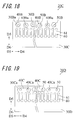
Fig. 18 is a plan view showing the general constitution of a fourth embodiment of an optical transmission structure pursuant to the invention; and -
Fig. 19 is a plan view showing the general constitution of a fifth embodiment of the optical transmission structure pursuant to the invention. - Hereinafter, an
optical transmission structure 20 and anoptical transmission module 10 that exemplify an optical transmission structure and an optical transmission module, respectively, according to a first embodiment of the invention will be described with reference to the drawings. - The
optical transmission module 10 shown inFigs. 1 and 2 includes theoptical transmission structure 20, anoptoelectronic conversion device 11 used as an optical device, and acircuit component 12. - The
optical transmission structure 20 shown inFigs. 3 and 4 includes amain substrate 30, acladding member 40, a plurality ofcore members 50, and anelectric wiring 60. - The
main substrate 30 acts to support thecladding member 40, thecore members 50, and theelectric wiring 60. For example, the thickness of themain substrate 30 may fall in the range of, for example, 0.1 mm or more and 2 mm or less. As themain substrate 30, for example, use can be made of an epoxy resin substrate formed of a glass base material, a copper-clad substrate formed of a glass base material, a polyimide resin substrate, and a ceramic substrate. Themain substrate 30 is constructed of a single-layer substrate or a stacked body made of a stack of a plurality of substrates. In this embodiment, a plurality of ceramic substrates are employed. Themain substrate 30 of this embodiment is constructed by stacking a plurality ofsecondary substrates 31 together. - As shown in
Fig. 4 , themain substrate 30 has a throughhole 30a penetrating therethrough in a thickness direction thereof. The throughhole 30a is composed of a series of secondary throughholes 31a disposed in thesecondary substrates 31. The secondary throughholes 31a are disposed in the respectivesecondary substrates 31 so as to penetrate therethrough in the thickness direction. InFig. 4 , said thickness direction is defined as "a D1-D2 direction". In the interior of thethrough hole 31a is disposed thecladding member 40 in such a way as to fill the throughhole 31a. - The
cladding member 40 acts to support the plurality ofcore members 50 disposed in the interior thereof. Thecladding member 40 has a plurality of through holes penetrating therethrough in a thickness direction thereof. Said plurality of through holes are each defined as anoptical waveguide hole 40a. Theoptical waveguide holes 40a are arranged along one direction which is perpendicular to the thickness direction. Said one direction is defined as a first direction in this embodiment. InFigs. 2 to 4 , the first direction is defined as "a D3-D4 direction". Moreover, the first direction corresponds to the direction of the plane of themain substrate 30. - In each of the
optical waveguide holes 40a is disposed thecore member 50. That is, the plurality ofcore members 50 are arranged along the first direction (the D3-D4 direction), and each of them is so formed as to extend in the thickness direction (the D1-D2 direction). For example, the spacing between thecore members 50 in the first direction may fall in the range of 62.5 µm or more and 250 µm or less. Moreover, for example, the diameter of thecore member 50 along the first direction may fall in the range of 10 µm or more and 100 µm or less. - The
core member 50 functions as anoptical waveguide 20a of theoptical transmission structure 20. A refractive index of thecore member 50 is greater than a refractive index of thecladding member 40. In this way, so long as the refractive index of thecore member 50 is greater than that of thecladding member 40, thecore member 50 is able to serve as theoptical waveguide 20a. That is, the claddingmember 40 functions as a so-called cladding of theoptical waveguide 20a, whereas thecore member 50 functions as a core of theoptical waveguide 20a. For example, the refractive index of thecore member 50 may be so determined that the relative refractive index difference between thecore member 50 and thecladding member 40 falls in the range of 0.8% or more and 4% or less. - In this construction, since the plurality of
core members 50 are disposed in one throughhole 30a, in contrast to a case where a single core member is disposed in one through hole, it is possible to reduce the center-to-center spacing between cores. That is, in theoptical transmission structure 20 of this embodiment, only thecladding member 40 lies between two theoptical waveguide holes 40a, wherefore the center-to-center spacing between cores can be reduced. Moreover, as practiced in this embodiment, the use of a multilayer ceramic substrate for themain substrate 30 makes it possible to increase the degree of tolerance for misregistration of the plurality ofsecondary substrates 31 in stacking operation. - A variety of resin materials may be used for the formation of the
cladding member 40, and examples thereof include epoxy resin, acrylic resin, and polyimide resin. In this embodiment, a photosensitive resin is adopted as the material of formation of thecladding member 40. The use of a photosensitive resin makes it possible to form theoptical waveguide hole 40a by means of photolithography. - In the case of forming the
optical waveguide hole 40a by means of photolithography, for example, the following advantages are gained. The first advantage resides in the effect of minimizing relative positional deviation between the plurality ofoptical waveguide holes 40a. This is because the plurality ofoptical waveguide holes 40a can be formed simultaneously by a single exposure process. Minimization of positional deviation in theoptical waveguide holes 40a makes it possible to achieve, when establishing optical connection with other different optical waveguide placed in a location spaced outward from theoptical transmission structure 20, successful transmission of light propagating through the interior of theoptical waveguide hole 40a to said other optical waveguide. - As a knowledge among those skilled in the art, it is preferable that the degree of relative positional deviation between a plurality of optical waveguides is less than or equal to 5 µm. In the case of employing the technique of photolithography, the positional deviation depends on positional deviation in masking portions of a photomask corresponding to the
optical waveguide holes 40a. In general, a manufacturing error for the photomask can be kept at a level of less than 1 µm, wherefore the degree of positional deviation in theoptical waveguide holes 40a can be reduced to 5 µm or less. - The second advantage resides in the effect of imparting smoothness to the inner wall of the
optical waveguide hole 40a. This is because theoptical waveguide hole 40a is formed by exploiting light which travels straightforward with high linearity. By rendering the inner wall surface of theoptical waveguide hole 40a smooth, it is possible to lessen losses of light propagating through the interior of theoptical waveguide hole 40a. As a knowledge among those skilled in the art, it is preferable that the roughness of the inner wall surface of theoptical waveguide hole 40a is sufficiently low with respect to the wavelength of light propagating through the interior of the optical waveguide hole. - The
electric wiring 60 is electrically connected to theoptoelectronic conversion device 11 optically coupled to thecore member 50. Theelectric wiring 60 includes asurface wiring layer 61 disposed on a surface of themain substrate 30 on the D1 direction side. Theelectric wiring 60 may further include a through conductor configured to penetrate through thesecondary substrate 31, as well as an intermediate wiring layer disposed between twosecondary substrates 31. The through conductor may either be shaped so that it is hollowed in the middle or be shaped so that it is filled with an electrically conductive paste or the like in the middle. The through conductor can be formed by means of plating, metal-film vapor deposition, electrically conductive resin injection, or otherwise. - As described above, the
electric wiring 60 makes, at itssurface wiring layer 61, electrical connection with theoptoelectronic conversion device 11. Theoptoelectronic conversion device 11 of this embodiment is mounted on thesurface wiring layer 61 of theelectric wiring 60 by using a metal bump, an electrically conductive adhesive, or the like. Regions other than the juncture of theoptoelectronic conversion device 11 and thesurface wiring layer 61 may be covered with a protective layer. - The
optoelectronic conversion device 11 has the function of emitting light in response to inputted electric signals, or the function of effecting conversion into electric signals in response to incident light. Theoptoelectronic conversion device 11 is optically coupled to theoptical waveguide 20a. Theoptoelectronic conversion device 11 of this embodiment performs the function of transmitting optical signals to theoptical waveguide 20a in response to electric signals inputted thereto through theelectric wiring 60, or the function of transmitting electric signals to theelectric wiring 60 in response to optical signals inputted thereto through theoptical waveguide 20a. - As the
optoelectronic conversion device 11 for emitting light as described above, a variety of light-emitting devices are applicable. For example, a vertical cavity surface emitting laser (VCSEL) can be used for theoptoelectronic conversion device 11. As theoptoelectronic conversion device 11 for receiving light, a variety of light-receiving devices, such as a photo diode (PD), are applicable. In the case of employing a PD as such a light-receiving device, it is desirable to use a fast-responsive device, for example, a PIN-PD. - The
optoelectronic conversion device 11 may either be constructed of one element provided with a single photoelectric conversion section or be constructed of one element provided with a plurality of photoelectric conversion sections. Theoptoelectronic conversion device 11 of this embodiment is constructed of one element provided with a single photoelectric conversion section. A single photoelectric conversion section is so disposed as to be brought into correspondence with asingle core member 50. Said single photoelectric conversion section is so disposed as to be brought into correspondence with a singleoptical waveguide 20a. - The
circuit component 12 is electrically connected to theoptoelectronic conversion device 11 through theelectric wiring 60. The function of thecircuit component 12 varies according to the function of theoptoelectronic conversion device 11. Where theoptoelectronic conversion device 11 functions to emit light, thecircuit component 12 effects inputting of a modulated electric signal (modulation voltage) to theoptoelectronic conversion device 11 for control of the luminescence intensity of theoptoelectronic conversion device 11. On the other hand, where theoptoelectronic conversion device 11 functions to receive light, thecircuit component 12 converts the output of a current signal produced responsive to the intensity of an optical signal received by theoptoelectronic conversion device 11 into a voltage signal and produces the voltage signal output. - The
circuit component 12 may have the capability to control signal waveforms or the capability to remove noise components. In a case where electric-signal output from theoptoelectronic conversion device 11 is small, it is advisable to impart signal amplification capability to thecircuit component 12. This signal amplification capability may be possessed by theoptoelectronic conversion device 11 in itself. Moreover, thecircuit component 12 may also have the capability to perform logic operations and mathematical calculations. - As shown in
Fig. 4 , a main surface 20' of theoptical transmission structure 20 may have the form of a flat surface. By making the main surface 20' of theoptical transmission structure 20 as a flat surface, it is possible to facilitate the mounting of the optical device optically coupled to thecore member 50. That is, in this case, since the optical device can be mounted on the main surface 20' of theoptical transmission structure 20 with ease, when establishing optical connection of the optical device to theoptical transmission structure 20, it is possible to suppress an optical loss which is likely to occur between the optical device and theoptical transmission structure 20. - As shown in
Fig. 5 , theoptical waveguide hole 20a may be so shaped that the cross-sectional area of its section perpendicular to the thickness direction (the D1-D2 direction) becomes smaller gradually from one end (toward the main surface 20' of the optical transmission structure 20) to a point midway between said one end and the other end (toward a secondmain surface 20" of the optical transmission structure 20). Theoptical waveguide hole 20a is so shaped that the cross-sectional area becomes smaller gradually from one end to the other end, for example, the percentage of the cross-sectional area drops from 100% to 80%. In this way, by shaping the optical waveguide hole so that the cross-sectional area of its section perpendicular to the thickness direction becomes smaller gradually from one end to a point midway between said one end and the other end, it is possible to fill thecore member 50 in theoptical waveguide hole 20a while preventing the entry of bubbles such as air bubbles into a region between the inner wall surface of theoptical waveguide hole 20a and thecore member 50. - As shown in
Fig. 6 , theoptical waveguide hole 20a may be formed with a taper portion 50' in which the cross-sectional area of its section perpendicular to the thickness direction (the D1-D2 direction) becomes smaller gradually from one end (toward the main surface 20' of the optical transmission structure 20) to the other end (toward the secondmain surface 20" of the optical transmission structure 20). With the provision of the taper portion 50' obtained by tapering the optical waveguide hole from one end to a point midway between said one end and the other end, in theoptical transmission structure 20 with the optical device mounted thereon, when light enters thecore member 50 from said optical device, or when light enters the optical device from thecore member 50, it is possible to lessen coupling losses. - In two adjacent
optical waveguide holes 40a, as shown inFig. 7 , each of their confrontingside surfaces 40a1 may be shaped as a flat surface. Thus, in theoptical transmission structure 20, since the side surfaces 40a1 of, respectively, the two adjacentoptical waveguide holes 40a are each shaped as a flat surface, it is possible to arrange theoptical waveguide holes 40a closer to each other. That is, the two adjacentoptical waveguide holes 40a can be arranged at as close a spacing as possible. - Moreover, in the two
adjacent side surfaces 40a1 of theoptical waveguide holes 40a arranged in the first direction (the D3-D4 direction), the flat surfaces constituting the confrontingside surfaces 40a1 of the twooptical waveguide holes 40a arranged adjacent each other in the first direction may be increased in size in a second direction (the D5-D6 direction). In this embodiment, theoptical waveguide hole 40a is elongated in the second direction intersected by the first direction. By forming theoptical waveguide hole 40a so as to extend in the first direction, it is possible to shorten the spaced interval between theoptical waveguide holes 40a while maintaining the area of the hole opening wide. - In the
optical waveguide hole 40a, its section taken along the planar direction of themain substrate 30 has a non-circular shape, or more specifically nearly the shape of a rounded rectangle. That is, strictly speaking, the "rounded rectangle" is a figure defined by two equal-length parallel lines and two semicircles, but, in this embodiment, the sectional profile is not limited to such a precise rounded rectangle. Theoptical waveguide hole 40a constitutes a through hole defined by twoside surfaces 40a1 connected to each other by twocurved surfaces 40a2. - As another shape of the section of the
optical waveguide hole 40a taken along the planar direction, for example, as shown inFig. 8 , polygonal shapes including a rectangular shape, a hexagonal shape, and an octagonal shape can be employed. InFig. 8, Fig. 8(a) shows a rectangular-shapedoptical waveguide hole 40j,Fig. 8(b) shows a hexagonal-shapedoptical waveguide hole 40k, andFig. 8(c) shows a trapezoidal-shaped optical waveguide hole 401. Moreover, the side surface of each optical waveguide hole is designated by the corresponding reference symbol with a numerical subscript of 1. - In the interior of each second through
hole 40a is disposed thecore member 50. Thecore member 50 is so shaped as to conform to the shape of theoptical waveguide hole 40a. That is, a plurality ofcore members 50 are arranged along the first direction, and each of them is so formed as to extend in the thickness direction. For example, the spacing between thecore members 50 in the first direction may fall in the range of 62.5 µm or more and 250 µm or less. - Moreover, for example, the diameter of the
core member 50 along the first direction may fall in the range of 10 µm or more and 100 µm or less. Further, in two adjacent ones of the plurality ofcore members 50, their confrontingside surfaces 50a extend along the second direction. In thecore member 50, its section taken along the planar direction of themain substrate 30 has a non-circular shape, or more specifically nearly the shape of a rounded rectangle. Further, inFig. 8 as mentioned above,Fig. 8(a) shows a rectangular-shapedcore member 50j,Fig. 8(b) shows a hexagonal-shapedcore member 50k, andFig. 8(c) shows a trapezoidal-shapedcore member 501. In addition, the side surface of each core member is designated by the corresponding reference symbol with a numerical subscript of 1. - Thus, the
optical waveguide hole 40a can be given a desired shape, and this is an advantage which accrues from the use of photolithography for the boring of theoptical waveguide hole 40a. According to the conventional art, in the course of forming an optical waveguide hole, since an optical through hole is created by means of drilling, it is difficult to shape the hole into a figure other than a true circle, wherefore the shape of the through hole is practically limited to a true circle. Even if the hole can be shaped into a figure other than a true circle, much time needs to be spent in the shaping operation, which leads to poor shaping reproducibility. - Besides, in order to obtain a shape other than the shape of a true circle by the conventional art, there arises a need for a cutting edge of a size smaller than the diameter of an optical waveguide hole to be formed. As has already been described by way of example, the diameter of the
optical waveguide hole 40a may fall in the range of 10 µm or more and 100 µm or less, and it will thus be difficult to prepare a cutting edge of a size smaller than the diameter in this range. Even if a cutting edge of such a diameter can be prepared, the cutting edge is so brittle that it is hard to perform cutting work. - On the other hand, in the case of forming the
optical waveguide hole 40a by means of photolithography, a shape other than the shape of a true circle can be obtained with ease by causing a to-be-exposed area to vary according to the shape of a mask, and also a higher degree of reproducibility can be attained. - Hereinafter, a method for manufacturing the
optical transmission structure 20 that exemplifies the method of manufacturing the first optical transmission structure pursuant to the invention will be described with reference to the drawings. - To begin with, there is prepared a
main substrate 30 having a throughhole 30a penetrating therethrough in the thickness direction (the D1-D2 direction). Themain substrate 30 of this embodiment is produced by performing the following steps. At first, as shown inFig. 9(a) , a plurality ofgreen sheets 31X that are formed intosecondary substrates 31 by firing process are prepared. Next, as shown inFig. 9(b) , a sheet hole 31Xa is formed in thegreen sheet 31X to provide a secondary throughhole 31a. Concurrently with the formation of the sheet hole 31Xa, a through hole used for a through conductor of anelectric wiring 60 is formed on an as needed basis. Such holes can be made by various methods, for example, by punching out the sheet with a pin or die or by cutting the sheet with laser light. Next, a metal paste for forming theelectric wiring 60 is placed on thegreen sheet 31X. - The metal paste can be prepared by utilizing screen printing technique or ink-jet printing technique, for example. As the metal paste for forming the
electric wiring 60, for example, a paste containing metal such as tungsten (W), molybdenum (Mo), manganese (Mn), silver (Ag), and copper (Cu) can be used. Then, as shown inFig. 9(c) , thegreen sheets 31X are stacked on top of each other so that the sheet holes 31Xa can be continuous with each other. Next, the stackedgreen sheets 31X are fired, thereby constituting themain substrate 30 formed with the throughhole 30a as shown inFig. 9(d) . Concurrently with the firing of thegreen sheets 31X, the metal paste is fired to constitute theelectric wiring 60. - Next, as shown in
Fig. 10(a) , the throughhole 30a of themain substrate 30 is filled with aphotosensitive material 40X that can be formed into acladding member 40 by curing process. Examples of the photosensitive material include an epoxy resin-based material, an acrylic resin-based material, and a polyimide resin-based material. In this embodiment, there is adopted a negative photoresist whose solubility in a developer solution is decreased through exposure to light. - Then, following the heating (pre-baking) of the
photosensitive material 40X, the pre-bakedphotosensitive material 40X is exposed to light. The exposure process is performed with use of a light-transmitting plate such as a photomask having a plurality of light-shielding portions for blocking light to avoid application of light to a region for forming anoptical waveguide hole 40a. By means of such a photomask, in the pre-bakedphotosensitive material 40X, its region other than the region in overlapping relation with the above-described light-shielding portion is exposed to light. - In the exposure process, for example, lamps of various types, laser light, and electron beams can be adopted as a light source. Next, the exposed
photosensitive material 40X is heated (post-baked). Then, the post-bakedphotosensitive material 40X is developed by a developer solution so that the exposed part of thephotosensitive material 40X can be turned into thecladding member 40, whereupon, as shown inFig. 10(b) , the claddingmember 40 having theoptical waveguide hole 40a is formed. - After that, in the
photosensitive material 40X, its part other than the part which has been turned into thecladding member 40, that is, unexposed part of thephotosensitive material 40X is removed, so that a plurality ofoptical waveguide holes 40a penetrating in the thickness direction can be formed in thecladding member 40. - Next, a light-transmiting material for forming a
core member 50 is filled into theoptical waveguide hole 40a of thecladding member 40. After that, the filled light-transmitting material is cured by means of application of light having a predetermined wavelength, baking, or otherwise, thereby forming thecore member 50 as shown inFig. 10(c) . - Upon completion of the procedure thus far described, the
optical transmission structure 20 shown inFig. 10(c) is produced. - Following the step of charging the light-transmitting material for forming the
core member 50 in theoptical waveguide hole 40a, it is advisable to polish the main surface 20' of theoptical transmission structure 20 for planarization. Although there may be a case where, after thecore member 50 is formed in theoptical waveguide hole 40a, the light-transmitting material for forming the core member extends off the main surface 20' of theoptical transmission structure 20, by planarizing the main surface 20' of theoptical transmission structure 20, it is possible to facilitate mounting of an optical device and so forth thereon. For example, chemical mechanical polishing technique can be adopted as the method of polishing the main surface 20' of theoptical transmission structure 20. - Hereinafter, an
optical transmission module 10A which exemplifies the optical transmission module of the invention by way of a second embodiment will be described with reference to the drawings. - The
optical transmission module 10A shown inFig. 11 includes anoptical transmission structure 20A, anoptoelectronic conversion device 11 used as an optical device, and acircuit component 12. Theoptoelectronic conversion device 11, as well as thecircuit component 12, is structurally similar to that as particularized hereinabove, and the description thereof will therefore be omitted. - The
optical transmission structure 20A shown inFigs. 11 and12 differs structurally from theoptical transmission structure 20 in that amain substrate 30A is adopted instead of themain substrate 30 and that anoptical wiring substrate 21 is provided. Other portions of theoptical transmission structure 20A are structurally identical to those of theoptical transmission structure 20, and overlapping descriptions will thus be omitted. Themain substrate 30A differs structurally from themain substrate 30 in that a bearing hole 30Ab is formed. Other portions of theoptical transmission structure 20A are structurally identical to those of theoptical transmission structure 20, and overlapping descriptions will thus be omitted. - The bearing hole 30Ab serves as the reference for optical alignment of the
optical waveguide 20a. The bearing hole 30Ab is formed by recessing themain substrate 30A in a direction from, of both main surfaces thereof, one main surface 20' on the D1 direction side toward the D2 direction. That is, the bearing hole 30Ab is opened at themain surface 20" opposite from the main surface which bears theoptoelectronic conversion device 11. The bearing hole 30Ab of this embodiment passes completely through the substrate in the thickness direction thereof. Note that the bearing hole 30Ab is not limited to a hole penetrating in the thickness direction (the D1-D2 direction). - There are provided two bearing holes 30Ab. The
core member 50 is placed between these bearing holes 30Ab. In this embodiment, the two bearing holes 30Ab and an array of a plurality ofcore members 50 are arranged along the first direction (the D3-D4 direction). The centers of the bearing holes 30Ab and the centers of thecore members 50 are arranged along the first direction. - The proper arrangement of the bearing holes 30Ab and the
core members 50 can be made with ease by using the bearing holes 30Ab as the reference in the process of exposing the region for forming theoptical waveguide hole 40a to light. In this way, by arranging the bearing holes 30Ab and thecore members 50 in one direction and also locating the bearing hole 30Ab at each end of the array of thecore members 50, it is possible to control surface inclination with respect to other optical wiring components as will hereafter be described (for example, anoptical transmission layer 80, an opticalpath changing portion 82b). - As shown in
Fig. 13 , theoptical wiring substrate 21 includes asupport substrate 70, theoptical transmission layer 80, and anoptical axis member 90. While theoptical wiring substrate 21 of this embodiment includes theoptical axis member 90, theoptical axis member 90 does not necessarily have to be provided. - The
support substrate 70 acts to support other constituents of theoptical wiring substrate 21. Moreover, thesupport substrate 70 may have the function of providing electrical connection between theoptical transmission structure 20A and other electric elements. As thesupport substrate 70 which serves such an electrical connection, a build-up substrate which is composed of a base body and a build-up layer and has a through conductor, is preferably used. The build-up layer is composed of a resin insulating layer and an electrically conductive layer. For example, thermosetting epoxy resin, bismaleimide triazine resin, or the like is used for the resin insulating layer. - For example, the thickness of the resin insulating layer may fall in the range of, for example, 10 µm or more and 70 µm or less. It is preferable that the resin insulating layer is capable of being subjected to laser micromachining for pore formation. By virtue of the resin insulating layer, it is possible to stack the build-up layers together while effecting routing of complicated electric wiring patterns and integration in a narrow range.
- The
support substrate 70 has abearing hole 70a formed by recessing the support substrate in the direction from one main surface on the D1 direction side toward the D2 direction. Thebearing hole 70a is situated so as to pair up with the bearing hole 30Ab of themain substrate 30. Thebearing hole 70a serves as the reference for optical alignment between theoptical transmission layer 80 and thecore member 50. - The
optical transmission layer 80 includes an opticaltransmission cladding member 81 and an opticaltransmission core member 82. The opticaltransmission cladding member 81 functions as the base body of theoptical transmission layer 80. The opticaltransmission core member 82 is formed inside the opticaltransmission cladding member 81. A refractive index of the opticaltransmission core member 82 is greater than a refractive index of the opticaltransmission cladding member 81. So long as the refractive index of the opticaltransmission core member 82 is greater than that of the opticaltransmission cladding member 81, theoptical transmission layer 80 is capable of confinement of optical signals and is thus able to serve as an optical waveguide. The opticaltransmission core member 82 of this embodiment is so designed that a part thereof functions as anoptical waveguide 82a. The refractive index of the opticaltransmission core member 82 is preferably so determined that the relative refractive index difference between the opticaltransmission core member 82 and the opticaltransmission cladding member 81 falls in the range of 0.8% or more and 4% or less. - A plurality of optical
transmission core members 82 are formed inside the opticaltransmission cladding member 81, and each of them extends along a certain extending direction. Herein, the extending direction is defined as "the D5-D6 direction". The plurality of opticaltransmission core members 82 are arranged along the above-described first direction. In theoptical wiring substrate 21, the extending direction in which the opticaltransmission core member 82 extends is equivalent to the direction of optical transmission. Where the dimension of the opticaltransmission core member 82 is concerned, in the direction of the plane along the first direction and the thickness direction, or the planar direction D1, D2-D3, D4, the length of one side or the diameter of the opticaltransmission core member 82 may advisably fall in the range of 10 µm or more and 100 µm or less. - As shown in
Fig. 14 , the opticaltransmission core member 82 is formed with the opticalpath changing portion 82b. The opticalpath changing portion 82b is formed at an end of theoptical waveguide 82a as shown in inFig. 14(a) . The opticalpath changing portion 82b has the capability of enabling a change in an optical path so that light propagating through theoptical waveguide 82a can be directed to outside of theoptical waveguide 82a, or the capability of enabling a change in an optical path so that incoming light from outside of theoptical waveguide 82a can be directed to the interior of theoptical waveguide 82a. That is, in the opticaltransmission core member 82, that part thereof which is located on the D5 direction side relative to the opticalpath changing portion 82b in the extending direction serves as theoptical waveguide 82a, whereas that part thereof which is located on the D6 direction side relative to the opticalpath changing portion 82b in the extending direction does not serve as theoptical waveguide 82a. - In this embodiment, a light-reflecting face is formed as the optical
path changing portion 82b. The light-reflecting face is inclined with respect to the optical axis of theoptical waveguide 82a, and enables a change in an optical path by reflection of light. As the angle of inclination of the light-reflecting face, it is possible to use an angle obtained by bisecting the angle which the direction of the optical axis of theoptical waveguide 82a forms with the direction of a redefined optical path, and, for example, the light-reflecting face is formed at an inclination angle which falls in the range of the bisected angle ± 3 degrees. - As shown in
Fig. 14(b) , theoptical transmission layer 80 of this embodiment has acavity 42a formed by recessing the top surface thereof. In thecavity 42a, the opticaltransmission cladding member 81 and the opticaltransmission core member 82 are left exposed at the inner periphery thereof. In this embodiment, a single opticaltransmission core member 82 is divided into two segments by thecavity 42a. In this embodiment, part of the opticaltransmission core member 82 left exposed at the inner surface of thecavity 42a serves as a light-reflecting face. In this embodiment, this light-reflecting face constitutes the opticalpath changing portion 82b. The upper surface of the opticalpath changing portion 82b may be covered with a reflective film such as a metal film. - The
cavity 42a serves as an entrance opening for admitting light into theoptical waveguide 82a via the light-reflecting face, or an exit opening for taking out light propagating through theoptical waveguide 82a via the light-reflecting face. The light-reflecting face is inclined at an angle of about 45°, or more specifically an angle in the range of 42 to 48°, with respect to the extending direction and the thickness direction. Note that thecavity 42a may either be shaped as a hollow or be filled with some material in so far as it is able to serve as the entrance or exit opening. - Exemplary of the material of formation of the optical
transmission cladding member 81 and the opticaltransmission core member 82 is a resin capable of being subjected to direct exposure process or a resin capable of being subjected to refractive-index variation process. Examples of the resin capable of being subjected to direct exposure process include a photosensitive resin such as epoxy resin, acrylic resin, and polyimide resin. Moreover, examples of the resin capable of being subjected to refractive-index variation process include a resin whose refractive index is decreased by Ultra-Violet (UV) radiation, such as polysilane. - It is noted that the direct exposure process is a method for forming the
optical transmission layer 80 by forming the lower part of the opticaltransmission cladding member 81, followed by forming the opticaltransmission core member 82 thereon by coating the material of formation of the opticaltransmission core member 82 and exposing it to light with masks, and further coating the material of formation of the opticaltransmission cladding member 81 on the top and side surfaces of the opticaltransmission core member 82. Moreover, the refractive-index variation process is a method for forming the optical waveguide by performing UV radiation on a region other than the region for forming the opticaltransmission core member 82 to reduce the refractive index of the region other than the region for forming the opticaltransmission core member 82. - The
optical axis member 90 is an axis member which serves as the reference for optical alignment of theoptical waveguide 20a and theoptical waveguide 82a. Theoptical axis member 90 is inserted in the bearing hole 30Ab as well as in thebearing hole 70a. For example, a member in the form of a straight rod can be used for theoptical axis member 90. - The shape of the
core member 50 of the modified example 4 of the first embodiment of the optical transmission structure as described above may be applied to theoptical transmission structure 20A and theoptical transmission module 10A of this embodiment. - In the
optical transmission structure 20A and theoptical transmission module 10A, where the opticaltransmission core member 82 of theoptical transmission layer 80 has a polygonal sectional profile, thecore member 50 of theoptical transmission structure 20A may be given a polygonal sectional profile. In the case of configuring the opticaltransmission core member 82 of theoptical transmission layer 80 and thecore member 50 so that they have the same polygonal sectional profile, since the optical transmission core member and the core member are identical in shape, it is possible to suppress an optical loss that occurs when light which exited from thecore member 50 enters theoptical transmission layer 80. - Moreover, as shown in
Figs. 7 and8 , where thecore member 50 is so shaped that, when viewed in a plan view, as compared to its transverse width parallel to the first direction (the D3-D4 direction), its longitudinal width parallel to the second direction (the D5-D6 direction) intersected by the first direction is larger, it is possible to dispose theoptical transmission layer 80 in a direction parallel to the second direction. By disposing theoptical transmission layer 80 as such, an optical signal can be transmitted through theoptical waveguide 80a and reflected from the opticalpath changing portion 82b while being restrained from light diffusion in a direction intersected by the transmission direction. Thus, in the construction of this embodiment, it is possible to increase virtually the area of the opening for theoptical waveguide 80a while reducing the spacing between theoptical waveguide holes 40a. Accordingly, the construction of this embodiment is capable of both miniaturization and suppression of losses entailed by optical coupling between theoptical waveguide 20a and theoptical waveguide 80a. - Hereinafter, an
optical transmission structure 20B which exemplifies the optical transmission structure of the invention by way of a third embodiment will be described with reference to the drawings. - In the
optical transmission structure 20B shown inFigs. 15 and 16 , asecond cladding member 23 is disposed between a claddingmember 22 and acore member 24. More specifically, thesecond cladding member 23 is situated between the claddingmember 22 and thecore member 24 so as to surround thecore member 24. Moreover, a refractive index of thesecond cladding member 23 is smaller than a refractive index of thecore member 24. - In the
optical transmission board 20B, with the provision of thesecond cladding member 23, the diameter of thecore member 24 can be reduced. As employed herein, the term "diameter" refers to the diameter of the section taken along the planar direction. The reduction of the diameter of thecore member 24 affords the following advantages. In the case of mounting a light-emitting device as anoptoelectronic conversion device 30 on theoptical transmission board 20B, when theoptical waveguide 20a is optically coupled to other different optical waveguide, it is possible to lessen losses entailed by a misalignment in optical axis between these optical waveguides. - In the case of mounting a light-receiving device as the
optoelectronic conversion device 30 on theoptical transmission board 20B, a light-receiving device having a small light-receiving section can be adopted. In particular, a photodiode has a negative correlation between the size of a light-receiving section and the speed of response, and in fact, the smaller the light-receiving section is, the faster the response is. That is, in the case of mounting a light-receiving device on theoptical transmission board 20B, speeding-up of the response can be achieved. - In the
optical transmission board 20B of this embodiment, a material which is smaller in refractive index than the claddingmember 22 can be used for thesecond cladding member 23. By the use of a material having a relatively small refractive index for thesecond cladding member 23, the relative refractive index difference between the second cladding member and thecore member 24 which serves as theoptical waveguide 20a can be increased with ease. That is, the use of a material having a relatively small refractive index for thesecond cladding member 23 makes it possible to extend the range of material choices for thecore member 24. - Hereinafter, a method for manufacturing the optical transmission structure 2B that exemplifies the method of manufacturing the optical transmission structure in accordance with the third embodiment will be described with reference to the drawings. Note that a substrate as shown in
Fig. 17(a) , which is composed of a stack of a plurality ofsecondary substrates 211 and acladding member 22 with anoptical waveguide hole 22a set in a throughhole 21a, is prepared by using the method for manufacturing the optical transmission structure in accordance with the first embodiment as described above. - Next, as shown in in
Fig. 17(b) , a precursor of a resin material in liquid form for forming thesecond cladding member 23 is applied to the inner wall of theoptical waveguide hole 22a of thecladding member 22. It is advisable to exploit negative pressure for the application of the resin material precursor. Specifically, at first, pressure adjustment is made so that, as compared to the atmospheric pressure at one side of the opening of a firstoptical waveguide hole 22a, the atmospheric pressure at the other side becomes lower. Next, the resin material precursor in liquid form is poured from said one side. The resin material precursor is drawn into the opening under the difference in atmospheric pressure so as to be applied to the inner wall of the firstoptical waveguide hole 22a, and a through hole for the passage of air is formed in the middle. This through hole serves as the firstoptical waveguide hole 22a. Lastly, the resin material precursor is cured, thereby forming thesecond cladding member 23. - Next, a light-transmitting material for forming the
core member 24 is filled into a secondoptical waveguide hole 23a of thesecond cladding member 23. Subsequently the light-transmitting material is cured, thereby forming thecore member 24 as shown inFig. 17(c) . Upon completion of the procedure thus far described, theoptical transmission board 20B shown inFigs. 15 and 16 is produced. - Hereinafter, an
optical transmission structure 20C which exemplifies the optical transmission structure of the invention by way of a fourth embodiment will be described with reference to the drawings. - The
optical transmission structure 20C shown inFig. 18 differs structurally from theoptical transmission structure 20 in that amain substrate 30C is adopted instead of themain substrate 30 and that acladding member 40B is adopted instead of thecladding member 40. Other portions of theoptical transmission structure 20C are structurally identical to those of theoptical transmission structure 20, and overlapping descriptions will thus be omitted. - Specifically, the
optical transmission structure 20C includes asubstrate 30B having a plurality of through holes 30Ba penetrating therethrough in a thickness direction (the D1-D2 direction) thereof; acladding member 40B having an optical waveguide hole 40Ba penetrating therethrough in a thickness direction thereof and disposed in at least one of the plurality of through holes 30Ba; and a plurality ofcore members 50B disposed inside theoptical waveguide hole 40B, respectively, which are greater in refractive index than thecladding member 40B. - The
main substrate 30C has a plurality of through holes 30Ba. The plurality of through holes 30Ba are arranged in the first direction (the D3-D4 direction). Each of the plurality of through holes 30Ba is provided with thecladding member 40B. Thecladding member 40B is provided with at least one optical waveguide hole 40Ba. The optical waveguide holes 40Ba are arranged along the first direction. Each of the plurality of optical waveguide holes 40Ba is provided with asingle core member 50B. - In the
optical transmission structure 20B of this embodiment, where the plurality of through holes 30Ba are provided, the through holes 30Ba do not necessarily have to be arranged in a row along the first direction, and also the plurality of through holes 30Ba do not necessarily have to be equi-spaced in the first direction. In this regard, in theoptical transmission structure 20B of this embodiment, in contrast to the plurality of through holes 30Ba, the optical waveguide holes 40Ba are arranged linearly along the first direction, and are also nearly equi-spaced. - Other portions of the
optical transmission structure 20B of this embodiment are structurally identical to those of theoptical transmission structure 20, and overlapping descriptions will thus be omitted. Note that, although theoptical transmission structure 20B of this embodiment does not employ the bearing hole 30Ab and theoptical wiring substrate 21 adopted in theoptical transmission structure 20A, these components may be adopted in this embodiment. - The production of such an
optical transmission structure 20C can be based mainly on the method for manufacturing theoptical transmission structure 20 in accordance with the first embodiment described above. Differences from the method for manufacturing theoptical transmission structure 20 include forming the plurality of through holes 30Ba in thesubstrate 30B and providing the optical waveguide hole 40Ba in the through hole 30Ba. In this way, since thecladding member 40B bearing theoptical waveguide hole 40B is formed by means of photolithography, it is possible to impart smoothness to the inner wall of theoptical waveguide hole 40B, and thereby lessen losses of light propagating through thecore member 50B disposed in the interior of theoptical waveguide hole 40a. Also in the case of forming the optical waveguide hole 40Ba in thecladding member 40B placed inside the throughhole 30B, the formation can be accomplished with ease by virtue of simultaneous exposure process. - Hereinafter, an
optical transmission structure 20D which exemplifies the optical transmission structure of the invention by way of a fifth embodiment will be described with reference to the drawings. - The
optical transmission structure 20D shown inFig. 19 differs structurally from theoptical transmission structure 20 in that amain substrate 30D is adopted instead of themain substrate 30 and that a cladding member 40D is adopted instead of thecladding member 40. Other portions of theoptical transmission structure 20C are structurally identical to those of theoptical transmission structure 20, and overlapping descriptions will thus be omitted. - The
main substrate 30D has a plurality of through holes 30Ca. The plurality of through holes 30Ca are arranged in the first direction (the D3-D4 direction). Each of the plurality of through holes 30Ca is provided with thecladding member 40C. Each of thecladding member 40C is provided with a plurality of optical waveguide holes 40Ca. While, in theoptical transmission structure 20C shown inFig. 19 , two optical waveguide holes 40Ca are provided in asingle cladding member 40C, the number of the optical waveguide holes is not so limited, and therefore three or more optical waveguide holes may be provided. The plurality of optical waveguide holes 40Ca are arranged along the first direction. Each of the plurality of optical waveguide holes 40Ca is provided with a single core member 50C. - In the
optical transmission structure 20C of this embodiment, the plurality of through holes 30Ca do not necessarily have to be arranged in a row along the first direction, and also the plurality of through holes 30Ca do not necessarily have to be equi-spaced in the first direction. In this regard, in theoptical transmission structure 20C of this embodiment, in contrast to the plurality of through holes 30Ca, the optical waveguide holes 40Ca are arranged linearly along the first direction, and are also nearly equi-spaced. - Other portions of the
optical transmission structure 20C of this embodiment are structurally identical to those of theoptical transmission structure 20, and overlapping descriptions will thus be omitted. Note that, although theoptical transmission structure 20C of this embodiment does not employ the bearing hole 30Ab and theoptical wiring substrate 21 adopted in theoptical transmission structure 20A, these components may be adopted in this embodiment. - The production of such an
optical transmission structure 20D can be based mainly on the method for manufacturing theoptical transmission structure 20 in accordance with the first embodiment described above. Differences from the method for manufacturing theoptical transmission structure 20 include forming the plurality of through holes 30Ba in thesubstrate 30B and providing the plurality of optical waveguide holes 40Ba in the through hole 30Ba. In this way, since thecladding member 40B bearing the plurality ofoptical waveguide holes 40B is formed by means of photolithography, it is possible to form thecladding members 40B each bearing the plurality of optical waveguide holes 40B at the same time, and also, in contrast to the case of forming the optical waveguide holes by conventional cutting technique, it is possible to shorten the time required for the process to form the optical waveguide holes 40B, as well as to facilitate control of the positions of theoptical waveguide holes 40B and control of the shape of the inner wall thereof. - It should be understood that the application of the invention is not limited to the embodiments as described heretofore, and that many modifications and variations of the invention are possible without departing from the spirit and scope of the invention.
- While, in the method for manufacturing the
optical transmission structure 20 as described hereinabove, a negative photoresist is adopted, it is possible to adopt instead a positive photoresist whose solubility in a developer solution is increased through exposure to light. In the case of using the positive photoresist, regions to be exposed to light need to be changed correspondingly. - While the method for manufacturing the
optical transmission structure 20 as described hereinabove is directed to the adoption of a ceramic substrate for themain substrate 30, it is possible to produce the optical transmission structure with use of an organic substrate. In the case of producing the optical transmission structure with use of an organic substrate, it is advisable that, after the stacking of secondary substrates, the resultant base body is subjected to punching operation to form through holes in the substrates. In the case of punching out the secondary substrates en masse, positional deviation between secondary through holes can be minimized. - While, in the above-described embodiments, the
optical wiring substrate 21 including thesupport substrate 70 is adopted, theoptical transmission layer 80 does not necessarily have to be supported. For example, the claddingmember 40 and thecore member 50 may be optically connected to theoptical transmission layer 80 via a connector.
Claims (21)
- An optical transmission structure, comprising:a substrate comprising a through hole penetrating therethrough in a thickness direction thereof;a cladding member which is disposed inside the through hole and comprises a plurality of optical waveguide holes penetrating therethrough in a thickness direction thereof; anda plurality of core members disposed inside the plurality of optical waveguide holes, respectively.
- The optical transmission structure according to claim 1, wherein
the substrate is formed of a plurality of secondary substrates stacked on top of each other, the plurality of secondary substrates comprising a plurality of secondary through holes penetrating therethrough in the thickness direction, respectively, and
the through hole is formed of the plurality of secondary through holes being continuous with each other. - The optical transmission structure according to claim 1 or 2, wherein the cladding member comprises a photosensitive material.
- The optical transmission structure according to any one of claims 1 to 3, wherein the substrate comprises one main surface, the one main surface being a flat surface.
- The optical transmission structure according to any one of claims 1 to 4, wherein the optical waveguide hole comprises a cross-sectional area of a section perpendicular to the thickness direction, the cross-sectional area becoming smaller gradually from one end to a point between one end and the other end.
- The optical transmission structure according to any one of claims 1 to 5, wherein the core member comprises a section perpendicular to the thickness direction which has a polygonal shape.
- The optical transmission structure according to any one of claims 1 to 6, wherein the plurality of core members are arranged along a first direction orthogonal to the thickness direction.
- The optical transmission structure according to claim 7, wherein the plurality of core members comprise two adjacent core members, the two adjacent core members comprising side surfaces facing each other which are flat surfaces.
- The optical transmission structure according to claim 7 or 8, wherein each of the plurality of core members has a longitudinal width parallel to a second direction intersected by the first direction being larger than a transverse width parallel to the first direction.
- The optical transmission structure according to any one of claims 7 to 9, further comprising:an optical waveguide which is disposed on the other main surface of the substrate, and comprises an optical path changing portion being located at an end thereof and facing an end face of the core member.
- The optical transmission structure according to claim 10, wherein the core member, whose end face faces the optical path changing portion, comprises two opposed side surfaces, the two side surfaces extending along a direction in which the optical waveguide transmits light.
- The optical transmission structure according to any one of claims 1 to 11, further comprising:a second cladding member which is located between the cladding member and the core member, surrounds the core member, and has a refractive index smaller than the core member.
- The optical transmission structure according to claim 12, wherein the refractive index of the second cladding member is smaller than a refractive index of the cladding member.
- An optical transmission module, comprising:the optical transmission structure according to any one of claims 1 to 13; andan optical device optically coupled to the core member.
- An optical transmission structure, comprising:a substrate comprising a plurality of through holes penetrating therethrough in a thickness direction thereof;a cladding member comprising an optical waveguide hole penetrating therethrough in the thickness direction and disposed inside at least one of the plurality of through holes; anda plurality of core members which are disposed inside the optical waveguide hole, and have a refractive index larger than the cladding member.
- The optical transmission structure according to claim 15, wherein both the cladding member and the core member are disposed inside each of the plurality of through holes.
- A method for manufacturing an optical transmission structure, comprising:preparing a substrate comprising a through hole penetrating therethrough in a thickness direction thereof;filling a photosensitive material into the through hole;exposing a region of the photosensitive material filled other than a region thereof in overlapping relation with a plurality of light-shielding portions to light through a light-transmitting plate comprising the plurality of light-shielding portions;removing the region of the photosensitive material in overlapping relation with the plurality of light-shielding portions; andfilling a core member made of a light-transmitting material which has a refractive index larger than the photosensitive member exposed to light into an optical waveguide hole, the optical waveguide hole being formed by removing the photosensitive material and penetrating the photosensitive material in the thickness direction.
- The method for manufacturing an optical transmission board according to claim 17, wherein, in the step of preparing the substrate, a plurality of the through holes are formed in the substrate.
- A method for manufacturing an optical transmission structure, comprising:preparing a substrate comprising a plurality of through holes penetrating therethrough in a thickness direction thereof;filling a photosensitive material into at least one of the plurality of through holes;exposing a region of the photosensitive material filled other than a region thereof in overlapping relation with the light-shielding portion to light through a light-transmitting plate comprising a light-shielding portion;forming the optical waveguide hole penetrating the photosensitive material in the thickness direction in the cladding member by removing the region of the photosensitive material in overlapping relation with the light-shielding portion; andfilling a core member made of a light-transmitting material which has a refractive index larger than the photosensitive member exposed to light into the optical waveguide hole, the optical waveguide hole being formed by removing the photosensitive material and penetrating the photosensitive material in the thickness direction.
- The method for manufacturing an optical transmission structure according to any one of claims 17 to 19, further comprising:heating the photosensitive material exposed to light, between the step of exposing the photosensitive material to light and the step of removing the photosensitive material.
- The method for manufacturing an optical transmission structure according to any one of claims 17 to 20, wherein the step of preparing the substrate comprises a step of configuring the substrate by stacking together a plurality of secondary substrates each of which has a secondary through hole penetrating thereof in the thickness direction so that the respective secondary through holes become continuous with each other.
Applications Claiming Priority (6)
| Application Number | Priority Date | Filing Date | Title |
|---|---|---|---|
| JP2010193323 | 2010-08-31 | ||
| JP2010239545 | 2010-10-26 | ||
| JP2011017832 | 2011-01-31 | ||
| JP2011017830 | 2011-01-31 | ||
| JP2011037193 | 2011-02-23 | ||
| PCT/JP2011/062464 WO2012029370A1 (en) | 2010-08-31 | 2011-05-31 | Optical transmission structure, method of manufacturing same, and optical transmission module |
Publications (3)
| Publication Number | Publication Date |
|---|---|
| EP2613186A1 true EP2613186A1 (en) | 2013-07-10 |
| EP2613186A4 EP2613186A4 (en) | 2017-11-08 |
| EP2613186B1 EP2613186B1 (en) | 2020-05-20 |
Family
ID=45772482
Family Applications (1)
| Application Number | Title | Priority Date | Filing Date |
|---|---|---|---|
| EP11821388.3A Active EP2613186B1 (en) | 2010-08-31 | 2011-05-31 | Optical transmission structure, method of manufacturing same, and optical transmission module |
Country Status (4)
| Country | Link |
|---|---|
| US (1) | US9057827B2 (en) |
| EP (1) | EP2613186B1 (en) |
| JP (1) | JPWO2012029370A1 (en) |
| WO (1) | WO2012029370A1 (en) |
Families Citing this family (2)
| Publication number | Priority date | Publication date | Assignee | Title |
|---|---|---|---|---|
| KR20140134479A (en) * | 2013-05-14 | 2014-11-24 | 삼성전기주식회사 | Printed circuit board |
| JP6500551B2 (en) | 2015-03-27 | 2019-04-17 | セイコーエプソン株式会社 | Electro-optical device, method of manufacturing electro-optical device, electro-optical unit, and electronic apparatus |
Family Cites Families (20)
| Publication number | Priority date | Publication date | Assignee | Title |
|---|---|---|---|---|
| US6153359A (en) * | 1995-06-01 | 2000-11-28 | Hitachi Chemical Company, Ltd. | Process for producing multilayer printed circuit boards |
| JP3439892B2 (en) | 1995-12-11 | 2003-08-25 | 日立電線株式会社 | Rare earth element-doped multi-core fiber and method for producing the same |
| JP2004294857A (en) | 2003-03-27 | 2004-10-21 | Fujitsu Ltd | Optical coupler and optical element built-in substrate |
| JP2005115346A (en) * | 2003-09-17 | 2005-04-28 | Fujitsu Ltd | Optical waveguide structure and optical module |
| US8755644B2 (en) * | 2003-09-30 | 2014-06-17 | International Business Machines Corporation | Silicon based optical vias |
| JP2005134451A (en) * | 2003-10-28 | 2005-05-26 | Matsushita Electric Works Ltd | Optic/electric mixed mounting substrate |
| JPWO2005052666A1 (en) * | 2003-11-27 | 2008-03-06 | イビデン株式会社 | IC chip mounting substrate, motherboard substrate, optical communication device, IC chip mounting substrate manufacturing method, and motherboard substrate manufacturing method |
| US7079740B2 (en) * | 2004-03-12 | 2006-07-18 | Applied Materials, Inc. | Use of amorphous carbon film as a hardmask in the fabrication of optical waveguides |
| JP4558400B2 (en) | 2004-07-23 | 2010-10-06 | 新光電気工業株式会社 | Semiconductor device |
| JP2006058327A (en) * | 2004-08-17 | 2006-03-02 | Sony Corp | Optical waveguide device and optical coupling device |
| JP4511291B2 (en) * | 2004-09-07 | 2010-07-28 | 学校法人東海大学 | Manufacturing method of optical connection device and optical connection device |
| US7167630B2 (en) * | 2004-11-08 | 2007-01-23 | Kodak Il, Ltd. | Beam shaper and imaging head having beam shapers |
| US7968359B2 (en) * | 2006-03-10 | 2011-06-28 | Stc.Unm | Thin-walled structures |
| JP2008298934A (en) * | 2007-05-30 | 2008-12-11 | Central Glass Co Ltd | Optical axis transformation element and method of manufacturing the same |
| WO2009030980A2 (en) * | 2007-09-06 | 2009-03-12 | Quantum Semiconductor Llc | Photonic via waveguide for pixel arrays |
| JP5384819B2 (en) * | 2007-12-07 | 2014-01-08 | 日本特殊陶業株式会社 | Opto-electric hybrid package, opto-electric hybrid module |
| JP2009168914A (en) * | 2008-01-11 | 2009-07-30 | Mitsubishi Cable Ind Ltd | Optical fiber and method for manufacturing the same |
| US8735797B2 (en) * | 2009-12-08 | 2014-05-27 | Zena Technologies, Inc. | Nanowire photo-detector grown on a back-side illuminated image sensor |
| US8889455B2 (en) * | 2009-12-08 | 2014-11-18 | Zena Technologies, Inc. | Manufacturing nanowire photo-detector grown on a back-side illuminated image sensor |
| JP5253083B2 (en) * | 2008-10-16 | 2013-07-31 | 京セラ株式会社 | OPTICAL TRANSMISSION BOARD, OPTICAL MODULE, AND OPTICAL TRANSMISSION BOARD MANUFACTURING METHOD |
-
2011
- 2011-05-31 US US13/819,507 patent/US9057827B2/en not_active Expired - Fee Related
- 2011-05-31 WO PCT/JP2011/062464 patent/WO2012029370A1/en not_active Ceased
- 2011-05-31 JP JP2012531716A patent/JPWO2012029370A1/en active Pending
- 2011-05-31 EP EP11821388.3A patent/EP2613186B1/en active Active
Non-Patent Citations (1)
| Title |
|---|
| See references of WO2012029370A1 * |
Also Published As
| Publication number | Publication date |
|---|---|
| EP2613186A4 (en) | 2017-11-08 |
| EP2613186B1 (en) | 2020-05-20 |
| JPWO2012029370A1 (en) | 2013-10-28 |
| US9057827B2 (en) | 2015-06-16 |
| US20130156371A1 (en) | 2013-06-20 |
| WO2012029370A1 (en) | 2012-03-08 |
Similar Documents
| Publication | Publication Date | Title |
|---|---|---|
| KR101390137B1 (en) | Optical waveguide substrate having positioning structure, method for manufacturing same, and method for manufacturing opto-electric hybrid substrate | |
| JP5014855B2 (en) | Opto-electric integrated wiring board, manufacturing method thereof, and opto-electric integrated wiring system | |
| US9081159B2 (en) | Optical waveguide and method of manufacturing the same, and optical waveguide device | |
| JP2005157128A (en) | Optical transmission substrate, method for manufacturing optical transmission substrate, and photoelectric integrated circuit | |
| US9360638B2 (en) | Optical transmission body, method for manufacturing the same, and optical transmission module | |
| US7986862B2 (en) | Optical transmission substrate, method for fabricating the same, and optoelectronic hybrid substrate | |
| JP2016126039A (en) | Optical waveguide device manufacturing method and laser processing apparatus | |
| JP5078442B2 (en) | OPTICAL TRANSMISSION BOARD, MANUFACTURING METHOD THEREOF, OPTICAL ELECTRONIC HYBRID SUBSTRATE, AND OPTICAL MODULE | |
| US7106921B2 (en) | Optical waveguide interconnection board, method of manufacturing the same, precursor for use in manufacturing optical waveguide interconnection board, and photoelectric multifunction board | |
| US8811782B2 (en) | Optical transmission board, optical transmission module, and method for manufacturing optical transmission board | |
| EP2613186B1 (en) | Optical transmission structure, method of manufacturing same, and optical transmission module | |
| JP2007148087A (en) | Opto-electric integrated wiring board and opto-electric integrated wiring system | |
| US6445837B1 (en) | Hybrid opto-electronic circuits and method of making | |
| JP5976769B2 (en) | Optical waveguide and optical waveguide device | |
| JP2006052992A (en) | Inspection method of optical waveguide wiring board or photoelectric mixed mounting circuit board | |
| JP4698728B2 (en) | Opto-electric integrated wiring board and opto-electric integrated wiring system | |
| JP4691196B2 (en) | Opto-electric integrated wiring board and opto-electric integrated wiring system | |
| JP4380462B2 (en) | Opto-electric hybrid board and manufacturing method thereof | |
| JP2012150279A (en) | Light transmitting structure and light transmitting module | |
| JP2012128225A (en) | Optical transmission substrate and optical transmission module |
Legal Events
| Date | Code | Title | Description |
|---|---|---|---|
| PUAI | Public reference made under article 153(3) epc to a published international application that has entered the european phase |
Free format text: ORIGINAL CODE: 0009012 |
|
| 17P | Request for examination filed |
Effective date: 20130313 |
|
| AK | Designated contracting states |
Kind code of ref document: A1 Designated state(s): AL AT BE BG CH CY CZ DE DK EE ES FI FR GB GR HR HU IE IS IT LI LT LU LV MC MK MT NL NO PL PT RO RS SE SI SK SM TR |
|
| DAX | Request for extension of the european patent (deleted) | ||
| RA4 | Supplementary search report drawn up and despatched (corrected) |
Effective date: 20171011 |
|
| RIC1 | Information provided on ipc code assigned before grant |
Ipc: G02B 6/42 20060101ALI20171005BHEP Ipc: G02B 6/122 20060101AFI20171005BHEP Ipc: G02B 6/13 20060101ALI20171005BHEP |
|
| STAA | Information on the status of an ep patent application or granted ep patent |
Free format text: STATUS: EXAMINATION IS IN PROGRESS |
|
| 17Q | First examination report despatched |
Effective date: 20181016 |
|
| GRAP | Despatch of communication of intention to grant a patent |
Free format text: ORIGINAL CODE: EPIDOSNIGR1 |
|
| STAA | Information on the status of an ep patent application or granted ep patent |
Free format text: STATUS: GRANT OF PATENT IS INTENDED |
|
| INTG | Intention to grant announced |
Effective date: 20191217 |
|
| RIN1 | Information on inventor provided before grant (corrected) |
Inventor name: MASUDA, YUJI Inventor name: MATSUBARA, TAKAHIRO Inventor name: TANAKA, KAORI Inventor name: MAETANI, MARAKI |
|
| GRAS | Grant fee paid |
Free format text: ORIGINAL CODE: EPIDOSNIGR3 |
|
| GRAA | (expected) grant |
Free format text: ORIGINAL CODE: 0009210 |
|
| STAA | Information on the status of an ep patent application or granted ep patent |
Free format text: STATUS: THE PATENT HAS BEEN GRANTED |
|
| AK | Designated contracting states |
Kind code of ref document: B1 Designated state(s): AL AT BE BG CH CY CZ DE DK EE ES FI FR GB GR HR HU IE IS IT LI LT LU LV MC MK MT NL NO PL PT RO RS SE SI SK SM TR |
|
| REG | Reference to a national code |
Ref country code: GB Ref legal event code: FG4D |
|
| REG | Reference to a national code |
Ref country code: CH Ref legal event code: EP |
|
| REG | Reference to a national code |
Ref country code: DE Ref legal event code: R096 Ref document number: 602011066965 Country of ref document: DE |
|
| REG | Reference to a national code |
Ref country code: AT Ref legal event code: REF Ref document number: 1272965 Country of ref document: AT Kind code of ref document: T Effective date: 20200615 |
|
| REG | Reference to a national code |
Ref country code: LT Ref legal event code: MG4D |
|
| REG | Reference to a national code |
Ref country code: NL Ref legal event code: MP Effective date: 20200520 |
|
| PG25 | Lapsed in a contracting state [announced via postgrant information from national office to epo] |
Ref country code: PT Free format text: LAPSE BECAUSE OF FAILURE TO SUBMIT A TRANSLATION OF THE DESCRIPTION OR TO PAY THE FEE WITHIN THE PRESCRIBED TIME-LIMIT Effective date: 20200921 Ref country code: SE Free format text: LAPSE BECAUSE OF FAILURE TO SUBMIT A TRANSLATION OF THE DESCRIPTION OR TO PAY THE FEE WITHIN THE PRESCRIBED TIME-LIMIT Effective date: 20200520 Ref country code: IS Free format text: LAPSE BECAUSE OF FAILURE TO SUBMIT A TRANSLATION OF THE DESCRIPTION OR TO PAY THE FEE WITHIN THE PRESCRIBED TIME-LIMIT Effective date: 20200920 Ref country code: FI Free format text: LAPSE BECAUSE OF FAILURE TO SUBMIT A TRANSLATION OF THE DESCRIPTION OR TO PAY THE FEE WITHIN THE PRESCRIBED TIME-LIMIT Effective date: 20200520 Ref country code: GR Free format text: LAPSE BECAUSE OF FAILURE TO SUBMIT A TRANSLATION OF THE DESCRIPTION OR TO PAY THE FEE WITHIN THE PRESCRIBED TIME-LIMIT Effective date: 20200821 Ref country code: NO Free format text: LAPSE BECAUSE OF FAILURE TO SUBMIT A TRANSLATION OF THE DESCRIPTION OR TO PAY THE FEE WITHIN THE PRESCRIBED TIME-LIMIT Effective date: 20200820 Ref country code: LT Free format text: LAPSE BECAUSE OF FAILURE TO SUBMIT A TRANSLATION OF THE DESCRIPTION OR TO PAY THE FEE WITHIN THE PRESCRIBED TIME-LIMIT Effective date: 20200520 |
|
| PG25 | Lapsed in a contracting state [announced via postgrant information from national office to epo] |
Ref country code: RS Free format text: LAPSE BECAUSE OF FAILURE TO SUBMIT A TRANSLATION OF THE DESCRIPTION OR TO PAY THE FEE WITHIN THE PRESCRIBED TIME-LIMIT Effective date: 20200520 Ref country code: BG Free format text: LAPSE BECAUSE OF FAILURE TO SUBMIT A TRANSLATION OF THE DESCRIPTION OR TO PAY THE FEE WITHIN THE PRESCRIBED TIME-LIMIT Effective date: 20200820 Ref country code: HR Free format text: LAPSE BECAUSE OF FAILURE TO SUBMIT A TRANSLATION OF THE DESCRIPTION OR TO PAY THE FEE WITHIN THE PRESCRIBED TIME-LIMIT Effective date: 20200520 Ref country code: LV Free format text: LAPSE BECAUSE OF FAILURE TO SUBMIT A TRANSLATION OF THE DESCRIPTION OR TO PAY THE FEE WITHIN THE PRESCRIBED TIME-LIMIT Effective date: 20200520 |
|
| REG | Reference to a national code |
Ref country code: AT Ref legal event code: MK05 Ref document number: 1272965 Country of ref document: AT Kind code of ref document: T Effective date: 20200520 |
|
| PG25 | Lapsed in a contracting state [announced via postgrant information from national office to epo] |
Ref country code: AL Free format text: LAPSE BECAUSE OF FAILURE TO SUBMIT A TRANSLATION OF THE DESCRIPTION OR TO PAY THE FEE WITHIN THE PRESCRIBED TIME-LIMIT Effective date: 20200520 Ref country code: NL Free format text: LAPSE BECAUSE OF FAILURE TO SUBMIT A TRANSLATION OF THE DESCRIPTION OR TO PAY THE FEE WITHIN THE PRESCRIBED TIME-LIMIT Effective date: 20200520 |
|
| PG25 | Lapsed in a contracting state [announced via postgrant information from national office to epo] |
Ref country code: SM Free format text: LAPSE BECAUSE OF FAILURE TO SUBMIT A TRANSLATION OF THE DESCRIPTION OR TO PAY THE FEE WITHIN THE PRESCRIBED TIME-LIMIT Effective date: 20200520 Ref country code: RO Free format text: LAPSE BECAUSE OF FAILURE TO SUBMIT A TRANSLATION OF THE DESCRIPTION OR TO PAY THE FEE WITHIN THE PRESCRIBED TIME-LIMIT Effective date: 20200520 Ref country code: LI Free format text: LAPSE BECAUSE OF NON-PAYMENT OF DUE FEES Effective date: 20200531 Ref country code: AT Free format text: LAPSE BECAUSE OF FAILURE TO SUBMIT A TRANSLATION OF THE DESCRIPTION OR TO PAY THE FEE WITHIN THE PRESCRIBED TIME-LIMIT Effective date: 20200520 Ref country code: IT Free format text: LAPSE BECAUSE OF FAILURE TO SUBMIT A TRANSLATION OF THE DESCRIPTION OR TO PAY THE FEE WITHIN THE PRESCRIBED TIME-LIMIT Effective date: 20200520 Ref country code: DK Free format text: LAPSE BECAUSE OF FAILURE TO SUBMIT A TRANSLATION OF THE DESCRIPTION OR TO PAY THE FEE WITHIN THE PRESCRIBED TIME-LIMIT Effective date: 20200520 Ref country code: EE Free format text: LAPSE BECAUSE OF FAILURE TO SUBMIT A TRANSLATION OF THE DESCRIPTION OR TO PAY THE FEE WITHIN THE PRESCRIBED TIME-LIMIT Effective date: 20200520 Ref country code: CH Free format text: LAPSE BECAUSE OF NON-PAYMENT OF DUE FEES Effective date: 20200531 Ref country code: ES Free format text: LAPSE BECAUSE OF FAILURE TO SUBMIT A TRANSLATION OF THE DESCRIPTION OR TO PAY THE FEE WITHIN THE PRESCRIBED TIME-LIMIT Effective date: 20200520 Ref country code: CZ Free format text: LAPSE BECAUSE OF FAILURE TO SUBMIT A TRANSLATION OF THE DESCRIPTION OR TO PAY THE FEE WITHIN THE PRESCRIBED TIME-LIMIT Effective date: 20200520 |
|
| REG | Reference to a national code |
Ref country code: DE Ref legal event code: R097 Ref document number: 602011066965 Country of ref document: DE |
|
| PG25 | Lapsed in a contracting state [announced via postgrant information from national office to epo] |
Ref country code: PL Free format text: LAPSE BECAUSE OF FAILURE TO SUBMIT A TRANSLATION OF THE DESCRIPTION OR TO PAY THE FEE WITHIN THE PRESCRIBED TIME-LIMIT Effective date: 20200520 Ref country code: SK Free format text: LAPSE BECAUSE OF FAILURE TO SUBMIT A TRANSLATION OF THE DESCRIPTION OR TO PAY THE FEE WITHIN THE PRESCRIBED TIME-LIMIT Effective date: 20200520 Ref country code: MC Free format text: LAPSE BECAUSE OF FAILURE TO SUBMIT A TRANSLATION OF THE DESCRIPTION OR TO PAY THE FEE WITHIN THE PRESCRIBED TIME-LIMIT Effective date: 20200520 |
|
| REG | Reference to a national code |
Ref country code: BE Ref legal event code: MM Effective date: 20200531 |
|
| PLBE | No opposition filed within time limit |
Free format text: ORIGINAL CODE: 0009261 |
|
| STAA | Information on the status of an ep patent application or granted ep patent |
Free format text: STATUS: NO OPPOSITION FILED WITHIN TIME LIMIT |
|
| PG25 | Lapsed in a contracting state [announced via postgrant information from national office to epo] |
Ref country code: LU Free format text: LAPSE BECAUSE OF NON-PAYMENT OF DUE FEES Effective date: 20200531 |
|
| 26N | No opposition filed |
Effective date: 20210223 |
|
| PG25 | Lapsed in a contracting state [announced via postgrant information from national office to epo] |
Ref country code: IE Free format text: LAPSE BECAUSE OF NON-PAYMENT OF DUE FEES Effective date: 20200531 |
|
| PG25 | Lapsed in a contracting state [announced via postgrant information from national office to epo] |
Ref country code: BE Free format text: LAPSE BECAUSE OF NON-PAYMENT OF DUE FEES Effective date: 20200531 Ref country code: SI Free format text: LAPSE BECAUSE OF FAILURE TO SUBMIT A TRANSLATION OF THE DESCRIPTION OR TO PAY THE FEE WITHIN THE PRESCRIBED TIME-LIMIT Effective date: 20200520 |
|
| PG25 | Lapsed in a contracting state [announced via postgrant information from national office to epo] |
Ref country code: TR Free format text: LAPSE BECAUSE OF FAILURE TO SUBMIT A TRANSLATION OF THE DESCRIPTION OR TO PAY THE FEE WITHIN THE PRESCRIBED TIME-LIMIT Effective date: 20200520 Ref country code: MT Free format text: LAPSE BECAUSE OF FAILURE TO SUBMIT A TRANSLATION OF THE DESCRIPTION OR TO PAY THE FEE WITHIN THE PRESCRIBED TIME-LIMIT Effective date: 20200520 Ref country code: CY Free format text: LAPSE BECAUSE OF FAILURE TO SUBMIT A TRANSLATION OF THE DESCRIPTION OR TO PAY THE FEE WITHIN THE PRESCRIBED TIME-LIMIT Effective date: 20200520 |
|
| PG25 | Lapsed in a contracting state [announced via postgrant information from national office to epo] |
Ref country code: MK Free format text: LAPSE BECAUSE OF FAILURE TO SUBMIT A TRANSLATION OF THE DESCRIPTION OR TO PAY THE FEE WITHIN THE PRESCRIBED TIME-LIMIT Effective date: 20200520 |
|
| REG | Reference to a national code |
Ref country code: FR Ref legal event code: PLFP Year of fee payment: 13 |
|
| P01 | Opt-out of the competence of the unified patent court (upc) registered |
Effective date: 20230505 |
|
| PGFP | Annual fee paid to national office [announced via postgrant information from national office to epo] |
Ref country code: DE Payment date: 20250402 Year of fee payment: 15 |
|
| PGFP | Annual fee paid to national office [announced via postgrant information from national office to epo] |
Ref country code: GB Payment date: 20250401 Year of fee payment: 15 |
|
| PGFP | Annual fee paid to national office [announced via postgrant information from national office to epo] |
Ref country code: FR Payment date: 20250401 Year of fee payment: 15 |