EP2611271B1 - Socket for electric parts - Google Patents
Socket for electric parts Download PDFInfo
- Publication number
- EP2611271B1 EP2611271B1 EP12197416.6A EP12197416A EP2611271B1 EP 2611271 B1 EP2611271 B1 EP 2611271B1 EP 12197416 A EP12197416 A EP 12197416A EP 2611271 B1 EP2611271 B1 EP 2611271B1
- Authority
- EP
- European Patent Office
- Prior art keywords
- latch
- socket
- opening
- contact pins
- package
- Prior art date
- Legal status (The legal status is an assumption and is not a legal conclusion. Google has not performed a legal analysis and makes no representation as to the accuracy of the status listed.)
- Not-in-force
Links
Images


Classifications
-
- H—ELECTRICITY
- H05—ELECTRIC TECHNIQUES NOT OTHERWISE PROVIDED FOR
- H05K—PRINTED CIRCUITS; CASINGS OR CONSTRUCTIONAL DETAILS OF ELECTRIC APPARATUS; MANUFACTURE OF ASSEMBLAGES OF ELECTRICAL COMPONENTS
- H05K7/00—Constructional details common to different types of electric apparatus
- H05K7/02—Arrangements of circuit components or wiring on supporting structure
- H05K7/10—Plug-in assemblages of components, e.g. IC sockets
- H05K7/1053—Plug-in assemblages of components, e.g. IC sockets having interior leads
- H05K7/1061—Plug-in assemblages of components, e.g. IC sockets having interior leads co-operating by abutting
- H05K7/1069—Plug-in assemblages of components, e.g. IC sockets having interior leads co-operating by abutting with spring contact pieces
-
- H—ELECTRICITY
- H01—ELECTRIC ELEMENTS
- H01R—ELECTRICALLY-CONDUCTIVE CONNECTIONS; STRUCTURAL ASSOCIATIONS OF A PLURALITY OF MUTUALLY-INSULATED ELECTRICAL CONNECTING ELEMENTS; COUPLING DEVICES; CURRENT COLLECTORS
- H01R13/00—Details of coupling devices of the kinds covered by groups H01R12/70 or H01R24/00 - H01R33/00
- H01R13/62—Means for facilitating engagement or disengagement of coupling parts or for holding them in engagement
Landscapes
- Engineering & Computer Science (AREA)
- Microelectronics & Electronic Packaging (AREA)
- Connecting Device With Holders (AREA)
- Testing Of Individual Semiconductor Devices (AREA)
- Connector Housings Or Holding Contact Members (AREA)
Description
- The present invention relates to a socket for electric parts disposed on a circuit board and adapted to accommodate electric parts for carrying out a performance test or like of the electric parts such as semiconductor device (called "IC package" hereinafter).
- As such a socket for electric parts of the kind mentioned above, there is conventionally known an IC socket used for performing a test for an IC package as disclosed, for example, in Japanese Patent
JP 4676841 - This IC socket comprises a socket body which is located on a circuit board and accommodates an IC package. Furthermore, the IC socket comprises a rotatably supported latches for pressing down the accommodated IC package, and an operating member, which is used for rotating the latches, is constituted so that it may vertically moves relatively to the socket body.
- When opening the latch, the operating member is made to descend, and so the latch is released from a state locked by the operating member. Then, the latches rotate in a direction to be opened, because the canter of gravity of the latches are set outer side of rotation axes of the latches themselves. As a result, the latches are opened to outermost position and are taken refuge in a outer side of the area where the IC package is accommodated and taken out.
- When closing the latch, the operating member is made to rise, and so the top portions of stopper walls of the operating member contact with a lower faces of the operated portions of the latches and push up the latches. As a result, the lathes rotate themselves in a direction to be closed.
- When the latches are closed, the IC package is pushed by pushing portions of the latches, and so contact pins and the IC package contact each other at predetermined contact pressure.
- In such a conventional IC socket, the center of gravity of the latches are necessarily to be set outer side from rotation axes of the latches themselves. For this reason, outer side edges of the latches extend to outer side, and the operating member for making the latches move vertically is necessarily to be placed outer side of the latches. Such a constitution make it difficult to downsize the IC socket.
- Another example for a socket for an electrical part is disclosed in
US 2007/0004261 A1 . This socket comprising a socket body formed with an accommodation portion in which the electrical part having spherical terminals is accommodated and contact pins are arranged to the socket body to be contacted to and separated from the terminals such as solder balls, respectively, and a movable member for elastically deforming the contact pins in a horizontal direction. Each of the contact pins has one elastic piece in form of a plate having conductivity and elasticity so as to be elastically deformable along a plate surface direction by the movable member. - An object of the present invention is to provide a socket for electric parts which is down sized in comparison with the conventional socket for electric parts.
- In order to achieve the object mentioned above, the present invention provides a socket for electric parts comprising: a socket body which has a rectangle shape and has an accommodation surface to accommodate an electric parts having a rectangle shape and a lower surface to which terminals are provided; plural contact pins of horseshoe-shapes, which are disposed in parallel and at predetermined intervals to a peripheral edge of the socket body, and each of which has an elastic piece to contact with the terminals of the electric part; a latch rotatably disposed on the socket body so as to positioned above the contact pins, which presses an upper part of peripheral portion of the electric part when the latch is closed and is in a state the electric part is able to be accommodated onto and taken out from the accommodation surface when the latch is opened; an operating member which is vertically movably disposed in the socket body, and comprises an operating portion for opening constituted so as to press down an operation portion to be operated for opening of the latch and rotate the latch in an opening direction when the operating member moves downward; wherein a most outside position of the latch is disposed on an inside of most outside portion of the contact pins when the latch is opened to an outermost position.
- Another characteristic feature of the present invention may reside in that the most outside position of the latch is defined by the operation portion to be operated for opening.
- Another characteristic feature of the present invention may reside in that the rotation shaft of the latch is positioned below the accommodation surface of the socket body.
- Another characteristic feature of the present invention may reside in that the operation portion to be operated for opening formed at a rear end side of the latch has a surface which faces the contact pins and curves along the curved-shape of the contact pins.
- According to the present invention, since the most outside position of the latch is disposed on an inside of most outside portion of the contact pins when the latch is opened to an outermost position, in comparison with the conventional art, the latch does not largely project out into outside, and so the present invention can realize a compact outer configuration of the socket for electric parts. Furthermore, according to the present invention, the rotation axis of the latch can be disposed near the center of the socket body without losing the stroke between the rotation axis of the latch and a pressing portion for pressing the electric part, and so, in this point, too, the present invention can realize a compact outer configuration of the socket for electric parts.
- According to another characteristic feature of the present invention, since the most outside position of the latch is defined by the operation portion to be operated for opening, it becomes possible to realize a compact outer configuration of the socket for electric parts.
- According to another characteristic feature of the present invention, since the rotation axis of the latch is disposed below the accommodation surface of the socket body, it become possible to allocate an enough long stroke between the latch and the accommodation surface. Therefore, the present invention can use the pressing portion to execute pressing and releasing of the electric part in spite of a low rotation angle of the latch. As a result, the present invention can make a vertical stroke of the operating member, and so, can make a vertical stroke of the socket for electric part. In this point, too, the present invention can realize a compact outer configuration of the socket for electric parts. Additionally, the present invention can make a moving distance of the latch toward outside shorten, and so the present invention can realize a compact outer configuration of the socket for electric parts.
- According to another characteristic feature of the present invention, since the surface, which is formed at the operation portion to be operated for opening of a rear end side of the latch and is facing the contact pins, is curved along the curved-shape of the contact pins, it becomes possible that the rear end extends along the curved-shape of the contact pins when the latch opens. As a result, the present invention can improve a strength of the rear end of the latch by effectively using a space between the curve-shaped portion of the contact pins and the rear end of the latch.
- Other objects and purposes of the present invention are described with referencing following attached drawings.
-
Fig. 1 is a plan view of an IC socket according to an embodiment of the present invention. -
Fig. 2 is a sectional view taken along the line A-A inFig. 1 according to the embodiment. -
Fig. 3 is a view of the IC socket as viewed from the right side inFig. 1 . -
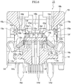
Fig. 4 is a perspective view of the IC socket showing a state in which an operating member of the IC socket of the present embodiment takes an ascending uppermost position thereof. -
Fig. 5 is a perspective view of the IC socket, partially cut away, showing a state in which the operating member of the IC socket of the present embodiment takes a descending lowermost position thereof. -
Fig. 6 is a sectional view of the IC socket showing a state in which an IC socket of the IC package of the present embodiment is accommodated in a socket body. -
Fig. 7 is a perspective view of the IC socket showing a state in which the operating member of the IC socket according to the present embodiment is removed. -
Fig. 8 is a perspective view of the IC socket, partially cut away, showing a state in which the operating member of the IC socket according to the present embodiment is removed. -
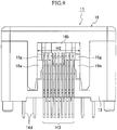
Fig. 9 is a side view of the IC socket showing a state in which the operating member of the IC socket of the present embodiment takes a descending lowermost position thereof. -
Fig. 10 includes perspective views (a) and (b) showing a latch of the IC socket according to the present embodiment, both being viewed from different directions. -
Fig. 11 is a perspective view showing the operating member of the IC socket according to the present embodiment. -
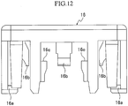
Fig. 12 is a side view showing the operating member of the IC socket according to the present embodiment. -
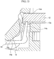
Fig. 13 is a sectional view, in an enlarged scale, showing a state in which the IC package accommodated in the IC socket is slightly pushed upward by a contact pin of the IC socket according to the present embodiment. -
Fig. 14 is a sectional view, in an enlarged scale, showing a state in which the IC package is slightly pressed downward by the pressing force of the latch from the state according to the present embodiment shown inFig. 13 . -
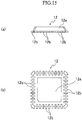
Fig. 15 illustrates the IC package and includes (a) being a front view of the IC package and (b) being a bottom view of the IC package. - Hereunder, an embodiment of the present invention will be described.
-
Figs. 1 to 15 represent one embodiment of the present invention. - Structure or configuration of the present embodiment will be first described hereunder, in which
reference numeral 11 denotes an IC socket as "socket for electric parts", and theIC socket 11 is disposed on a circuit board, not shown, and is a component for establishing an electric connection betweenterminals 12b of anIC package 12 as the "electric parts" and the circuit board for the purpose of performing burn-in test or like of the IC package and the like. - The
IC package 12 has apackage body 12a having a rectangular shape in a plan view as shown inFig. 15 , and a plurality ofterminals 12b are disposed to four sides of the lower surface of the peripheral edge of thepackage body 12a. - On the other hand, the
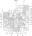
IC socket 11 is provided with, as shown inFigs. 1 and2 , asocket body 13 having anaccommodation surface portion 13a on which theIC package 12 is accommodated,contact pins 14 provided for thesocket body 13 and havingelastic pieces 14a formed withcontact portions 14b contacting terminals 12b of theIC package 12,latches 15 pressing theIC package 12, from the upper side thereof, accommodated in thesocket body 13 to be vertically movable, and anoperating member 16 provided for thesocket body 13 to be vertically movable. When theoperating member 16 is operated to be moved downward, thelatches 15 are rotated (pivoted) in an opening direction, and on the other hand, when theoperating member 16 is moved upward, thelatches 15 are rotated in a closing direction. - The
socket body 13 is formed of a insulated synthetic resin material, and as shown, for example, inFig. 1 andFig. 8 , composed of anupper side member 13e and alower side member 13f. Theupper side member 13e has an upper surface portion formed with theaccommodation surface portion 13a having peripheral four corner portions to which guideportions 13b for guiding theIC package 12 when accommodated are formed so as to project upward. On the other hand, thelower side member 13f of thesocket body 13 provided withmount portions 13c so as to project in four directions as shown inFig. 2 , for example, and a plurality ofcontact pins 14 are attached to themount portions 13c to be detachable from the horizontal side. - Further, each of the
contact pins 14 is formed of a metal material having conductivity in so-called horseshoe-shape, and as shown inFig. 2 , each of thecontact pin 14 has aclamp portion 14c so as to clamp themount portion 13c, projecting horizontally from thesocket body 13, from the vertical sides thereof to be detachable. According to such structure, thecontact pin 14 is detachably mounted to themount portion 13c of thesocket body 13 from the side direction. - Furthermore, as shown in
Fig. 2 , each of thecontact pin 14 has a structure in which theelastic piece 14a extends upward from the outer side end portion of themount portion 13c, and then bent inward so as to substantially horizontally extend, and thecontact portion 14b is formed so as to extend upward from the front end portion of theelastic piece 14a in a manner such that thecontact portion 14b contacts acorresponding terminals 12b of theIC package 12. Thecontact pins 14 are provided withlead portions 14d extending downward from theclamp portions 14c thereof, and thelead portions 14d are inserted into the circuit board, not shown, and then are soldered to be fixed thereto. - In this way, plural contact pins 14 are arranged at four side portions of the peripheral edge of the
socket body 13 to be in parallel with each other and adjacently at a predetermined pitch. - As shown in
Fig. 9 , thelatches 15 are arranged at four portions with respect to the respective sides of theIC package 12 and positioned above the plural contact pins 14 to be rotatable with respect to thesocket body 13. In an operation, when thelatches 15 are in closed state, the upper portion of the peripheral edge portion of theIC package 12 is pressed, and when thelatches 15 are in opened state, theIC package 12 can be accommodated into or taken out of theaccommodation surface portion 13a of thesocket body 13. - More specifically, as shown in
Fig. 10 or others in a plan view, each of thelatch 15 has a front end side portion having a narrow width H1 and a rear end side portion having a wide width H2, thus providing a trapezoid shape. Anopening 15f is formed to a central portion of the trapezoid portion. Rotation (rotating)shafts 15a are located to the front end side of thelatches 15 so as to project in both side directions, and as shown inFig. 8 , bothside rotation shafts 15a are clamped and held between theupper side member 13e and thelower side member 13f to be rotatable. Therotation shafts 15a (fulcrum) are positioned below the IC packageaccommodation surface portion 13a of thesocket body 13. - Furthermore, each of the
latches 15 is formed with acam portion 15c between a pair ofrotation shafts 15a located on both sides on the same axis, and as shown inFig. 2 showing the left-half side of thelatch 15, when thelatch 15 is rotated in the opening direction, theelastic piece 14a of thecontact pin 14 is pressed by thecam portion 15c and is hence elastically deformed downward, thecontact portion 14b is displaced downward so as to be separated in the downward direction from the contacting portion to the terminal 12b of theIC package 12. Likely, as shown inFig. 2 showing the right-half side of thelatch 15 andFig. 6 , when thelatch 15 is rotated in the closing direction, the pressing force of thecam portion 15c to theelastic piece 14a is released and thecontact portion 14b is displaced upward by the elastic force of theelastic piece 14a to thereby move thecontact portion 14b to the contacting portion of the terminal 12b of theIC package 12. - On an opposite side to the
cam portion 15c, aninclined surface portion 15h for escape is formed on an extension of the axis of therotation shaft 15a, and according to such formation of theinclined surface portion 15h, the sectional area of thecam portion 15c is made smaller than that of therotation shaft 15a on each of both sides of thelatch 15. - Moreover, as shown in
Figs. 2 and10 , for example, thelatch 15 is provided with thepressing portion 15d (fulcrum point) pressing the upper surface of theIC package 12, and in addition, anoperation portion 15e (point of effort) to be operated for opening which is pressed downward at a descending time of the operatingmember 16. When theoperation portion 15e to be operated for opening is pressed downward, thelatch 15 is rotated in the opening direction. - The
operation portion 15e to be operated for opening is formed at substantially the central portion on the rear end side, at which the width H2 of thelatch 15 is widened, and on the outer edge side of theopening 15f. - As shown in
Fig. 2 , a part of the rear end portion of thelatch 15, at which theoperation portion 15e to be operated for opening is formed, has asurface 15j facing the contact pins 14. Thesurface 15j curves along the curved-shape portions 14f of the contact pins 14. Therefore, when thelatch 15 is opened, the part of which theoperation portion 15e to be operated for opening is formed become in parallel with the curved-shape portions 14f of the contact pins 14. As a result, a strength of the rear end of thelatch 15 can be improved by effectively using a space between the curve-shapedportion 14f of the contact pins 14 and thesurface 15j of thelatch 15. - Furthermore, a pair of
operation portions 15g (points of effort) to be operated for closing are formed so as to project sideway at both end portions of the rear end side at which the width H2 of the latch is widened (seeFig. 10 ). The pairedoperation portions 15g to be operated for closing are formed so as to project sideway near the outer sides of the arrangement range width H3 of the contact pins 14 arranged, and according to this arrangement, a distance H2 between bothoperation portions 15g to be operated for closing is widened more than the arrangement range width H3 (for example, seeFig. 9 ). - Still furthermore, the operating
member 16 has a frame-shaped structure in a plan view and is provided for thesocket body 13 to be vertically movable. The operatingmember 16 is urged upward (seeFig. 3 ) bysprings 17 which are disposed at four positions, and, at the uppermost position, an engagingportion 16a shown inFig. 11 is engaged with aportion 13d to be engaged (engagement portion 13d shown inFig. 7 ) formed to thesocket body 13 to thereby restrict the upward movement of the operatingmember 16. - Furthermore, the operating
member 16 is provided with the operatingportion 16b for opening which rotates thelatch 15 in the opening direction thereof in engagement with theoperation portion 15e to be operated for opening formed to the central portion in the width direction of thelatch 15 when the operatingmember 16 is moved downward from the uppermost position thereof, that is, the operatingmember 16 is moved from the state shown in right-half state inFig. 2 to the left-half state therein. The operatingportion 16b for opening is provided for the operatingmember 16 so as to extend in an extending direction toward the obliquely downward inside thesocket body 13. - The operating
portion 16b for opening comprises aslide surface 16c linearly formed so as to presses and slides theoperation portion 15e to be operated for opening of thelatch 15 as shown inFig. 2 , for example. The operatingportion 16b for opening is formed so as to, when the operatingportion 16b for opening of the openingmember 16 is moved downward, the operatingportion 16b is inserted into theopening portion 15f while pressing downward aoperation portion 15g to be operated for closing of thelatch 15. - In the state where the operating
member 16 is moved downward to the descending lowermost position and thelatch 15 is fully opened, it is set that the front end of the operatingportion 16b for opening is inserted into theopening 15f to a position on an extension axis line of therotation shaft 15a, and afront end surface 16d along the perpendicular direction of the operatingportion 16b for opening approximately abuts against theinclined surface portion 15h for escape of thelatch 15. - Still furthermore, as shown in
Fig. 4 , the operatingmember 16 is formed with a pair ofoperating portions 16e for closing, and when the operatingmember 16 is moved upward from the most lowering position, a pair ofoperation portions 15g to be operated for closing of thelatch 15 is pressed upward to close thelatch 15 by the pair of the operatingportions 16e for closing. The operatingportions 16e for closing are disposed on both sides of the arranged contact pins 14 and on the inside portion from the mostoutside portion 14e of the horseshoe-shaped contact pins 14 (seeFig. 2 ). - Incidentally, the
IC socket 11 of the structure mentioned above is not provided with a floating plate which is provided in a conventional structure. - Hereunder, a method of using the
IC socket 11 of the structure mentioned above will be explained. - In the following, there will be explained a case in which the
IC package 12 is accommodated on theIC socket 11 in a state in which theIC socket 11 is preliminarily fixed to a circuit board. - First, when the operating
member 16 is pressed downward against the urging force of thesprings 17 from the states shown in right-half inFig. 2 andFig. 4 , theoperation portions 15e to be operated for opening of thelatches 15 are pressed while sliding on the slidingsurface 16c of the operatingportion 16b for opening of the operatingmember 16, and thelatches 15 are then rotated in the opening direction thereof with therotation shafts 15a being the center of the rotation. According to this motion, the operatingportion 16b for opening of the operatingmember 16 is deeply inserted into theopening portion 15f of thelatch 15, and thepressing portion 15d of thelatch 15 is retired from the accommodation/take-out range of the IC package 12 (see left-half side inFig. 2 ). - As described above, since there is provided the operating
member 16 having the operatingportion 16b for opening for rotating thelatch 15 in the opening direction thereof by pressing downward theoperation portion 15e to be operated for opening formed to the central portion in the width direction of thelatch 15, spaces on both the sides of the latch can be made narrow in comparison with a structure in which the latch is pressed downward by using spaces on both the sides of thelatch 15, thus contributing realization of compact outer configuration of theIC socket 11. - Furthermore, the
opening portion 15f is formed to the central portion of thelatch 15, and when the operatingportion 16b for opening of the operatingmember 16 is moved downward, the operatingportion 16b is inserted into theopening portion 15f while pressing downward theoperation portion 15e to be operated for opening formed to the rear side of theopening 15f of thelatch 15. According to such structure, the operatingmember 16 is formed to be further on the inner side of thesocket body 13, thus also realizing the compact outer configuration of theIC socket 11. - Still furthermore, as shown in
Fig. 2 , the operatingportion 16b for opening of the operatingmember 16 is provided with the slidingsurface 16c, formed linearly, pressing theoperation portion 15e to be operated for opening of thelatch 15 so as to slide on the slidingsurface 16c. Accordingly, in comparison with the slidingsurface 16c having a curved- or bent-shape, the outer configuration of the operating member can be further made compact with the desired amount of the rotating motion of thelatch 15 being ensured. - Still furthermore, the
latch 15 is formed with a pair ofrotation shafts 15a on both the sides of theopening portion 15f, and in the most lowering position of the operatingmember 16, the front end portion of the operatingportion 16b is inserted to a position of theopening portion 15f on the extension line of therotation shaft 15a. According to such structure, the operatingmember 16 is provided to the position further on the inner side of thesocket body 13, thus also making compact the outer configuration of theIC socket 11. - In the state in which the
latch 15 is opened maximally, the front end portion of the operatingportion 16b for opening of the operatingmember 16 is inserted into theopening portion 15f of thelatch 15 deeply to a position on the extension axis line of therotation shaft 15a, so that thefront end surface 16d along the perpendicular direction of the operatingportion 16b for opening almost abuts against theinclined surface portion 15h for escape of thelatch 15. According to such setting, the outer configuration can be made extremely compact with the amount of rotational motion of thelatch 15 being ensured (see left-half side inFig. 2 andFig. 5 ). - A most
outside position 15i in a state where thelatch 15 is maximally opened takes a position almost not projecting from the mostoutside portion 14e of thecontact pin 14 as shown in the left-half side inFig. 2 , which is different from a conventional structure, and does not project largely outside. Accordingly, the outer configuration of theIC socket 11 can be extremely downsized, thus realizing a compact structure of theIC socket 11. - Furthermore, since the rotation center of the
rotation shaft 15a of thelatch 15 is positioned below the IC packageaccommodation surface portion 13a of thesocket body 13, the stroke of thelatch 15 to theaccommodation surface portion 13a can be made longer, so that even if the rotating amount of thelatch 15 is small, theIC package 12 can be pressed and/or released by the movement of thepressing portion 15d. Thus, the vertical stroke of the operatingmember 16 can be made short, and hence, the vertical stroke of theIC socket 11 can be made also short, thus making compact the structure of the operatingmember 16. - In addition, since the moving amount in the outside direction of the
latch 15 can be shortened, theIC socket 11 can be made compact. - Incidentally, according to the rotation of the
latch 15, theelastic piece 14a of thecontact pin 14 is pressed by thecam portion 15c of thelatch 15 and then elastically deformed downward. According to this pressing operation, thecontact portion 14b of thecontact pin 14 is displaced or urged downward. - Under the state mentioned above, the
IC package 12 is delivered by an automatic machine. Then, the IC package is guided by theguide portions 13b of thesocket body 13 and is accommodated to a predetermined position on the IC packageaccommodation surface portion 13a of thesocket body 13 which is not provided with any floating plate. - Thereafter, when the external force, which has applied to the operating
member 16, is released, the operatingmember 16 is moved upward by the urging force of thesprings 17, and according to this upward motion of the operatingmember 16, theoperation portions 15g to be operated for closing of thelatches 15 are pushed upward by a pair of the operatingportion 16e for closing positioned on both the sides of a plurality of the contact pins 14 and then, thelatches 15 are rotated in the closing direction thereof. - As explained above, as shown in
Figs. 4 and9 , according to the structure in which the pairedoperation portions 15g for closing of thelatches 15 are formed so as to project on both the sides of the alignment of the plural contact pins 14, and the pairedoperating portions 16e for closing of the operatingmember 16 are positioned on both the sides of the alignment of the contact pins 14, it becomes unnecessary to provide a pair of the operatingportions 16e for closing of the operatingmember 16 outside the contact pins 14 (see right-half side inFig. 2 ). Thus, in this viewpoint, the outer configuration of the operatingmember 16, i.e.,socket body 13, can be also made compact. - On the other hand, when the
latches 15 are rotated in the closing direction, the pressing force by thecam portions 15c of thelatch 15 to theelastic pieces 14a of the contact pins 14 is released, theelastic pieces 14a are displaced upward by the elastic force, and thecontact portions 14b then contact theterminals 12b of theIC package 12, respectively. According to such motion, theIC package 12 is moved slightly upward from the IC packageaccommodation surface portion 13a of thesocket body 13 by the elastic force of theelastic pieces 14a (seeFig. 13 ). - Thereafter, the operating
member 16 is moved further upward while thelatches 15 being closed, and the upper surface of theIC package 12 is thereby pressed downward by thepressing portions 15d of thelatches 15. - Then, as shown in
Fig. 14 , theIC package 12 is moved slightly downward against the urging force of theelastic pieces 14a of the contact pins 14. - According to such motion, the
IC package 12 is electrically connected to the circuit board through thecontact pin 14 so as to be ready for performing a burn-in test. - According to the configuration mentioned above, it becomes unnecessary to vertically move the seating surface (
accommodation surface portion 13a) of theIC package 12 by thecam portion 15c of thelatch 15. In addition, theelastic pieces 14a of the contact pins 14 is formed so as to elastically deformed. Therefore, it becomes unnecessary to locate any floating plate. Thus, the pushing amount of theIC package 12 by thepressing portion 15d of thelatch 15 can be made small, and accordingly, a distance from the rotating center (pivot center) of thelatch 15 to thepressing portion 15d thereof can be shortened, and thelatch 15 can be hence made compact, resulting in realization of thecompact IC socket 11. - Still furthermore, since becomes unnecessary to locate the floating plate, the number of parts to be arranged can be reduced. Accordingly, tolerance of each of parts or components can be made small. Additionally, vibrations in the lateral direction on a plane, which occurs in the case the floating plate is used, can be prevented. Thus, the
IC package 12 can be arranged to a predetermined position more precisely. - As described above, when the
IC package 12 is accommodated to theIC socket 11, thelatches 15 are rotated in the direction to be opened, and so theelastic pieces 14a of the contact pins 14 move downward. After this, IC package is accommodated, then, theelastic pieces 14a moves upward so that thecontact portions 14b contact with theterminals 12b of theIC package 12. Therefore, in comparison with the conventional art, the present embodiment can make eachcontact portion 14b contact with the terminal 12b at pinpoint contact and any wiping is hardly caused. Hence, according to the present embodiment, any wiping trail or trace is not almost caused to the terminal 12b of theIC package 12, and in addition, thecontact portions 14b of the contact pins 14 are hard to come away even in a case of theIC package 12 having extremely narrow width. - In addition, any wiping trail or trace is not almost caused to the upper surface of the
IC package 12 because any sliding is hardly caused when thelatches 15 press the upper surface of theIC package 12. - Furthermore, as mentioned above, when a test of the
IC package 12 finishes and theIC package 12 is picked up, thelatches 15 are gradually opened and so thecam portions 15c of thelatches 15 make theelastic pieces 14a of the contact pins 14 move downward. Consequently, the present embodiment can certainly prevent thecontact portions 14b of the contact pins 14 from sticking with theterminals 12b of theIC package 12. - Moreover, since the latch has so-called a trapezoid shape having a front end side (inside) having a narrow width H1 and a rear end side (outside) having a wide width H2, and a center side (
operation portion 15e to be operated for opening) is constructed for an opening portion, and both end sides (operation portions 15g to be operated for closing) are constructed for closing portions, it is not necessary to form or provide a structure for opening/closing the latch in a space on the rear side of thelatch 15, thereby making further compact the entire outer configuration of theIC socket 11. - Still furthermore, since the clamping
portions 14c of the contact pins 14 can be provided to be detachable to themount portion 13c of thesocket body 13 from the transverse side of thesocket body 13, operation workings such as exchanging working can be extremely easily done. - Still furthermore, the
operation portions 15e to be operated for opening of thelatches 15 are arranged at the central portions in the width direction thereof so that theseportions 15e are opened by the pressing of the operatingportions 16b for opening of the operatingmember 16, and accordingly, thelatches 15 can perform the opening and/or closing operation in a balanced state only by pressing one portion of the operatingmember 16. - Further, it is to be noted that in the above described embodiment, although the present invention is applied to the
IC socket 11 as "socket for electric parts", the present invention is not limited to this application and is applicable to other devices and the like.
Claims (4)
- A socket (11) for electric parts (12) comprising:a) a socket body (13) which has a rectangle shape and an accommodation surface (13a) to accommodate an electric part (12) having a rectangle shape and a lower surface to which terminals (12b) are provided;b) plural contact pins (14), wherein each of which has an elastic piece (14a) to contact with the terminals (12b) of the electric part (12);c) a latch (15) rotatably disposed on the socket body (13) so as to positioned above the contact pins (14), which presses an upper part of peripheral portion of the electric part (12) when the latch (15) is closed, and the electric part (12) is able to be accommodated onto and taken out from the accommodation surface (13a) when the latch (15) is opened, andd) an operating member (16) which is vertically movably disposed in the socket body (13), and comprises an operating portion for opening (16b) constituted so as to press down an operation portion to be operated for opening (15e) of the latch (15) and rotate the latch (15) in an opening direction when the operating member (16) moves downward,characterized in that the contact pins (14) are horseshoe shaped and are disposed in parallel and at predetermined intervals to a peripheral edge of the socket body (13) and that a most outside position (15i) of the latch (15) is disposed on an inside of most outside portion (14e) of the contact pins (14) when the latch (15) is opened to an outermost position.
- The socket (11) for electric parts (12) according to claim 1, wherein the most outside position (15i) of the latch (15) is defined by the operation portion to be operated for opening (15e).
- The socket (11) for electric parts (12) according to claims 1 or 2, wherein a rotation shaft (15a) of the latch (15) is positioned below the accommodation surface (13a) of the socket body (13).
- The socket (11) for electric parts (12) according to any one of claims 1 to 3, wherein the operation portion to be operated for opening (15e) formed at a rear end side of the latch (15) has a surface (15j) which faces the contact pins (14) and curves along curved-shape portions (14f) of the contact pins (14).
Applications Claiming Priority (1)
| Application Number | Priority Date | Filing Date | Title |
|---|---|---|---|
| JP2011288139A JP5836113B2 (en) | 2011-12-28 | 2011-12-28 | Socket for electrical parts |
Publications (3)
| Publication Number | Publication Date |
|---|---|
| EP2611271A2 EP2611271A2 (en) | 2013-07-03 |
| EP2611271A3 EP2611271A3 (en) | 2016-11-02 |
| EP2611271B1 true EP2611271B1 (en) | 2018-02-07 |
Family
ID=47458669
Family Applications (1)
| Application Number | Title | Priority Date | Filing Date |
|---|---|---|---|
| EP12197416.6A Not-in-force EP2611271B1 (en) | 2011-12-28 | 2012-12-17 | Socket for electric parts |
Country Status (4)
| Country | Link |
|---|---|
| US (1) | US8721358B2 (en) |
| EP (1) | EP2611271B1 (en) |
| JP (1) | JP5836113B2 (en) |
| CN (1) | CN103187650B (en) |
Families Citing this family (3)
| Publication number | Priority date | Publication date | Assignee | Title |
|---|---|---|---|---|
| WO2012133740A1 (en) * | 2011-03-31 | 2012-10-04 | 株式会社エンプラス | Socket for electric component |
| JP5886032B2 (en) * | 2011-12-26 | 2016-03-16 | 株式会社エンプラス | Socket for electrical parts |
| JP6150681B2 (en) * | 2013-08-29 | 2017-06-21 | 株式会社エンプラス | Upper plate biasing unit and socket for electrical parts |
Family Cites Families (9)
| Publication number | Priority date | Publication date | Assignee | Title |
|---|---|---|---|---|
| JP2667633B2 (en) * | 1994-02-24 | 1997-10-27 | 山一電機株式会社 | IC holding device in IC socket |
| JP2954560B2 (en) * | 1998-01-14 | 1999-09-27 | 山一電機株式会社 | IC socket |
| JP4467404B2 (en) * | 2004-10-29 | 2010-05-26 | 株式会社エンプラス | Socket for electrical parts |
| JP4729346B2 (en) * | 2005-06-30 | 2011-07-20 | 株式会社エンプラス | Socket for electrical parts |
| JP4676841B2 (en) | 2005-08-23 | 2011-04-27 | 株式会社エンプラス | Socket for electrical parts |
| JP2007109607A (en) * | 2005-10-17 | 2007-04-26 | Three M Innovative Properties Co | Socket for electronic device |
| CN201054407Y (en) * | 2007-05-22 | 2008-04-30 | 富士康(昆山)电脑接插件有限公司 | Electric connector |
| JP5029969B2 (en) * | 2008-11-12 | 2012-09-19 | 山一電機株式会社 | Electrical connection device |
| JP5140659B2 (en) * | 2009-12-25 | 2013-02-06 | 株式会社エンプラス | Socket for electrical parts |
-
2011
- 2011-12-28 JP JP2011288139A patent/JP5836113B2/en active Active
-
2012
- 2012-12-13 US US13/713,303 patent/US8721358B2/en active Active
- 2012-12-17 EP EP12197416.6A patent/EP2611271B1/en not_active Not-in-force
- 2012-12-20 CN CN201210560636.2A patent/CN103187650B/en active Active
Non-Patent Citations (1)
| Title |
|---|
| None * |
Also Published As
| Publication number | Publication date |
|---|---|
| EP2611271A2 (en) | 2013-07-03 |
| US20130171861A1 (en) | 2013-07-04 |
| CN103187650A (en) | 2013-07-03 |
| JP2013137926A (en) | 2013-07-11 |
| US8721358B2 (en) | 2014-05-13 |
| EP2611271A3 (en) | 2016-11-02 |
| CN103187650B (en) | 2016-08-24 |
| JP5836113B2 (en) | 2015-12-24 |
Similar Documents
| Publication | Publication Date | Title |
|---|---|---|
| EP2611270B1 (en) | Socket for electric parts | |
| US6439910B2 (en) | Rotatable guide member for a socket for electrical parts | |
| KR20160103015A (en) | Electric component socket | |
| US6743034B2 (en) | Socket for electrical parts | |
| EP2611271B1 (en) | Socket for electric parts | |
| EP2573884B1 (en) | Socket for electric component | |
| EP2611269B1 (en) | Socket for electric parts | |
| US6857888B2 (en) | Socket for electrical parts | |
| JP4180906B2 (en) | Contact pin, contact pin molding method, and socket for electrical parts | |
| US6768653B2 (en) | Mount structure | |
| JP3822074B2 (en) | Socket for electrical parts | |
| JP5487045B2 (en) | Socket for electrical parts | |
| JP3730020B2 (en) | Socket for electrical parts | |
| JP2017027758A (en) | Socket for electrical component | |
| SG186517A1 (en) | Card connector | |
| JP3776338B2 (en) | Socket for electrical parts | |
| JP4322461B2 (en) | Socket for electrical parts | |
| JP3717674B2 (en) | Socket for electrical parts | |
| US9343836B2 (en) | Electrical socket having improved cam | |
| US20080278919A1 (en) | Socket for electric component | |
| JP2001023745A (en) | Socket for electric component | |
| JP2003323956A (en) | Socket for electrical component | |
| JP2002246093A (en) | Contact pin and ic socket |
Legal Events
| Date | Code | Title | Description |
|---|---|---|---|
| PUAI | Public reference made under article 153(3) epc to a published international application that has entered the european phase |
Free format text: ORIGINAL CODE: 0009012 |
|
| AK | Designated contracting states |
Kind code of ref document: A2 Designated state(s): AL AT BE BG CH CY CZ DE DK EE ES FI FR GB GR HR HU IE IS IT LI LT LU LV MC MK MT NL NO PL PT RO RS SE SI SK SM TR |
|
| AX | Request for extension of the european patent |
Extension state: BA ME |
|
| PUAL | Search report despatched |
Free format text: ORIGINAL CODE: 0009013 |
|
| AK | Designated contracting states |
Kind code of ref document: A3 Designated state(s): AL AT BE BG CH CY CZ DE DK EE ES FI FR GB GR HR HU IE IS IT LI LT LU LV MC MK MT NL NO PL PT RO RS SE SI SK SM TR |
|
| AX | Request for extension of the european patent |
Extension state: BA ME |
|
| RIC1 | Information provided on ipc code assigned before grant |
Ipc: H05K 7/10 20060101AFI20160928BHEP |
|
| 17P | Request for examination filed |
Effective date: 20170502 |
|
| RBV | Designated contracting states (corrected) |
Designated state(s): AL AT BE BG CH CY CZ DE DK EE ES FI FR GB GR HR HU IE IS IT LI LT LU LV MC MK MT NL NO PL PT RO RS SE SI SK SM TR |
|
| GRAP | Despatch of communication of intention to grant a patent |
Free format text: ORIGINAL CODE: EPIDOSNIGR1 |
|
| INTG | Intention to grant announced |
Effective date: 20170727 |
|
| GRAJ | Information related to disapproval of communication of intention to grant by the applicant or resumption of examination proceedings by the epo deleted |
Free format text: ORIGINAL CODE: EPIDOSDIGR1 |
|
| GRAR | Information related to intention to grant a patent recorded |
Free format text: ORIGINAL CODE: EPIDOSNIGR71 |
|
| GRAS | Grant fee paid |
Free format text: ORIGINAL CODE: EPIDOSNIGR3 |
|
| GRAA | (expected) grant |
Free format text: ORIGINAL CODE: 0009210 |
|
| INTC | Intention to grant announced (deleted) | ||
| INTG | Intention to grant announced |
Effective date: 20171220 |
|
| AK | Designated contracting states |
Kind code of ref document: B1 Designated state(s): AL AT BE BG CH CY CZ DE DK EE ES FI FR GB GR HR HU IE IS IT LI LT LU LV MC MK MT NL NO PL PT RO RS SE SI SK SM TR |
|
| REG | Reference to a national code |
Ref country code: GB Ref legal event code: FG4D |
|
| REG | Reference to a national code |
Ref country code: AT Ref legal event code: REF Ref document number: 969251 Country of ref document: AT Kind code of ref document: T Effective date: 20180215 Ref country code: CH Ref legal event code: EP |
|
| REG | Reference to a national code |
Ref country code: IE Ref legal event code: FG4D |
|
| REG | Reference to a national code |
Ref country code: DE Ref legal event code: R096 Ref document number: 602012042627 Country of ref document: DE |
|
| REG | Reference to a national code |
Ref country code: NL Ref legal event code: MP Effective date: 20180207 |
|
| REG | Reference to a national code |
Ref country code: AT Ref legal event code: MK05 Ref document number: 969251 Country of ref document: AT Kind code of ref document: T Effective date: 20180207 |
|
| PG25 | Lapsed in a contracting state [announced via postgrant information from national office to epo] |
Ref country code: ES Free format text: LAPSE BECAUSE OF FAILURE TO SUBMIT A TRANSLATION OF THE DESCRIPTION OR TO PAY THE FEE WITHIN THE PRESCRIBED TIME-LIMIT Effective date: 20180207 Ref country code: CY Free format text: LAPSE BECAUSE OF FAILURE TO SUBMIT A TRANSLATION OF THE DESCRIPTION OR TO PAY THE FEE WITHIN THE PRESCRIBED TIME-LIMIT Effective date: 20180207 Ref country code: NL Free format text: LAPSE BECAUSE OF FAILURE TO SUBMIT A TRANSLATION OF THE DESCRIPTION OR TO PAY THE FEE WITHIN THE PRESCRIBED TIME-LIMIT Effective date: 20180207 Ref country code: HR Free format text: LAPSE BECAUSE OF FAILURE TO SUBMIT A TRANSLATION OF THE DESCRIPTION OR TO PAY THE FEE WITHIN THE PRESCRIBED TIME-LIMIT Effective date: 20180207 Ref country code: LT Free format text: LAPSE BECAUSE OF FAILURE TO SUBMIT A TRANSLATION OF THE DESCRIPTION OR TO PAY THE FEE WITHIN THE PRESCRIBED TIME-LIMIT Effective date: 20180207 Ref country code: NO Free format text: LAPSE BECAUSE OF FAILURE TO SUBMIT A TRANSLATION OF THE DESCRIPTION OR TO PAY THE FEE WITHIN THE PRESCRIBED TIME-LIMIT Effective date: 20180507 Ref country code: FI Free format text: LAPSE BECAUSE OF FAILURE TO SUBMIT A TRANSLATION OF THE DESCRIPTION OR TO PAY THE FEE WITHIN THE PRESCRIBED TIME-LIMIT Effective date: 20180207 |
|
| PG25 | Lapsed in a contracting state [announced via postgrant information from national office to epo] |
Ref country code: BG Free format text: LAPSE BECAUSE OF FAILURE TO SUBMIT A TRANSLATION OF THE DESCRIPTION OR TO PAY THE FEE WITHIN THE PRESCRIBED TIME-LIMIT Effective date: 20180507 Ref country code: LV Free format text: LAPSE BECAUSE OF FAILURE TO SUBMIT A TRANSLATION OF THE DESCRIPTION OR TO PAY THE FEE WITHIN THE PRESCRIBED TIME-LIMIT Effective date: 20180207 Ref country code: AT Free format text: LAPSE BECAUSE OF FAILURE TO SUBMIT A TRANSLATION OF THE DESCRIPTION OR TO PAY THE FEE WITHIN THE PRESCRIBED TIME-LIMIT Effective date: 20180207 Ref country code: RS Free format text: LAPSE BECAUSE OF FAILURE TO SUBMIT A TRANSLATION OF THE DESCRIPTION OR TO PAY THE FEE WITHIN THE PRESCRIBED TIME-LIMIT Effective date: 20180207 Ref country code: PL Free format text: LAPSE BECAUSE OF FAILURE TO SUBMIT A TRANSLATION OF THE DESCRIPTION OR TO PAY THE FEE WITHIN THE PRESCRIBED TIME-LIMIT Effective date: 20180207 Ref country code: GR Free format text: LAPSE BECAUSE OF FAILURE TO SUBMIT A TRANSLATION OF THE DESCRIPTION OR TO PAY THE FEE WITHIN THE PRESCRIBED TIME-LIMIT Effective date: 20180508 Ref country code: IS Free format text: LAPSE BECAUSE OF FAILURE TO SUBMIT A TRANSLATION OF THE DESCRIPTION OR TO PAY THE FEE WITHIN THE PRESCRIBED TIME-LIMIT Effective date: 20180607 Ref country code: SE Free format text: LAPSE BECAUSE OF FAILURE TO SUBMIT A TRANSLATION OF THE DESCRIPTION OR TO PAY THE FEE WITHIN THE PRESCRIBED TIME-LIMIT Effective date: 20180207 |
|
| PG25 | Lapsed in a contracting state [announced via postgrant information from national office to epo] |
Ref country code: EE Free format text: LAPSE BECAUSE OF FAILURE TO SUBMIT A TRANSLATION OF THE DESCRIPTION OR TO PAY THE FEE WITHIN THE PRESCRIBED TIME-LIMIT Effective date: 20180207 Ref country code: RO Free format text: LAPSE BECAUSE OF FAILURE TO SUBMIT A TRANSLATION OF THE DESCRIPTION OR TO PAY THE FEE WITHIN THE PRESCRIBED TIME-LIMIT Effective date: 20180207 Ref country code: AL Free format text: LAPSE BECAUSE OF FAILURE TO SUBMIT A TRANSLATION OF THE DESCRIPTION OR TO PAY THE FEE WITHIN THE PRESCRIBED TIME-LIMIT Effective date: 20180207 Ref country code: IT Free format text: LAPSE BECAUSE OF FAILURE TO SUBMIT A TRANSLATION OF THE DESCRIPTION OR TO PAY THE FEE WITHIN THE PRESCRIBED TIME-LIMIT Effective date: 20180207 |
|
| REG | Reference to a national code |
Ref country code: DE Ref legal event code: R097 Ref document number: 602012042627 Country of ref document: DE |
|
| PG25 | Lapsed in a contracting state [announced via postgrant information from national office to epo] |
Ref country code: DK Free format text: LAPSE BECAUSE OF FAILURE TO SUBMIT A TRANSLATION OF THE DESCRIPTION OR TO PAY THE FEE WITHIN THE PRESCRIBED TIME-LIMIT Effective date: 20180207 Ref country code: SM Free format text: LAPSE BECAUSE OF FAILURE TO SUBMIT A TRANSLATION OF THE DESCRIPTION OR TO PAY THE FEE WITHIN THE PRESCRIBED TIME-LIMIT Effective date: 20180207 Ref country code: SK Free format text: LAPSE BECAUSE OF FAILURE TO SUBMIT A TRANSLATION OF THE DESCRIPTION OR TO PAY THE FEE WITHIN THE PRESCRIBED TIME-LIMIT Effective date: 20180207 Ref country code: CZ Free format text: LAPSE BECAUSE OF FAILURE TO SUBMIT A TRANSLATION OF THE DESCRIPTION OR TO PAY THE FEE WITHIN THE PRESCRIBED TIME-LIMIT Effective date: 20180207 |
|
| PLBE | No opposition filed within time limit |
Free format text: ORIGINAL CODE: 0009261 |
|
| STAA | Information on the status of an ep patent application or granted ep patent |
Free format text: STATUS: NO OPPOSITION FILED WITHIN TIME LIMIT |
|
| 26N | No opposition filed |
Effective date: 20181108 |
|
| PG25 | Lapsed in a contracting state [announced via postgrant information from national office to epo] |
Ref country code: SI Free format text: LAPSE BECAUSE OF FAILURE TO SUBMIT A TRANSLATION OF THE DESCRIPTION OR TO PAY THE FEE WITHIN THE PRESCRIBED TIME-LIMIT Effective date: 20180207 |
|
| REG | Reference to a national code |
Ref country code: CH Ref legal event code: PL |
|
| GBPC | Gb: european patent ceased through non-payment of renewal fee |
Effective date: 20181217 |
|
| PG25 | Lapsed in a contracting state [announced via postgrant information from national office to epo] |
Ref country code: LU Free format text: LAPSE BECAUSE OF NON-PAYMENT OF DUE FEES Effective date: 20181217 Ref country code: MC Free format text: LAPSE BECAUSE OF FAILURE TO SUBMIT A TRANSLATION OF THE DESCRIPTION OR TO PAY THE FEE WITHIN THE PRESCRIBED TIME-LIMIT Effective date: 20180207 |
|
| REG | Reference to a national code |
Ref country code: IE Ref legal event code: MM4A |
|
| REG | Reference to a national code |
Ref country code: BE Ref legal event code: MM Effective date: 20181231 |
|
| PG25 | Lapsed in a contracting state [announced via postgrant information from national office to epo] |
Ref country code: FR Free format text: LAPSE BECAUSE OF NON-PAYMENT OF DUE FEES Effective date: 20181231 Ref country code: IE Free format text: LAPSE BECAUSE OF NON-PAYMENT OF DUE FEES Effective date: 20181217 |
|
| PG25 | Lapsed in a contracting state [announced via postgrant information from national office to epo] |
Ref country code: BE Free format text: LAPSE BECAUSE OF NON-PAYMENT OF DUE FEES Effective date: 20181231 |
|
| PG25 | Lapsed in a contracting state [announced via postgrant information from national office to epo] |
Ref country code: LI Free format text: LAPSE BECAUSE OF NON-PAYMENT OF DUE FEES Effective date: 20181231 Ref country code: GB Free format text: LAPSE BECAUSE OF NON-PAYMENT OF DUE FEES Effective date: 20181217 Ref country code: CH Free format text: LAPSE BECAUSE OF NON-PAYMENT OF DUE FEES Effective date: 20181231 |
|
| PG25 | Lapsed in a contracting state [announced via postgrant information from national office to epo] |
Ref country code: MT Free format text: LAPSE BECAUSE OF NON-PAYMENT OF DUE FEES Effective date: 20181217 |
|
| PG25 | Lapsed in a contracting state [announced via postgrant information from national office to epo] |
Ref country code: TR Free format text: LAPSE BECAUSE OF FAILURE TO SUBMIT A TRANSLATION OF THE DESCRIPTION OR TO PAY THE FEE WITHIN THE PRESCRIBED TIME-LIMIT Effective date: 20180207 |
|
| PG25 | Lapsed in a contracting state [announced via postgrant information from national office to epo] |
Ref country code: PT Free format text: LAPSE BECAUSE OF FAILURE TO SUBMIT A TRANSLATION OF THE DESCRIPTION OR TO PAY THE FEE WITHIN THE PRESCRIBED TIME-LIMIT Effective date: 20180207 |
|
| PG25 | Lapsed in a contracting state [announced via postgrant information from national office to epo] |
Ref country code: HU Free format text: LAPSE BECAUSE OF FAILURE TO SUBMIT A TRANSLATION OF THE DESCRIPTION OR TO PAY THE FEE WITHIN THE PRESCRIBED TIME-LIMIT; INVALID AB INITIO Effective date: 20121217 Ref country code: MK Free format text: LAPSE BECAUSE OF NON-PAYMENT OF DUE FEES Effective date: 20180207 |
|
| PGFP | Annual fee paid to national office [announced via postgrant information from national office to epo] |
Ref country code: DE Payment date: 20201211 Year of fee payment: 9 |
|
| REG | Reference to a national code |
Ref country code: DE Ref legal event code: R119 Ref document number: 602012042627 Country of ref document: DE |
|
| PG25 | Lapsed in a contracting state [announced via postgrant information from national office to epo] |
Ref country code: DE Free format text: LAPSE BECAUSE OF NON-PAYMENT OF DUE FEES Effective date: 20220701 |