EP2611031B1 - Signal filtering - Google Patents
Signal filtering Download PDFInfo
- Publication number
- EP2611031B1 EP2611031B1 EP11196127.2A EP11196127A EP2611031B1 EP 2611031 B1 EP2611031 B1 EP 2611031B1 EP 11196127 A EP11196127 A EP 11196127A EP 2611031 B1 EP2611031 B1 EP 2611031B1
- Authority
- EP
- European Patent Office
- Prior art keywords
- tif
- component
- signal port
- clk
- signal
- Prior art date
- Legal status (The legal status is an assumption and is not a legal conclusion. Google has not performed a legal analysis and makes no representation as to the accuracy of the status listed.)
- Active
Links
- 238000001914 filtration Methods 0.000 title claims description 12
- 238000006243 chemical reaction Methods 0.000 claims description 51
- 230000001419 dependent effect Effects 0.000 claims description 24
- 230000003111 delayed effect Effects 0.000 claims description 13
- 238000000034 method Methods 0.000 claims description 8
- 238000004891 communication Methods 0.000 claims description 3
- 230000010363 phase shift Effects 0.000 description 7
- 238000010586 diagram Methods 0.000 description 6
- 230000003071 parasitic effect Effects 0.000 description 6
- 238000001228 spectrum Methods 0.000 description 6
- 230000001413 cellular effect Effects 0.000 description 2
- XUIMIQQOPSSXEZ-UHFFFAOYSA-N Silicon Chemical compound [Si] XUIMIQQOPSSXEZ-UHFFFAOYSA-N 0.000 description 1
- 230000002238 attenuated effect Effects 0.000 description 1
- 239000000872 buffer Substances 0.000 description 1
- 238000012937 correction Methods 0.000 description 1
- 238000013461 design Methods 0.000 description 1
- 238000004519 manufacturing process Methods 0.000 description 1
- 238000009877 rendering Methods 0.000 description 1
- 230000035945 sensitivity Effects 0.000 description 1
- 229910052710 silicon Inorganic materials 0.000 description 1
- 239000010703 silicon Substances 0.000 description 1
- 230000003595 spectral effect Effects 0.000 description 1
- 238000012360 testing method Methods 0.000 description 1
- 238000012546 transfer Methods 0.000 description 1
- 238000012795 verification Methods 0.000 description 1
Images


Classifications
-
- H—ELECTRICITY
- H04—ELECTRIC COMMUNICATION TECHNIQUE
- H04B—TRANSMISSION
- H04B15/00—Suppression or limitation of noise or interference
-
- H—ELECTRICITY
- H03—ELECTRONIC CIRCUITRY
- H03H—IMPEDANCE NETWORKS, e.g. RESONANT CIRCUITS; RESONATORS
- H03H19/00—Networks using time-varying elements, e.g. N-path filters
- H03H19/008—Networks using time-varying elements, e.g. N-path filters with variable switch closing time
-
- H—ELECTRICITY
- H04—ELECTRIC COMMUNICATION TECHNIQUE
- H04B—TRANSMISSION
- H04B1/00—Details of transmission systems, not covered by a single one of groups H04B3/00 - H04B13/00; Details of transmission systems not characterised by the medium used for transmission
- H04B1/38—Transceivers, i.e. devices in which transmitter and receiver form a structural unit and in which at least one part is used for functions of transmitting and receiving
- H04B1/40—Circuits
-
- H—ELECTRICITY
- H04—ELECTRIC COMMUNICATION TECHNIQUE
- H04W—WIRELESS COMMUNICATION NETWORKS
- H04W84/00—Network topologies
- H04W84/02—Hierarchically pre-organised networks, e.g. paging networks, cellular networks, WLAN [Wireless Local Area Network] or WLL [Wireless Local Loop]
- H04W84/10—Small scale networks; Flat hierarchical networks
- H04W84/12—WLAN [Wireless Local Area Networks]
Definitions
- the present disclosure relates to a signal filter, a down-conversion mixer comprising the signal filter, an up-conversion mixer comprising the signal filter, and a method of filtering a signal, having application in particular, but not exclusively, in wireless communication equipment for transmitting or receiving a radio frequency signal.
- a transferred impedance filter also known as a transferred impedance filter (TIF) utilising N-path filtering techniques, such as disclosed in US 7,187,230 and in " Tunable high-Q N-path band-pass filters: modeling and verification", A. Ghaffari et al, IEEE J. of Solid-State Circuits, May 2011 , can provide narrowband bandpass filtering centred at a switching frequency, that is, a local oscillator frequency.
- a direct delta-sigma receiver is disclosed employing TIFs.
- a known 4-path TIF mixes a signal to a desired bandpass frequency range from odd harmonics of a local oscillator (LO) signal, using a switching duty cycle of 25%.
- the TIF acts as a high impedance for input frequencies close to the switching frequency, forming a high-Q bandpass filter centred at the switching frequency.
- a basic TIF circuit is a capacitively loaded passive mixer, and therefore it will mix signals from all odd harmonics of the LO signal.
- the stopband attenuation of the circuit is limited by the on-resistances of the switches employed in the TIF, and, near odd harmonics of the clock signal, additional bandpass resonances occur.
- the transfer function of such a 4-path TIF has repeated, but slightly attenuated, bandpass responses on every odd harmonic of the LO signal.
- the use of a switching duty cycle shorter than 25% can slightly improve the bandpass frequency selectivity, although attenuation at the odd harmonics of the LO signal is severely degraded, as described by Ghaffari et al.
- phase than four can be used to construct 6 or 8-path TIFs, as disclosed by Ghaffri et al.
- mixing down from odd harmonics of the LO signal can be reduced by using, for example, an 8-path TIF with a 12.5% switching duty cycle. That, however, leads to reduced attenuation at harmonics of the clock signal, rendering the benefits of the circuit rather limited, while significantly increasing the maximum VCO frequency required for generating the LO signal.
- the main reason for the reduced attenuation is the shorter switch on-time, which limits the filtering at odd harmonics of the LO signal, while slightly reducing losses in the desired passband.
- the TIF is usually connected in parallel with a passive LC-resonator, which reduces the losses in the TIF passband, although this is insignificant compared with the losses of the passive LC-resonator. Furthermore, the harmonic rejection capabilities of the LC-resonator alone are not enough for typical applications, for example for wireless local area network (WLAN) coexistence in cellular transceivers.
- WLAN wireless local area network
- EP 2204907 discloses a four-phase TIF driven by LO signals having a duty cycle of about 20%, or less than 25%, and an eight-phase TIF driven by LO signals having a duty cycle of about 12.5% or less.
- a signal filter comprising:
- a method of filtering a signal using a first 4-differential-path transferred impedance filter, TIF having:
- the signal filter may comprise two 4-differential-path TIFs coupled in parallel.
- Each of the TIFs may be clocked with clock signals having four non-overlapping phases and a duty cycle in the range 16.75% to 25%, the phases of the clock signals used for clocking the second TIF being delayed by 45 degrees with respect to the phases of the clock signals used for clocking the first TIF.
- the signal filter and the method of filtering a signal can enable reduced harmonic folding, higher attenuation around odd harmonics of the frequency of the clock signals and reduced sensitivity to phase errors in the clock signals, without requiring an increased oscillator frequency for generating the clock signals.
- the use of differential signal paths can provide rejection of all even harmonics.
- Such a signal filter and method of filtering a signal may be used for radio frequency (RF) narrowband bandpass filtering without inductors, and have application, for example, in low
- RF radio frequency
- the first-TIF first, second, third and fourth clock signals and the second-TIF first, second, third and fourth clock signals may have a duty cycle in the range 20 to 25%, and preferably 25%, that is, a quarter. This can reduce folding from third, fifth, eleventh, thirteen and nineteenth harmonics of the frequency of the clock signal.
- first-TIF first, second, third and fourth clock signals and the second-TIF first, second, third and fourth clock signals may have a duty cycle in the range 16.75 to 20.75%, and preferably 18.75%, that is, three sixteenths. This can enable reduced folding from seventh, ninth, fifteenth and seventeenth order harmonics of the frequency of the clock signal, for example by 15 to 30dB.
- the first and second TIFs can have an identical structure, which can simplify integrated circuit design, manufacture and testing.
- the signal filter may comprise a first transconductance amplifier arranged to deliver to the second component of the second signal port of the first TIF a first current dependent on a voltage difference at the first and third components of the second signal port of the first TIF, and to deliver to the fourth component of the second signal port of the first TIF a second current dependent on a voltage difference at the first and third components of the second signal port of the first TIF; a second transconductance amplifier arranged to deliver to the first component of the second signal port of the first TIF a third current dependent on a voltage difference at the second and fourth components of the second signal port of the first TIF, and to deliver to the third component of the second signal port of the first TIF a fourth current dependent on a voltage difference at the second and fourth components of the second signal port of the first TIF; a third transconductance amplifier arranged to deliver to the second component of the second signal port of the second TIF a fifth current dependent on a voltage difference at the first and third components of the second signal port of the second TIF, and to
- a down-conversion mixer may comprise the signal filter for down-converting an input signal applied to the first differential signal port of the first TIF and to the first differential signal port of the second, and further comprising a combining stage arranged to provide: at a first output of the down-conversion mixer the sum of voltages at the first and second components of the second signal port of the first TIF times a first gain and a voltage at the first component of the second signal port of the second TIF times a second gain, minus voltages at the third and fourth components of the second signal port of the first TIF times the first gain and a voltage at the third component of the second signal port of the second TIF times the second gain; and at a second output of the down-conversion mixer the sum of voltages at the second and third components of the second signal port of the first TIF times the first gain and a voltage at the second component of the second signal port of the second TIF times the second gain, minus voltages at the first and fourth components of the second signal port of the first TIF times the first gain and a voltage at
- a down-conversion mixer can be provided having the advantages described above for the signal filter.
- Such a range of ratios between the first and second gains enables good harmonic rejection.
- the first gain may be unity.
- Such a down-conversion mixer comprising the signal filter, for down-converting an input signal applied to the first differential signal port of the first TIF and to the first differential signal port of the second TIF, may comprise:
- the second gain may be equal to the first gain times 1.5. Such a ratio between the first and second gain can enable improved harmonic rejection.
- the second gain may be equal to the first gain times the square root of two. Such a ratio between the first and second gain can enable further improved harmonic rejection.
- An up-conversion mixer comprising the signal filter, for up-converting an input signal comprising an in-phase component and a quadrature-phase component, may further comprise:
- an up-conversion mixer can be provided having the advantages described above for the signal filter.
- Such a range of ratios between the third drive current and the in-phase component, and between the fourth drive current and the quadrature-phase component, enables good harmonic rejection.
- the first constant may be unity.
- the third drive current may be equal to the in-phase component times the first constant times 1.5
- the fourth drive current may be equal to the quadrature-phase component times the first constant times 1.5.
- the third drive current may be equal to the in-phase component times the first constant times the square root of two
- the fourth drive current may be equal to the quadrature-phase component times the first constant times the square root of two.
- a wireless communication apparatus for example a transmitter, receiver or transceiver, comprising the signal filter.
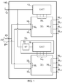
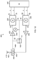
- a signal filter 100 has a filter differential signal port 20 comprising first and second components 20+, 20-.
- the first and second components 20+, 20- of the filter differential signal port 20 are coupled to respective first and second components 32 A+ , 32 A- of a first differential signal port 32 A of a first transferred impedance filter TIF A and to respective first and second components 32 B+ , 32 B- of a first differential signal port 32 B of a second transferred impedance filter TIF B .
- the first transferred impedance filter TIF A has a second signal port 30 A comprising first, second, third and fourth components 30 A,1 , 30 A,2 , 30 A,3 , 30 A,4
- the second transferred impedance filter TIF B has a second signal port 30 B comprising first, second third and fourth components 30 B,1 , 30 B,2 , 30 B,3 , 30 B,4 .
- the first and second transferred impedance filters TIF A , TIF B are four-differential-path transferred impedance filters, that is, each of the first and second transferred impedance filters TIF A , TIF B provides four paths for a differential signal between their respective first differential signal ports 32 A , 32 B and their respective second signal ports 30 A , 30 B .
- a filter clock input 10 for a clock signal is coupled to a first clock generator 12 A and to a second clock generator 12 B .
- the first clock generator 12 A generates first-TIF four-phase, non-overlapping clock signals comprising a first-TIF first-phase clock signal CLK A,I+ having a duty cycle of 25%, a first-TIF second-phase clock signal CLK A,Q , having a phase equal to the phase of the first-TIF first-phase clock signal CLK A,I+ delayed by 90 degrees, a first-TIF third-phase clock signal CLK A,I- having a phase equal to the phase of the first-TIF second-phase clock signal CLK A,Q+ delayed by 90 degrees, and a first-TIF fourth-phase clock signal CLK A,Q- having a phase equal to the phase of the first-TIF third-phase clock signal CLK A,I+ delayed by 90 degrees.
- the first clock generator 12 A may generate the first-TIF four-phase, non-overlapping clock signals using a divide-by-four circuit,
- the first clock generator 12 A is coupled to a first clock port 34 A of the first transferred impedance filter TIF A for delivering the first-TIF four-phase, non-overlapping clock signals.
- the second clock generator 12 B generator comprises a phase shift circuit 14 for generating a delayed LO signal, and a clock circuit 13 coupled to the phase shift circuit 14 for generating second-TIF four-phase, non-overlapping clock signals comprising a second-TIF first-phase clock signal CLK B,I+ having a duty cycle of 25%, a second-TIF first-phase clock signal CK B,Q+ having a phase equal to the phase of the second-TIF first-phase clock signal CLK B,I+ delayed by 90 degrees, a second-TIF third-phase clock signal CLK B,I- having a phase equal to the phase of the second-TIF second-phase clock signal CLK B,Q+ delayed by 90 degrees, and a second-TIF fourth-phase clock signal CLK B,Q- having a phase equal to the phase of the second-TIF third-phase clock signal CLK B,I+ delayed by 90 degrees.
- the phase shift introduced by the phase shift circuit 14 is 45 degrees, that is, one eighth of the period of the LO signal. Therefore, the second-TIF four-phase, non-overlapping clock signals are equal in phase to the first-TIF four-phase, non-overlapping clock signals delayed by 45 degrees.
- the 45-degree time shift may be implemented in the phase shift circuit 14 by inverting the LO signal.
- the LO signal can be a differential signal. Waveforms of the first-TIF and second-TIF four-phase, non-overlapping clock signals are illustrated in Figure 2 .
- the clock circuit 13 may be a copy of the first clock generator 12 A .
- the second clock generator 12 B is coupled to a second clock port 34 B of the second transferred impedance filter TIF B for delivering the second-TIF four-phase, non-overlapping clock signals.
- a preferred duty cycle for the first-TIF and second-TIF four-phase non-overlapping clock signals is 25%, the duty cycle may be in the range 20% to 25%.
- the first transferred impedance filter TIF A comprises first, second, third and fourth differential signal paths P A,1 , P A,2, , P A,3 , P A,4 between the first differential signal port 32 A of the first transferred impedance filter TIF A and the second signal port 30 A of the first transferred impedance filter TIF A , each of these differential signal paths comprising a first component and a second component.
- first component paths of the first, second, third and fourth first-TIF differential signal paths P A,1+ , P A,2+ , P A,3+ , P A,4+ are provided between the first component of the first differential signal port of the first TIF 32 A+ and, respectively, the first, second, third and fourth components of the second signal port of the first TIF 30 A,1 , 30 A,2 , 30 A,3 , 30 A,4 .
- Second component paths of the first, second, third and fourth first-TIF differential signal paths P A,1-, P A,2-, P A,3-, P A,4- are provided between the second component of the first differential signal port of the first TIF 32 A- and, respectively, the third, fourth, first and second components of the second signal port of the first TIF 30 A,3 , 30 A,4 , 30 A,1 , 30 A,2 .
- the first component paths of the first, second, third and fourth first-TIF differential signal paths P A,1+ , P A,2+ , P A,3+ , P A,4+ are selectable by means of, respectively, first-TIF first, second, third and fourth switch elements S A,1 , S A,2 , S A,3 , S A,4 which are coupled in the respective paths, under the control of the first-TIF four-phase, non-overlapping clock signals, and the second component paths of the first, second, third and fourth first-TIF differential signal paths P A,1- , P A,2- , P A,3- , P A,4- are selectable by means of, respectively, first-TIF fifth, sixth, seventh, and eighth switch elements S A,5 , S A,6 , S A,7 , S A,8 which are coupled in the respective paths, under the control of the first-TIF four-phase, non-overlapping clock signals.
- the first-TIF first-phase clock signal CLK A,I+ controls the closure of the first-TIF first and fifth switch elements S A,1 , S A,5 in, respectively, the first and second component paths of the first first-TIF differential signal path P A,1+ , P A,1 .
- the first-TIF second-phase clock signal CLK A,Q+ controls the closure of the first-TIF second and sixth switch elements S A,2 , S A,6 in, respectively, the first and second component paths of the second first-TIF differential signal path P A,2+ , P A,2- .
- the first-TIF third-phase clock signal CLK A,I- controls the closure of the first-TIF third and seventh switch elements S A,3 , S A,7 in, respectively, the first and second component paths of the third first-TIF differential signal path P A,3+ , P A,3- .
- the first-TIF fourth-phase clock signal CLK A,Q- controls the closure of the first-TIF fourth and eighth switch elements S A , 4 , S A,8 in, respectively, the first and second component paths of the fourth first-TIF differential signal path P A,4+ , P A,4- .
- the first transferred impedance filter TIF A also comprises first-TIF first, second, third and fourth capacitive elements C A,1 , C A,2 , C A,3 , C A,4 coupled between a ground and respective ones of the first, second, third and fourth components 30 A,1 , 30 A,2 , 30 A,3 , 30 A,4 of the second signal port 30 A of the first transferred impedance filter TIF A . Therefore, by operation of the first-TIF first to eighth switch elements S A,1 ...S A,8 , two of the first-TIF first to fourth capacitive elements C A,1 ... C A,4 are coupled to the first and second components 20+, 20- of the filter differential signal port 20 throughout operation of the signal filter 100, except for any relatively short periods of non-overlap during periods of changeover between the first TIF four-phase, non-overlapping clock signals.
- the structure of the second transferred impedance filter TIF B is identical to the structure of the first transferred impedance filter TIF A .
- the second transferred impedance filter TIF B comprises first, second, third and fourth differential signal paths P B,1 , P B,2, , P B,3 , P B,4 between the first differential signal port 32 B of the second transferred impedance filter TIF B and the second signal port 30 B of the second transferred impedance filter TIF B , each of these differential signal paths comprising a first component and a second component.
- first component paths of the first, second, third and fourth second-TIF differential signal paths P B,1+ , P B,2+ , P B,3+ , P B,4+ are provided between the first component of the first differential signal port of the second TIF 32 B+ and, respectively, the first, second, third and fourth components of the second signal port of the second TIF 30 B,1 , 30 B,2 , 30 B,3 , 30 B,4 .
- Second component paths of the first, second, third and fourth second-TIF differential signal paths P B,1- , P B,2- , P B,3- , P B,4- are provided between the second component of the first differential signal port of the second TIF 32 B- and, respectively, the third, fourth, first and second components of the second signal port of the second TIF 30 B,3 , 30 B,4 , 30 B,1 , 30 B,2 .
- the first component paths of the first, second, third and fourth second-TIF differential signal paths P B,1+ , P B,2+ , P B,3+ , P B,4+ are selectable by means of, respectively, second-TIF first, second, third and fourth switch elements S B,1 , S B,2 , S B,3 , S B,4 which are coupled in the respective paths, under the control of the second-TIF four-phase, non-overlapping clock signals, and the second component paths of the first, second, third and fourth second-TIF differential signal paths P B,1- , P B,2- , P B,3- , P B,4- are selectable by means of, respectively, second-TIF fifth, sixth, seventh, and eighth switch elements S B,5 , S B,6 , S B,7 , S B,8 which are coupled in the respective paths, under the control of the second-TIF four-phase, non-overlapping clock signals.
- the second-TIF first-phase clock signal CLK B,I+ controls the closure of the second-TIF first and fifth switch elements S B,1 , S B,5 in, respectively, the first and second component paths of the first second-TIF differential signal path P B,1+ , P B,1- .
- the second-TIF second-phase clock signal CLK B,Q+ controls the closure of the second-TIF second and sixth switch elements S B,2 , S B,6 in, respectively, the first and second component paths of the second second-TIF differential signal path P B,2+ , P B,2- .
- the second-TIF third-phase clock signal CLK B,I- controls the closure of the second-TIF third and seventh switch elements S B,3 , S B,7 in, respectively, the first and second component paths of the third second-TIF differential signal path P B,3+ , P B,3- .
- the second-TIF four-phase clock signal CLK B,Q- controls the closure of the second-TIF fourth and eighth switch elements S B,4 , S B,8 in, respectively, the first and second component paths of the fourth second-TIF differential signal path P B,4+ , P B,4- .
- the second transferred impedance filter TIF B also comprises second-TIF first, second, third and fourth capacitive elements C B,1 , C B,2 , C B,3 , C B,4 coupled between a ground and respective ones of the first, second, third and fourth components 30 B,1 , 30 B,2 , 30 B,3 , 30 B,4 of the second signal port of the second transferred impedance filter TIF B . Therefore, by operation of the first to eighth switch elements S B,1 ...S B,8 of the second transferred impedance filter TIF B , two of the second TIF first to fourth capacitive elements C B,1 ...
- C B,4 are coupled to the first and second components 20+, 20- of the filter differential signal port 20 throughout operation of the signal filter 100, except for any relatively short periods of non-overlap during periods of changeover between the second TIF four-phase, non-overlapping clock signals.
- the first-TIF first, second, third and fourth capacitive elements C A,1 , C A,2 , C A,3 , C A,4 and the second-TIF first, second, third and fourth capacitive elements C B,1 , C B,2 , C B,3 , C B,4 have equal capacitance values, although some mismatch can be acceptable.
- the first-TIF first capacitive element C A,1 is coupled to the first component 20+ of the filter differential signal port 20, and the first-TIF third capacitive element C A,3 is coupled to the second component 20- of the filter differential signal port 20.
- the second-TIF fourth capacitive element C B,4 is coupled to the first component 20+ of the filter differential signal port 20, and the second-TIF second capacitive element C A,2 is coupled to the second component 20- of the filter differential signal port 20.
- the first-TIF first capacitive element C A,1 remains coupled to the first component 20+ of the filter differential signal port 20, and the first-TIF third capacitive element C A,3 remains coupled to the second component 20- of the filter differential signal port 20.
- the second-TIF first capacitive element C B,1 is coupled to the first component 20+ of the filter differential signal port 20, and the second-TIF third capacitive element C B,3 is coupled to the second component 20- of the filter differential signal port 20.
- the first-TIF second capacitive element C A,2 is coupled to the first component 20+ of the filter differential signal port 20, and the first-TIF fourth capacitive element C A,4 is coupled to the second component 20- of the filter differential signal port 20.
- the second-TIF first capacitive element C B,1 remains coupled to the first component 20+ of the filter differential signal port 20, and the second-TIF third capacitive element C B,3 remains coupled to the second component 20- of the filter differential signal port 20.
- the first-TIF second capacitive element C A,2 remains coupled to the first component 20+ of the filter differential signal port 20, and the first-TIF fourth capacitive element C A,4 remains coupled to the second component 20- of the filter differential signal port 20.
- the second-TIF second capacitive element C B,2 is coupled to the first component 20+ of the filter differential signal port 20, and the second-TIF fourth capacitive element C B,4 is coupled to the second component 20- of the filter differential signal port 20.
- the first-TIF third capacitive element C A,3 is coupled to the first component 20+ of the filter differential signal port 20, and the first-TIF first capacitive element C A,1 is coupled to the second component 20- of the filter differential signal port 20.
- the second-TIF second capacitive element C B,2 remains coupled to the first component 20+ of the filter differential signal port 20, and the second-TIF fourth capacitive element C B,4 remains coupled to the second component 20- of the filter differential signal port 20.
- the first-TIF third capacitive element C A,3 remains coupled to the first component 20+ of the filter differential signal port 20, and the first-TIF first capacitive element C A,1 remains coupled to the second component 20- of the filter differential signal port 20.
- the second-TIF third capacitive element C B,3 is coupled to the first component 20+ of the filter differential signal port 20, and the second-TIF first capacitive element C B,1 is coupled to the second component 20- of the filter differential signal port 20.
- the first-TIF fourth capacitive element C A,4 is coupled to the first component 20+ of the filter differential signal port 20, and the first-TIF second capacitive element C A,2 is coupled to the second component 20- of the filter differential signal port 20.
- the second-TIF third-phase clock signal CLK B,I- is coupled to the first component 20+ of the filter differential signal port 20, and the second-TIF first capacitive element C B,1 remains coupled to the second component 20- of the filter differential signal port 20.
- the first-TIF fourth capacitive element C A,4 remains coupled to the first component 20+ of the filter differential signal port 20, and the first-TIF second capacitive element C A,2 remains coupled to the second component 20- of the filter differential signal port 20.
- the second-TIF fourth capacitive element C B,4 is coupled to the first component 20+ of the filter differential signal port 20, and the second-TIF second capacitive element C B,2 is coupled to the second component 20- of the filter differential signal port 20.
- each first-TIF first to fourth capacitive elements C A,1 ...C A,4 is first connected in parallel with one of the second-TIF first to fourth capacitive elements C B,1 ...C B,4 from a 45 degree earlier phase for one eighth of the LO signal period, and then with another of the second-TIF first to fourth capacitive element C B,1 ... C B,4 from a 45 degrees later phase for one eighth of the LO signal period.
- an ideal 45-degree phase difference no folding from the third and fifth harmonics of the clock signal frequency will occur, while the seventh and ninth harmonics are folded.
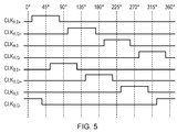
- the duty cycle of the first-TIF and second-TIF four-phase, non-overlapping clock signals is 3/16, that is, 18.75%, but the signal filter 100 is otherwise as described above with reference to Figures 1 to 4 .
- a preferred duty cycle for the first-TIF and second-TIF four-phase non-overlapping clock signals is 18.75%, the duty cycle may be in the range 16.75% to 20.75%. Waveforms of the first-TIF and second-TIF four-phase, non-overlapping clock signals having a duty cycle of 18.75% are illustrated in Figure 5 .
- each of the first-TIF first- to fourth capacitive elements C A,1 ...C A,4 is first connected in parallel with one of the second-TIF first to fourth capacitive elements C B,1 ...C B,4 from a 45 degree earlier phase for one sixteenth of the LO signal period, and then with another of the second-TIF first to fourth capacitive element C B,1 ...C B,4 from a 45 degrees later phase for one sixteenth of the clock signal period, with an intermediate interval of one sixteenth of the clock signal period in which only one of the first-TIF first to fourth capacitive elements C A,1 ...C A,4 is connected, without any of the second-TIF first to fourth capacitive elements C B,1 ...C B,4 being connected.
- a down-conversion mixer 200 comprises the signal filter 100 and is arranged for down-converting a differential input signal provided at the filter differential signal port 20.
- This differential input signal may be, for example, a radio frequency (RF) signal.
- a first differential amplifier 40 has a first non-inverting input 41 and a second inverting input 42 coupled to, respectively, the first component 30 A,1 and the third component 30 A,3 of the second signal port 30 A of the first transferred impedance filter TIF A .
- a second differential amplifier 44 has a first inverting input 45 and a second non-inverting input 46 coupled to, respectively, the first component 30 A,1 and the third component 30 A,3 of the second signal port 30 A of the first transferred impedance filter TIF A .
- a third differential amplifier 48 has a first non-inverting input 49 and a second inverting input 50 coupled to, respectively, the second component 30 A,2 and the fourth component 30 A,4 of the second signal port 30 A of the first transferred impedance filter TIF A .
- a fourth differential amplifier 52 has a first non-inverting input 53 and a second inverting input 54 coupled to, respectively, the second component 30 A,2 and the fourth component 30 A,4 of the second signal port 30 A of the first transferred impedance filter TIF A .
- a fifth differential amplifier 56 has a first non-inverting input 57 and a second inverting input 58 coupled to, respectively, the first component 30 B,1 and the third component 30 B,3 of the second signal port 30 B of the second transferred impedance filter TIF B .
- a sixth differential amplifier 60 has a first non-inverting input 61 and a second inverting input 62 coupled to, respectively, the second component 30 B,2 and the fourth component 30 A,4 of the second signal port 30 B of the second transferred impedance filter TIF B .
- the first, second, third and fourth differential amplifiers 40, 44, 48, 52 each have a first gain
- the fifth and sixth amplifiers 56, 60 have a second gain which is a multiple of the first gain.
- the multiple is in the range 1.3 to 1.6.
- the multiple is the square root of two, that is, 1.414.
- the first gain may be unity and the second gain may be 1.414, as illustrated in Figure 6 .
- the multiple is 1.5.
- the first gain may be unity and the second gain may be 1.5.
- a first summing stage 64 has a first input 65 coupled to an output 43 of the first differential amplifier 40, a second input 66 coupled to an output 51 of the third differential amplifier 48, a third input 67 coupled to an output 59 of the fifth differential amplifier 56, and an output 68 coupled to a first output 76 of the down-conversion mixer 200.
- a second summing stage 70 has a first input 71 coupled to an output 47 of the second differential amplifier 44, a second input 72 coupled to an output 55 of the fourth differential amplifier 52, a third input 73 coupled to an output 63 of the sixth differential amplifier 60, and an output 74 coupled to a second output 78 of the down-conversion mixer 200.
- the first and second summing stages 64, 70 may be implemented with passive circuitry using resistive elements coupled to a virtual ground.
- the down-conversion mixer 200 mixes down the differential input signal provided at the filter differential signal port 20 and the delivers at its first output 76 an in-phase component of the mixed down signal and delivers at its second output 78 a quadrature-phase component of the mixed down signal.
- the first to sixth differential amplifiers 40, 44, 48, 52, 56, 60 and the first and second summing stages 64, 70 together form a combining stage 120.
- a finite on resistance of the first-TIF first to eighth switch elements S A,1 ...S A,8 and of the second-TIF first to eighth switch elements S B,1 ...S B,8 may limit the available stop-band attenuation for an RF differential input signal provided at the filter differential signal port 20, but this limitation does not apply to the down-converted signal at the first and second outputs 76, 78 of the down-conversion mixer 200.
- an up-conversion mixer 300 comprises the signal filter 100 and is arranged for up-converting in-phase and quadrature-phase components I,Q of an input signal provided at, respectively, an in-phase input 80 and a quadrature-phase input 82 of the up-conversion mixer 300.
- the up-converted signal is delivered by the signal filter 100, at the filter differential signal port 20.
- the up-conversion mixer 300 also comprises a first current source 84 having a first input 85 coupled to the in-phase input 80 for receiving the in-phase component I of the input signal and a second input 86 coupled to the quadrature-phase input 82 for receiving the quadrature-phase component Q of the input signal.
- the first current source 84 is coupled between the first component 30 A,1 and the third component 30 A,3 of the second signal port 30 A of the first transferred impedance filter TIF A and is arranged to deliver a current to the signal filter 100 which is proportional to the difference, I-Q, between the in-phase component I and the quadrature-phase component Q of the input signal.
- a second current source 87 has a first input 88 coupled to the in-phase input 80 for receiving the in-phase component I of the input signal and a second input 89 coupled to the quadrature-phase input 82 for receiving the quadrature-phase component Q of the input signal.
- the second current source 87 is coupled between the second component 30 A,2 and the fourth component 30 A,4 of the second signal port 30 A of the first transferred impedance filter TIF A and is arranged to deliver a current to the signal filter 100 which is proportional to the sum, I+Q, of the in-phase component I and the quadrature-phase component Q of the input signal.
- a third current source 90 has an input 91 coupled to the in-phase input 80 for receiving the in-phase component I of the input signal and is coupled between the first component 30 B,1 and the third component 30 B,3 of the second signal port 30 B of the second transferred impedance filter TIF B and is arranged to deliver a current to the signal filter 100 which is proportional to the in-phase component I of the input signal.
- a fourth current source 92 has an input 93 coupled to the quadrature-phase input 82 for receiving the quadrature-phase component Q of the input signal and is coupled between the second component 30 B,2 and the fourth component 30 B,4 of the second signal port 30 B of the second transferred impedance filter TIF B and is arranged to deliver a current to the signal filter 100 which is proportional to the quadrature-phase component Q of the input signal.
- the first current source 84 has a gain which is equal to the current delivered to the signal filter 100 by the first current source 84 divided by the difference between in-phase component I provided at the first input 85 of the first current source 84 and the quadrature-phase component Q provided at the second input 86 of the first current source 84.
- the second current source 87 has a gain which is equal to the current delivered to the signal filter 100 by the second current source 87 divided by the sum of the in-phase component I provided at the first input 88 of the second current source 87 and the quadrature-phase component Q provided at the second input 89 of the second current source 87.
- the gain of the first current source 84 is equal to the gain of the second current source 87.
- the third current source 90 has a gain that is equal to the current delivered to the signal filter 100 by the third current source 90 divided by the in-phase component I provided at the input 91 of the third current source 90.
- the fourth current source 92 has a gain that is equal to the current delivered to the signal filter 100 by the fourth current source 92 divided by the quadrature-phase component Q provided at the input 93 of the fourth current source 92.
- the gain of the third current source 90 is equal to the gain of the fourth current source 92, and is a multiple of the gain of the first and second current sources 84, 87. This multiple is in the range 1.3 to 1.6. In one preferred embodiment, the multiple is the square root of two, that is, 1.414.
- the gain of the first and second current sources 84, 87 may be unity and the gain of the third and fourth current sources 90, 92 may be 1.414. In another preferred embodiment, the multiple is 1.5.
- the gain of the first and second current sources 84, 87 may be unity and the gain of the third and fourth current sources 90, 92 may be 1.5.
- the first, second, third and fourth current sources 84, 87, 90, 92 may be differential floating current sources, and may be implemented as current steering digital-to-analogue converters.
- the first current source 84 may determine the difference, I-Q, between the in-phase component I and the quadrature-phase component Q
- the second current source 87 may determine the sum, I+Q, of the in-phase component I and the quadrature-phase component Q, in digital domain, or by connecting separate digital-to-analogue converters for the in-phase and quadrature-phase components in parallel to drive the first-TIF first, second, third and fourth capacitive elements C A,1 , C A,2 , C A,3 , C A,4 .
- the third and fourth current sources 90, 92 may employ scaled unit current cells to provide the required gain for the currents to drive the second-TIF first, second, third and fourth capacitive elements C B1 , C B,2 , C B,3 , C B,4 .
- Harmonic rejection by the up-conversion mixer 300 suppresses undesired odd harmonics of the clock signal in the up-converted signal delivered by the signal filter 100 at the filter differential signal port 20.
- the up-conversion mixer 300 may comprise filters for band-limiting the in-phase and quadrature-phase components before they are provided to the first, second, third and fourth current sources 84, 87, 90, 92, which can also contribute to the spectral purity of the up-converted signal delivered by the signal filter 100 at the filter differential signal port 20.
- a pre-power amplifier and a power amplifier may provide more attenuation of far-off noise.
- Figure 8A illustrates differential waveforms W+, W- of the up-converted signal at RF delivered by the signal filter 100 at the filter differential signal port 20 of the up-conversion mixer 300 for the case of the first and second TIF four-phase, non-overlapping clock signals having a duty cycle of 25%
- Figure 8B illustrates the corresponding waveforms W+, W- for the case of the first and second TIF four-phase, non-overlapping clock signals having a duty cycle of 18.75%.
- no folding of the third and fifth harmonic of the clock signal occurs. Folding of the seventh and ninth harmonic of the clock signal occurs, although this is at a level 15 to 30dB lower in the case of a duty cycle of 18.75%, compared with 25%.
- Figures 8C and 8D illustrate, respectively, the corresponding waveforms for a prior art single four-path TIF and a 25% clock duty cycle and a prior art eight-path TIF with a 12.5% clock duty cycle, both of which have poorer rejection of odd harmonics of the clock signal.
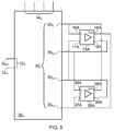
- a first transconductance amplifier 15A has a non-inverting input 16A and an inverting input 17A coupled to, respectively, the first component 30 A,1 and the third component 30 A,3 of the second signal port 30 A of the first transferred impedance filter TIF A .
- a first output 18A and a second output 19A of the first transconductance amplifier 15A are coupled to, respectively, the fourth component 30 A,4 and the second component 30 A,2 of the second signal port 30 A of the first transferred impedance filter TIF A .
- a second transconductance amplifier 35A has a non-inverting input 36A and an inverting input 37A coupled to, respectively, the second component 30 A,2 and the fourth component 30 A,4 of the second signal port 30 A of the first transferred impedance filter TIF A .
- a first output 38A and a second output 39A of the second transconductance amplifier 35A are coupled to, respectively, the first component 30 A,1 and the third component 30 A,3 of the second signal port 30 A of the first transferred impedance filter TIF A .
- the first transconductance amplifier 15A delivers to the second component of the second signal port of the first TIF 30 A,2 a first current dependent on a voltage difference at the first and third components of the second signal port of the first TIF 30 A,1 , 30 A,3 , and delivers to the fourth component of the second signal port of the first TIF 30 A,4 a second current dependent on a voltage difference at the first and third components of the second signal port of the first TIF 30 A,1 , 30 A,3 .
- the second transconductance amplifier 35A delivers to the first component of the second signal port of the first TIF 30 A,1 a third current dependent on a voltage difference at the second and fourth components of the second signal port of the first TIF 30 A,2 , 30 A,4 , and delivers to the third component of the second signal port of the first TIF 30 A,3 a fourth current dependent on a voltage difference at the second and fourth components of the second signal port of the first TIF 30 A,2 , 30 A,4 .
- a third transconductance amplifier 15B has a non-inverting input 16B and an inverting input 17B coupled to, respectively, the first component 30 B,1 and the third component 30 B,3 of the second signal port 30 B of the second transferred impedance filter TIF B .
- a first output 18B and a second output 19B of the second transconductance amplifier 1 B are coupled to, respectively, the fourth component 30 B,4 and the second component 30 B,2 of the second signal port 30 B of the second transferred impedance filter TIF B .
- a fourth transconductance amplifier 35B has a non-inverting input 36B and an inverting input 37B coupled to, respectively, the second component 30 B,2 and the fourth component 30 B,4 of the second signal port 30 B of the first transferred impedance filter TIF B .
- a first output 38B and a second output 39B of the fourth transconductance amplifier 35B are coupled to, respectively, the first component 30 B,1 and the third component 30 B,3 of the second signal port 30 B of the second transferred impedance filter TIF B .
- the third transconductance amplifier 15B delivers to the second component of the second signal port of the second TIF 30 B,2 a fifth current dependent on a voltage difference at the first and third components of the second signal port of the second TIF 30 B,1 , 30 B,3 , and delivers to the fourth component of the second signal port of the second TIF 30 B,4 a sixth current dependent on a voltage difference at the first and third components of the second signal port of the second TIF 30 B,1 , 30 B,3 .
- the fourth transconductance amplifier 35B delivers to the first component of the second signal port of the second TIF 30 B,1 a seventh current dependent on a voltage difference at the second and fourth components of the second signal port of the second TIF 30 B,2 , 30 B,4 , and delivers to the third component of the second signal port of the second TIF 30 B,3 an eighth current dependent on a voltage difference at the second and fourth components of the second signal port of the second TIF 30 B,2 , 30 B,4 .
- the first, second, third and fourth transconductance amplifiers 15A, 35A, 15B, 35B can be implemented with two simple differential stages or four simple common-source stages with minimal increase in chip area of an integrated circuit, current consumption and noise.
- Other connections between the second signal port 30 A of the first transferred impedance filter TIF A and the first to fourth differential amplifiers 40, 44, 48, 52, and between the second signal port 30 B of the second transferred impedance filter TIF B and the fifth and sixth differential amplifiers 56, 60 are unchanged, remaining the same as described above.
- the shift of centre frequency caused by parasitic capacitance can be utilised by using the down-conversion mixer 200 in a low intermediate frequency (IF) configuration rather than a zero-IF configuration.
- IF intermediate frequency
- the band-limited up-conversion with harmonic rejection, by the up-conversion mixer 300, enables a delta-sigma modulated digital-to-analogue converter to be implemented with a higher clock rate than local oscillator frequency.
- values of the ratio local oscillator frequency/clock frequency can be 1 ⁇ 2, 1, 11 ⁇ 2, 2, 21 ⁇ 2... and so on.
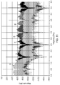
- Such a feature can be used, in particular, for a direct delta-sigma receiver which combines a continuous-time delta-sigma modulator and direct conversion receiver together with feedback from baseband to RF. This is demonstrated in Figure 11 , which illustrates the spectrum at RF of a signal after up-conversion.
- in-phase and quadrature-phase 1-bit 1GHz bit streams generated with a third order delta-sigma modulator are up-converted to 500MHz with 1-bit current digital-to-analogue converters feeding the in-phase input 80 and the quadrature-phase input 82 of the up-conversion mixer 300 with the first-TIF and second-TIF four-phase, non-overlapping clock signals having a duty cycle of 25%
- graph b) of Figure 11 illustrates the corresponding spectrum for the case of the first-TIF and second-TIF four-phase, non-overlapping clock signals having a duty cycle of 18.75%.
- a voltage controlled oscillator (VCO) signal may be divided by one divider circuit supplied with a non-inverted version of the VCO signal and another divider circuit supplied with an inverted version of the VCO signal.
- VCO voltage controlled oscillator
- An accurate 45-degree phase shift may be implemented for differential signals by using clock signal balancing buffers with single-ended duty cycle adjusting circuitry.
- a wireless transceiver 400 comprises an antenna 410 coupled to a port 462 of a duplex filter 460.
- An output 464 of the duplex filter 460 is coupled to an input of a low noise amplifier (LNA) 420.
- the filter differential port 20 of a signal filter 100 is also coupled to the input of the LNA 420.
- the signal filter 100 filters a signal received at the antenna 410.
- An output of the LNA 420 is coupled to the filter differential signal port 20 of the down-conversion mixer 200.
- the first and second outputs 76, 78 of the down-conversion mixer 200 are coupled to a baseband processor (BB) 440 for demodulating the in-phase and quadrature-phase components of a down-converted signal.
- BB baseband processor
- a phase locked loop (PLL) 430 coupled to the filter clock input 10 of the signal filter 100, and coupled to the filter clock input 10 of the signal filter 100 of the down-conversion mixer 200, generates the LO signal.
- the BB 440 is coupled to the in-phase input 80 and the quadrature-phase input 82 of the up-conversion mixer 300.
- the PLL 430 is also coupled to the filter clock input 10 of the signal filter 100 of the up-conversion mixer 300 for providing the LO signal.
- the filter differential signal port 20 of the up-conversion mixer 300 is coupled to an input of a power amplifier (PA) 450, and an output of the PA 450 is coupled to an input 466 of the duplex filter 460.
- PA power amplifier
- the wireless transceiver 400 therefore comprises a transmitter, comprising the BB 440, up-conversion mixer 300, PLL 430, PA 450, duplex filter 460 and antenna 410, and a receiver, comprising the antenna 410, duplex filter 460, filter 100, LNA 420, down-conversion mixer 200, PLL 430, and BB 440.
- the BB 440, PLL 430, duplex filter 460 and antenna 410 are shared by the transmitter and receiver.
Landscapes
- Engineering & Computer Science (AREA)
- Computer Networks & Wireless Communication (AREA)
- Signal Processing (AREA)
- Networks Using Active Elements (AREA)
Description
- The present disclosure relates to a signal filter, a down-conversion mixer comprising the signal filter, an up-conversion mixer comprising the signal filter, and a method of filtering a signal, having application in particular, but not exclusively, in wireless communication equipment for transmitting or receiving a radio frequency signal.
- A transferred impedance filter (TIF), also known as a transferred impedance filter (TIF), utilising N-path filtering techniques, such as disclosed in
US 7,187,230 and in "Tunable high-Q N-path band-pass filters: modeling and verification", A. Ghaffari et al, IEEE J. of Solid-State Circuits, May 2011, can provide narrowband bandpass filtering centred at a switching frequency, that is, a local oscillator frequency. InUS 2010/0097258 and in "A 900-MHz direct delta-sigma receiver in 65-nm CMOS", "K. Koli et al, IEEE J. of Solid-State Circuits, Dec. 2010, a direct delta-sigma receiver is disclosed employing TIFs. - A known 4-path TIF mixes a signal to a desired bandpass frequency range from odd harmonics of a local oscillator (LO) signal, using a switching duty cycle of 25%. The TIF acts as a high impedance for input frequencies close to the switching frequency, forming a high-Q bandpass filter centred at the switching frequency. A basic TIF circuit is a capacitively loaded passive mixer, and therefore it will mix signals from all odd harmonics of the LO signal. The stopband attenuation of the circuit is limited by the on-resistances of the switches employed in the TIF, and, near odd harmonics of the clock signal, additional bandpass resonances occur. The transfer function of such a 4-path TIF has repeated, but slightly attenuated, bandpass responses on every odd harmonic of the LO signal. The use of a switching duty cycle shorter than 25% can slightly improve the bandpass frequency selectivity, although attenuation at the odd harmonics of the LO signal is severely degraded, as described by Ghaffari et al.
- In order to improve the harmonic rejection capabilities, more phases than four can be used to construct 6 or 8-path TIFs, as disclosed by Ghaffri et al. For example, mixing down from odd harmonics of the LO signal can be reduced by using, for example, an 8-path TIF with a 12.5% switching duty cycle. That, however, leads to reduced attenuation at harmonics of the clock signal, rendering the benefits of the circuit rather limited, while significantly increasing the maximum VCO frequency required for generating the LO signal. The main reason for the reduced attenuation is the shorter switch on-time, which limits the filtering at odd harmonics of the LO signal, while slightly reducing losses in the desired passband. The TIF is usually connected in parallel with a passive LC-resonator, which reduces the losses in the TIF passband, although this is insignificant compared with the losses of the passive LC-resonator. Furthermore, the harmonic rejection capabilities of the LC-resonator alone are not enough for typical applications, for example for wireless local area network (WLAN) coexistence in cellular transceivers.
- Therefore, there is a requirement for improved filtering.
-
EP 2204907 discloses a four-phase TIF driven by LO signals having a duty cycle of about 20%, or less than 25%, and an eight-phase TIF driven by LO signals having a duty cycle of about 12.5% or less. - According to a first aspect, there is provided a signal filter comprising:
- a first transferred impedance filter, TIF, having:
- a first differential signal port of the first-TI F having a first component and a second component;
- a second signal port of the first TIF having a first component, a second component, a third component and a fourth component;
- first-TIF first, second, third and fourth capacitive elements coupled between a ground and, respectively, the first component, the second component, the third component and the fourth component of the second signal port of the first TIF; and
- first, second, third and fourth first-TIF differential signal paths, each of the first-TIF differential signal paths having a respective first component path and a respective second component path;
- wherein
- the first component paths of the first, second, third and fourth first-TIF differential signal paths are arranged between the first component of the first differential signal port of the first TIF and, respectively, the first component, the second component, the third component and the fourth component of the second signal port of the first TIF, and are selectable by means of, respectively, first-TIF first, second, third and fourth switch elements; and
- the second component paths of the first, second, third and fourth first-TI F differential signal paths are arranged between the second component of the first differential signal port of the first TIF and, respectively, the third, fourth, first and second components of the second signal port of the first TIF, and are selectable by means of, respectively, first-TIF fifth, sixth, seventh, and eighth switch elements;
- a second transferred impedance filter, TIF, having:
- a first differential signal port of the second TIF having a first component and a second component, and being coupled to the first differential signal port of the first TIF;
- a second signal port of the second TIF having a first component, a second component, a third component and a fourth component;
- second-TIF first, second, third and fourth capacitive elements coupled between the ground and, respectively the first component, the second component, the third component and the fourth component of the second signal port of the second TIF; and
- first, second, third and fourth second-TIF differential signal paths, each of the first, second, third and fourth second-TIF differential signal paths having a respective first component path and a respective second component path;
- wherein
- the first component paths of the first, second, third and fourth second-TIF differential signal paths are arranged between the first component of the first differential signal port of the second TIF and, respectively, the first component, the second component, the third component and the fourth component of the second signal port of the second TIF, and are selectable by means of, respectively, second-TIF first, second, third and fourth switch elements;
- the second component paths of the first, second, third and fourth second-TIF differential signal paths are arranged between the second component of the first differential signal port of the second TIF and, respectively, the third, fourth, first and second components of the second signal port of the second TIF, and are selectable by means of, respectively, second-TIF fifth, sixth, seventh, and eighth switch elements;
- a first clock generator arranged to provide first-TIF first, second, third and fourth clock signals having non-overlapping phases for selecting, respectively, the first, second, third and fourth first-TIF differential signal paths; and
- a second clock generator arranged to provide second-TIF first, second, third and fourth clock signals having non-overlapping phases for selecting, respectively, the first, second, third and fourth second-TIF differential signal paths;
- wherein the phases of the second-TIF first, second, third and fourth clock signals are equal to the phases of, respectively, the first-TIF first, second, third and fourth clock signals delayed by 45 degrees;
- According to a second aspect, there is provided a method of filtering a signal using a first 4-differential-path transferred impedance filter, TIF, having:
- a first differential signal port of the first-TIF having a first component and a second component;
- a second signal port of the first TIF having a first component, a second component, a third component and a fourth component;
- first-TIF first, second, third and fourth capacitive elements coupled between a ground and, respectively, the first component, the second component, the third component and the fourth component of the second signal port of the first TIF; and
- first, second, third and fourth first-TIF differential signal paths, each of the first-TIF differential signal paths having a respective first component path and a respective second component path;
- wherein
- the first component paths of the first, second, third and fourth first-TIF differential signal paths are arranged between the first component of the first differential signal port of the first TIF and, respectively, the first component, the second component, the third component and the fourth component of the second signal port of the first TIF, and are selectable by means of, respectively, first-TIF first, second, third and fourth switch elements; and
- the second component paths of the first, second, third and fourth first-TIF differential signal paths are arranged between the second component of the first differential signal port of the first TIF and, respectively, the third, fourth, first and second components of the second signal port of the first TIF, and are selectable by means of, respectively, first-TIF fifth, sixth, seventh, and eighth switch element;
and- a second 4-differential-path transferred impedance filter having:
- a first differential signal port of the second TIF having a first component and a second component, and being coupled to the first differential signal port of the first TIF;
- a second signal port of the second TIF having a first component, a second component, a third component and a fourth component;
- second-TIF first, second, third and fourth capacitive elements coupled between the ground and, respectively the first component, the second component, the third component and the fourth component of the second signal port of the second TIF; and
- first, second, third and fourth second-TIF differential signal paths, each of the first, second, third and fourth second-TIF differential signal paths having a respective first component path and a respective second component path
- wherein
- the first component paths of the first, second, third and fourth second-TIF differential signal paths are arranged between the first component of the first differential signal port of the second TIF and, respectively, the first component, the second component, the third component and the fourth component of the second signal port of the second TIF, and are selectable by means of, respectively, second-TIF first, second, third and fourth switch elements;
- the second component paths of the first, second, third and fourth second-TIF differential signal paths are arranged between the second component of the first differential signal port of the second TIF and, respectively, the third, fourth, first and second components of the second signal port of the second TIF, and are selectable by means of, respectively, second-TIF fifth, sixth, seventh, and eighth switch elements; the method comprising:
- selecting respective differential signal paths of the first 4-differential-path transferred impedance filter with first-TIF clock signals having four non-overlapping phases; and
- selecting respective differential signal paths; of the second 4-differential-path transferred impedance filter with second-TI F clock signals having four non-overlapping phases;
- wherein the phases of the second-TIF clock signals are equal to the phases of the first-TIF clock signals delayed by 45 degrees;
- a second 4-differential-path transferred impedance filter having:
- Therefore, the signal filter may comprise two 4-differential-path TIFs coupled in parallel. Each of the TIFs may be clocked with clock signals having four non-overlapping phases and a duty cycle in the range 16.75% to 25%, the phases of the clock signals used for clocking the second TIF being delayed by 45 degrees with respect to the phases of the clock signals used for clocking the first TIF. The signal filter and the method of filtering a signal can enable reduced harmonic folding, higher attenuation around odd harmonics of the frequency of the clock signals and reduced sensitivity to phase errors in the clock signals, without requiring an increased oscillator frequency for generating the clock signals. The use of differential signal paths can provide rejection of all even harmonics. Such a signal filter and method of filtering a signal may be used for radio frequency (RF) narrowband bandpass filtering without inductors, and have application, for example, in low
- band cellular or digital television receivers where integrated inductors have previously required intolerably large silicon areas in an integrated circuit.
- In one embodiment, the first-TIF first, second, third and fourth clock signals and the second-TIF first, second, third and fourth clock signals may have a duty cycle in the
range 20 to 25%, and preferably 25%, that is, a quarter. This can reduce folding from third, fifth, eleventh, thirteen and nineteenth harmonics of the frequency of the clock signal. - In another embodiment, the first-TIF first, second, third and fourth clock signals and the second-TIF first, second, third and fourth clock signals may have a duty cycle in the range 16.75 to 20.75%, and preferably 18.75%, that is, three sixteenths. This can enable reduced folding from seventh, ninth, fifteenth and seventeenth order harmonics of the frequency of the clock signal, for example by 15 to 30dB.
- The first and second TIFs can have an identical structure, which can simplify integrated circuit design, manufacture and testing.
- The signal filter may comprise a first transconductance amplifier arranged to deliver to the second component of the second signal port of the first TIF a first current dependent on a voltage difference at the first and third components of the second signal port of the first TIF, and to deliver to the fourth component of the second signal port of the first TIF a second current dependent on a voltage difference at the first and third components of the second signal port of the first TIF; a second transconductance amplifier arranged to deliver to the first component of the second signal port of the first TIF a third current dependent on a voltage difference at the second and fourth components of the second signal port of the first TIF, and to deliver to the third component of the second signal port of the first TIF a fourth current dependent on a voltage difference at the second and fourth components of the second signal port of the first TIF; a third transconductance amplifier arranged to deliver to the second component of the second signal port of the second TIF a fifth current dependent on a voltage difference at the first and third components of the second signal port of the second TIF, and to deliver to the fourth component of the second signal port of the second TIF a sixth current dependent on a voltage difference at the first and third components of the second signal port of the second TIF; and a fourth transconductance amplifier arranged to deliver to the first component of the second signal port of the second TIF a seventh current dependent on a voltage difference at the second and fourth components of the second signal port of the second TIF, and to deliver to the third component of the second signal port of the second TIF an eighth current dependent on a voltage difference at the second and fourth components of the second signal port of the second TIF. This feature can provide compensation for a shift in centre frequency of bandpass filtering, caused by parasitic capacitance.
- A down-conversion mixer may comprise the signal filter for down-converting an input signal applied to the first differential signal port of the first TIF and to the first differential signal port of the second, and further comprising a combining stage arranged to provide: at a first output of the down-conversion mixer the sum of voltages at the first and second components of the second signal port of the first TIF times a first gain and a voltage at the first component of the second signal port of the second TIF times a second gain, minus voltages at the third and fourth components of the second signal port of the first TIF times the first gain and a voltage at the third component of the second signal port of the second TIF times the second gain; and at a second output of the down-conversion mixer the sum of voltages at the second and third components of the second signal port of the first TIF times the first gain and a voltage at the second component of the second signal port of the second TIF times the second gain, minus voltages at the first and fourth components of the second signal port of the first TIF times the first gain and a voltage at the fourth component of the second signal port of the second TIF times the second gain; wherein the second gain is in the range 1.3 to 1.6 times the first gain.
- Therefore, a down-conversion mixer can be provided having the advantages described above for the signal filter. Such a range of ratios between the first and second gains enables good harmonic rejection. The first gain may be unity.
- Such a down-conversion mixer comprising the signal filter, for down-converting an input signal applied to the first differential signal port of the first TIF and to the first differential signal port of the second TIF, may comprise:
- a first differential amplifier having a first non-inverting input coupled to the first component of the second signal port of the first TIF and a second inverting input coupled to the third component of the second signal port of the first TIF;
- a second differential amplifier having a first inverting input coupled to the first component of the second signal port of the first TIF and a second non-inverting input coupled to the third component of the second signal port of the first TIF;
- a third differential amplifier having a first non-inverting input coupled to the second component of the second signal port of the first TIF and a second inverting input coupled to the fourth component of the second signal port of the first TIF;
- a fourth differential amplifier having a first non-inverting input coupled to the second component of the second signal port of the first TIF and a second inverting input coupled to the fourth component of the second signal port of the first TIF;
- a fifth differential amplifier having a first non-inverting input coupled to the first component of the second signal port of the second TIF and a second inverting input coupled to the third component of the second signal port of the second TIF;
- a sixth differential amplifier having a first non-inverting input coupled to the second component of the second signal port of the second TIF and a second inverting input coupled to the fourth component of the second signal port of the second TIF;
- a first summing stage having a first input coupled to an output of the first differential amplifier, a second input coupled to an output of the third differential amplifier, a third input coupled to an output of the fifth differential amplifier, and an output coupled to a first output of the down-conversion mixer;
- a second summing stage having a first input coupled to an output of the second differential amplifier, a second input coupled to an output of the fourth differential amplifier, a third input coupled to an output of the sixth differential amplifier, and an output coupled to a second output of the down-conversion mixer;
- wherein the first, second, third and fourth differential amplifiers have a first gain and the fifth and sixth amplifiers have a second gain in the range 1.3 to 1.6 times the first gain. At least one of the first and second summing stages may comprise only resistors.
- The second gain may be equal to the first gain times 1.5. Such a ratio between the first and second gain can enable improved harmonic rejection.
- The second gain may be equal to the first gain times the square root of two. Such a ratio between the first and second gain can enable further improved harmonic rejection.
- An up-conversion mixer comprising the signal filter, for up-converting an input signal comprising an in-phase component and a quadrature-phase component, may further comprise:
- a first differential current source coupled to the first and third components of the second port of the first TIF for providing a first drive current equal to the difference between the in-phase and quadrature-phase components of the input signal times a first constant;
- a second differential current source coupled to the second and fourth components of the second port of the first TIF for providing a second drive current equal to the sum of the in-phase and quadrature-phase components of the input signal times the first constant;
- a third differential current source coupled to the first and third components of the second port of the second TIF for providing a third drive current in the range 1.3 to 1.6 times the in-phase component times the first constant;
- a fourth differential current source coupled to the second and fourth components of the second port of the second TIF for providing a fourth drive current in the range 1.3 to 1.6 times the quadrature-phase component times the first constant.
- Therefore, an up-conversion mixer can be provided having the advantages described above for the signal filter. Such a range of ratios between the third drive current and the in-phase component, and between the fourth drive current and the quadrature-phase component, enables good harmonic rejection. The first constant may be unity.
- The third drive current may be equal to the in-phase component times the first constant times 1.5, and the fourth drive current may be equal to the quadrature-phase component times the first constant times 1.5. Such a ratio between the third drive current and the in-phase component, and between the fourth drive current and the quadrature-phase component, can enable improved harmonic rejection.
- Alternatively, the third drive current may be equal to the in-phase component times the first constant times the square root of two, and the fourth drive current may be equal to the quadrature-phase component times the first constant times the square root of two. Such a ratio between the third drive current and the in-phase component, and between the fourth drive current and the quadrature-phase component, can enable further improved harmonic rejection.
- There is also provided a wireless communication apparatus, for example a transmitter, receiver or transceiver, comprising the signal filter.
- Preferred embodiments will now be described, by way of example only, with reference to the accompanying drawings, in which:
-
Figure 1 is a schematic diagram of a signal filter; -
Figure 2 illustrates waveforms of clock signals of the signal filter; -
Figure 3 illustrates a first transferred impedance filter; -
Figure 4 illustrates a second transferred impedance filter; -
Figure 5 illustrates waveforms of clock signals of another embodiment of the signal filter; -
Figure 6 is a schematic diagram of a down-conversion mixer; -
Figure 7 is a schematic diagram of an up-conversion mixer; -
Figures 8A to 8D illustrate waveforms of an up-converted signal; -
Figure 9 is a schematic diagram of a first TIF with capacitance compensation; -
Figure 10 is a schematic diagram of a second TIF with capacitance compensation; -
Figure 11 illustrates RF spectra of an up-converted signal; and -
Figure 12 is a block diagram of a wireless transceiver. - Referring to
Figure 1 , asignal filter 100 has a filterdifferential signal port 20 comprising first andsecond components 20+, 20-. The first andsecond components 20+, 20- of the filterdifferential signal port 20 are coupled to respective first and second components 32A+, 32A- of a first differential signal port 32A of a first transferred impedance filter TIFA and to respective first and second components 32B+, 32B- of a first differential signal port 32B of a second transferred impedance filter TIFB. In this way, the first differential signal port 32A of the first transferred impedance filter TIFA and the first differential signal port 32B of the second transferred impedance filter TIFB are coupled together, the first transferred impedance filter TIFA and the second transferred impedance filter TIFB therefore being coupled in parallel. The first transferred impedance filter TIFA has a second signal port 30A comprising first, second, third and fourth components 30A,1, 30A,2, 30A,3, 30A,4, and the second transferred impedance filter TIFB has a second signal port 30B comprising first, second third and fourth components 30B,1, 30B,2, 30B,3, 30B,4. The first and second transferred impedance filters TIFA, TIFB are four-differential-path transferred impedance filters, that is, each of the first and second transferred impedance filters TIFA, TIFB provides four paths for a differential signal between their respective first differential signal ports 32A, 32B and their respective second signal ports 30A, 30B. - A
filter clock input 10 for a clock signal, also referred to as a local oscillator (LO) signal, is coupled to a first clock generator 12A and to a second clock generator 12B. The first clock generator 12A generates first-TIF four-phase, non-overlapping clock signals comprising a first-TIF first-phase clock signal CLKA,I+ having a duty cycle of 25%, a first-TIF second-phase clock signal CLKA,Q, having a phase equal to the phase of the first-TIF first-phase clock signal CLKA,I+ delayed by 90 degrees, a first-TIF third-phase clock signal CLKA,I- having a phase equal to the phase of the first-TIF second-phase clock signal CLKA,Q+ delayed by 90 degrees, and a first-TIF fourth-phase clock signal CLKA,Q- having a phase equal to the phase of the first-TIF third-phase clock signal CLKA,I+ delayed by 90 degrees. The first clock generator 12A may generate the first-TIF four-phase, non-overlapping clock signals using a divide-by-four circuit, The first clock generator 12A is coupled to a first clock port 34A of the first transferred impedance filter TIFA for delivering the first-TIF four-phase, non-overlapping clock signals. - The second clock generator 12B generator comprises a
phase shift circuit 14 for generating a delayed LO signal, and aclock circuit 13 coupled to thephase shift circuit 14 for generating second-TIF four-phase, non-overlapping clock signals comprising a second-TIF first-phase clock signal CLKB,I+ having a duty cycle of 25%, a second-TIF first-phase clock signal CKB,Q+ having a phase equal to the phase of the second-TIF first-phase clock signal CLKB,I+ delayed by 90 degrees, a second-TIF third-phase clock signal CLKB,I-having a phase equal to the phase of the second-TIF second-phase clock signal CLKB,Q+ delayed by 90 degrees, and a second-TIF fourth-phase clock signal CLKB,Q- having a phase equal to the phase of the second-TIF third-phase clock signal CLKB,I+ delayed by 90 degrees. The phase shift introduced by thephase shift circuit 14 is 45 degrees, that is, one eighth of the period of the LO signal. Therefore, the second-TIF four-phase, non-overlapping clock signals are equal in phase to the first-TIF four-phase, non-overlapping clock signals delayed by 45 degrees. The 45-degree time shift may be implemented in thephase shift circuit 14 by inverting the LO signal. For best accuracy of the phase shift, the LO signal can be a differential signal. Waveforms of the first-TIF and second-TIF four-phase, non-overlapping clock signals are illustrated inFigure 2 . Theclock circuit 13 may be a copy of the first clock generator 12A. The second clock generator 12B is coupled to a second clock port 34B of the second transferred impedance filter TIFB for delivering the second-TIF four-phase, non-overlapping clock signals. Although a preferred duty cycle for the first-TIF and second-TIF four-phase non-overlapping clock signals is 25%, the duty cycle may be in therange 20% to 25%. - Referring to
Figure 3 , the first transferred impedance filter TIFA comprises first, second, third and fourth differential signal paths PA,1, PA,2,, PA,3, PA,4 between the first differential signal port 32A of the first transferred impedance filter TIFA and the second signal port 30A of the first transferred impedance filter TIFA, each of these differential signal paths comprising a first component and a second component. - In more detail, first component paths of the first, second, third and fourth first-TIF differential signal paths PA,1+, PA,2+, PA,3+, PA,4+ are provided between the first component of the first differential signal port of the first TIF 32A+ and, respectively, the first, second, third and fourth components of the second signal port of the first TIF 30A,1, 30A,2, 30A,3, 30A,4. Second component paths of the first, second, third and fourth first-TIF differential signal paths PA,1-, PA,2-, PA,3-, PA,4- are provided between the second component of the first differential signal port of the first TIF 32A- and, respectively, the third, fourth, first and second components of the second signal port of the first TIF 30A,3, 30A,4, 30A,1, 30A,2.
- The first component paths of the first, second, third and fourth first-TIF differential signal paths PA,1+, PA,2+, PA,3+, PA,4+ are selectable by means of, respectively, first-TIF first, second, third and fourth switch elements SA,1, SA,2, SA,3, SA,4 which are coupled in the respective paths, under the control of the first-TIF four-phase, non-overlapping clock signals, and the second component paths of the first, second, third and fourth first-TIF differential signal paths PA,1-, PA,2-, PA,3-, PA,4- are selectable by means of, respectively, first-TIF fifth, sixth, seventh, and eighth switch elements SA,5, SA,6, SA,7, SA,8 which are coupled in the respective paths, under the control of the first-TIF four-phase, non-overlapping clock signals. In particular, the first-TIF first-phase clock signal CLKA,I+ controls the closure of the first-TIF first and fifth switch elements SA,1, SA,5 in, respectively, the first and second component paths of the first first-TIF differential signal path PA,1+, PA,1. The first-TIF second-phase clock signal CLKA,Q+ controls the closure of the first-TIF second and sixth switch elements SA,2, SA,6 in, respectively, the first and second component paths of the second first-TIF differential signal path PA,2+, PA,2-. The first-TIF third-phase clock signal CLKA,I- controls the closure of the first-TIF third and seventh switch elements SA,3, SA,7 in, respectively, the first and second component paths of the third first-TIF differential signal path PA,3+, PA,3-. The first-TIF fourth-phase clock signal CLKA,Q- controls the closure of the first-TIF fourth and eighth switch elements SA,4, SA,8 in, respectively, the first and second component paths of the fourth first-TIF differential signal path PA,4+, PA,4-.
- The first transferred impedance filter TIFA also comprises first-TIF first, second, third and fourth capacitive elements CA,1, CA,2, CA,3, CA,4 coupled between a ground and respective ones of the first, second, third and fourth components 30A,1, 30A,2, 30A,3, 30A,4 of the second signal port 30A of the first transferred impedance filter TIFA. Therefore, by operation of the first-TIF first to eighth switch elements SA,1...SA,8, two of the first-TIF first to fourth capacitive elements CA,1... CA,4 are coupled to the first and
second components 20+, 20- of the filterdifferential signal port 20 throughout operation of thesignal filter 100, except for any relatively short periods of non-overlap during periods of changeover between the first TIF four-phase, non-overlapping clock signals. - Likewise, referring to
Figure 4 , the structure of the second transferred impedance filter TIFB is identical to the structure of the first transferred impedance filter TIFA. The second transferred impedance filter TIFB comprises first, second, third and fourth differential signal paths PB,1, PB,2,, PB,3, PB,4 between the first differential signal port 32B of the second transferred impedance filter TIFB and the second signal port 30B of the second transferred impedance filter TIFB, each of these differential signal paths comprising a first component and a second component. - In more detail, first component paths of the first, second, third and fourth second-TIF differential signal paths PB,1+, PB,2+, PB,3+, PB,4+ are provided between the first component of the first differential signal port of the second TIF 32B+ and, respectively, the first, second, third and fourth components of the second signal port of the second TIF 30B,1, 30B,2, 30B,3, 30B,4. Second component paths of the first, second, third and fourth second-TIF differential signal paths PB,1-, PB,2-, PB,3-, PB,4- are provided between the second component of the first differential signal port of the second TIF 32B- and, respectively, the third, fourth, first and second components of the second signal port of the second TIF 30B,3, 30B,4, 30B,1, 30B,2.
- The first component paths of the first, second, third and fourth second-TIF differential signal paths PB,1+, PB,2+, PB,3+, PB,4+ are selectable by means of, respectively, second-TIF first, second, third and fourth switch elements SB,1, SB,2, SB,3, SB,4 which are coupled in the respective paths, under the control of the second-TIF four-phase, non-overlapping clock signals, and the second component paths of the first, second, third and fourth second-TIF differential signal paths PB,1-, PB,2-, PB,3-, PB,4- are selectable by means of, respectively, second-TIF fifth, sixth, seventh, and eighth switch elements SB,5, SB,6, SB,7, SB,8 which are coupled in the respective paths, under the control of the second-TIF four-phase, non-overlapping clock signals. In particular, the second-TIF first-phase clock signal CLKB,I+ controls the closure of the second-TIF first and fifth switch elements SB,1, SB,5 in, respectively, the first and second component paths of the first second-TIF differential signal path PB,1+, PB,1-. The second-TIF second-phase clock signal CLKB,Q+ controls the closure of the second-TIF second and sixth switch elements SB,2, SB,6 in, respectively, the first and second component paths of the second second-TIF differential signal path PB,2+, PB,2-. The second-TIF third-phase clock signal CLKB,I- controls the closure of the second-TIF third and seventh switch elements SB,3, SB,7 in, respectively, the first and second component paths of the third second-TIF differential signal path PB,3+, PB,3-. The second-TIF four-phase clock signal CLKB,Q- controls the closure of the second-TIF fourth and eighth switch elements SB,4, SB,8 in, respectively, the first and second component paths of the fourth second-TIF differential signal path PB,4+, PB,4-.
- The second transferred impedance filter TIFB also comprises second-TIF first, second, third and fourth capacitive elements CB,1, CB,2, CB,3, CB,4 coupled between a ground and respective ones of the first, second, third and fourth components 30B,1, 30B,2, 30B,3, 30B,4 of the second signal port of the second transferred impedance filter TIFB. Therefore, by operation of the first to eighth switch elements SB,1...SB,8 of the second transferred impedance filter TIFB, two of the second TIF first to fourth capacitive elements CB,1... CB,4 are coupled to the first and
second components 20+, 20- of the filterdifferential signal port 20 throughout operation of thesignal filter 100, except for any relatively short periods of non-overlap during periods of changeover between the second TIF four-phase, non-overlapping clock signals. The first-TIF first, second, third and fourth capacitive elements CA,1, CA,2, CA,3, CA,4 and the second-TIF first, second, third and fourth capacitive elements CB,1, CB,2, CB,3, CB,4 have equal capacitance values, although some mismatch can be acceptable. - Referring again to
Figure 2 , during the period 0° to 45°, by operation of, that is, in response to, the first-TIF first-phase clock signal CLKA,I+, the first-TIF first capacitive element CA,1 is coupled to thefirst component 20+ of the filterdifferential signal port 20, and the first-TIF third capacitive element CA,3 is coupled to the second component 20- of the filterdifferential signal port 20. Also during the period 0° to 45°, by operation of the second-TIF fourth-phase clock signal CLKB,Q-, the second-TIF fourth capacitive element CB,4 is coupled to thefirst component 20+ of the filterdifferential signal port 20, and the second-TIF second capacitive element CA,2 is coupled to the second component 20- of the filterdifferential signal port 20. - During the
period 45° to 90°, by operation of the first-TIF first-phase clock signal CLKA,I+, the first-TIF first capacitive element CA,1 remains coupled to thefirst component 20+ of the filterdifferential signal port 20, and the first-TIF third capacitive element CA,3 remains coupled to the second component 20- of the filterdifferential signal port 20. Also during theperiod 45° to 90°, by operation of the second-TIF first-phase clock signal CLKB,I+, the second-TIF first capacitive element CB,1 is coupled to thefirst component 20+ of the filterdifferential signal port 20, and the second-TIF third capacitive element CB,3 is coupled to the second component 20- of the filterdifferential signal port 20. - During the
period 90° to 135°, by operation of the first-TIF second-phase clock signal CLKA,Q+, the first-TIF second capacitive element CA,2 is coupled to thefirst component 20+ of the filterdifferential signal port 20, and the first-TIF fourth capacitive element CA,4 is coupled to the second component 20- of the filterdifferential signal port 20. Also during theperiod 90° to 135°, by operation of the second-TIF first-phase clock signal CLKB,I+, the second-TIF first capacitive element CB,1 remains coupled to thefirst component 20+ of the filterdifferential signal port 20, and the second-TIF third capacitive element CB,3 remains coupled to the second component 20- of the filterdifferential signal port 20. - During the period 135° to 180°, by operation of the first-TIF second-phase clock signal CLKA,Q+, the first-TIF second capacitive element CA,2 remains coupled to the
first component 20+ of the filterdifferential signal port 20, and the first-TIF fourth capacitive element CA,4 remains coupled to the second component 20- of the filterdifferential signal port 20. Also during the period 135° to 180°, by operation of the second-TIF second-phase clock signal CLKB,Q+, the second-TIF second capacitive element CB,2 is coupled to thefirst component 20+ of the filterdifferential signal port 20, and the second-TIF fourth capacitive element CB,4 is coupled to the second component 20- of the filterdifferential signal port 20. - During the period 180° to 225°, by operation of the first-TIF third-phase clock signal CLKA,I-, the first-TIF third capacitive element CA,3 is coupled to the
first component 20+ of the filterdifferential signal port 20, and the first-TIF first capacitive element CA,1 is coupled to the second component 20- of the filterdifferential signal port 20. Also during the period 180° to 225°, by operation of the second-TIF second-phase clock signal CLKB,Q+, the second-TIF second capacitive element CB,2 remains coupled to thefirst component 20+ of the filterdifferential signal port 20, and the second-TIF fourth capacitive element CB,4 remains coupled to the second component 20- of the filterdifferential signal port 20. - During the period 225° to 270°, by operation of the first-TIF third-phase clock signal CLKA,I-, the first-TIF third capacitive element CA,3 remains coupled to the
first component 20+ of the filterdifferential signal port 20, and the first-TIF first capacitive element CA,1 remains coupled to the second component 20- of the filterdifferential signal port 20. Also during the period 225° to 270°, by operation of the second-TIF third-phase clock signal CLKB,I-, the second-TIF third capacitive element CB,3 is coupled to thefirst component 20+ of the filterdifferential signal port 20, and the second-TIF first capacitive element CB,1 is coupled to the second component 20- of the filterdifferential signal port 20. - During the period 270° to 315°, by operation of the first-TIF fourth-phase clock signal CLKA,Q-, the first-TIF fourth capacitive element CA,4 is coupled to the
first component 20+ of the filterdifferential signal port 20, and the first-TIF second capacitive element CA,2 is coupled to the second component 20- of the filterdifferential signal port 20. Also during the period 270° to 315°, by operation of the second-TIF third-phase clock signal CLKB,I-, the second-TIF third capacitive element CB,3 remains coupled to thefirst component 20+ of the filterdifferential signal port 20, and the second-TIF first capacitive element CB,1 remains coupled to the second component 20- of the filterdifferential signal port 20. - During the period 315° to 360°, by operation of the first-TIF fourth-phase clock signal CLKA,Q-, the first-TIF fourth capacitive element CA,4 remains coupled to the
first component 20+ of the filterdifferential signal port 20, and the first-TIF second capacitive element CA,2 remains coupled to the second component 20- of the filterdifferential signal port 20. Also during the period 315° to 360°, by operation of the second-TIF fourth-phase clock signal CLKB,Q-, the second-TIF fourth capacitive element CB,4 is coupled to thefirst component 20+ of the filterdifferential signal port 20, and the second-TIF second capacitive element CB,2 is coupled to the second component 20- of the filterdifferential signal port 20. - Therefore, with this switch timing, each first-TIF first to fourth capacitive elements CA,1...CA,4 is first connected in parallel with one of the second-TIF first to fourth capacitive elements CB,1...CB,4 from a 45 degree earlier phase for one eighth of the LO signal period, and then with another of the second-TIF first to fourth capacitive element CB,1... CB,4 from a 45 degrees later phase for one eighth of the LO signal period. With an ideal 45-degree phase difference, no folding from the third and fifth harmonics of the clock signal frequency will occur, while the seventh and ninth harmonics are folded.
- In a variation of the
signal filter 100, the duty cycle of the first-TIF and second-TIF four-phase, non-overlapping clock signals is 3/16, that is, 18.75%, but thesignal filter 100 is otherwise as described above with reference toFigures 1 to 4 . Although a preferred duty cycle for the first-TIF and second-TIF four-phase non-overlapping clock signals is 18.75%, the duty cycle may be in the range 16.75% to 20.75%. Waveforms of the first-TIF and second-TIF four-phase, non-overlapping clock signals having a duty cycle of 18.75% are illustrated inFigure 5 . In this case, there is a period of 22.5 degrees, that is, one sixteenth of a clock signal period between the end of each of the four-phase non-overlapping clock signals and the start of the next one of those phases. Moreover, each of the first-TIF first- to fourth capacitive elements CA,1...CA,4 is first connected in parallel with one of the second-TIF first to fourth capacitive elements CB,1...CB,4 from a 45 degree earlier phase for one sixteenth of the LO signal period, and then with another of the second-TIF first to fourth capacitive element CB,1...CB,4 from a 45 degrees later phase for one sixteenth of the clock signal period, with an intermediate interval of one sixteenth of the clock signal period in which only one of the first-TIF first to fourth capacitive elements CA,1...CA,4 is connected, without any of the second-TIF first to fourth capacitive elements CB,1...CB,4 being connected. Therefore, the non-overlap time and each overlap time is equal. This condition is met with a duty cycle of 3/16 if the non-zero rise and fall times of the signals are neglected. With an ideal 45 degree phase difference between the first-TIF four-phase, non-overlapping clock signals and the second-TIF four-phase, non-overlapping clock signals, no folding from third and fifth harmonic of the clock signal frequency occurs, while the seventh and ninth harmonic are folded, but at a 15 to 30dB lower level. - Therefore, with either the 25% or 18.75% duty cycle, less folding from all harmonics of the clock signal frequency occurs than with single 4-path or 8-path differential TIF.
- Referring to
Figure 6 , a down-conversion mixer 200 comprises thesignal filter 100 and is arranged for down-converting a differential input signal provided at the filterdifferential signal port 20. This differential input signal may be, for example, a radio frequency (RF) signal. A firstdifferential amplifier 40 has a firstnon-inverting input 41 and asecond inverting input 42 coupled to, respectively, the first component 30A,1 and the third component 30A,3 of the second signal port 30A of the first transferred impedance filter TIFA. A seconddifferential amplifier 44 has afirst inverting input 45 and a secondnon-inverting input 46 coupled to, respectively, the first component 30A,1 and the third component 30A,3 of the second signal port 30A of the first transferred impedance filter TIFA. A thirddifferential amplifier 48 has a firstnon-inverting input 49 and asecond inverting input 50 coupled to, respectively, the second component 30A,2 and the fourth component 30A,4 of the second signal port 30A of the first transferred impedance filter TIFA. A fourthdifferential amplifier 52 has a firstnon-inverting input 53 and asecond inverting input 54 coupled to, respectively, the second component 30A,2 and the fourth component 30A,4 of the second signal port 30A of the first transferred impedance filter TIFA. A fifthdifferential amplifier 56 has a firstnon-inverting input 57 and asecond inverting input 58 coupled to, respectively, the first component 30B,1 and the third component 30B,3 of the second signal port 30B of the second transferred impedance filter TIFB. A sixthdifferential amplifier 60 has a firstnon-inverting input 61 and asecond inverting input 62 coupled to, respectively, the second component 30B,2 and the fourth component 30A,4 of the second signal port 30B of the second transferred impedance filter TIFB. - The first, second, third and fourth
differential amplifiers sixth amplifiers Figure 6 . In another preferred embodiment, the multiple is 1.5. For example, the first gain may be unity and the second gain may be 1.5. - A first summing
stage 64 has afirst input 65 coupled to anoutput 43 of the firstdifferential amplifier 40, asecond input 66 coupled to anoutput 51 of the thirddifferential amplifier 48, athird input 67 coupled to anoutput 59 of the fifthdifferential amplifier 56, and anoutput 68 coupled to afirst output 76 of the down-conversion mixer 200. A second summingstage 70 has afirst input 71 coupled to anoutput 47 of the seconddifferential amplifier 44, asecond input 72 coupled to anoutput 55 of the fourthdifferential amplifier 52, athird input 73 coupled to anoutput 63 of the sixthdifferential amplifier 60, and anoutput 74 coupled to asecond output 78 of the down-conversion mixer 200. The first and second summingstages conversion mixer 200 mixes down the differential input signal provided at the filterdifferential signal port 20 and the delivers at itsfirst output 76 an in-phase component of the mixed down signal and delivers at its second output 78 a quadrature-phase component of the mixed down signal. The first to sixthdifferential amplifiers stages stage 120. - In the down-
conversion mixer 200, a finite on resistance of the first-TIF first to eighth switch elements SA,1...SA,8 and of the second-TIF first to eighth switch elements SB,1...SB,8 may limit the available stop-band attenuation for an RF differential input signal provided at the filterdifferential signal port 20, but this limitation does not apply to the down-converted signal at the first andsecond outputs conversion mixer 200. - Referring to
Figure 7 , an up-conversion mixer 300 comprises thesignal filter 100 and is arranged for up-converting in-phase and quadrature-phase components I,Q of an input signal provided at, respectively, an in-phase input 80 and a quadrature-phase input 82 of the up-conversion mixer 300. The up-converted signal is delivered by thesignal filter 100, at the filterdifferential signal port 20. The up-conversion mixer 300 also comprises a firstcurrent source 84 having afirst input 85 coupled to the in-phase input 80 for receiving the in-phase component I of the input signal and asecond input 86 coupled to the quadrature-phase input 82 for receiving the quadrature-phase component Q of the input signal. The firstcurrent source 84 is coupled between the first component 30A,1 and the third component 30A,3 of the second signal port 30A of the first transferred impedance filter TIFA and is arranged to deliver a current to thesignal filter 100 which is proportional to the difference, I-Q, between the in-phase component I and the quadrature-phase component Q of the input signal. - A second
current source 87 has afirst input 88 coupled to the in-phase input 80 for receiving the in-phase component I of the input signal and asecond input 89 coupled to the quadrature-phase input 82 for receiving the quadrature-phase component Q of the input signal. The secondcurrent source 87 is coupled between the second component 30A,2 and the fourth component 30A,4 of the second signal port 30A of the first transferred impedance filter TIFA and is arranged to deliver a current to thesignal filter 100 which is proportional to the sum, I+Q, of the in-phase component I and the quadrature-phase component Q of the input signal. - A third
current source 90 has aninput 91 coupled to the in-phase input 80 for receiving the in-phase component I of the input signal and is coupled between the first component 30B,1 and the third component 30B,3 of the second signal port 30B of the second transferred impedance filter TIFB and is arranged to deliver a current to thesignal filter 100 which is proportional to the in-phase component I of the input signal. Likewise, a fourthcurrent source 92 has aninput 93 coupled to the quadrature-phase input 82 for receiving the quadrature-phase component Q of the input signal and is coupled between the second component 30B,2 and the fourth component 30B,4 of the second signal port 30B of the second transferred impedance filter TIFB and is arranged to deliver a current to thesignal filter 100 which is proportional to the quadrature-phase component Q of the input signal. - The first
current source 84 has a gain which is equal to the current delivered to thesignal filter 100 by the firstcurrent source 84 divided by the difference between in-phase component I provided at thefirst input 85 of the firstcurrent source 84 and the quadrature-phase component Q provided at thesecond input 86 of the firstcurrent source 84. Likewise, the secondcurrent source 87 has a gain which is equal to the current delivered to thesignal filter 100 by the secondcurrent source 87 divided by the sum of the in-phase component I provided at thefirst input 88 of the secondcurrent source 87 and the quadrature-phase component Q provided at thesecond input 89 of the secondcurrent source 87. The gain of the firstcurrent source 84 is equal to the gain of the secondcurrent source 87. - The third
current source 90 has a gain that is equal to the current delivered to thesignal filter 100 by the thirdcurrent source 90 divided by the in-phase component I provided at theinput 91 of the thirdcurrent source 90. Likewise, the fourthcurrent source 92 has a gain that is equal to the current delivered to thesignal filter 100 by the fourthcurrent source 92 divided by the quadrature-phase component Q provided at theinput 93 of the fourthcurrent source 92. The gain of the thirdcurrent source 90 is equal to the gain of the fourthcurrent source 92, and is a multiple of the gain of the first and secondcurrent sources current sources current sources current sources current sources - The first, second, third and fourth
current sources current source 84 may determine the difference, I-Q, between the in-phase component I and the quadrature-phase component Q, and the secondcurrent source 87 may determine the sum, I+Q, of the in-phase component I and the quadrature-phase component Q, in digital domain, or by connecting separate digital-to-analogue converters for the in-phase and quadrature-phase components in parallel to drive the first-TIF first, second, third and fourth capacitive elements CA,1, CA,2, CA,3, CA,4. The third and fourthcurrent sources - Harmonic rejection by the up-
conversion mixer 300 suppresses undesired odd harmonics of the clock signal in the up-converted signal delivered by thesignal filter 100 at the filterdifferential signal port 20. The up-conversion mixer 300 may comprise filters for band-limiting the in-phase and quadrature-phase components before they are provided to the first, second, third and fourthcurrent sources signal filter 100 at the filterdifferential signal port 20. Furthermore, in a wireless transmitter, following up-conversion, a pre-power amplifier and a power amplifier may provide more attenuation of far-off noise. -
Figure 8A illustrates differential waveforms W+, W- of the up-converted signal at RF delivered by thesignal filter 100 at the filterdifferential signal port 20 of the up-conversion mixer 300 for the case of the first and second TIF four-phase, non-overlapping clock signals having a duty cycle of 25%, andFigure 8B illustrates the corresponding waveforms W+, W- for the case of the first and second TIF four-phase, non-overlapping clock signals having a duty cycle of 18.75%. In both cases, no folding of the third and fifth harmonic of the clock signal occurs. Folding of the seventh and ninth harmonic of the clock signal occurs, although this is at a level 15 to 30dB lower in the case of a duty cycle of 18.75%, compared with 25%. For comparison,Figures 8C and 8D illustrate, respectively, the corresponding waveforms for a prior art single four-path TIF and a 25% clock duty cycle and a prior art eight-path TIF with a 12.5% clock duty cycle, both of which have poorer rejection of odd harmonics of the clock signal. - When the
signal filter 100 is used in applications where parasitic capacitance can affect operation, for example where the down-conversion mixer 200 is down-converting an RF signal present at the filterdifferential signal port 20 and parasitic capacitance is present at the filterdifferential signal port 20, very low-Q inductors can be used to tune out of parasitic capacitance at the filterdifferential signal port 20. Alternatively, a shift of centre frequency caused by parasitic capacitance can be compensated by turning the first and second transferred impedance filters TIFA, TIFB into complex filters by adding transconductance amplifiers feeding a correction current from a 90 degree earlier switching phase. Such an arrangement is illustrated inFigure 9 for the first transferred impedance filter TIFA, and a corresponding arrangement is illustrated inFigure 10 for the second transferred impedance filter TIFB. - Referring to
Figure 9 , afirst transconductance amplifier 15A has anon-inverting input 16A and an invertinginput 17A coupled to, respectively, the first component 30A,1 and the third component 30A,3 of the second signal port 30A of the first transferred impedance filter TIFA. Afirst output 18A and asecond output 19A of thefirst transconductance amplifier 15A are coupled to, respectively, the fourth component 30A,4 and the second component 30A,2 of the second signal port 30A of the first transferred impedance filter TIFA. Asecond transconductance amplifier 35A has anon-inverting input 36A and an invertinginput 37A coupled to, respectively, the second component 30A,2 and the fourth component 30A,4 of the second signal port 30A of the first transferred impedance filter TIFA. Afirst output 38A and asecond output 39A of thesecond transconductance amplifier 35A are coupled to, respectively, the first component 30A,1 and the third component 30A,3 of the second signal port 30A of the first transferred impedance filter TIFA. Thefirst transconductance amplifier 15A delivers to the second component of the second signal port of the first TIF 30A,2 a first current dependent on a voltage difference at the first and third components of the second signal port of the first TIF 30A,1, 30A,3, and delivers to the fourth component of the second signal port of the first TIF 30A,4 a second current dependent on a voltage difference at the first and third components of the second signal port of the first TIF 30A,1, 30A,3. Thesecond transconductance amplifier 35A delivers to the first component of the second signal port of the first TIF 30A,1 a third current dependent on a voltage difference at the second and fourth components of the second signal port of the first TIF 30A,2, 30A,4, and delivers to the third component of the second signal port of the first TIF 30A,3 a fourth current dependent on a voltage difference at the second and fourth components of the second signal port of the first TIF 30A,2, 30A,4. - Referring to
Figure 10 , athird transconductance amplifier 15B has anon-inverting input 16B and an invertinginput 17B coupled to, respectively, the first component 30B,1 and the third component 30B,3 of the second signal port 30B of the second transferred impedance filter TIFB. Afirst output 18B and asecond output 19B of the second transconductance amplifier 1 B are coupled to, respectively, the fourth component 30B,4 and the second component 30B,2 of the second signal port 30B of the second transferred impedance filter TIFB. Afourth transconductance amplifier 35B has anon-inverting input 36B and an invertinginput 37B coupled to, respectively, the second component 30B,2 and the fourth component 30B,4 of the second signal port 30B of the first transferred impedance filter TIFB. Afirst output 38B and asecond output 39B of thefourth transconductance amplifier 35B are coupled to, respectively, the first component 30B,1 and the third component 30B,3 of the second signal port 30B of the second transferred impedance filter TIFB. Thethird transconductance amplifier 15B delivers to the second component of the second signal port of the second TIF 30B,2 a fifth current dependent on a voltage difference at the first and third components of the second signal port of the second TIF 30B,1, 30B,3, and delivers to the fourth component of the second signal port of the second TIF 30B,4 a sixth current dependent on a voltage difference at the first and third components of the second signal port of the second TIF 30B,1, 30B,3. Thefourth transconductance amplifier 35B delivers to the first component of the second signal port of the second TIF 30B,1 a seventh current dependent on a voltage difference at the second and fourth components of the second signal port of the second TIF 30B,2, 30B,4, and delivers to the third component of the second signal port of the second TIF 30B,3 an eighth current dependent on a voltage difference at the second and fourth components of the second signal port of the second TIF 30B,2, 30B,4. - The first, second, third and
fourth transconductance amplifiers differential amplifiers differential amplifiers conversion mixer 200 in a low intermediate frequency (IF) configuration rather than a zero-IF configuration. - The band-limited up-conversion with harmonic rejection, by the up-
conversion mixer 300, enables a delta-sigma modulated digital-to-analogue converter to be implemented with a higher clock rate than local oscillator frequency. For optimal performance, values of the ratio local oscillator frequency/clock frequency can be ½, 1, 1½, 2, 2½... and so on. Such a feature can be used, in particular, for a direct delta-sigma receiver which combines a continuous-time delta-sigma modulator and direct conversion receiver together with feedback from baseband to RF. This is demonstrated inFigure 11 , which illustrates the spectrum at RF of a signal after up-conversion. In particular, in the case of graph a) ofFigure 11 , in-phase and quadrature-phase 1-bit 1GHz bit streams generated with a third order delta-sigma modulator are up-converted to 500MHz with 1-bit current digital-to-analogue converters feeding the in-phase input 80 and the quadrature-phase input 82 of the up-conversion mixer 300 with the first-TIF and second-TIF four-phase, non-overlapping clock signals having a duty cycle of 25%, and graph b) ofFigure 11 illustrates the corresponding spectrum for the case of the first-TIF and second-TIF four-phase, non-overlapping clock signals having a duty cycle of 18.75%. An extremely clean output spectrum is achieved across an extremely wide range of frequencies at the output of the digital-to-analogue converters. In this example, there are no frequency selective circuits at the RF output, that is, the filterdifferential signal port 20, in addition to thesignal filter 100. A single LC-resonator may be coupled to the filterdifferential signal port 20 to further clean the spectrum of the output signal significantly. For comparison, graphs c) and d) ofFigure 11 illustrate the corresponding spectra for a prior art up-conversion mixer employing, respectively, a single 4-path TIF and a single 8-path TIF, which exhibit higher power far away from the centre frequency of 500MHz. Each of the graphs a), b), c) and d) inFigure 11 have peaks at 1.5GHz, 2.5GHz, 3.5GHz, 4.5GHz and 5.5GHz. - In order to realize the 45 degree phase difference between the first TIF clock signals and the second TIF clock signals, a voltage controlled oscillator (VCO) signal may be divided by one divider circuit supplied with a non-inverted version of the VCO signal and another divider circuit supplied with an inverted version of the VCO signal. An accurate 45-degree phase shift may be implemented for differential signals by using clock signal balancing buffers with single-ended duty cycle adjusting circuitry.
- Referring to
Figure 12 , awireless transceiver 400 comprises anantenna 410 coupled to aport 462 of aduplex filter 460. Anoutput 464 of theduplex filter 460 is coupled to an input of a low noise amplifier (LNA) 420. The filterdifferential port 20 of asignal filter 100 is also coupled to the input of theLNA 420. Thesignal filter 100 filters a signal received at theantenna 410. An output of theLNA 420 is coupled to the filterdifferential signal port 20 of the down-conversion mixer 200. The first andsecond outputs conversion mixer 200 are coupled to a baseband processor (BB) 440 for demodulating the in-phase and quadrature-phase components of a down-converted signal. A phase locked loop (PLL) 430, coupled to thefilter clock input 10 of thesignal filter 100, and coupled to thefilter clock input 10 of thesignal filter 100 of the down-conversion mixer 200, generates the LO signal. TheBB 440 is coupled to the in-phase input 80 and the quadrature-phase input 82 of the up-conversion mixer 300. ThePLL 430 is also coupled to thefilter clock input 10 of thesignal filter 100 of the up-conversion mixer 300 for providing the LO signal. The filterdifferential signal port 20 of the up-conversion mixer 300 is coupled to an input of a power amplifier (PA) 450, and an output of thePA 450 is coupled to aninput 466 of theduplex filter 460. Thewireless transceiver 400 therefore comprises a transmitter, comprising theBB 440, up-conversion mixer 300,PLL 430,PA 450,duplex filter 460 andantenna 410, and a receiver, comprising theantenna 410,duplex filter 460,filter 100,LNA 420, down-conversion mixer 200,PLL 430, andBB 440. TheBB 440,PLL 430,duplex filter 460 andantenna 410 are shared by the transmitter and receiver. - It should be noted that the term "comprising" does not exclude other elements or steps, the term "a" or "an" does not exclude a plurality, and reference signs in the claims shall not be construed as limiting the scope of the claims. It should also be noted that the Figures are not necessarily to scale; emphasis instead generally being placed upon illustrating the principles of the present invention.
Claims (12)
- A signal filter (100) comprising:a first transferred impedance filter, TIF, (TIFA) having:a first differential signal port of the first-TIF (32A) having a first component (32A+) and a second component (32A-);a second signal port of the first TIF having a first component, a second component, a third component and a fourth component (30A,1, 30A,2, 30A,3, 30A,4);first-TIF first, second, third and fourth capacitive elements (CA,1, CA,2, CA,3, CA,4) coupled between a ground and, respectively, the first component, the second component, the third component and the fourth component (30A,1, 30A,2, 30A,3, 30A,4) of the second signal port of the first TIF; andfirst, second, third and fourth first-TIF differential signal paths (PA,1, PA,2, PA,3, PA,4), each of the first-TIF differential signal paths (PA,1, PA,2, PA,3, PA,4) having a respective first component path and a respective second component path;whereinthe first component paths of the first, second, third and fourth first-TIF differential signal paths (PA,1+, PA,2+, PA,3+, PA,4+) are arranged between the first component of the first differential signal port of the first TIF (32A+) and, respectively, the first component, the second component, the third component and the fourth component of the second signal port of the first TIF (30A,1, 30A,2, 30A,3, 30A,4), and are selectable by means of, respectively, first-TIF first, second, third and fourth switch elements (SA,1, SA,2, SA,3, SA,4); andthe second component paths of the first, second, third and fourth first-TIF differential signal paths (PA,1-, PA,2-, PA,3-, PA,4-) are arranged between the second component of the first differential signal port of the first TIF (32A-) and, respectively, the third, fourth, first and second components of the second signal port of the first TIF (30A,3, 30A,4, 30A,1, 30A,2), and are selectable by means of, respectively, first-TIF fifth, sixth, seventh, and eighth switch elements (SA,5, SA,6, SA,7, SA,8);a second transferred impedance filter, TIF, (TIFB) having:a first differential signal port of the second TIF (32B) having a first component (32B+) and a second component (32B-), and being coupled to the first differential signal port of the first TIF (32A);a second signal port of the second TIF having a first component, a second component, a third component and a fourth component (30B,1, 30B,2, 30B,3, 30B,4);second-TIF first, second, third and fourth capacitive elements (CB,1, CB,2, CB,3, CB,4) coupled between the ground and, respectively the first component, the second component, the third component and the fourth component of the second signal port of the second TIF (30B,1, 30B,2, 30B,3, 30B,4); andfirst, second, third and fourth second-TIF differential signal paths (PB,1, PB,2, PB,3, PB,4), each of the first, second, third and fourth second-TIF differential signal paths (PB,1, PB,2, PB,3, PB,4) having a respective first component path and a respective second component path;whereinthe first component paths of the first, second, third and fourth second-TIF differential signal paths (PB,1+, PB,2+, PB,3+, PB,4+) are arranged between the first component of the first differential signal port of the second TIF (32B+) and, respectively, the first component, the second component, the third component and the fourth component of the second signal port of the second TIF (30B,1, 30B,2, 30B,3, 30B,4), and are selectable by means of, respectively, second-TIF first, second, third and fourth switch elements (SB,1, SB,2, SB,3, SB,4);the second component paths of the first, second, third and fourth second-TIF differential signal paths (PB,1-, PB,2-, PB,3-, PB,4-) are arranged between the second component of the first differential signal port of the second TIF (32B-) and, respectively, the third, fourth, first and second components of the second signal port of the second TIF (30B,3, 30B,4, 30B,1, 30B,2), and are selectable by means of, respectively, second-TIF fifth, sixth, seventh, and eighth switch elements (SB,5, SB,6, SB,7, SB,8);a first clock generator (12A) arranged to provide first-TIF first, second, third and fourth clock signals (CLKA,I+, CLKA,Q+, CLKA,I-, CLKA,Q-) having non-overlapping phases for selecting, respectively, the first, second, third and fourth first-TIF differential signal paths (PA,1, PA,2, PA,3, PA,4); anda second clock generator (12B) arranged to provide second-TIF first, second, third and fourth clock signals (CLKB,I+, CLKB,Q+, CLKB,I-, CLKB,Q-) having non-overlapping phases for selecting, respectively, the first, second, third and fourth second-TIF differential signal paths (PB,1, PB,2, PB,3, PB,4);wherein the phases of the second-TIF first, second, third and fourth clock signals (CLKB,I+, CLKB,Q+, CLKB,I-, CLKB,Q-) are equal to the phases of, respectively, the first-TIF first, second, third and fourth clock signals (CLKA,I+, CLKA,Q+, CLKA,I-, CLKA,Q-) delayed by 45 degrees;characterised in that the first-TIF first, second, third and fourth clock signals (CLKB,I+, CLKB,Q+, CLKB,I-, CLKB,Q-) and the second-TIF first, second, third and fourth clock signals (CLKB,I+, CLKB,Q+, CLKB,I-, CLKB,Q-) have a duty cycle in the range 16.75% to 25%.
- A signal filter (100) as claimed in claim 1, wherein the first-TIF first, second, third and fourth clock signals (CLKA,I+, CLKA,Q+, CLKA,I-, CLKA,Q-) and the second-TIF first, second, third and fourth clock signals (CLKB,I+, CLKB,Q+, CLKB,I-, CLKB,Q-) have a duty cycle in the range 20% to 25%.
- A signal filter (100) as claimed in claim 1, wherein the first-TIF first, second, third and fourth clock signals (CLKA,I+, CLKA,Q+, CLKA,I-, CLKA,Q-) and the second-TIF first, second, third and fourth clock signals (CLKB,I+, CLKB,Q+, CLKB,I-, CLKB,Q-) have a duty cycle in the range 16.75% to 20.75%.
- A signal filter (100) as claimed in claim 1, comprising:a first transconductance amplifier (15A) arranged to deliver to the second component of the second signal port of the first TIF (30A,2) a first current dependent on a voltage difference at the first and third components of the second signal port of the first TIF (30A,1, 30A,3), and to deliver to the fourth component of the second signal port of the first TIF (30A,4) a second current dependent on a voltage difference at the first and third components of the second signal port of the first TIF (30A,1, 30A,3);a second transconductance amplifier (35A) arranged to deliver to the first component of the second signal port of the first TIF (30A,1) a third current dependent on a voltage difference at the second and fourth components of the second signal port of the first TIF (30A,2, 30A,4), and to deliver to the third component of the second signal port of the first TIF (30A,3) a fourth current dependent on a voltage difference at the second and fourth components of the second signal port of the first TIF (30A,2, 30A,4);a third transconductance amplifier (15B) arranged to deliver to the second component of the second signal port of the second TIF (30B,2) a fifth current dependent on a voltage difference at the first and third components of the second signal port of the second TIF (30B,1, 30B,3), and to deliver to the fourth component of the second signal port of the second TIF (30B,4) a sixth current dependent on a voltage difference at the first and third components of the second signal port of the second TIF (30B,1, 30B,3); anda fourth transconductance amplifier (35B) arranged to deliver to the first component of the second signal port of the second TIF (30B,1) a seventh current dependent on a voltage difference at the second and fourth components of the second signal port of the second TIF (30B,2, 30B,4), and to deliver to the third component of the second signal port of the second TIF (30B,3) an eighth current dependent on a voltage difference at the second and fourth components of the second signal port of the second TIF (30B,2, 30B,4).
- A down-conversion mixer (200) comprising a signal filter (100) as claimed in any preceding claim, for down-converting an input signal applied to the first differential signal port of the first TIF (32A) and to the first differential signal port of the second TIF (32B), and further comprising a combining stage (120) arranged to provide:at a first output (76) of the down-conversion mixer (200) the sum of voltages at the first and second components of the second signal port of the first TIF (30A,1, 30A,2) times a first gain and a voltage at the first component of the second signal port of the second TIF (30B,1) times a second gain, minus voltages at the third and fourth components of the second signal port of the first TIF (30A,3, 30A,4) times the first gain and a voltage at the third component of the second signal port of the second TIF (30B,3) times the second gain; andat a second output (78) of the down-conversion mixer (200) the sum of voltages at the second and third components of the second signal port of the first TIF (30A,2, 30A,3) times the first gain and a voltage at the second component of the second signal port of the second TIF (30B,2) times the second gain, minus voltages at the first and fourth components of the second signal port of the first TIF (30A,1, 30A,4) times the first gain and a voltage at the fourth component of the second signal port of the second TIF (30B,4) times the second gain;wherein the second gain is in the range 1.3 to 1.6 times the first gain.
- A down-conversion mixer (200) as claimed in claim 5, wherein the second gain is equal to the first gain times 1.5.
- A down-conversion mixer (200) as claimed in claim 5, wherein the second gain is equal to the first gain times the square root of two.
- An up-conversion mixer (300) comprising a signal filter (100) as claimed in any preceding claim, for up-converting an input signal comprising an in-phase component (I) and a quadrature-phase component (Q), the up-conversion mixer (300) further comprising:a first differential current source (84) coupled to the first and third components of the second port of the first TIF (30A,1, 30A,3) for providing a first drive current equal to the difference between the in-phase and quadrature-phase components of the input signal times a first constant;a second differential current source (87) coupled to the second and fourth components of the second port of the first TIF (30A,2, 30A,4) for providing a second drive current equal to the sum of the in-phase and quadrature-phase components of the input signal times the first constant;a third differential current source (90) coupled to the first and third components of the second port of the second TIF (30B,1, 30B,3) for providing a third drive current in the range 1.3 to 1.6 times the in-phase component (I) times the first constant;a fourth differential current source (92) coupled to the second and fourth components of the second port of the second TIF (30B,2, 30B,4) for providing a fourth drive current in the range 1.3 to 1.6 times the quadrature-phase component (Q) times the first constant.
- An up-conversion mixer (300) as claimed in claim 8, wherein the third drive current is equal to the in-phase component times the first constant times 1.5, and the fourth drive current is equal to the quadrature-phase component times the first constant times 1.5.
- An up-conversion mixer (300) as claimed in claim 8, wherein the third drive current is equal to the in-phase component times the first constant times the square root of two, and the fourth drive current is equal to the quadrature-phase component times the first constant times the square root of two.
- A wireless communication apparatus (400) comprising a signal filter (100) as claimed in any one of claims 1 to 4.
- A method of filtering a signal using
a first 4-differential-path transferred impedance filter, TIF, (TIFA) having:a first differential signal port of the first-TIF (32A) having a first component (32A+) and a second component (32A-);a second signal port of the first TIF having a first component, a second component, a third component and a fourth component (30A,1, 30A,2, 30A,3, 30A,4);first-TIF first, second, third and fourth capacitive elements (CA,1, CA,2, CA,3, CA,4) coupled between a ground and, respectively, the first component, the second component, the third component and the fourth component (30A,1, 30A,2, 30A,3, 30A,4) of the second signal port of the first TIF; andfirst, second, third and fourth first-TIF differential signal paths (PA,1, PA,2, PA,3, PA,4), each of the first-TIF differential signal paths (PA,1, PA,2, PA,3, PA,4) having a respective first component path and a respective second component path;whereina second 4-differential-path transferred impedance filter (TIFB) having:the first component paths of the first, second, third and fourth first-TIF differential signal paths (PA,1+, PA,2+, PA,3+, PA,4+) are arranged between the first component of the first differential signal port of the first TIF (32A+) and, respectively, the first component, the second component, the third component and the fourth component of the second signal port of the first TIF (30A,1, 30A,2, 30A,3, 30A,4), and are selectable by means of, respectively, first-TIF first, second, third and fourth switch elements (SA,1, SA,2, SA,3, SA,4); andthe second component paths of the first, second, third and fourth first-TIF differential signal paths (PA,1-, PA,2-, PA,3-, PA,4-) are arranged between the second component of the first differential signal port of the first TIF (32A-) and, respectively, the third, fourth, first and second components of the second signal port of the first TIF (30A,3, 30A,4, 30A,1, 30A,2), and are selectable by means of, respectively, first-TIF fifth, sixth, seventh, and eighth switch elements (SA,5, SA,6, SA,7, SA,8);
anda first differential signal port of the second TIF (32B) having a first component (32B+) and a second component (32B-), and being coupled to the first differential signal port of the first TIF (32A);a second signal port of the second TIF having a first component, a second component, a third component and a fourth component (30B,1, 30B,2, 30B,3, 30B,4);second-TIF first, second, third and fourth capacitive elements (CB,1, CB,2, CB,3, CB,4) coupled between the ground and, respectively the first component, the second component, the third component and the fourth component of the second signal port of the second TIF (30B,1, 30B,2, 30B,3, 30B,4); andfirst, second, third and fourth second-TIF differential signal paths (PB,1, PB,2, PB,3, PB,4), each of the first, second, third and fourth second-TIF differential signal paths (PB,1, PB,2, PB,3, PB,4) having a respective first component path and a respective second component path;whereinthe first component paths of the first, second, third and fourth second-TIF differential signal paths (PB,1+, PB,2+, PB,3+, PB,4+) are arranged between the first component of the first differential signal port of the second TIF (32B+) and, respectively, the first component, the second component, the third component and the fourth component of the second signal port of the second TIF (30B,1, 30B,2, 30B,3, 30B,4), and are selectable by means of, respectively, second-TIF first, second, third and fourth switch elements (SB,1, SB,2, SB,3, SB,4);the second component paths of the first, second, third and fourth second-TIF differential signal paths (PB,1-, PB,2-, PB,3-, PB,4-) are arranged between the second component of the first differential signal port of the second TIF (32B-) and, respectively, the third, fourth, first and second components of the second signal port of the second TIF (30B,3, 30B,4, 30B,1, 30B,2), and are selectable by means of, respectively, second-TIF fifth, sixth, seventh, and eighth switch elements (SB,5, SB,6, SB,7, SB,8);characterised in that the first-TIF clock signals and the second-TIF clock signals have a duty cycle in the range 16.75% to 25%.
the method comprising:selecting respective differential signal paths (PA,1, PA,2, PA,3, PA,4) of the first 4-differential-path transferred impedance filter (TIFA) with first-TIF clock signals having four non-overlapping phases; andselecting respective differential signal paths (PB,1, PB,2, PB,3, PB,4); of the second 4-differential-path transferred impedance filter (TIFB) with second-TIF clock signals having four non-overlapping phases;wherein the phases of the second-TIF clock signals are equal to the phases of the first-TIF clock signals delayed by 45 degrees;
Priority Applications (3)
| Application Number | Priority Date | Filing Date | Title |
|---|---|---|---|
| EP11196127.2A EP2611031B1 (en) | 2011-12-29 | 2011-12-29 | Signal filtering |
| US14/363,954 US9191127B2 (en) | 2011-12-29 | 2012-12-20 | Signal filtering |
| PCT/EP2012/076344 WO2013098182A1 (en) | 2011-12-29 | 2012-12-20 | Signal filtering |
Applications Claiming Priority (1)
| Application Number | Priority Date | Filing Date | Title |
|---|---|---|---|
| EP11196127.2A EP2611031B1 (en) | 2011-12-29 | 2011-12-29 | Signal filtering |
Publications (2)
| Publication Number | Publication Date |
|---|---|
| EP2611031A1 EP2611031A1 (en) | 2013-07-03 |
| EP2611031B1 true EP2611031B1 (en) | 2016-09-28 |
Family
ID=45464389
Family Applications (1)
| Application Number | Title | Priority Date | Filing Date |
|---|---|---|---|
| EP11196127.2A Active EP2611031B1 (en) | 2011-12-29 | 2011-12-29 | Signal filtering |
Country Status (3)
| Country | Link |
|---|---|
| US (1) | US9191127B2 (en) |
| EP (1) | EP2611031B1 (en) |
| WO (1) | WO2013098182A1 (en) |
Families Citing this family (14)
| Publication number | Priority date | Publication date | Assignee | Title |
|---|---|---|---|---|
| EP3055927B1 (en) * | 2013-10-11 | 2017-10-04 | Telefonaktiebolaget LM Ericsson (publ) | Signal generator and associated phase shift apparatus and method |
| US9817502B2 (en) * | 2014-12-29 | 2017-11-14 | Synaptics Incorporated | Switched-capacitor harmonic-reject mixer |
| KR102222449B1 (en) * | 2015-02-16 | 2021-03-03 | 삼성전자주식회사 | Tap Embedded Data Receiver and Data Transmission System Having The Same |
| JP2016167781A (en) * | 2015-03-10 | 2016-09-15 | 富士通株式会社 | Radio communication device and method of controlling radio communication device |
| US10020865B2 (en) * | 2015-03-19 | 2018-07-10 | Telefonaktiebolaget Lm Ericsson (Publ) | Phase rotation and amplitude control unit |
| US9529380B1 (en) | 2015-08-04 | 2016-12-27 | Qualcomm Incorporated | Local oscillator signal generation circuit with harmonic current rejection |
| US9847772B2 (en) * | 2016-02-03 | 2017-12-19 | Qualcomm Incorporated | N-path filters with flatter frequency response |
| US9729119B1 (en) * | 2016-03-04 | 2017-08-08 | Atmel Corporation | Automatic gain control for received signal strength indication |
| US9654310B1 (en) * | 2016-11-19 | 2017-05-16 | Nxp Usa, Inc. | Analog delay cell and tapped delay line comprising the analog delay cell |
| US11356136B2 (en) * | 2020-09-08 | 2022-06-07 | Shenzhen GOODIX Technology Co., Ltd. | Harmonic rejection in multiphase signals |
| US11469876B1 (en) * | 2020-09-25 | 2022-10-11 | Raytheon Company | Trigger to data synchronization of gigahertz digital-to-analog converters |
| US11456760B1 (en) * | 2021-03-05 | 2022-09-27 | Motorola Solutions, Inc. | Linearizing narrowband carriers with low resolution predistorters |
| CN113691327B (en) * | 2021-10-26 | 2022-04-08 | 裕太微电子股份有限公司 | Hybrid circuit for wired communication and calibration method thereof |
| US11750427B1 (en) * | 2022-05-04 | 2023-09-05 | L3Harris Technologies, Inc. | Low-noise highly-linear wideband vector modulators |
Family Cites Families (22)
| Publication number | Priority date | Publication date | Assignee | Title |
|---|---|---|---|---|
| US5471665A (en) * | 1994-10-18 | 1995-11-28 | Motorola, Inc. | Differential DC offset compensation circuit |
| US6348830B1 (en) * | 2000-05-08 | 2002-02-19 | The Regents Of The University Of Michigan | Subharmonic double-balanced mixer |
| GB2394133A (en) * | 2002-10-17 | 2004-04-14 | Toumaz Technology Ltd | Radio receiver with reconfigurable filtering arrangement |
| KR100539978B1 (en) * | 2003-04-28 | 2006-01-10 | 삼성전자주식회사 | Circuits and method for mixing frequency, and circuits and method for receiving radio frequency |
| EP1636901B1 (en) * | 2003-06-10 | 2006-11-08 | Koninklijke Philips Electronics N.V. | Mixer circuit, receiver comprising a mixer circuit, wireless communication comprising a receiver, method for generating an output signal by mixing an input signal with an oscillator signal |
| WO2005091493A1 (en) * | 2004-03-12 | 2005-09-29 | Rf Magic, Inc. | Harmonic suppression mixer and tuner |
| US7187230B2 (en) | 2005-03-18 | 2007-03-06 | Nokia Corporation | Transferred-impedance filtering in RF receivers |
| US8145155B2 (en) * | 2005-09-06 | 2012-03-27 | Mediatek, Inc. | Passive mixer and high Q RF filter using a passive mixer |
| FI20065832A0 (en) | 2006-12-21 | 2006-12-21 | Nokia Corp | An apparatus comprising a frequency selective circuit and a method |
| US8274418B2 (en) * | 2007-05-18 | 2012-09-25 | Nokia Corporation | Analogue-to-digital converter |
| US8045943B2 (en) * | 2008-01-29 | 2011-10-25 | Freescale Semiconductor, Inc. | High performance CMOS radio frequency receiver |
| US8351978B2 (en) * | 2008-08-01 | 2013-01-08 | Aleksandar Tasic | Systems and methods for adjusting the gain of a receiver through a gain tuning network |
| EP2204907A1 (en) * | 2008-12-30 | 2010-07-07 | ST Wireless SA | Amplifier with on-chip filter |
| JP5670417B2 (en) * | 2009-03-17 | 2015-02-18 | スカイワークス ソリューションズ,インコーポレイテッドSkyworks Solutions,Inc. | SAW-less, LNA-less low noise receiver |
| WO2011058863A1 (en) * | 2009-11-11 | 2011-05-19 | 日本電気株式会社 | Mixer circuit and variation suppressing method |
| WO2011085027A1 (en) * | 2010-01-05 | 2011-07-14 | Maxlinear, Inc. | High dynamic range radio architecture with enhanced image rejection |
| US8675751B2 (en) * | 2010-04-08 | 2014-03-18 | Comtech Ef Data Corp. | Meta-carrier embedding technique with improved performance for BPSK, MSK, and O-QPSK modulation |
| JP5781872B2 (en) * | 2010-09-13 | 2015-09-24 | アイメックImec | Wireless transmitter |
| US8588726B2 (en) * | 2011-02-03 | 2013-11-19 | Futurewei Technologies, Inc. | Low noise mixer |
| US8610495B2 (en) * | 2011-12-16 | 2013-12-17 | Intel Mobile Communications GmbH | Adaptive filtering of blocker signals in demodulators |
| GB2491223B (en) * | 2012-03-09 | 2013-08-07 | Renesas Mobile Corp | Filter |
| US9136815B2 (en) * | 2012-06-13 | 2015-09-15 | Nokia Technologies Oy | Methods and apparatuses for implementing variable bandwidth RF tracking filters for reconfigurable multi-standard radios |
-
2011
- 2011-12-29 EP EP11196127.2A patent/EP2611031B1/en active Active
-
2012
- 2012-12-20 WO PCT/EP2012/076344 patent/WO2013098182A1/en active Application Filing
- 2012-12-20 US US14/363,954 patent/US9191127B2/en active Active
Also Published As
| Publication number | Publication date |
|---|---|
| WO2013098182A1 (en) | 2013-07-04 |
| EP2611031A1 (en) | 2013-07-03 |
| US9191127B2 (en) | 2015-11-17 |
| US20150016492A1 (en) | 2015-01-15 |
Similar Documents
| Publication | Publication Date | Title |
|---|---|---|
| EP2611031B1 (en) | Signal filtering | |
| JP6591611B2 (en) | Radio frequency receiver and reception method | |
| EP2136468B1 (en) | Harmonic suppression mixer and tuner | |
| TWI474629B (en) | Saw-less receiver with rf frequency translated bpf | |
| US10128819B2 (en) | High rejection wideband bandpass N-path filter | |
| JP5781872B2 (en) | Wireless transmitter | |
| US20170366138A1 (en) | Re-configurable passive mixer for wireless receivers | |
| EP2047591B1 (en) | Multi-function passive frequency mixer | |
| EP2408118B1 (en) | Conversion system | |
| US20050117664A1 (en) | Frequency conversion circuit, radio frequency wave receiver, and radio frequency transceiver | |
| EP2308169A2 (en) | Systems and methods for implementing a harmonic rejection mixer | |
| US20100074303A1 (en) | Wireless Communication Apparatus | |
| US9847772B2 (en) | N-path filters with flatter frequency response | |
| US20050245225A1 (en) | Wideband I/Q signal generation device | |
| Klumperink et al. | Cognitive radios for dynamic spectrum access-polyphase multipath radio circuits for dynamic spectrum access | |
| EP3119007B1 (en) | Multi-mixer system and associated receiver and signal processing method | |
| Sung et al. | A single path digital-IF receiver supporting inter/intra 5-CA with a single integer LO-PLL in 14-nm CMOS FinFET | |
| Song et al. | A 0.25-/spl mu/m CMOS quad-band GSM RF transceiver using an efficient LO frequency plan | |
| US11722160B2 (en) | Radio frequency receiver for carrier aggregation | |
| JP2005518750A (en) | 3G wireless receiver | |
| Agrawal et al. | Multi-band RF time delay element based on frequency translation | |
| KR20020068345A (en) | Single chip cmos transmitter/receiver and method of using same | |
| Loke et al. | Multi mode wireless terminals-Key technical challenges | |
| TWI485995B (en) | Portable computing device with a saw-less transceiver | |
| Charlon et al. | A dual-mode zero-IF receiver for dual-band CDMA cellular and GPS |
Legal Events
| Date | Code | Title | Description |
|---|---|---|---|
| PUAI | Public reference made under article 153(3) epc to a published international application that has entered the european phase |
Free format text: ORIGINAL CODE: 0009012 |
|
| AK | Designated contracting states |
Kind code of ref document: A1 Designated state(s): AL AT BE BG CH CY CZ DE DK EE ES FI FR GB GR HR HU IE IS IT LI LT LU LV MC MK MT NL NO PL PT RO RS SE SI SK SM TR |
|
| AX | Request for extension of the european patent |
Extension state: BA ME |
|
| 17P | Request for examination filed |
Effective date: 20131220 |
|
| RBV | Designated contracting states (corrected) |
Designated state(s): AL AT BE BG CH CY CZ DE DK EE ES FI FR GB GR HR HU IE IS IT LI LT LU LV MC MK MT NL NO PL PT RO RS SE SI SK SM TR |
|
| 17Q | First examination report despatched |
Effective date: 20140425 |
|
| GRAP | Despatch of communication of intention to grant a patent |
Free format text: ORIGINAL CODE: EPIDOSNIGR1 |
|
| INTG | Intention to grant announced |
Effective date: 20160606 |
|
| GRAS | Grant fee paid |
Free format text: ORIGINAL CODE: EPIDOSNIGR3 |
|
| GRAA | (expected) grant |
Free format text: ORIGINAL CODE: 0009210 |
|
| STAA | Information on the status of an ep patent application or granted ep patent |
Free format text: STATUS: THE PATENT HAS BEEN GRANTED |
|
| AK | Designated contracting states |
Kind code of ref document: B1 Designated state(s): AL AT BE BG CH CY CZ DE DK EE ES FI FR GB GR HR HU IE IS IT LI LT LU LV MC MK MT NL NO PL PT RO RS SE SI SK SM TR |
|
| REG | Reference to a national code |
Ref country code: GB Ref legal event code: FG4D |
|
| REG | Reference to a national code |
Ref country code: CH Ref legal event code: EP |
|
| REG | Reference to a national code |
Ref country code: AT Ref legal event code: REF Ref document number: 833514 Country of ref document: AT Kind code of ref document: T Effective date: 20161015 |
|
| REG | Reference to a national code |
Ref country code: IE Ref legal event code: FG4D |
|
| REG | Reference to a national code |
Ref country code: DE Ref legal event code: R096 Ref document number: 602011030722 Country of ref document: DE |
|
| REG | Reference to a national code |
Ref country code: FR Ref legal event code: PLFP Year of fee payment: 6 |
|
| REG | Reference to a national code |
Ref country code: DE Ref legal event code: R082 Ref document number: 602011030722 Country of ref document: DE Representative=s name: GRUENECKER PATENT- UND RECHTSANWAELTE PARTG MB, DE Ref country code: DE Ref legal event code: R081 Ref document number: 602011030722 Country of ref document: DE Owner name: OCT CIRCUIT TECHNOLOGIES INTERNATIONAL LTD., IE Free format text: FORMER OWNER: ST-ERICSSON SA, PLAN-LES-OUATES, CH |
|
| RAP2 | Party data changed (patent owner data changed or rights of a patent transferred) |
Owner name: OCT CIRCUIT TECHNOLOGIES INTERNATIONAL LIMITED |
|
| REG | Reference to a national code |
Ref country code: LT Ref legal event code: MG4D |
|
| PG25 | Lapsed in a contracting state [announced via postgrant information from national office to epo] |
Ref country code: NO Free format text: LAPSE BECAUSE OF FAILURE TO SUBMIT A TRANSLATION OF THE DESCRIPTION OR TO PAY THE FEE WITHIN THE PRESCRIBED TIME-LIMIT Effective date: 20161228 Ref country code: LT Free format text: LAPSE BECAUSE OF FAILURE TO SUBMIT A TRANSLATION OF THE DESCRIPTION OR TO PAY THE FEE WITHIN THE PRESCRIBED TIME-LIMIT Effective date: 20160928 Ref country code: RS Free format text: LAPSE BECAUSE OF FAILURE TO SUBMIT A TRANSLATION OF THE DESCRIPTION OR TO PAY THE FEE WITHIN THE PRESCRIBED TIME-LIMIT Effective date: 20160928 Ref country code: HR Free format text: LAPSE BECAUSE OF FAILURE TO SUBMIT A TRANSLATION OF THE DESCRIPTION OR TO PAY THE FEE WITHIN THE PRESCRIBED TIME-LIMIT Effective date: 20160928 Ref country code: FI Free format text: LAPSE BECAUSE OF FAILURE TO SUBMIT A TRANSLATION OF THE DESCRIPTION OR TO PAY THE FEE WITHIN THE PRESCRIBED TIME-LIMIT Effective date: 20160928 |
|
| REG | Reference to a national code |
Ref country code: NL Ref legal event code: MP Effective date: 20160928 |
|
| REG | Reference to a national code |
Ref country code: AT Ref legal event code: MK05 Ref document number: 833514 Country of ref document: AT Kind code of ref document: T Effective date: 20160928 |
|
| PG25 | Lapsed in a contracting state [announced via postgrant information from national office to epo] |
Ref country code: NL Free format text: LAPSE BECAUSE OF FAILURE TO SUBMIT A TRANSLATION OF THE DESCRIPTION OR TO PAY THE FEE WITHIN THE PRESCRIBED TIME-LIMIT Effective date: 20160928 Ref country code: LV Free format text: LAPSE BECAUSE OF FAILURE TO SUBMIT A TRANSLATION OF THE DESCRIPTION OR TO PAY THE FEE WITHIN THE PRESCRIBED TIME-LIMIT Effective date: 20160928 Ref country code: SE Free format text: LAPSE BECAUSE OF FAILURE TO SUBMIT A TRANSLATION OF THE DESCRIPTION OR TO PAY THE FEE WITHIN THE PRESCRIBED TIME-LIMIT Effective date: 20160928 Ref country code: GR Free format text: LAPSE BECAUSE OF FAILURE TO SUBMIT A TRANSLATION OF THE DESCRIPTION OR TO PAY THE FEE WITHIN THE PRESCRIBED TIME-LIMIT Effective date: 20161229 |
|
| PG25 | Lapsed in a contracting state [announced via postgrant information from national office to epo] |
Ref country code: RO Free format text: LAPSE BECAUSE OF FAILURE TO SUBMIT A TRANSLATION OF THE DESCRIPTION OR TO PAY THE FEE WITHIN THE PRESCRIBED TIME-LIMIT Effective date: 20160928 Ref country code: EE Free format text: LAPSE BECAUSE OF FAILURE TO SUBMIT A TRANSLATION OF THE DESCRIPTION OR TO PAY THE FEE WITHIN THE PRESCRIBED TIME-LIMIT Effective date: 20160928 |
|
| PG25 | Lapsed in a contracting state [announced via postgrant information from national office to epo] |
Ref country code: ES Free format text: LAPSE BECAUSE OF FAILURE TO SUBMIT A TRANSLATION OF THE DESCRIPTION OR TO PAY THE FEE WITHIN THE PRESCRIBED TIME-LIMIT Effective date: 20160928 Ref country code: CZ Free format text: LAPSE BECAUSE OF FAILURE TO SUBMIT A TRANSLATION OF THE DESCRIPTION OR TO PAY THE FEE WITHIN THE PRESCRIBED TIME-LIMIT Effective date: 20160928 Ref country code: PT Free format text: LAPSE BECAUSE OF FAILURE TO SUBMIT A TRANSLATION OF THE DESCRIPTION OR TO PAY THE FEE WITHIN THE PRESCRIBED TIME-LIMIT Effective date: 20170130 Ref country code: IS Free format text: LAPSE BECAUSE OF FAILURE TO SUBMIT A TRANSLATION OF THE DESCRIPTION OR TO PAY THE FEE WITHIN THE PRESCRIBED TIME-LIMIT Effective date: 20170128 Ref country code: BE Free format text: LAPSE BECAUSE OF FAILURE TO SUBMIT A TRANSLATION OF THE DESCRIPTION OR TO PAY THE FEE WITHIN THE PRESCRIBED TIME-LIMIT Effective date: 20160928 Ref country code: AT Free format text: LAPSE BECAUSE OF FAILURE TO SUBMIT A TRANSLATION OF THE DESCRIPTION OR TO PAY THE FEE WITHIN THE PRESCRIBED TIME-LIMIT Effective date: 20160928 Ref country code: PL Free format text: LAPSE BECAUSE OF FAILURE TO SUBMIT A TRANSLATION OF THE DESCRIPTION OR TO PAY THE FEE WITHIN THE PRESCRIBED TIME-LIMIT Effective date: 20160928 Ref country code: SK Free format text: LAPSE BECAUSE OF FAILURE TO SUBMIT A TRANSLATION OF THE DESCRIPTION OR TO PAY THE FEE WITHIN THE PRESCRIBED TIME-LIMIT Effective date: 20160928 Ref country code: SM Free format text: LAPSE BECAUSE OF FAILURE TO SUBMIT A TRANSLATION OF THE DESCRIPTION OR TO PAY THE FEE WITHIN THE PRESCRIBED TIME-LIMIT Effective date: 20160928 Ref country code: BG Free format text: LAPSE BECAUSE OF FAILURE TO SUBMIT A TRANSLATION OF THE DESCRIPTION OR TO PAY THE FEE WITHIN THE PRESCRIBED TIME-LIMIT Effective date: 20161228 |
|
| REG | Reference to a national code |
Ref country code: DE Ref legal event code: R097 Ref document number: 602011030722 Country of ref document: DE |
|
| PG25 | Lapsed in a contracting state [announced via postgrant information from national office to epo] |
Ref country code: IT Free format text: LAPSE BECAUSE OF FAILURE TO SUBMIT A TRANSLATION OF THE DESCRIPTION OR TO PAY THE FEE WITHIN THE PRESCRIBED TIME-LIMIT Effective date: 20160928 |
|
| PG25 | Lapsed in a contracting state [announced via postgrant information from national office to epo] |
Ref country code: DK Free format text: LAPSE BECAUSE OF FAILURE TO SUBMIT A TRANSLATION OF THE DESCRIPTION OR TO PAY THE FEE WITHIN THE PRESCRIBED TIME-LIMIT Effective date: 20160928 |
|
| REG | Reference to a national code |
Ref country code: CH Ref legal event code: PL |
|
| PLBE | No opposition filed within time limit |
Free format text: ORIGINAL CODE: 0009261 |
|
| STAA | Information on the status of an ep patent application or granted ep patent |
Free format text: STATUS: NO OPPOSITION FILED WITHIN TIME LIMIT |
|
| 26N | No opposition filed |
Effective date: 20170629 |
|
| PG25 | Lapsed in a contracting state [announced via postgrant information from national office to epo] |
Ref country code: MC Free format text: LAPSE BECAUSE OF FAILURE TO SUBMIT A TRANSLATION OF THE DESCRIPTION OR TO PAY THE FEE WITHIN THE PRESCRIBED TIME-LIMIT Effective date: 20160928 |
|
| REG | Reference to a national code |
Ref country code: IE Ref legal event code: MM4A |
|
| PG25 | Lapsed in a contracting state [announced via postgrant information from national office to epo] |
Ref country code: LI Free format text: LAPSE BECAUSE OF NON-PAYMENT OF DUE FEES Effective date: 20161231 Ref country code: LU Free format text: LAPSE BECAUSE OF NON-PAYMENT OF DUE FEES Effective date: 20161229 Ref country code: CH Free format text: LAPSE BECAUSE OF NON-PAYMENT OF DUE FEES Effective date: 20161231 |
|
| REG | Reference to a national code |
Ref country code: FR Ref legal event code: PLFP Year of fee payment: 7 |
|
| PG25 | Lapsed in a contracting state [announced via postgrant information from national office to epo] |
Ref country code: SI Free format text: LAPSE BECAUSE OF FAILURE TO SUBMIT A TRANSLATION OF THE DESCRIPTION OR TO PAY THE FEE WITHIN THE PRESCRIBED TIME-LIMIT Effective date: 20160928 Ref country code: IE Free format text: LAPSE BECAUSE OF NON-PAYMENT OF DUE FEES Effective date: 20161229 |
|
| PG25 | Lapsed in a contracting state [announced via postgrant information from national office to epo] |
Ref country code: CY Free format text: LAPSE BECAUSE OF FAILURE TO SUBMIT A TRANSLATION OF THE DESCRIPTION OR TO PAY THE FEE WITHIN THE PRESCRIBED TIME-LIMIT Effective date: 20160928 Ref country code: HU Free format text: LAPSE BECAUSE OF FAILURE TO SUBMIT A TRANSLATION OF THE DESCRIPTION OR TO PAY THE FEE WITHIN THE PRESCRIBED TIME-LIMIT; INVALID AB INITIO Effective date: 20111229 |
|
| PG25 | Lapsed in a contracting state [announced via postgrant information from national office to epo] |
Ref country code: MK Free format text: LAPSE BECAUSE OF FAILURE TO SUBMIT A TRANSLATION OF THE DESCRIPTION OR TO PAY THE FEE WITHIN THE PRESCRIBED TIME-LIMIT Effective date: 20160928 |
|
| PG25 | Lapsed in a contracting state [announced via postgrant information from national office to epo] |
Ref country code: MT Free format text: LAPSE BECAUSE OF NON-PAYMENT OF DUE FEES Effective date: 20161229 |
|
| PG25 | Lapsed in a contracting state [announced via postgrant information from national office to epo] |
Ref country code: AL Free format text: LAPSE BECAUSE OF FAILURE TO SUBMIT A TRANSLATION OF THE DESCRIPTION OR TO PAY THE FEE WITHIN THE PRESCRIBED TIME-LIMIT Effective date: 20160928 Ref country code: TR Free format text: LAPSE BECAUSE OF FAILURE TO SUBMIT A TRANSLATION OF THE DESCRIPTION OR TO PAY THE FEE WITHIN THE PRESCRIBED TIME-LIMIT Effective date: 20160928 |
|
| REG | Reference to a national code |
Ref country code: GB Ref legal event code: 732E Free format text: REGISTERED BETWEEN 20210722 AND 20210728 |
|
| REG | Reference to a national code |
Ref country code: GB Ref legal event code: 732E Free format text: REGISTERED BETWEEN 20210805 AND 20210811 |
|
| PGFP | Annual fee paid to national office [announced via postgrant information from national office to epo] |
Ref country code: DE Payment date: 20221228 Year of fee payment: 12 |
|
| PGFP | Annual fee paid to national office [announced via postgrant information from national office to epo] |
Ref country code: GB Payment date: 20231227 Year of fee payment: 13 |
|
| PGFP | Annual fee paid to national office [announced via postgrant information from national office to epo] |
Ref country code: FR Payment date: 20231227 Year of fee payment: 13 |