EP2610921A1 - Solar cell and solar cell module including same - Google Patents
Solar cell and solar cell module including same Download PDFInfo
- Publication number
- EP2610921A1 EP2610921A1 EP11822022.7A EP11822022A EP2610921A1 EP 2610921 A1 EP2610921 A1 EP 2610921A1 EP 11822022 A EP11822022 A EP 11822022A EP 2610921 A1 EP2610921 A1 EP 2610921A1
- Authority
- EP
- European Patent Office
- Prior art keywords
- electrode
- solar cell
- support substrate
- extension part
- photoelectric conversion
- Prior art date
- Legal status (The legal status is an assumption and is not a legal conclusion. Google has not performed a legal analysis and makes no representation as to the accuracy of the status listed.)
- Granted
Links
Images

Classifications
-
- H—ELECTRICITY
- H01—ELECTRIC ELEMENTS
- H01G—CAPACITORS; CAPACITORS, RECTIFIERS, DETECTORS, SWITCHING DEVICES, LIGHT-SENSITIVE OR TEMPERATURE-SENSITIVE DEVICES OF THE ELECTROLYTIC TYPE
- H01G9/00—Electrolytic capacitors, rectifiers, detectors, switching devices, light-sensitive or temperature-sensitive devices; Processes of their manufacture
- H01G9/20—Light-sensitive devices
- H01G9/2022—Light-sensitive devices characterized by he counter electrode
-
- H—ELECTRICITY
- H10—SEMICONDUCTOR DEVICES; ELECTRIC SOLID-STATE DEVICES NOT OTHERWISE PROVIDED FOR
- H10F—INORGANIC SEMICONDUCTOR DEVICES SENSITIVE TO INFRARED RADIATION, LIGHT, ELECTROMAGNETIC RADIATION OF SHORTER WAVELENGTH OR CORPUSCULAR RADIATION
- H10F19/00—Integrated devices, or assemblies of multiple devices, comprising at least one photovoltaic cell covered by group H10F10/00, e.g. photovoltaic modules
- H10F19/30—Integrated devices, or assemblies of multiple devices, comprising at least one photovoltaic cell covered by group H10F10/00, e.g. photovoltaic modules comprising thin-film photovoltaic cells
- H10F19/31—Integrated devices, or assemblies of multiple devices, comprising at least one photovoltaic cell covered by group H10F10/00, e.g. photovoltaic modules comprising thin-film photovoltaic cells having multiple laterally adjacent thin-film photovoltaic cells deposited on the same substrate
-
- H—ELECTRICITY
- H10—SEMICONDUCTOR DEVICES; ELECTRIC SOLID-STATE DEVICES NOT OTHERWISE PROVIDED FOR
- H10F—INORGANIC SEMICONDUCTOR DEVICES SENSITIVE TO INFRARED RADIATION, LIGHT, ELECTROMAGNETIC RADIATION OF SHORTER WAVELENGTH OR CORPUSCULAR RADIATION
- H10F19/00—Integrated devices, or assemblies of multiple devices, comprising at least one photovoltaic cell covered by group H10F10/00, e.g. photovoltaic modules
- H10F19/30—Integrated devices, or assemblies of multiple devices, comprising at least one photovoltaic cell covered by group H10F10/00, e.g. photovoltaic modules comprising thin-film photovoltaic cells
- H10F19/31—Integrated devices, or assemblies of multiple devices, comprising at least one photovoltaic cell covered by group H10F10/00, e.g. photovoltaic modules comprising thin-film photovoltaic cells having multiple laterally adjacent thin-film photovoltaic cells deposited on the same substrate
- H10F19/35—Structures for the connecting of adjacent photovoltaic cells, e.g. interconnections or insulating spacers
-
- H—ELECTRICITY
- H10—SEMICONDUCTOR DEVICES; ELECTRIC SOLID-STATE DEVICES NOT OTHERWISE PROVIDED FOR
- H10F—INORGANIC SEMICONDUCTOR DEVICES SENSITIVE TO INFRARED RADIATION, LIGHT, ELECTROMAGNETIC RADIATION OF SHORTER WAVELENGTH OR CORPUSCULAR RADIATION
- H10F19/00—Integrated devices, or assemblies of multiple devices, comprising at least one photovoltaic cell covered by group H10F10/00, e.g. photovoltaic modules
- H10F19/80—Encapsulations or containers for integrated devices, or assemblies of multiple devices, having photovoltaic cells
-
- H—ELECTRICITY
- H10—SEMICONDUCTOR DEVICES; ELECTRIC SOLID-STATE DEVICES NOT OTHERWISE PROVIDED FOR
- H10F—INORGANIC SEMICONDUCTOR DEVICES SENSITIVE TO INFRARED RADIATION, LIGHT, ELECTROMAGNETIC RADIATION OF SHORTER WAVELENGTH OR CORPUSCULAR RADIATION
- H10F77/00—Constructional details of devices covered by this subclass
- H10F77/93—Interconnections
- H10F77/933—Interconnections for devices having potential barriers
- H10F77/935—Interconnections for devices having potential barriers for photovoltaic devices or modules
-
- Y—GENERAL TAGGING OF NEW TECHNOLOGICAL DEVELOPMENTS; GENERAL TAGGING OF CROSS-SECTIONAL TECHNOLOGIES SPANNING OVER SEVERAL SECTIONS OF THE IPC; TECHNICAL SUBJECTS COVERED BY FORMER USPC CROSS-REFERENCE ART COLLECTIONS [XRACs] AND DIGESTS
- Y02—TECHNOLOGIES OR APPLICATIONS FOR MITIGATION OR ADAPTATION AGAINST CLIMATE CHANGE
- Y02E—REDUCTION OF GREENHOUSE GAS [GHG] EMISSIONS, RELATED TO ENERGY GENERATION, TRANSMISSION OR DISTRIBUTION
- Y02E10/00—Energy generation through renewable energy sources
- Y02E10/50—Photovoltaic [PV] energy
- Y02E10/541—CuInSe2 material PV cells
-
- Y—GENERAL TAGGING OF NEW TECHNOLOGICAL DEVELOPMENTS; GENERAL TAGGING OF CROSS-SECTIONAL TECHNOLOGIES SPANNING OVER SEVERAL SECTIONS OF THE IPC; TECHNICAL SUBJECTS COVERED BY FORMER USPC CROSS-REFERENCE ART COLLECTIONS [XRACs] AND DIGESTS
- Y02—TECHNOLOGIES OR APPLICATIONS FOR MITIGATION OR ADAPTATION AGAINST CLIMATE CHANGE
- Y02E—REDUCTION OF GREENHOUSE GAS [GHG] EMISSIONS, RELATED TO ENERGY GENERATION, TRANSMISSION OR DISTRIBUTION
- Y02E10/00—Energy generation through renewable energy sources
- Y02E10/50—Photovoltaic [PV] energy
- Y02E10/542—Dye sensitized solar cells
-
- Y—GENERAL TAGGING OF NEW TECHNOLOGICAL DEVELOPMENTS; GENERAL TAGGING OF CROSS-SECTIONAL TECHNOLOGIES SPANNING OVER SEVERAL SECTIONS OF THE IPC; TECHNICAL SUBJECTS COVERED BY FORMER USPC CROSS-REFERENCE ART COLLECTIONS [XRACs] AND DIGESTS
- Y02—TECHNOLOGIES OR APPLICATIONS FOR MITIGATION OR ADAPTATION AGAINST CLIMATE CHANGE
- Y02P—CLIMATE CHANGE MITIGATION TECHNOLOGIES IN THE PRODUCTION OR PROCESSING OF GOODS
- Y02P70/00—Climate change mitigation technologies in the production process for final industrial or consumer products
- Y02P70/50—Manufacturing or production processes characterised by the final manufactured product
Definitions
- the embodiment relates to a solar cell and a solar cell module including the same.
- the embodiment provides a solar cell capable of increasing an effective region which can generate electrical energy by absorbing the solar light, and a solar cell module including the same.
- a solar cell including a support substrate having first and second surfaces opposite to each other, a photoelectric conversion part disposed on the first surface and including a first electrode, a light absorbing layer, and a second electrode, and a collecting electrode electrically connected to at least one of the first and second electrodes and disposed on the second surface.
- a solar cell module includes the solar cell and a junction box disposed on the second surface of the support substrate.
- the solar cell of the embodiment since the collecting electrode is positioned on the bottom surface of the support substrate, the area of the photoelectric conversion part positioned on the top surface of the support substrate can be maximized. Accordingly, the effective area of the solar cell can be increased.
- the extension part and the collecting electrode are positioned on the bottom surface of the support substrate, which does not receive the solar light, the extension part and the collecting electrode can be formed with the wide area. Accordingly, the contact resistance can be reduced so that the efficiency of the solar cell can be improved.
- the extension part extends to the bottom surface of the support substrate while surrounding the lateral side of the support substrate. Accordingly, the collect electrode can be positioned on the bottom surface of the support substrate in the simple structure.
- the collecting electrode can be aligned in line with the junction box. Accordingly, the connection structure between the collecting electrode and the junction box can be simplified.
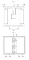
- FIG. 1 is a plan view showing a solar cell module according to the embodiment
- FIG. 2 is a sectional view taken along line I-II of FIG. 1 ;
- FIG. 3 is a bottom view showing the solar cell module according to the embodiment.
- FIG. 4 is a bottom view showing a solar cell module according to a modification
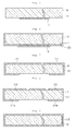
- FIGS. 5 to 8 are sectional views showing the manufacturing process of a solar cell according to a first embodiment.
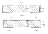
- FIGS. 9 to 11 are sectional views showing the manufacturing process of a solar cell according to a second embodiment.
- FIG. 1 is a plan view showing a solar cell module according to the embodiment
- FIG. 2 is a sectional view taken along line I-II of FIG. 1
- FIG. 3 is a bottom view showing the solar cell module according to the embodiment.
- a solar cell module 100 includes a solar cell 110 and a junction box 120 of stably collecting electricity generated from the solar cell 110 to prevent the reversal current of the electricity.
- the solar cell 110 includes a support substrate 10, a photoelectric conversion part 20 formed on the support substrate 10, and a collecting electrode 30 to collect electricity generated from the photoelectric conversion part 20.
- a plurality of photoelectric conversion parts 20 are provided, and adjacent photoelectric conversion parts 20 are connected to each other in series, thereby defining a plurality of cells.
- the details thereof will be made in detail below.
- the support substrate 10 has a plate shape, and supports the photoelectric conversion part 20 and the collecting electrode 30 formed thereon.
- the support substrate 10 may include an insulator including glass or plastic.
- the support substrate 10 may include soda lime glass.
- the embodiment is not limited thereto, and the support substrate 10 may include a metallic substrate.
- the support substrate 10 may include a rigid material or a flexible material according to the characteristics of the solar cell module 100.
- Each photoelectric conversion part 20 formed on a first surface 12 includes a first electrode 21, a light absorbing layer 23, and a second electrode (window layer) 29.
- first electrode 21 a first electrode 21, a light absorbing layer 23, and a second electrode (window layer) 29.
- second electrode a second electrode
- the first electrode 21 may include a material representing superior electrical characteristics.
- the first electrode 21 may include molybdenum (Mo), copper (Cu), nickel (Ni), aluminum (Al), or the alloy thereof.
- a light absorbing layer 23 is formed on the first electrode 21 to convert the solar light into the electrical energy.
- the light absorbing layer 23 may include a non-silicon semiconductor material.
- the light absorbing layer 23 may include a group I-III-IV compound.
- the light absorbing layer 23 may include a Cu-In-Ga-Se (Cu (In, Ga) Se2; CIGS)-based crystal structure, a Cu-In-Se-based crystal structure, or a Cu-Ga-Se-based crystal structure.
- the light absorbing layer 23 may include a group II-IV compound or a group III-IV compound.
- the light absorbing layer 23 may include cadmium (Cd) -tellurium (Te) compound, or gallium (Ga)-arsenic (As) compound.
- a buffer layer 25 and a high resistance buffer layer 27 may be formed on the light absorbing layer 23.
- the buffer layer 25 is formed on the light absorbing layer 23 to reduce the difference in the lattice constant and the energy bandgap from the second electrode 29.
- the buffer layer 25 may include CdS.
- the high resistance buffer layer 27 prevents the buffer layer 25 from being damaged when forming the second electrode 29.
- the high resistance buffer layer 27 may include zinc oxide (ZnO).
- the second electrode 29 may include a transparent conductive material which is transparent to allow light to be incident into the second electrode 29 and provides the function of an electrode due to the conductivity thereof.
- the second electrode 29 has the characteristic of an N type semiconductor to form an N type semiconductor layer together with the buffer layer 25, thereby forming a PN junction structure together with the light absorbing layer 23 serving as a P type semiconductor layer.
- the second electrode 29 may include Al doped zinc oxide (AZO).
- the light absorbing layer 23 including a CIGS-based compound, a CIS-based compound, a CGS-based compound, a Cd-Te compound, or a Ga-As compound
- the light absorbing layer 23 can represent superior photoelectric conversion efficiency.
- the solar cell module 100 is formed with a thin thickness, so that the material can be saved, and the use range of the solar cell module 100 can be expanded.
- the degradation of the light absorbing layer 23 caused by the light is reduced, so that the life span of the solar cell module 100 can be increased.
- the solar cell module 100 may include a photoelectric conversion part constituting a dye-sensitized solar cell, an organic solar cell, and a silicon solar cell.
- Each photoelectric conversion part 20 corresponds to a cell C of each solar cell 110, and the adjacent photoelectric conversion parts 20 are connected to each other in series.
- the first electrodes 21 may be spaced apart from each other while representing a pattern corresponding to the cell C of each solar cell 110.
- the light absorbing layer 23, the buffer layer 25, the high resistance buffer layer 27, and the second electrode 29 may be divided by a division pattern 44 corresponding to a cell of each solar cell 10.
- the first electrode 21 corresponding to a specific cell C may be connected to the second electrode 29 corresponding to a cell C adjacent to the specific cell C through a contact pattern 42 formed in the light absorbing layer 23, the buffer layer 25, and the high resistance buffer layer 27.
- each photoelectric conversion part 20 corresponding to the cell C of each solar cell 110 may be defined as the region in which the first electrode 21, the light absorbing layer 23, the buffer layer 25, the high resistance buffer layer 27, and the second electrode 29 are sequentially laminated on each other.
- the collecting electrode 30 is electrically connected to at least one of the first and second electrodes 21 and 29 of the photoelectric conversion parts 20 to collect current.
- the collecting electrode 30 includes first and second collecting electrodes 31 and 32, and the first and second collecting electrodes 31 and 32 are positioned at the extension parts 214a and 214b of the first electrode 21.
- the first electrode 21 includes an electrode part 212 constituting the photoelectric conversion part 20 while being placed on the top surface 12 of the support substrate 10 and the extension parts 214a and 214b extending from the top surface 12 of the support substrate 10 to a second surface 14 (the bottom of the drawings; hereinafter, referred to as "bottom surface").
- the extension parts 214a and 214b include the first extension part 214a extending from the electrode part 212 placed at one side (the left side of the drawings; hereinafter, referred to as a left side) of the support substrate 10 toward the bottom surface 14 of the support substrate 10, and the second extension part 214b extending from the electrode part 212 placed at an opposite side (the right side of the drawings; hereinafter, referred to as a right side) of the support substrate 10 toward the bottom surface 14 of the support substrate 10.
- the first and second extension parts 214a and 214b are spaced apart from each other on the bottom surface 14 of the support substrate 10.
- the first extension part 214a extends from the electrode part 212 (the most left side electrode part in the drawings) of the first electrode 21 without the contact pattern 42
- the second extension part 214b extends from the electrode part 212 (the most right side electrode part in the drawings) of the first electrode 21 directly connected to the second electrode 29 through the contact pattern 42. Accordingly, both of the first and second collecting electrodes 31 and 32 can be placed on the same first electrode 21, and the photoelectric conversion parts 20 can be connected to each other in series.
- the first collecting electrode 31 may make contact with the first extension part 214a on the bottom surface 14 of the support substrate 10, and the second collecting electrode 32 may make contact with the second extension part 214b on the bottom surface 14 of the support substrate 10.
- the area of the photoelectric conversion part 20 provided on the top surface 12 of the support substrate 10 can be maximized.
- the area of the photoelectric conversion part 20 since the first and second collecting electrodes 31 and 32 are formed on the top surface 12 of the support substrate 10 together with the photoelectric conversion part 20, the area of the photoelectric conversion part 20 must be reduced by the area of the first and second collecting electrodes 31 and 32. Accordingly, the effective area of the solar cell 110 is reduced.
- the first and second collecting electrodes 31 and 32 are formed on a surface different from that of the photoelectric conversion part 20, the area, in which the photoelectric conversion part 20 is formed, is maximized, so that the effective area of the solar cell 110 can be increased.
- the first and second extension parts 214a and 214b and the first and second collecting electrodes 31 and 32 are provided on the bottom surface 14 of the support substrate 10 that does not receive the solar light, the first and second extension parts 214a and 214b and the first and second collecting electrodes 31 and 32 may be formed with a wide area. Therefore, the efficiency of the solar cell 110 can be improved by reducing contact resistance.
- first and second extension parts 214a and 214b may be spaced apart from each other by the distance of about 60 ⁇ m or more on the bottom surface 14 of the support substrate 10. Inotherwords, since the first and second extension parts 214a and214b are spaced apart from each other to the extent that the first extension part 214a is not electrically connected to the second extension part 214b, the areas of the first and second extension parts 214a and 214b and the first and second collecting electrodes 31 and 32 can be maximized.
- extension parts 216a and 216b may include protrusion parts P1 and P2, the protrusion P1 of the first extension part 216a and the protrusion part P2 of the second extension part 216b may be alternately provided, and the first and second collecting electrodes 131 and 132 may have shapes corresponding to the first and second extension parts 216a and 216b.
- first and second extension parts and the first and second collecting electrodes may be variously modified, and the modifications are within the technical scope of the present embodiment.
- a protective film reference numeral 50 of FIG. 2
- the junction box reference numeral 120 of FIG. 3
- the first and second extension parts 214a and 214b surround the lateral side of the support substrate 10 while extending to the bottom surface 14 of the support substrate 10. Accordingly, the first and second collecting electrodes 31 and 32 can be positioned on the bottom surface 14 of the support substrate 10 in the simple structure. In other words, the first and second collecting electrodes 31 and 32 can be positioned on the bottom surface 14 of the support substrate 10 through the simple manufacturing process without the process of forming additionally through holes in the support substrate 10.
- the collecting electrode 30 is formed on the first electrode 21 adj acent to the support substrate 10 according to the present embodiment, the present embodiment is not limited thereto. Therefore, the collecting electrode 30 may be formed on the second electrode 29, or may be formed on each of the first and second electrodes 21 and 29.
- a protective film 50 surrounds the solar cell 110 to protect the solar cell 110, and an insulating sealing member 60 is formed at the lateral side of the solar cell 110 to make the solar cell 110 in the form of a module.
- the material constituting the solar cell 110 can be firmly fixed by using the frame 70 surrounding the solar cell 110.
- the junction box 120 may be positioned on the protective film 50 formed on the bottom surface 14 of the support substrate 10 having the first and second collecting electrodes 31 and 32.
- the first junction box 120 may receive a circuit board having diodes mounted thereon, and may be connected to the first and second collecting electrodes 31 and 32 through a cable 122.
- an additional hole used to connect the first and second collecting electrodes 31 and 32 to the junction box 120 may not be formed in the support substrate 10.
- the connection structure of the first and second collecting electrodes 31 and 32 and the junction box 120 can be simplified, the size of the solar cell module 100 can be reduced, and the manufacturing process of the solar cell module 100 can be simplified.
- the embodiment is not limited thereto, and the junction box 120 and the cable 122 may not be formed.
- FIGS. 5 to 8 are sectional views showing the manufacturing process of the solar cell according to the first embodiment.
- a tape 16 is formed on the bottom surface 14 of the support substrate 10.
- the tape 16 may be formed in a region without the first extension part (reference numeral 214a of FIG. 2 ) and the second extension part (reference numeral 214b of FIG. 2 ).
- the tape 16 may include a mask material such as metal, ceramic, or polymer.
- a conductive material layer 220 including a conductive material is formed on the whole surface of the support substrate 10.
- the conductive material is formed on all of the front surface, the rear surface, and the lateral side of the support substrate 10 by tilting a source to supply the conductive material and/or the support substrate 10.
- the deposition scheme may include various processes such as an electrochemical vapor deposition (EVD) process, or a spray process.
- the tape (reference numeral 16 of FIG. 5c) is removed.
- the conductive material layer 220 formed on the tape 16 is removed, thereby forming the first electrode layer 222 including the electrode part and the first and second extension part.
- the first electrode 21 including the electrode part 212 having a pattern corresponding to each cell is formed by patterning the first electrode layer 222.
- the contact pattern (reference numeral 42 of FIG. 2 ) may be formed, the second electrode (reference numeral 29 of FIG. 2 ) may be formed, and the division pattern (reference numeral 44 of FIG. 2 ) may be formed. Accordingly, the solar cell 110 of FIG. 2 may be formed. Since the above process may be variously performed, the detail thereof will be omitted.
- the first electrode 21 having the first and second extension parts 214a and 214b may be formed on the bottom surface 14 of the support substrate 10 through the simple process.
- tape 16 is used according to the embodiment described above, various schemes such as a scheme of using a mask may be employed.
- FIGS. 9 to 11 are sectional views showing the manufacturing process in a method of fabricating the solar cell according to the second embodiment.
- the details of a process identical to or similar to a process of the first embodiment will be omitted, and the process different from the process of the first embodiment will be described.
- a conductive material layer 220 is formed on the whole surface of the support substrate 10 by dipping the support substrate 10 into a plating solution.
- the first electrode layer 232 may be formed by removing the conductive material layer (reference numeral 230 of FIG. 5a) of the first extension part (reference numeral 214a of FIG. 2 ) and the second extension part (reference numeral 214b of FIG. 2 ).
- a mechanical scheme of performing a scribing process using a tip a laser scheme, an etching scheme, or a sand blast scheme may be used.
- the first electrode 21 including the electrode part 212 having a pattern corresponding to each solar cell is formed by patterning the first electrode layer 232.
- the contact pattern (reference numeral 42 of FIG. 2 ) is formed, and the second electrode (reference numeral 29 of FIG. 2 ) is formed.
- the division pattern (reference numeral 44 of FIG. 2 ) may be formed. Therefore, the solar cell 110 of FIG. 2 may be formed. Since the above process can be variously performed, the detail thereof will be omitted.
- any reference in this specification to "one embodiment,” “an embodiment,” “example embodiment,” etc. means that a particular feature, structure, or characteristic described in connection with the embodiment is included in at least one embodiment of the invention.
- the appearances of such phrases in various places in the specification are not necessarily all referring to the same embodiment.
Landscapes
- Engineering & Computer Science (AREA)
- Power Engineering (AREA)
- Microelectronics & Electronic Packaging (AREA)
- Photovoltaic Devices (AREA)
Abstract
Description
- The embodiment relates to a solar cell and a solar cell module including the same.
- Recently, as energy consumption is increased, a solar cell has been developed to convert solar energy into electrical energy. The solar cell has an important issue to improve the photoelectric conversion efficiency.
- The embodiment provides a solar cell capable of increasing an effective region which can generate electrical energy by absorbing the solar light, and a solar cell module including the same.
- According to the embodiment, there is provided a solar cell including a support substrate having first and second surfaces opposite to each other, a photoelectric conversion part disposed on the first surface and including a first electrode, a light absorbing layer, and a second electrode, and a collecting electrode electrically connected to at least one of the first and second electrodes and disposed on the second surface.
- Meanwhile, a solar cell module according to the embodiment includes the solar cell and a junction box disposed on the second surface of the support substrate.
- As described above, according to the solar cell of the embodiment, since the collecting electrode is positioned on the bottom surface of the support substrate, the area of the photoelectric conversion part positioned on the top surface of the support substrate can be maximized. Accordingly, the effective area of the solar cell can be increased. In addition, since the extension part and the collecting electrode are positioned on the bottom surface of the support substrate, which does not receive the solar light, the extension part and the collecting electrode can be formed with the wide area. Accordingly, the contact resistance can be reduced so that the efficiency of the solar cell can be improved.
- In addition, since the extension part extends to the bottom surface of the support substrate while surrounding the lateral side of the support substrate. Accordingly, the collect electrode can be positioned on the bottom surface of the support substrate in the simple structure.
- In addition, since the junction box is positioned on the bottom surface of the support substrate, the collecting electrode can be aligned in line with the junction box. Accordingly, the connection structure between the collecting electrode and the junction box can be simplified.
-
FIG. 1 is a plan view showing a solar cell module according to the embodiment; -
FIG. 2 is a sectional view taken along line I-II ofFIG. 1 ; -
FIG. 3 is a bottom view showing the solar cell module according to the embodiment; -
FIG. 4 is a bottom view showing a solar cell module according to a modification; -
FIGS. 5 to 8 are sectional views showing the manufacturing process of a solar cell according to a first embodiment; and -
FIGS. 9 to 11 are sectional views showing the manufacturing process of a solar cell according to a second embodiment. - In the description of the embodiments, it will be understood that, when a layer (or film), a region, a pattern, or a structure is referred to as being "on" or "under" another substrate, another layer (or film), another region, another pad, or another pattern, it can be "directly" or "indirectly" on the other substrate, layer (or film), region, pad, or pattern, or one or more intervening layers may also be present. The thickness and size of each layer (or film), each region, each pattern, or each structure shown in the drawings may be exaggerated, omitted or schematically drawn for the purpose of convenience or clarity. In addition, the size of elements does not utterly reflect an actual size.
- Hereinafter, the embodiment will be described in detail with reference to accompanying drawings.
-
FIG. 1 is a plan view showing a solar cell module according to the embodiment,FIG. 2 is a sectional view taken along line I-II ofFIG. 1 , andFIG. 3 is a bottom view showing the solar cell module according to the embodiment. - Referring to
FIGS. 1 to 3 , asolar cell module 100 according to the embodiment includes asolar cell 110 and ajunction box 120 of stably collecting electricity generated from thesolar cell 110 to prevent the reversal current of the electricity. - In this case, referring to
FIG. 2 , thesolar cell 110 includes asupport substrate 10, aphotoelectric conversion part 20 formed on thesupport substrate 10, and a collectingelectrode 30 to collect electricity generated from thephotoelectric conversion part 20. According to the present embodiment, a plurality ofphotoelectric conversion parts 20 are provided, and adjacentphotoelectric conversion parts 20 are connected to each other in series, thereby defining a plurality of cells. Hereinafter, the details thereof will be made in detail below. - The
support substrate 10 has a plate shape, and supports thephotoelectric conversion part 20 and the collectingelectrode 30 formed thereon. Thesupport substrate 10 may include an insulator including glass or plastic. For example, thesupport substrate 10 may include soda lime glass. However, the embodiment is not limited thereto, and thesupport substrate 10 may include a metallic substrate. In other words, thesupport substrate 10 may include a rigid material or a flexible material according to the characteristics of thesolar cell module 100. - Each
photoelectric conversion part 20 formed on a first surface 12 (the top in drawings; hereinafter, referred to as "top surface") includes afirst electrode 21, alight absorbing layer 23, and a second electrode (window layer) 29. Hereinafter, the connection structure of adjacentphotoelectric conversion parts 20 will be described after describing thephotoelectric conversion parts 20 while focusing on onephotoelectric conversion part 30. - The
first electrode 21 may include a material representing superior electrical characteristics. For example, thefirst electrode 21 may include molybdenum (Mo), copper (Cu), nickel (Ni), aluminum (Al), or the alloy thereof. - A
light absorbing layer 23 is formed on thefirst electrode 21 to convert the solar light into the electrical energy. According to the present embodiment, thelight absorbing layer 23 may include a non-silicon semiconductor material. - The
light absorbing layer 23 may include a group I-III-IV compound. For example, thelight absorbing layer 23 may include a Cu-In-Ga-Se (Cu (In, Ga) Se2; CIGS)-based crystal structure, a Cu-In-Se-based crystal structure, or a Cu-Ga-Se-based crystal structure. - In addition, the
light absorbing layer 23 may include a group II-IV compound or a group III-IV compound. For example, thelight absorbing layer 23 may include cadmium (Cd) -tellurium (Te) compound, or gallium (Ga)-arsenic (As) compound. - A
buffer layer 25 and a high resistance buffer layer 27 may be formed on thelight absorbing layer 23. - The
buffer layer 25 is formed on thelight absorbing layer 23 to reduce the difference in the lattice constant and the energy bandgap from thesecond electrode 29. For example, thebuffer layer 25 may include CdS. - The high resistance buffer layer 27 prevents the
buffer layer 25 from being damaged when forming thesecond electrode 29. For example, the high resistance buffer layer 27 may include zinc oxide (ZnO). - The
second electrode 29 may include a transparent conductive material which is transparent to allow light to be incident into thesecond electrode 29 and provides the function of an electrode due to the conductivity thereof. In addition, thesecond electrode 29 has the characteristic of an N type semiconductor to form an N type semiconductor layer together with thebuffer layer 25, thereby forming a PN junction structure together with thelight absorbing layer 23 serving as a P type semiconductor layer. To this end, for example, thesecond electrode 29 may include Al doped zinc oxide (AZO). - According to the present embodiment, since the
light absorbing layer 23 including a CIGS-based compound, a CIS-based compound, a CGS-based compound, a Cd-Te compound, or a Ga-As compound is provided, thelight absorbing layer 23 can represent superior photoelectric conversion efficiency.Accordingly, thesolar cell module 100 is formed with a thin thickness, so that the material can be saved, and the use range of thesolar cell module 100 can be expanded. In addition, the degradation of thelight absorbing layer 23 caused by the light is reduced, so that the life span of thesolar cell module 100 can be increased. - However, the present embodiment is not limited thereto. Accordingly, the
solar cell module 100 may include a photoelectric conversion part constituting a dye-sensitized solar cell, an organic solar cell, and a silicon solar cell. - Each
photoelectric conversion part 20 corresponds to a cell C of eachsolar cell 110, and the adjacentphotoelectric conversion parts 20 are connected to each other in series. In more detail, thefirst electrodes 21 may be spaced apart from each other while representing a pattern corresponding to the cell C of eachsolar cell 110. In addition, thelight absorbing layer 23, thebuffer layer 25, the high resistance buffer layer 27, and thesecond electrode 29 may be divided by adivision pattern 44 corresponding to a cell of eachsolar cell 10. Thefirst electrode 21 corresponding to a specific cell C may be connected to thesecond electrode 29 corresponding to a cell C adjacent to the specific cell C through acontact pattern 42 formed in thelight absorbing layer 23, thebuffer layer 25, and the high resistance buffer layer 27. - Therefore, each
photoelectric conversion part 20 corresponding to the cell C of eachsolar cell 110 may be defined as the region in which thefirst electrode 21, thelight absorbing layer 23, thebuffer layer 25, the high resistance buffer layer 27, and thesecond electrode 29 are sequentially laminated on each other. - The collecting
electrode 30 is electrically connected to at least one of the first andsecond electrodes photoelectric conversion parts 20 to collect current. According to the present embodiment, the collectingelectrode 30 includes first andsecond collecting electrodes second collecting electrodes extension parts first electrode 21. - In more detail, the
first electrode 21 includes anelectrode part 212 constituting thephotoelectric conversion part 20 while being placed on thetop surface 12 of thesupport substrate 10 and theextension parts top surface 12 of thesupport substrate 10 to a second surface 14 (the bottom of the drawings; hereinafter, referred to as "bottom surface"). Theextension parts first extension part 214a extending from theelectrode part 212 placed at one side (the left side of the drawings; hereinafter, referred to as a left side) of thesupport substrate 10 toward thebottom surface 14 of thesupport substrate 10, and thesecond extension part 214b extending from theelectrode part 212 placed at an opposite side (the right side of the drawings; hereinafter, referred to as a right side) of thesupport substrate 10 toward thebottom surface 14 of thesupport substrate 10. The first andsecond extension parts bottom surface 14 of thesupport substrate 10. - In this case, the
first extension part 214a extends from the electrode part 212 (the most left side electrode part in the drawings) of thefirst electrode 21 without thecontact pattern 42, and thesecond extension part 214b extends from the electrode part 212 (the most right side electrode part in the drawings) of thefirst electrode 21 directly connected to thesecond electrode 29 through thecontact pattern 42. Accordingly, both of the first andsecond collecting electrodes first electrode 21, and thephotoelectric conversion parts 20 can be connected to each other in series. - The
first collecting electrode 31 may make contact with thefirst extension part 214a on thebottom surface 14 of thesupport substrate 10, and thesecond collecting electrode 32 may make contact with thesecond extension part 214b on thebottom surface 14 of thesupport substrate 10. - As described above, according to the present embodiment, since the first and
second collecting electrodes bottom surface 14 of thesupport substrate 10, the area of thephotoelectric conversion part 20 provided on thetop surface 12 of thesupport substrate 10 can be maximized. In addition, according to the related art, since the first andsecond collecting electrodes top surface 12 of thesupport substrate 10 together with thephotoelectric conversion part 20, the area of thephotoelectric conversion part 20 must be reduced by the area of the first andsecond collecting electrodes solar cell 110 is reduced. However, according to the present embodiment, since the first andsecond collecting electrodes photoelectric conversion part 20, the area, in which thephotoelectric conversion part 20 is formed, is maximized, so that the effective area of thesolar cell 110 can be increased. - Inaddition, since the first and
second extension parts second collecting electrodes bottom surface 14 of thesupport substrate 10 that does not receive the solar light, the first andsecond extension parts second collecting electrodes solar cell 110 can be improved by reducing contact resistance. - In this case, the first and
second extension parts bottom surface 14 of thesupport substrate 10. Inotherwords, since the first andsecond extension parts 214a and214b are spaced apart from each other to the extent that thefirst extension part 214a is not electrically connected to thesecond extension part 214b, the areas of the first andsecond extension parts second collecting electrodes - Although
FIG. 3 shows that theextension parts second collecting electrodes FIG. 4 ,extension parts first extension part 216a and the protrusion part P2 of thesecond extension part 216b may be alternately provided, and the first andsecond collecting electrodes second extension parts - As described above, the first and second extension parts and the first and second collecting electrodes may be variously modified, and the modifications are within the technical scope of the present embodiment. For reference, a protective film (
reference numeral 50 ofFIG. 2 ) and the junction box (reference numeral 120 ofFIG. 3 ) are not shown inFIG. 4 for the brief description. - Referring to
FIGS. 1 and 2 again, the first andsecond extension parts support substrate 10 while extending to thebottom surface 14 of thesupport substrate 10. Accordingly, the first andsecond collecting electrodes bottom surface 14 of thesupport substrate 10 in the simple structure. In other words, the first andsecond collecting electrodes bottom surface 14 of thesupport substrate 10 through the simple manufacturing process without the process of forming additionally through holes in thesupport substrate 10. - For example, although the collecting
electrode 30 is formed on thefirst electrode 21 adj acent to thesupport substrate 10 according to the present embodiment, the present embodiment is not limited thereto. Therefore, the collectingelectrode 30 may be formed on thesecond electrode 29, or may be formed on each of the first andsecond electrodes - In addition, a
protective film 50 surrounds thesolar cell 110 to protect thesolar cell 110, and an insulating sealingmember 60 is formed at the lateral side of thesolar cell 110 to make thesolar cell 110 in the form of a module. In addition, the material constituting thesolar cell 110 can be firmly fixed by using theframe 70 surrounding thesolar cell 110. - In addition, referring to
FIG. 3 , thejunction box 120 may be positioned on theprotective film 50 formed on thebottom surface 14 of thesupport substrate 10 having the first andsecond collecting electrodes first junction box 120 may receive a circuit board having diodes mounted thereon, and may be connected to the first andsecond collecting electrodes cable 122. According to the present embodiment, since the first andsecond collecting electrodes junction box 120, an additional hole used to connect the first andsecond collecting electrodes junction box 120 may not be formed in thesupport substrate 10. As described above, since the connection structure of the first andsecond collecting electrodes junction box 120 can be simplified, the size of thesolar cell module 100 can be reduced, and the manufacturing process of thesolar cell module 100 can be simplified. - However, the embodiment is not limited thereto, and the
junction box 120 and thecable 122 may not be formed. - Hereinafter, the method of manufacturing the solar cell according to the first embodiment will be described in more detail with reference to
FIGS. 5 to 8. FIGS. 5 to 8 are sectional views showing the manufacturing process of the solar cell according to the first embodiment. - First, as shown in
FIG. 5 , atape 16 is formed on thebottom surface 14 of thesupport substrate 10. Thetape 16 may be formed in a region without the first extension part (reference numeral 214a ofFIG. 2 ) and the second extension part (reference numeral 214b ofFIG. 2 ). - The
tape 16 may include a mask material such as metal, ceramic, or polymer. - Thereafter, as shown in
FIG. 6 , aconductive material layer 220 including a conductive material is formed on the whole surface of thesupport substrate 10. When performing the process of forming theconductive material layer 220, the conductive material is formed on all of the front surface, the rear surface, and the lateral side of thesupport substrate 10 by tilting a source to supply the conductive material and/or thesupport substrate 10. The deposition scheme may include various processes such as an electrochemical vapor deposition (EVD) process, or a spray process. - Thereafter, as shown in
FIG. 7 , the tape (reference numeral 16 of FIG. 5c) is removed. In this case, theconductive material layer 220 formed on thetape 16 is removed, thereby forming thefirst electrode layer 222 including the electrode part and the first and second extension part. - Subsequently, as shown in
FIG. 8 , thefirst electrode 21 including theelectrode part 212 having a pattern corresponding to each cell is formed by patterning thefirst electrode layer 222. - Then, after forming the light absorbing layer (
reference numeral 23 ofFig. 2 ), the buffer layer (reference numeral 25 ofFIG. 2 ), and the high resistance buffer layer (reference number 27 ofFIG. 2 ), the contact pattern (reference numeral 42 ofFIG. 2 ) may be formed, the second electrode (reference numeral 29 ofFIG. 2 ) may be formed, and the division pattern (reference numeral 44 ofFIG. 2 ) may be formed. Accordingly, thesolar cell 110 ofFIG. 2 may be formed. Since the above process may be variously performed, the detail thereof will be omitted. - According to the present embodiment, the
first electrode 21 having the first andsecond extension parts bottom surface 14 of thesupport substrate 10 through the simple process. - Although the
tape 16 is used according to the embodiment described above, various schemes such as a scheme of using a mask may be employed. - Hereinafter, a method of fabricating a solar cell according to a second embodiment will be described with reference to
FIGS. 9 to 11. FIGS. 9 to 11 are sectional views showing the manufacturing process in a method of fabricating the solar cell according to the second embodiment. Hereinafter, the details of a process identical to or similar to a process of the first embodiment will be omitted, and the process different from the process of the first embodiment will be described. - First, as shown in
FIG. 9 , aconductive material layer 220 is formed on the whole surface of thesupport substrate 10 by dipping thesupport substrate 10 into a plating solution. - Therefore, as shown in
FIG. 10 , thefirst electrode layer 232 may be formed by removing the conductive material layer (reference numeral 230 of FIG. 5a) of the first extension part (reference numeral 214a ofFIG. 2 ) and the second extension part (reference numeral 214b ofFIG. 2 ). In order to remove the conductive material layer 230 between the first andsecond extension parts - Thereafter, as shown in
FIG. 11 , thefirst electrode 21 including theelectrode part 212 having a pattern corresponding to each solar cell is formed by patterning thefirst electrode layer 232. - Thereafter, after forming the light absorbing layer (
reference numeral 23 ofFIG. 2 ), the buffer layer (reference numeral 25 ofFIG. 2 ), and the high reference buffer layer (reference numeral 27 ofFIG. 2 ), the contact pattern (reference numeral 42 ofFIG. 2 ) is formed, and the second electrode (reference numeral 29 ofFIG. 2 ) is formed. Thereafter, the division pattern (reference numeral 44 ofFIG. 2 ) may be formed. Therefore, thesolar cell 110 ofFIG. 2 may be formed. Since the above process can be variously performed, the detail thereof will be omitted. - Any reference in this specification to "one embodiment," "an embodiment," "example embodiment," etc., means that a particular feature, structure, or characteristic described in connection with the embodiment is included in at least one embodiment of the invention. The appearances of such phrases in various places in the specification are not necessarily all referring to the same embodiment. Further, when a particular feature, structure, or characteristic is described in connection with any embodiment, it is submitted that it is within the purview of one skilled in the art to effect such feature, structure, or characteristic in connection with other ones of the embodiments.
- Although embodiments have been described with reference to a number of illustrative embodiments thereof, it should be understood that numerous other modifications and embodiments can be devised by those skilled in the art that will fall within the spirit and scope of the principles of this disclosure. More particularly, various variations and modifications are possible in the component parts and/or arrangements of the subject combination arrangement within the scope of the disclosure, the drawings and the appended claims. In addition to variations and modifications in the component parts and/or arrangements, alternative uses will also be apparent to those skilled in the art.
Claims (10)
- A solar cell comprising:a support substrate having first and second surfaces opposite to each other;a photoelectric conversion part disposed on the first surface and including a first electrode, a light absorbing layer, and a second electrode; anda collecting electrode electrically connected to at least one of the first and second electrodes and disposed on the second surface.
- The solar cell of claim 1, wherein at least one of the first and second electrodes includes an electrode part disposed on the first surface and an extension part extending from the first surface to the second surface, and the collecting electrode makes contact with the extension part.
- The solar cell of claim 2, wherein the extension part extends from the first surface to the second surface while surrounding a lateral side of the support substrate.
- The solar cell of claim 1, wherein the first electrode, the light absorbing layer, and the second electrode are sequentially laminated on the first surface of the support substrate, and the first electrode comprises an electrode layer positioned on the first surface and an extension part extending from the first surface to the second surface.
- The solar cell of claim 4, wherein first and second extension parts have a width of about 60µm or more.
- The solar cell of claim 4, wherein the extension part comprises a first extension part extending from one side of the electrode part and a second extension part extending from an opposite side of the electrode part and spaced apart from the first extension part on the second surface, and
wherein the collecting electrode comprises a first collecting electrode making contact with the first extension part and a second collecting electrode making contact with the second extension part. - The solar cell of claim 6, wherein the photoelectric conversion part includes a plurality of photoelectric conversion parts connected to each other in series, so that the electrode part of the first electrode, the light absorbing layer, and the second electrode comprises a plurality of electrode parts, a plurality of light absorbing layers, and a plurality of second electrodes, respectively, and
wherein the first extension part extends from the electrode part of the first electrode that is not connected to the second electrode through a contact pattern, and the second extension part extends from the electrode part of the first electrode that is connected to the second electrode through the contact pattern. - A solar cell module comprising:a solar cell comprising a support substrate having first and second surfaces opposite to each other; a photoelectric conversion part disposed on the first surface and including a first electrode, a light absorbing layer, and a second electrode; and a collecting electrode electrically connected to at least one of the first and second electrodes and disposed on the second surface; anda junction box on the second surface of the support substrate.
- The solar cell module of claim 8, wherein at least one of the first and second electrodes includes an electrode part on the first surface and an extension part extending from the first surface to the second surface, and the collecting electrode makes contact with the extension part.
- The solar cell module of claim 9, wherein the extension part extends from the first surface to the second surface while surrounding a lateral side of the support substrate.
Applications Claiming Priority (2)
| Application Number | Priority Date | Filing Date | Title |
|---|---|---|---|
| KR1020100085582A KR101154718B1 (en) | 2010-09-01 | 2010-09-01 | Solar cell and solar cell module including the same |
| PCT/KR2011/003122 WO2012030047A1 (en) | 2010-09-01 | 2011-04-27 | Solar cell and solar cell module including same |
Publications (3)
| Publication Number | Publication Date |
|---|---|
| EP2610921A1 true EP2610921A1 (en) | 2013-07-03 |
| EP2610921A4 EP2610921A4 (en) | 2018-01-03 |
| EP2610921B1 EP2610921B1 (en) | 2019-11-20 |
Family
ID=45773086
Family Applications (1)
| Application Number | Title | Priority Date | Filing Date |
|---|---|---|---|
| EP11822022.7A Active EP2610921B1 (en) | 2010-09-01 | 2011-04-27 | Solar cell and solar cell module including same |
Country Status (5)
| Country | Link |
|---|---|
| EP (1) | EP2610921B1 (en) |
| JP (1) | JP5775586B2 (en) |
| KR (1) | KR101154718B1 (en) |
| CN (1) | CN103053030B (en) |
| WO (1) | WO2012030047A1 (en) |
Families Citing this family (1)
| Publication number | Priority date | Publication date | Assignee | Title |
|---|---|---|---|---|
| CN114759101B (en) * | 2020-12-29 | 2023-08-01 | 隆基绿能科技股份有限公司 | Hot carrier solar cell and photovoltaic module |
Family Cites Families (9)
| Publication number | Priority date | Publication date | Assignee | Title |
|---|---|---|---|---|
| JPS61163671A (en) * | 1985-01-16 | 1986-07-24 | Matsushita Electric Ind Co Ltd | thin film solar cells |
| JP2992638B2 (en) * | 1995-06-28 | 1999-12-20 | キヤノン株式会社 | Electrode structure and manufacturing method of photovoltaic element and solar cell |
| JP3551787B2 (en) * | 1998-10-14 | 2004-08-11 | 富士電機アドバンストテクノロジー株式会社 | Solar cell module and method of manufacturing the same |
| JP2004079752A (en) * | 2002-08-16 | 2004-03-11 | Rikogaku Shinkokai | Tape-like solar cell |
| JP4798956B2 (en) | 2004-03-29 | 2011-10-19 | 京セラ株式会社 | Solar cell module and solar power generation apparatus using the same |
| JP2006216608A (en) * | 2005-02-01 | 2006-08-17 | Honda Motor Co Ltd | Solar cell module |
| JP2009065022A (en) * | 2007-09-07 | 2009-03-26 | Fuji Electric Systems Co Ltd | Thin film solar cell and manufacturing method thereof |
| WO2009097588A2 (en) * | 2008-01-30 | 2009-08-06 | Xunlight Corporation | Series interconnected thin-film photovoltaic module and method for preparation thereof |
| JP5676280B2 (en) * | 2008-03-11 | 2015-02-25 | サン−ゴバン グラス フランス エス アー | Solar module |
-
2010
- 2010-09-01 KR KR1020100085582A patent/KR101154718B1/en not_active Expired - Fee Related
-
2011
- 2011-04-27 JP JP2013526988A patent/JP5775586B2/en not_active Expired - Fee Related
- 2011-04-27 WO PCT/KR2011/003122 patent/WO2012030047A1/en not_active Ceased
- 2011-04-27 CN CN201180037775.0A patent/CN103053030B/en not_active Expired - Fee Related
- 2011-04-27 EP EP11822022.7A patent/EP2610921B1/en active Active
Also Published As
| Publication number | Publication date |
|---|---|
| EP2610921A4 (en) | 2018-01-03 |
| WO2012030047A1 (en) | 2012-03-08 |
| JP2013536997A (en) | 2013-09-26 |
| KR20120022229A (en) | 2012-03-12 |
| CN103053030B (en) | 2016-04-27 |
| KR101154718B1 (en) | 2012-06-08 |
| CN103053030A (en) | 2013-04-17 |
| EP2610921B1 (en) | 2019-11-20 |
| JP5775586B2 (en) | 2015-09-09 |
Similar Documents
| Publication | Publication Date | Title |
|---|---|---|
| KR100999797B1 (en) | Photovoltaic device and its manufacturing method | |
| US20120174977A1 (en) | Solar Power Generation Apparatus and Manufacturing Method Thereof | |
| US8779282B2 (en) | Solar cell apparatus and method for manufacturing the same | |
| KR101283072B1 (en) | Solar cell apparatus and method of fabricating the same | |
| US9502591B2 (en) | Device for generating photovoltaic power and manufacturing method for same | |
| US20130180566A1 (en) | Device for generating photovoltaic power and method for manufacturing same | |
| KR101114079B1 (en) | Solar cell apparatus and method of fabricating the same | |
| US9954484B2 (en) | Solar battery module | |
| US9391219B2 (en) | Photovoltaic apparatus | |
| US9954122B2 (en) | Solar cell apparatus and method of fabricating the same | |
| US9837557B2 (en) | Solar cell apparatus and method of fabricating the same | |
| EP2610921B1 (en) | Solar cell and solar cell module including same | |
| CN103069574B (en) | Photovoltaic power generation equipment and manufacture method thereof | |
| CN102576760A (en) | Photovoltaic device and manufacturing method thereof | |
| US20130019943A1 (en) | Solar power generating device, and method for manufacturing same | |
| WO2013174056A1 (en) | Solar cell | |
| KR101349525B1 (en) | Photovoltaic apparatus | |
| KR101382995B1 (en) | Solar cell and method of fabricating the same | |
| KR20130077010A (en) | A solar cell and a manufacturing method thereof |
Legal Events
| Date | Code | Title | Description |
|---|---|---|---|
| PUAI | Public reference made under article 153(3) epc to a published international application that has entered the european phase |
Free format text: ORIGINAL CODE: 0009012 |
|
| 17P | Request for examination filed |
Effective date: 20120724 |
|
| AK | Designated contracting states |
Kind code of ref document: A1 Designated state(s): AL AT BE BG CH CY CZ DE DK EE ES FI FR GB GR HR HU IE IS IT LI LT LU LV MC MK MT NL NO PL PT RO RS SE SI SK SM TR |
|
| DAX | Request for extension of the european patent (deleted) | ||
| RAP1 | Party data changed (applicant data changed or rights of an application transferred) |
Owner name: LG INNOTEK CO., LTD. |
|
| RA4 | Supplementary search report drawn up and despatched (corrected) |
Effective date: 20171201 |
|
| RIC1 | Information provided on ipc code assigned before grant |
Ipc: H01L 31/0224 20060101ALI20171127BHEP Ipc: H01L 31/042 20140101AFI20171127BHEP |
|
| GRAP | Despatch of communication of intention to grant a patent |
Free format text: ORIGINAL CODE: EPIDOSNIGR1 |
|
| STAA | Information on the status of an ep patent application or granted ep patent |
Free format text: STATUS: GRANT OF PATENT IS INTENDED |
|
| INTG | Intention to grant announced |
Effective date: 20190605 |
|
| GRAS | Grant fee paid |
Free format text: ORIGINAL CODE: EPIDOSNIGR3 |
|
| GRAA | (expected) grant |
Free format text: ORIGINAL CODE: 0009210 |
|
| STAA | Information on the status of an ep patent application or granted ep patent |
Free format text: STATUS: THE PATENT HAS BEEN GRANTED |
|
| AK | Designated contracting states |
Kind code of ref document: B1 Designated state(s): AL AT BE BG CH CY CZ DE DK EE ES FI FR GB GR HR HU IE IS IT LI LT LU LV MC MK MT NL NO PL PT RO RS SE SI SK SM TR |
|
| REG | Reference to a national code |
Ref country code: GB Ref legal event code: FG4D |
|
| REG | Reference to a national code |
Ref country code: CH Ref legal event code: EP |
|
| REG | Reference to a national code |
Ref country code: IE Ref legal event code: FG4D |
|
| REG | Reference to a national code |
Ref country code: DE Ref legal event code: R096 Ref document number: 602011063541 Country of ref document: DE |
|
| REG | Reference to a national code |
Ref country code: AT Ref legal event code: REF Ref document number: 1205174 Country of ref document: AT Kind code of ref document: T Effective date: 20191215 |
|
| REG | Reference to a national code |
Ref country code: NL Ref legal event code: MP Effective date: 20191120 |
|
| REG | Reference to a national code |
Ref country code: LT Ref legal event code: MG4D |
|
| PG25 | Lapsed in a contracting state [announced via postgrant information from national office to epo] |
Ref country code: ES Free format text: LAPSE BECAUSE OF FAILURE TO SUBMIT A TRANSLATION OF THE DESCRIPTION OR TO PAY THE FEE WITHIN THE PRESCRIBED TIME-LIMIT Effective date: 20191120 Ref country code: LT Free format text: LAPSE BECAUSE OF FAILURE TO SUBMIT A TRANSLATION OF THE DESCRIPTION OR TO PAY THE FEE WITHIN THE PRESCRIBED TIME-LIMIT Effective date: 20191120 Ref country code: NL Free format text: LAPSE BECAUSE OF FAILURE TO SUBMIT A TRANSLATION OF THE DESCRIPTION OR TO PAY THE FEE WITHIN THE PRESCRIBED TIME-LIMIT Effective date: 20191120 Ref country code: FI Free format text: LAPSE BECAUSE OF FAILURE TO SUBMIT A TRANSLATION OF THE DESCRIPTION OR TO PAY THE FEE WITHIN THE PRESCRIBED TIME-LIMIT Effective date: 20191120 Ref country code: BG Free format text: LAPSE BECAUSE OF FAILURE TO SUBMIT A TRANSLATION OF THE DESCRIPTION OR TO PAY THE FEE WITHIN THE PRESCRIBED TIME-LIMIT Effective date: 20200220 Ref country code: GR Free format text: LAPSE BECAUSE OF FAILURE TO SUBMIT A TRANSLATION OF THE DESCRIPTION OR TO PAY THE FEE WITHIN THE PRESCRIBED TIME-LIMIT Effective date: 20200221 Ref country code: NO Free format text: LAPSE BECAUSE OF FAILURE TO SUBMIT A TRANSLATION OF THE DESCRIPTION OR TO PAY THE FEE WITHIN THE PRESCRIBED TIME-LIMIT Effective date: 20200220 Ref country code: SE Free format text: LAPSE BECAUSE OF FAILURE TO SUBMIT A TRANSLATION OF THE DESCRIPTION OR TO PAY THE FEE WITHIN THE PRESCRIBED TIME-LIMIT Effective date: 20191120 Ref country code: LV Free format text: LAPSE BECAUSE OF FAILURE TO SUBMIT A TRANSLATION OF THE DESCRIPTION OR TO PAY THE FEE WITHIN THE PRESCRIBED TIME-LIMIT Effective date: 20191120 |
|
| PG25 | Lapsed in a contracting state [announced via postgrant information from national office to epo] |
Ref country code: HR Free format text: LAPSE BECAUSE OF FAILURE TO SUBMIT A TRANSLATION OF THE DESCRIPTION OR TO PAY THE FEE WITHIN THE PRESCRIBED TIME-LIMIT Effective date: 20191120 Ref country code: RS Free format text: LAPSE BECAUSE OF FAILURE TO SUBMIT A TRANSLATION OF THE DESCRIPTION OR TO PAY THE FEE WITHIN THE PRESCRIBED TIME-LIMIT Effective date: 20191120 Ref country code: IS Free format text: LAPSE BECAUSE OF FAILURE TO SUBMIT A TRANSLATION OF THE DESCRIPTION OR TO PAY THE FEE WITHIN THE PRESCRIBED TIME-LIMIT Effective date: 20200320 |
|
| PG25 | Lapsed in a contracting state [announced via postgrant information from national office to epo] |
Ref country code: AL Free format text: LAPSE BECAUSE OF FAILURE TO SUBMIT A TRANSLATION OF THE DESCRIPTION OR TO PAY THE FEE WITHIN THE PRESCRIBED TIME-LIMIT Effective date: 20191120 |
|
| PG25 | Lapsed in a contracting state [announced via postgrant information from national office to epo] |
Ref country code: RO Free format text: LAPSE BECAUSE OF FAILURE TO SUBMIT A TRANSLATION OF THE DESCRIPTION OR TO PAY THE FEE WITHIN THE PRESCRIBED TIME-LIMIT Effective date: 20191120 Ref country code: CZ Free format text: LAPSE BECAUSE OF FAILURE TO SUBMIT A TRANSLATION OF THE DESCRIPTION OR TO PAY THE FEE WITHIN THE PRESCRIBED TIME-LIMIT Effective date: 20191120 Ref country code: DK Free format text: LAPSE BECAUSE OF FAILURE TO SUBMIT A TRANSLATION OF THE DESCRIPTION OR TO PAY THE FEE WITHIN THE PRESCRIBED TIME-LIMIT Effective date: 20191120 Ref country code: EE Free format text: LAPSE BECAUSE OF FAILURE TO SUBMIT A TRANSLATION OF THE DESCRIPTION OR TO PAY THE FEE WITHIN THE PRESCRIBED TIME-LIMIT Effective date: 20191120 Ref country code: PT Free format text: LAPSE BECAUSE OF FAILURE TO SUBMIT A TRANSLATION OF THE DESCRIPTION OR TO PAY THE FEE WITHIN THE PRESCRIBED TIME-LIMIT Effective date: 20200412 |
|
| REG | Reference to a national code |
Ref country code: AT Ref legal event code: MK05 Ref document number: 1205174 Country of ref document: AT Kind code of ref document: T Effective date: 20191120 |
|
| REG | Reference to a national code |
Ref country code: DE Ref legal event code: R097 Ref document number: 602011063541 Country of ref document: DE |
|
| PG25 | Lapsed in a contracting state [announced via postgrant information from national office to epo] |
Ref country code: SM Free format text: LAPSE BECAUSE OF FAILURE TO SUBMIT A TRANSLATION OF THE DESCRIPTION OR TO PAY THE FEE WITHIN THE PRESCRIBED TIME-LIMIT Effective date: 20191120 Ref country code: SK Free format text: LAPSE BECAUSE OF FAILURE TO SUBMIT A TRANSLATION OF THE DESCRIPTION OR TO PAY THE FEE WITHIN THE PRESCRIBED TIME-LIMIT Effective date: 20191120 |
|
| PLBE | No opposition filed within time limit |
Free format text: ORIGINAL CODE: 0009261 |
|
| STAA | Information on the status of an ep patent application or granted ep patent |
Free format text: STATUS: NO OPPOSITION FILED WITHIN TIME LIMIT |
|
| 26N | No opposition filed |
Effective date: 20200821 |
|
| PG25 | Lapsed in a contracting state [announced via postgrant information from national office to epo] |
Ref country code: SI Free format text: LAPSE BECAUSE OF FAILURE TO SUBMIT A TRANSLATION OF THE DESCRIPTION OR TO PAY THE FEE WITHIN THE PRESCRIBED TIME-LIMIT Effective date: 20191120 Ref country code: MC Free format text: LAPSE BECAUSE OF FAILURE TO SUBMIT A TRANSLATION OF THE DESCRIPTION OR TO PAY THE FEE WITHIN THE PRESCRIBED TIME-LIMIT Effective date: 20191120 Ref country code: PL Free format text: LAPSE BECAUSE OF FAILURE TO SUBMIT A TRANSLATION OF THE DESCRIPTION OR TO PAY THE FEE WITHIN THE PRESCRIBED TIME-LIMIT Effective date: 20191120 Ref country code: AT Free format text: LAPSE BECAUSE OF FAILURE TO SUBMIT A TRANSLATION OF THE DESCRIPTION OR TO PAY THE FEE WITHIN THE PRESCRIBED TIME-LIMIT Effective date: 20191120 |
|
| REG | Reference to a national code |
Ref country code: CH Ref legal event code: PL |
|
| PG25 | Lapsed in a contracting state [announced via postgrant information from national office to epo] |
Ref country code: FR Free format text: LAPSE BECAUSE OF NON-PAYMENT OF DUE FEES Effective date: 20200430 Ref country code: CH Free format text: LAPSE BECAUSE OF NON-PAYMENT OF DUE FEES Effective date: 20200430 Ref country code: LI Free format text: LAPSE BECAUSE OF NON-PAYMENT OF DUE FEES Effective date: 20200430 Ref country code: LU Free format text: LAPSE BECAUSE OF NON-PAYMENT OF DUE FEES Effective date: 20200427 Ref country code: IT Free format text: LAPSE BECAUSE OF FAILURE TO SUBMIT A TRANSLATION OF THE DESCRIPTION OR TO PAY THE FEE WITHIN THE PRESCRIBED TIME-LIMIT Effective date: 20191120 |
|
| REG | Reference to a national code |
Ref country code: BE Ref legal event code: MM Effective date: 20200430 |
|
| PG25 | Lapsed in a contracting state [announced via postgrant information from national office to epo] |
Ref country code: BE Free format text: LAPSE BECAUSE OF NON-PAYMENT OF DUE FEES Effective date: 20200430 |
|
| GBPC | Gb: european patent ceased through non-payment of renewal fee |
Effective date: 20200427 |
|
| PG25 | Lapsed in a contracting state [announced via postgrant information from national office to epo] |
Ref country code: GB Free format text: LAPSE BECAUSE OF NON-PAYMENT OF DUE FEES Effective date: 20200427 Ref country code: IE Free format text: LAPSE BECAUSE OF NON-PAYMENT OF DUE FEES Effective date: 20200427 |
|
| PG25 | Lapsed in a contracting state [announced via postgrant information from national office to epo] |
Ref country code: TR Free format text: LAPSE BECAUSE OF FAILURE TO SUBMIT A TRANSLATION OF THE DESCRIPTION OR TO PAY THE FEE WITHIN THE PRESCRIBED TIME-LIMIT Effective date: 20191120 Ref country code: MT Free format text: LAPSE BECAUSE OF FAILURE TO SUBMIT A TRANSLATION OF THE DESCRIPTION OR TO PAY THE FEE WITHIN THE PRESCRIBED TIME-LIMIT Effective date: 20191120 Ref country code: CY Free format text: LAPSE BECAUSE OF FAILURE TO SUBMIT A TRANSLATION OF THE DESCRIPTION OR TO PAY THE FEE WITHIN THE PRESCRIBED TIME-LIMIT Effective date: 20191120 |
|
| PG25 | Lapsed in a contracting state [announced via postgrant information from national office to epo] |
Ref country code: MK Free format text: LAPSE BECAUSE OF FAILURE TO SUBMIT A TRANSLATION OF THE DESCRIPTION OR TO PAY THE FEE WITHIN THE PRESCRIBED TIME-LIMIT Effective date: 20191120 |
|
| PGFP | Annual fee paid to national office [announced via postgrant information from national office to epo] |
Ref country code: DE Payment date: 20230320 Year of fee payment: 13 |
|
| REG | Reference to a national code |
Ref country code: DE Ref legal event code: R119 Ref document number: 602011063541 Country of ref document: DE |
|
| REG | Reference to a national code |
Ref country code: DE Ref legal event code: R079 Ref document number: 602011063541 Country of ref document: DE Free format text: PREVIOUS MAIN CLASS: H01L0031042000 Ipc: H10F0019000000 |
|
| PG25 | Lapsed in a contracting state [announced via postgrant information from national office to epo] |
Ref country code: DE Free format text: LAPSE BECAUSE OF NON-PAYMENT OF DUE FEES Effective date: 20241105 |
|
| PG25 | Lapsed in a contracting state [announced via postgrant information from national office to epo] |
Ref country code: DE Free format text: LAPSE BECAUSE OF NON-PAYMENT OF DUE FEES Effective date: 20241105 |