EP2610849A2 - Display device and driving method of the display device - Google Patents
Display device and driving method of the display device Download PDFInfo
- Publication number
- EP2610849A2 EP2610849A2 EP12199516.1A EP12199516A EP2610849A2 EP 2610849 A2 EP2610849 A2 EP 2610849A2 EP 12199516 A EP12199516 A EP 12199516A EP 2610849 A2 EP2610849 A2 EP 2610849A2
- Authority
- EP
- European Patent Office
- Prior art keywords
- control electrode
- voltage
- mechanical shutter
- shutter
- transistor
- Prior art date
- Legal status (The legal status is an assumption and is not a legal conclusion. Google has not performed a legal analysis and makes no representation as to the accuracy of the status listed.)
- Withdrawn
Links
Images





Classifications
-
- G—PHYSICS
- G09—EDUCATION; CRYPTOGRAPHY; DISPLAY; ADVERTISING; SEALS
- G09G—ARRANGEMENTS OR CIRCUITS FOR CONTROL OF INDICATING DEVICES USING STATIC MEANS TO PRESENT VARIABLE INFORMATION
- G09G3/00—Control arrangements or circuits, of interest only in connection with visual indicators other than cathode-ray tubes
- G09G3/20—Control arrangements or circuits, of interest only in connection with visual indicators other than cathode-ray tubes for presentation of an assembly of a number of characters, e.g. a page, by composing the assembly by combination of individual elements arranged in a matrix no fixed position being assigned to or needed to be assigned to the individual characters or partial characters
- G09G3/34—Control arrangements or circuits, of interest only in connection with visual indicators other than cathode-ray tubes for presentation of an assembly of a number of characters, e.g. a page, by composing the assembly by combination of individual elements arranged in a matrix no fixed position being assigned to or needed to be assigned to the individual characters or partial characters by control of light from an independent source
- G09G3/3433—Control arrangements or circuits, of interest only in connection with visual indicators other than cathode-ray tubes for presentation of an assembly of a number of characters, e.g. a page, by composing the assembly by combination of individual elements arranged in a matrix no fixed position being assigned to or needed to be assigned to the individual characters or partial characters by control of light from an independent source using light modulating elements actuated by an electric field and being other than liquid crystal devices and electrochromic devices
-
- G—PHYSICS
- G02—OPTICS
- G02B—OPTICAL ELEMENTS, SYSTEMS OR APPARATUS
- G02B26/00—Optical devices or arrangements for the control of light using movable or deformable optical elements
- G02B26/02—Optical devices or arrangements for the control of light using movable or deformable optical elements for controlling the intensity of light
- G02B26/023—Optical devices or arrangements for the control of light using movable or deformable optical elements for controlling the intensity of light comprising movable attenuating elements, e.g. neutral density filters
-
- G—PHYSICS
- G02—OPTICS
- G02B—OPTICAL ELEMENTS, SYSTEMS OR APPARATUS
- G02B26/00—Optical devices or arrangements for the control of light using movable or deformable optical elements
- G02B26/08—Optical devices or arrangements for the control of light using movable or deformable optical elements for controlling the direction of light
- G02B26/0816—Optical devices or arrangements for the control of light using movable or deformable optical elements for controlling the direction of light by means of one or more reflecting elements
- G02B26/0833—Optical devices or arrangements for the control of light using movable or deformable optical elements for controlling the direction of light by means of one or more reflecting elements the reflecting element being a micromechanical device, e.g. a MEMS mirror, DMD
- G02B26/0841—Optical devices or arrangements for the control of light using movable or deformable optical elements for controlling the direction of light by means of one or more reflecting elements the reflecting element being a micromechanical device, e.g. a MEMS mirror, DMD the reflecting element being moved or deformed by electrostatic means
-
- G—PHYSICS
- G09—EDUCATION; CRYPTOGRAPHY; DISPLAY; ADVERTISING; SEALS
- G09G—ARRANGEMENTS OR CIRCUITS FOR CONTROL OF INDICATING DEVICES USING STATIC MEANS TO PRESENT VARIABLE INFORMATION
- G09G1/00—Control arrangements or circuits, of interest only in connection with cathode-ray tube indicators; General aspects or details, e.g. selection emphasis on particular characters, dashed line or dotted line generation; Preprocessing of data
- G09G1/005—Power supply circuits
-
- G—PHYSICS
- G09—EDUCATION; CRYPTOGRAPHY; DISPLAY; ADVERTISING; SEALS
- G09G—ARRANGEMENTS OR CIRCUITS FOR CONTROL OF INDICATING DEVICES USING STATIC MEANS TO PRESENT VARIABLE INFORMATION
- G09G2300/00—Aspects of the constitution of display devices
- G09G2300/08—Active matrix structure, i.e. with use of active elements, inclusive of non-linear two terminal elements, in the pixels together with light emitting or modulating elements
-
- G—PHYSICS
- G09—EDUCATION; CRYPTOGRAPHY; DISPLAY; ADVERTISING; SEALS
- G09G—ARRANGEMENTS OR CIRCUITS FOR CONTROL OF INDICATING DEVICES USING STATIC MEANS TO PRESENT VARIABLE INFORMATION
- G09G2300/00—Aspects of the constitution of display devices
- G09G2300/08—Active matrix structure, i.e. with use of active elements, inclusive of non-linear two terminal elements, in the pixels together with light emitting or modulating elements
- G09G2300/0809—Several active elements per pixel in active matrix panels
- G09G2300/0842—Several active elements per pixel in active matrix panels forming a memory circuit, e.g. a dynamic memory with one capacitor
- G09G2300/0857—Static memory circuit, e.g. flip-flop
-
- G—PHYSICS
- G09—EDUCATION; CRYPTOGRAPHY; DISPLAY; ADVERTISING; SEALS
- G09G—ARRANGEMENTS OR CIRCUITS FOR CONTROL OF INDICATING DEVICES USING STATIC MEANS TO PRESENT VARIABLE INFORMATION
- G09G2310/00—Command of the display device
- G09G2310/06—Details of flat display driving waveforms
Definitions
- the present invention relates to a display device and a method for driving the same, and specifically to a technology effectively applicable to a pixel circuit of an image display device for electrically controlling the position of a mechanical shutter to provide image display.
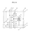
- FIG.16 is a circuit diagram showing a pixel circuit of a conventional movable shutter-type image display device.
- the conventional movable shutter-type image display device will be described with reference to FIG.16 .
- Each pixel circuit 213 includes a signal line 206.
- the signal line 206 and a signal storage capacitance 204 are connected to each other by a signal transfer switch 205.
- the signal storage capacitance 204 is also connected to a gate of an n-type MOS transistor 203 for shutter negative voltage write.
- a drain of the n-type MOS transistor 203 for shutter negative voltage write is connected to a drain of a p-type MOS transistor 202 for shutter positive voltage write via a cascode n-type MOS transistor 216 and a cascode p-type MOS transistor 215.
- Each pixel includes a dual actuator shutter assembly 201 connected to a shutter voltage line 211.
- One of two control electrodes of the dual actuator shutter assembly 201 is connected to the drain of the n-type MOS transistor 203 for shutter negative voltage write via the cascode n-type MOS transistor 216.
- the other control electrode is connected to a control electrode voltage line 209.
- the other end of the signal storage capacitance 204 is connected to the shutter voltage line 211.
- a source of the n-type MOS transistor 203 for shutter negative voltage write is connected to an nMOS source voltage line 212 for shutter negative voltage write.
- a gate and the drain of the p-type MOS transistor 202 for shutter positive voltage write are respectively connected to a pMOS gate voltage line 207 for shutter positive voltage write and a positive voltage line 208.
- a gate of the cascode n-type MOS transistor 216 and a gate of the cascode p-type MOS transistor 215 are connected to a cascode gate voltage line 217.
- a gate of the signal transfer switch 205 is connected to a scanning line 210.
- the dual actuator shutter assembly 201 is provided to face an opening in a light blocking surface.
- This image display device includes a plurality of such pixel circuits 213 arrayed in a matrix.
- An image signal voltage written to the signal line 206 is stored on the signal storage capacitance 204 via the signal transfer switch 205 by scanning the scanning lines 210 sequentially. Then, after the scanning operation for writing an image signal voltage on the signal storage capacitances 204 of all the pixels is finished, each pixel performs amplified write of an image signal to one of the control electrodes of the dual actuator shutter assembly 201, based on the written image signal voltage. Namely, in all the pixels, the pMOS gate voltage line 207 for shutter positive voltage write is put into a low voltage state for a prescribed time period, so that the p-type MOS transistor 202 for shutter positive voltage write is put into an ON state for this period.
- one of the control electrodes of the dual actuator shutter assembly 201 is precharged with a prescribed positive voltage, which has been applied to the positive voltage line 208.
- the nMOS source voltage line 212 for shutter negative voltage write is put into a low voltage state for a prescribed time period. For this period, only in a pixel which includes the signal storage capacitance 204 having a high voltage as an image signal voltage written therein, the n-type MOS transistor 203 for shutter negative voltage write is put into an ON state.
- the voltage of one of the control electrodes of the dual actuator shutter assembly 201 is re-rewritten with a prescribed low voltage applied to the nMOS source voltage line 212 for shutter negative voltage write.
- the n-type MOS transistor 203 for shutter negative voltage write is kept in an OFF state for the above-mentioned period. Therefore, the voltage of one of the control electrodes of the dual actuator shutter assembly 201 is kept in the state of being precharged at the prescribed positive voltage. In this manner, amplified write of an image signal is performed on one of the control electrodes of the dual actuator shutter assembly 201. In parallel with this, a voltage applied to the control electrode voltage line 209 is controlled, so that the dual actuator shutter assembly 201 can be electrostatically operated to be opened or closed.
- the opening provided in the light blocking surface of the dual actuator shutter assembly 201 is opened or closed in this manner, so that the amount of transmitted light is controlled.
- the image display device can display an image corresponding to the written image signal voltage on the pixel matrix.
- the cascode n-type MOS transistor 216 and the cascode p-type MOS transistor 215 are provided in order to protect the p-type MOS transistor 202 for shutter positive voltage write and the n-type MOS transistor 203 for shutter negative voltage write against write of a high drain voltage which may spoil the reliability life thereof.
- FIG.6 provides schematic views of a shutter electrode 20 and a control electrode 21 provided in each of pixels in a movable shutter-type image display device.
- An insulating film 50 of alumina or silicon nitride is provided around the electrodes.
- FIG.6(a) shows that the shutter electrode 20 is electrostatically attracted to the control electrode 21. A voltage of, for example, 25V is applied between the electrodes.
- a prescribed electric field is generated in the insulating film 50 located between the electrodes, and thus a leak current is generated due to Poole-Frankel or Fowler-Nordheim injection current.
- Which of the current injection mechanisms mainly acts is determined by the quality of the film, electric field, temperature or the like.
- the generated leak current is defined as electron injection directed from the shutter electrode 20 toward the control electrode 21.
- the insulating film 50 located between the electrodes has a contact interface and a great number of electron trap levels are existent around the contact interface.
- Electrons released from the insulating film 50 on the shutter electrode 20 side are concentrated in tiny convexed portions on the insulating film, and therefore the influence of the electron trap is small.
- injected electrons are dispersed in a large area of the interface of the insulating film 50, and therefore a great number of electrons are trapped at the electron trap levels. This is shown in FIG.6(b).
- FIG.6(c) shows a state where no voltage is applied between the electrodes after the state of FIG.6(b) . Even when there is no voltage applied anymore, electrons, once trapped, stay at the interface of the insulating film 50 for a relatively long period. Even when a negative electrode is kept applied to the shutter electrode 20 and a positive electrode is kept applied to the control electrode 21 in order to close the electrodes, the residual charges decrease the potential of the positive electrode. As a result, the control on the shutter performed by use of electrostatic attraction is destabilized. As a result, the life of the mechanical shutter or the life of the display device may be reduced.
- the present invention for solving these problems of the conventional art has an object of providing a technology capable of, in a movable shutter-type image display device, significantly decreasing the amount of trapped electrons (charges) caused by a leak current to alleviate the control fault of the mechanical shutter and thus to significantly extend the life of the display.
- the present invention is directed to a display device, comprising a plurality of pixels each including a mechanical shutter, the display device electrically controlling the position of the mechanical shutter to provide image display, wherein each of the pixels includes a pixel circuit for electrically controlling the position of the mechanical shutter; and the pixel circuit includes a first control electrode and a second control electrode provided as a pair with respect to the mechanical shutter; a first mean for applying a prescribed control voltage to the first control electrode and the second control electrode to put the mechanical shutter and the first control electrode or the second control electrode into contact with each other; and a second mean for, in a state where the mechanical shutter is at a stop, decreasing a potential difference between the mechanical shutter and the first control electrode or the second control electrode which is in contact with the mechanical shutter.
- the present invention is also directed to a display device, comprising a plurality of pixels each including a mechanical shutter, the display device electrically controlling the position of the mechanical shutter to provide image display, wherein each of the pixels includes a pixel circuit for electrically controlling the position of the mechanical shutter; and the pixel circuit includes a first control electrode and a second control electrode provided as a pair with respect to the mechanical shutter; a first mean for applying a prescribed control voltage to the first control electrode and the second control electrode to put the mechanical shutter and the first control electrode or the second control electrode into contact with each other; and a second mean for, in a state where the mechanical shutter is at a stop, decreasing a potential difference between the mechanical shutter and the second control electrode which is in contact with the mechanical shutter.
- FIG.1 is a circuit diagram showing a pixel circuit of a movable shutter-type image display device in Example 1 according to the present invention.
- a pixel circuit 23 in this example is a CMOS circuit, and includes p-type MOS transistors 2 and 14 connected between a power supply line 7 supplied with a VDD voltage and a power supply line 12 supplied with a GND voltage, and n-type MOS transistors 3 and 15.
- Each pixel circuit 23 includes a signal line 6, and the signal line 6 and a signal storage capacitance (hereinafter, referred to as a "storage capacitance") 4 are connected to each to other by a signal transfer switch (input transistor according to the present invention) 5, which is an n-type MOS transistor.
- the storage capacitance 4 is also connected to a source (or a drain) of a signal transfer switch (transfer transistor) according to the present invention) 13, which is an n-type MOS transistor.
- the drain (or the source) of the signal transfer switch 13 is connected to a gate of the p-type MOS transistor 2 and a gate of the n-type MOS transistor 3.
- the other end of the storage capacitance 4 is connected to the power supply line 12, and a gate of the signal transfer switch 5 is connected to an update line 8.
- the gate of the p-type MOS transistors 2 and the gate of the n-type MOS transistor 3 are connected to one of control electrodes 22 of a mechanical shutter, and a gate of the p-type MOS transistor 14 and a gate of the n-type MOS transistor 15 are connected to the other control electrode of the mechanical shutter.
- the shutter electrode 20 is connected to a shutter voltage line 11. As described later with reference to FIG.3 , the mechanical shutter is provided to face an opening in a light blocking surface.
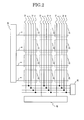
- FIG.2 is a block diagram showing a schematic structure of the movable shutter-type image display device in Example 1 according to the present invention.
- a plurality of the pixel circuits 23 shown in FIG.1 are arrayed two-dimensionally, and each pixel circuit 23 acts as a pixel.
- a scanning line 10 is provided for each row and is connected to a scanning circuit 25.
- the signal line 6 is provided for each column and is connected to an image signal voltage write circuit 24.
- the power supply lines 7 and 12, the update line 8, and the shutter voltage line 11 are provided commonly to the pixels, and are connected to a control electrode driving circuit 26.
- FIG.2 shows a display area as including the pixels in a matrix of 4 x 3 for the sake of simplicity, but obviously, the technological philosophy of the present invention does not specifically limit the number of pixels.
- FIG.3 is a cross-sectional view showing a cross-sectional structure of the pixel area of the movable shutter-type image display device in Example 1 according to the present invention.
- a polycrystalline silicon thin film transistor is provided on a glass substrate 39.
- the polycrystalline silicon thin film transistor includes a polycrystalline silicon thin film 31, polycrystalline silicon thin films 30 and 32 doped with a high concentration n-type impurity, a gate insulating film 33, and a gate electrode 35, a source electrode 37 and a drain electrode 36 which are formed of a high melting point metal material.
- a shutter voltage line 11 and a drain electrode 40 (e.g., drain of the n-type MOS transistor 15) which are formed of Al like the source electrode 37 and the drain electrode 36.
- a protective film 38 including a plurality of layers of silicon nitride and an organic material.
- a dual actuator shutter assembly 1 including the shutter electrode 20 and control electrodes 21 and 22 is provided on the protective film 38.
- the shutter electrode 20 is connected to the shutter voltage line 11, the drain electrode 36 is connected to the control electrode 22, and the drain electrode 40 is connected to the control electrode 21, via respective contact holes.
- the shutter electrode 20 and the two control electrodes 21 and 22 are covered with an insulating film so as not to be short-circuited when contacting each other.
- FIG.3 also shows the movable range of the shutter electrode 20.
- other transistors provided in the pixel circuit 23 are also polycrystalline silicon thin film transistors. These polycrystalline silicon thin film transistors can be produced by use of a known excimer laser annealing process or the like.
- a light guide plate 47 including a light source 42 is provided at a position facing the glass substrate 39 with the shutter electrode 20 located therebetween.
- the light source 42 includes independent LED light sources of three colors of R (red), G (green) and B (blue).
- the reflective films 46 and 48 are metal films of Ag, Al or the like.
- the black film 49 may be formed of a metal oxide film, a polyimide resin or the like which has pigment particles of carbon black, titanium black or the like dispersed therein appropriately.
- the reflective film 48 and the black film 49 have an opening at a position corresponding to the shutter electrode 20. A part of light 41 emitted from the light source 42 and propagated in the light guide plate 47 is output through the opening.
- the black film 49 is provided in order to prevent reflection of external light.
- FIG.4 and FIG.5 are each an operation timing diagram of the movable shutter-type image display device in this example according to the present invention.
- a shutter control voltage on the shutter voltage line (shutter line) 11 a scanning voltage on the scanning line (gate line) 10, a transfer control signal on the update line 8, and a power supply voltage on the power supply line (actuate line) 7
- the horizontal axis represents the time and the vertical axis represents the level of the voltage.
- FIG.4 and FIG.5 show the position of the shutter electrode 20 with respect to the control electrodes 21 and 22.
- the shutter voltage line 11 has a voltage of 0V in FIG.4 and has a high Vdrive voltage (e.g., 25V) in FIG.5 .
- the image display device in this example represents full-color 8-bit gradation by an opened/closed state of the shutter.
- PMW Pulse Width Modulation
- the light emission to the outside is controlled by opening or closing the shutter electrode 20.
- polarity inversion driving is performed at an interval of a prescribed number of sub frames in order to avoid deterioration of the electrodes of the mechanical shutter.
- the transfer control signal on the update line 8 becomes High (hereinafter, referred to as "H level”), and thus the signal transfer switch 13 is turned ON.
- H level the transfer control signal on the update line 8 becomes High
- L level Low
- the power supply voltage on the power supply line 7 is raised to a level of Vdrive (e.g., 25V), and thus the shutter electrode 20 is driven.
- Vdrive e.g. 25V
- the shutter electrode 20 is driven.
- the shutter electrode 20 is in contact with either the control electrode 21 or 22.
- the shutter electrode 20 is moved to an intermediate position.
- the shutter electrode 20 starts moving toward either the control electrode 21 or 22.
- the shutter electrode 20 is supplied with a voltage of 0V.
- the control electrode on a high voltage side is supplied with a Vdrive voltage (e.g., 25V), whereas the control electrode on a low voltage side is supplied with a voltage of 0V.
- the shutter control voltage on the shutter voltage line 11 becomes a level of Vrelease1 (e.g., 10V).
- Vrelease1 e.g. 10V
- the potential difference between the shutter electrode 20 and the control electrode on the high voltage side is decreased from 25V to 15V.
- the shutter electrode 20 is already at a stop. Therefore, there is no influence on the shutter characteristics even though the applied voltage is decreased.
- the transfer control signal on the update line 8 becomes H level, and thus the signal transfer switch 13 is turned ON.
- a signal is input to the SRAM circuit formed of the p-type MOS transistors 2 and 14 and the n-type MOS transistors 3 and 15.
- the power supply voltage of the power supply line 7 is raised to a level of Vlatch, and thus an image signal is latched by the SRAM circuit.
- the transfer control signal on the update line 8 becomes L level, and thus the signal transfer switch 13 is turned OFF.
- the power supply voltage on the power supply line 7 is raised to a level of Vdrive (e.g., 25V), and thus the shutter electrode 20 is driven.
- Vdrive e.g. 25V
- the shutter electrode 20 is in contact with either the control electrode 21 or 22.
- the shutter electrode 20 starts moving toward either the control electrode 21 or 22.
- the shutter electrode 20 is supplied with a Vdrive voltage (e.g., 25V).
- the control electrode on the high voltage side is supplied with a Vdrive voltage (e.g., 25V), whereas the control electrode on the low voltage side is supplied with a voltage of 0V.
- the shutter control voltage on the shutter voltage line 11 becomes a level of Vrelease2 (e.g., 15V).
- Vrelease2 e.g. 15V
- the potential difference between the shutter electrode 20 and the control electrode on the low voltage side is decreased from 25V to 15V.
- the shutter electrode 20 is already at a stop. Therefore, there is no influence on the shutter characteristics even though the applied voltage is decreased.
- the operation in FIG.5 is opposite to the operation in FIG.4 in the high/low relationship regarding the shutter control voltage on the shutter voltage line 11. For this reason, the operation of the shutter 20 is different, but the basic operating principle is the same.
- the potential difference between the voltages applied to the electrodes is 25V as by the conventional art. After the electrodes contact each other, the potential difference between the voltages applied to the electrodes is decreased to 15V.
- a leak current between the electrodes is in proportion to the voltage applied between the electrodes (Poole-Frankel injection current) or is an exponential function of the voltage applied between the electrodes (Fowler-Nordheim injection current). Therefore, the leak current heavily relies on the voltage. The leak current is generated after the electrodes contact each other.
- the control of the shutter electrode uses the potential difference of 25V. Therefore, even though the applied voltage is decreased, there is no influence on the shutter characteristics.
- the potential difference between the voltages applied to the electrodes is 25 V as by the conventional art. After the electrodes contact each other, the potential difference between the voltages applied to the electrodes is decreased to 15V. As long as the potential difference between the voltages applied to the electrodes is between 10V and 15V, substantially the same function and effect are provided.
- FIG.7 and FIG.8 are each an operation timing diagram of the movable shutter-type image display device in this example according to the present invention.
- FIG.7 and FIG.8 respectively correspond to FIG.4 and FIG.5 described above.
- the horizontal axis represents the time and the vertical axis represents the level of the voltage.
- FIG.7 and FIG.8 show the position of the shutter electrode 20 with respect to the control electrodes 21 and 22.
- the power supply voltage on the power supply line 7, instead of the shutter control voltage on the shutter voltage line 11, is varied to decrease the voltage applied to the control voltages 21 and 22 from the level of the Vdrive voltage to the level of Vrelease3.
- the shutter control voltage on the shutter voltage line 11 is 0V.
- the scanning line 10 is sequentially supplied with scanning voltages and an image signal is written in the storage capacitance 4.
- the power supply voltage on the power supply line 7 becomes from a level of Vrelease3 (e.g., 15V) to 0V.
- the transfer control signal on the update line 8 becomes H level, and thus the signal transfer switch 13 is turned ON. As a result, a signal is input to the SRAM circuit formed of the p-type MOS transistors 2 and 14 and the n-type MOS transistors 3 and 15.
- the power supply voltage on the power supply line 7 is raised to a level of Vlatch, and thus an image signal is latched by the SRAM circuit.
- the transfer control signal on the update line 8 becomes L level, and thus the signal transfer switch 13 is turned OFF.
- the power supply voltage on the power supply line 7 is raised to a level of Vdrive (e.g., 25V), and thus the shutter electrode 20 is driven. In an initial state, the shutter electrode 20 is in contact with either the control electrode 21 or 22. After time t1, as a result of the power supply voltage on the power supply line 7 becoming 0V, the shutter electrode 20 is moved to an intermediate position.
- the shutter electrode 20 starts moving toward either the control electrode 21 or 22.
- the shutter electrode 20 is supplied with a voltage of 0V.
- the control electrode on the high voltage side is supplied with a Vdrive voltage (e.g., 25V), whereas the control electrode on the low voltage side is supplied with a voltage of 0V.
- the power supply voltage on the power supply line 7 becomes a level of Vrelease3 (e.g., 15V).
- Vrelease3 e.g. 15V
- the shutter control voltage on the shutter voltage line 11 is at a level of Vdrive.
- the scanning line 10 is sequentially supplied with scanning voltages and an image signal is written in the storage capacitance 4.
- the power supply voltage on the power supply line 12 becomes from a level of Vrelease4 (e.g., 10V) to 0V
- the power supply voltage on the power supply line 7 becomes from a level of Vdrive (e.g., 25V) to 0V.
- the transfer control signal on the update line 8 becomes H level, and thus the signal transfer switch 13 is turned ON.
- a signal is input to the SRAM circuit formed of the p-type MOS transistors 2 and 14 and the n-type MOS transistors 3 and 15.
- the power supply voltage on the power supply line 7 is raised to a level of Vlatch, and thus an image signal is latched by the SRAM circuit.
- the transfer control signal on the update line 8 becomes L level, and thus the signal transfer switch 13 is turned OFF.
- the power supply voltage on the power supply line 7 is raised to a level of Vdrive (e.g., 25V), and thus the shutter electrode 20 is driven.
- Vdrive e.g. 25V
- the shutter electrode 20 is in contact with either the control electrode 21 or 22.
- the shutter electrode 20 starts moving toward either the control electrode 21 or 22.
- the shutter electrode 20 is supplied with a Vdrive voltage (e.g., 25V).
- the control electrode on the high voltage side is supplied with a Vdrive voltage (e.g., 25V), whereas the control electrode on the low voltage side is supplied with a voltage of 0V.
- the power supply voltage on the power supply line 12 becomes a level of Vrelease4 (e.g., 10V).
- Vrelease4 e.g. 10V
- the potential difference between the shutter electrode 20 and the control electrode on the low voltage side is decreased from 25V to 10V.
- the shutter electrode 20 is already at a stop. Therefore, there is no influence on the shutter characteristics even though the applied voltage is decreased.
- the shutter control voltage on the shutter voltage line 11 can be of two values as in the conventional art. This provides an advantage that the structure of the control line driving circuit 26 can be easily simplified.
- Example 3 the present invention is applied to the conventional movable shutter-type image display device shown in FIG.16 .
- FIG.9 is a circuit diagram showing a pixel circuit of a movable shutter-type image display device in this example, which is the same as the conventional pixel circuit of the movable shutter-type image display device shown in FIG.16 .
- reference numerals 52 and 65 each represent a p-type MOS transistor
- reference numerals 53 and 66 each represent an n-type MOS transistor
- reference numeral 54 represents a signal storage capacitance (hereinafter, referred to as a "storage capacitance")
- reference numeral 55 represents a signal transfer switch
- reference numeral 56 represents a signal line
- reference numeral 57 represents a pMOS gate voltage line (reset line according to the present invention)
- reference numeral 58 represents a positive voltage line
- reference numeral 59 represents a control electrode voltage line (control line according to the present invention)
- reference numeral 60 represents a scanning line
- reference numeral 61 represents a shutter voltage line
- reference numeral 62 represents an nMOS source voltage line
- reference numeral 63 represents a pixel circuit
- reference numeral 67 represents a cascode gate voltage line.
- FIG.10 is a block diagram showing a schematic structure of the movable shutter-type image display device in this example.
- an image signal voltage write circuit 24 is shown above the pixel circuits 63 arrayed in a matrix.
- a scanning circuit 25 is shown above the left of the pixel circuits 63.
- a control electrode driving circuit 76 is shown below the pixel circuits 63.
- a plurality of the pixel circuits 63 shown in FIG.9 are arrayed two-dimensionally, and each pixel circuit 63 acts as a pixel.
- a scanning line 60 is provided for each row and is connected to the scanning circuit 25.
- the signal line 56 is provided for each column and is connected to the image signal voltage write circuit 24.
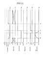
- FIG.11 and FIG.12 are each a timing diagram of the movable shutter-type image display device in this example according to the present invention.
- a shutter control voltage on the shutter voltage line (shutter line) 61 a scanning voltage on the scanning line (gate line) 60, a control voltage on the control electrode voltage line (global line) 59, a reset voltage on the pMOS gate voltage line (reset line) 57, a power supply voltage on the nMOS source voltage line (low line) 62, and a voltage to be applied to the control electrode 22,
- the horizontal axis represents the time and the vertical axis represents the level of the voltage.
- the shutter control voltage on the shutter voltage line 61 is 0V.
- the scanning line 60 is sequentially supplied with scanning voltages and an image signal is written in the storage capacitance 54.
- the shutter control voltage on the shutter voltage line 61 becomes from a level of Vrelease1 (e.g., 10V) to 0V.
- the control voltage on the control electrode voltage line 59 becomes from a level of Vdrive (e.g., 25V) to 0V.
- the reset voltage on the pMOS gate voltage line (reset line) 57 becomes from a level of Vdrive to 0V.
- the potential difference between the control electrode 21 and the shutter electrode 20 becomes 0V, and a Vdrive voltage is applied to the control electrode 22 via the p-type MOS transistor 52. Therefore, the shutter electrode 20 moves toward the control electrode 22.
- the positive voltage line 58 is always supplied with a Vdrive voltage.
- the reset voltage on the pMOS gate voltage line 57 becomes from 0V to a level of Vdrive
- the voltage on the nMOS source voltage line 62 becomes from a level of VM (e.g., 5V) to 0V.
- VM e.g., 5V
- the n-type MOS transistor 53 is turned ON, and a voltage of 0V is applied to the control electrode 22.
- the control electrode 22 is kept supplied with the Vdrive voltage.
- the control voltage on the control electrode voltage line 59 becomes from 0V to a level of Vdrive
- the voltage on the nMOS source voltage line 62 becomes from 0 V to a level of VM.
- the shutter control voltage on the shutter voltage line 61 becomes from 0V to a level of Vrelease1.
- the potential difference between the control electrode on the high voltage side and the shutter electrode 20 is decreased from 25V to 15V.
- the shutter electrode 20 is already at a stop. Therefore, there is no influence on the shutter characteristics even though the applied voltage is decreased.
- the shutter control voltage on the shutter voltage line 61 is at a level of Vdrive.
- the scanning line (gate line) 60 is sequentially supplied with scanning voltages and an image signal is written in the storage capacitance 54.
- the shutter control voltage on the shutter voltage line 61 becomes from a level of Vrelease2 (e.g., 15V) to a level of Vdrive (e.g., 25V).
- the control voltage on the control electrode voltage line (global line) 59 becomes from 0V to a level of Vdrive (e.g., 25V).
- the reset voltage on the pMOS gate voltage line (reset line) 57 becomes from a level of Vdrive to 0V.
- the potential difference between the control electrode 21 and the shutter electrode 20 becomes 0 V, and a Vdrive voltage is applied to the control electrode 22 via the p-type MOS transistor 52. Therefore, the shutter electrode 20 moves to an intermediate position.
- the reset voltage on the pMOS gate voltage line 57 becomes from 0V to a level of Vdrive, and the voltage on the nMOS source voltage line (low line) 62 becomes from a level of VM (e.g., 5V) to 0V.
- VM e.g., 5V
- the voltage on the nMOS source voltage line 62 becomes 0V
- the storage capacitance 54 stores an image signal of 5V
- the n-type MOS transistor 53 is turned ON, and a voltage of 0V is applied to the control electrode 22.
- the n-type MOS transistor 53 is not turned ON.
- the control electrode 22 is kept supplied with the Vdrive voltage.
- the shutter electrode 20 moves toward the control electrode 22.
- the control voltage on the control electrode voltage line 59 becomes from a level of Vdrive to 0V, and the voltage on the nMOS source voltage line 62 becomes from 0V to a level of VM.
- the shutter electrode 20 which has been moved to the intermediate position during the period from time t12 to time t13, moves toward the control electrode 21.
- the shutter control voltage on the shutter voltage line 61 becomes from a level of Vdrive to a level of Vrelease2.
- the potential difference between the shutter electrode 20 and the control electrode on the low voltage side is decreased from 25V to 15V.
- FIG.12 shows that the high/low relationship of the shutter control voltage on the shutter voltage line 61 and the control voltage on the control electrode voltage line 59 is opposite to each other, and the voltage applied to the control electrode 22 is different.
- the basic operating principle is the same.
- the timing at which the shutter electrode 20 operates is different between FIG.11 and FIG.12 , and the timing for obtaining a sufficient operation time is optimized. Therefore, in FIG.11 , the period between time 11 and time 12 is long; and in FIG.12 , the period between time 12 and time 13 is long.
- This example provides an advantage that the number of MOS transistors required in the pixel circuit 63 can be decreased.
- FIG.13 and FIG.14 are each a timing diagram of the movable shutter-type image display device in this example.
- FIG.13 and FIG.14 respectively correspond to FIG.11 and FIG.12 described above.
- the horizontal axis represents the time and the vertical axis represents the level of the voltage.
- the control voltage on the control electrode voltage line 59 instead of the shutter control voltage on the shutter voltage line 61, is decreased in the middle from a level of Vdrive to a level of Vrelease1 or a level of Vrelease2.
- the shutter control voltage on the shutter voltage line 61 is 0V.
- the scanning line 60 is sequentially supplied with scanning voltages and an image signal is written in the storage capacitance 54.
- the control voltage on the control electrode voltage line (global line) 59 becomes from a level of Vrelease2 (e.g., 15V) to 0V
- the reset voltage on the pMOS gate voltage line (reset line) 57 becomes from a level of Vdrive to 0V.
- the potential difference between the control electrode 21 and the shutter electrode 20 becomes 0V
- a Vdrive voltage is applied to the control electrode 22 via the p-type MOS transistor 52. Therefore, the shutter electrode 20 moves toward the control electrode 22.
- the reset voltage on the pMOS gate voltage line 57 becomes from 0V to a level of Vdrive, and the voltage on the nMOS source voltage line 62 becomes from a level of VM (e.g., 5V) to 0V.
- VM e.g., 5V
- the voltage on the nMOS source voltage line 62 becomes 0V
- the storage capacitance 54 stores an image signal of 5V
- the n-type MOS transistor 53 is turned ON, and a voltage of 0V is applied to the control electrode 22.
- the control electrode 22 is kept supplied with the Vdrive voltage.
- the control voltage on the control electrode voltage line 59 becomes from 0V to a level of Vdrive
- the voltage on the nMOS source voltage line 62 becomes from 0 V to a level of VM.
- the shutter control voltage on the shutter voltage line 61 becomes from 0V to a level of Vrelease2.
- the potential difference between the shutter electrode 20 and the control electrode 21 is decreased from 25V to 15V.
- the shutter electrode 20 is already at a stop. Therefore, there is no influence on the shutter characteristics even though the applied voltage is decreased.
- the shutter control voltage on the shutter voltage line (shutter line) 61 is at a level of Vdrive.
- the scanning line (gate line) 60 is sequentially supplied with scanning voltages and an image signal is written in the storage capacitance 54.
- the control voltage on the control electrode voltage line (global line) 59 becomes from a level of Vrelease1 (e.g., 10V) to a level of Vdrive (e.g., 25V), and the reset voltage on the pMOS gate voltage line (reset line) 57 becomes from a level of Vdrive to 0V.
- Vrelease1 e.g. 10V
- Vdrive e.g. 25V
- reset line pMOS gate voltage line
- the reset voltage on the pMOS gate voltage line 57 becomes from 0V to a level of Vdrive, and the voltage on the nMOS source voltage line (low line) 62 becomes from a level of VM (e.g., 5V) to 0V.
- VM e.g., 5V
- the voltage on the nMOS source voltage line 62 becomes 0V
- the storage capacitance 54 stores an image signal of 5 V
- the n-type MOS transistor 53 is turned ON, and a voltage of 0V is applied to the control electrode 22.
- the n-type MOS transistor 53 is not turned ON.
- the control electrode 22 is kept supplied with the Vdrive voltage.
- the shutter electrode 20 moves toward the control electrode 22.
- the control voltage on the control electrode voltage line 59 becomes from a level of Vdrive to 0 V, and the voltage on the nMOS source voltage line 62 becomes from 0 V to a level of VM.
- the shutter electrode 20 which has been moved to the intermediate position during the period from time t12 to time t13, moves toward the control electrode 21.
- the shutter control voltage on the shutter voltage line 61 becomes from a level of Vdrive to a level of Vrelease1.
- the potential difference between the shutter electrode 20 and the control electrode 21 is decreased from 25V to 15V.
- the shutter electrode 20 is already at a stop. Therefore, there is no influence on the shutter characteristics even though the applied voltage is decreased.
- the potential difference from the shutter electrode 20 is only the control electrode 21.
- the control electrode voltage line 59 drives the shutter electrode 20 with four values of voltage. This provides an advantage that the driving capacitance is small and thus the structure of the control electrode driving circuit 26 can be easily simplified.
- FIG.15 is a block diagram showing a schematic structure of an internet image display device 150 which uses a movable shutter-type image display device in Example 5 according to the present invention.
- I/F wireless interface
- An output of the wireless I/F circuit 152 is connected to a data bus 158 via an I/O (input/output) circuit 153.
- the data bus 158 is also connected to a microprocessor (MPU) 154, a display panel controller 156, a frame memory 157 and the like.
- MPU microprocessor
- An output of the display panel controller 156 is connected to a display device 151 which uses a mechanical shutter.
- the internet image display device 150 also includes a power supply 159.
- the display device 151 using the mechanical shutter has substantially the same structure as, and performs substantially the same operation as, those in Example 1 described above, and thus an internal structure and operation will thereof not be described.
- the wireless I/O circuit 152 receives compressed image data from outside in compliance with an instruction, and transfers the image data to the microprocessor 154 and the frame memory 157 via the I/O circuit 153.
- the microprocessor 154 drives the entirety of the internet image display device 150 when necessary to decode the compressed image data, process signals and display information.
- the image data processed here can be temporarily stored on the frame memory 157.
- the image data is input from the frame memory 157 to the display device 151 via the display panel controller 154 in compliance with the instruction.
- the display device 151 displays the input image data in real time.
- the display panel controller 156 also controls output of prescribed timing pulses required to display the image.
- the display device 151 uses these signals to display the input image data in real time.
- the power supply 159 includes a secondary cell, which supplies power for driving the entirety of the internet image display device 150.
- the internet image display device 150 capable of providing high quality display with small power consumption can be provided at low cost.
- the display device 151 as described in Example 1 is used as an image display device.
- any of various display devices described in other examples is usable. Needless to say, in such a case, the timing pulses output by the display panel controller 156 need to be changed slightly.
- n-type polycrystalline silicon thin film transistors are used.
- amorphous silicon thin film transistors which are obtained with no need of crystallization and thus can be produced by a low cost process, may be usable.
- the potential difference between the voltages applied to the electrodes is 25V as by the conventional art.
- the potential difference between the voltages applied to the electrodes is decreased to 15V. Owing to this, the amount of trapped electrons (charges) caused by a leak current can be decreased significantly.
- the control fault of the mechanical shutter can be alleviated, and the life of the display device can be extended significantly.
- the invention made by the present inventor has been described by way of examples. The present invention is not limited to the above-provided examples and may be modified in any of various manners without departing from the scope of the gist of the invention.
Landscapes
- Physics & Mathematics (AREA)
- Engineering & Computer Science (AREA)
- General Physics & Mathematics (AREA)
- Computer Hardware Design (AREA)
- Theoretical Computer Science (AREA)
- Optics & Photonics (AREA)
- Radar, Positioning & Navigation (AREA)
- Remote Sensing (AREA)
- Control Of Indicators Other Than Cathode Ray Tubes (AREA)
- Mechanical Light Control Or Optical Switches (AREA)
Abstract
Description
- This application is based upon and claims the benefit of priority from the prior Japanese Patent Application No.
2011-282643, filed on December 26, 2011 - The present invention relates to a display device and a method for driving the same, and specifically to a technology effectively applicable to a pixel circuit of an image display device for electrically controlling the position of a mechanical shutter to provide image display.
- A method of using an image display device for electrically controlling the position of a mechanical shutter to provide image display (hereinafter, referred to as a "movable shutter-type image display device") is described in
US 2008/0174532 .
FIG.16 is a circuit diagram showing a pixel circuit of a conventional movable shutter-type image display device.
Hereinafter, the conventional movable shutter-type image display device will be described with reference toFIG.16 .
Eachpixel circuit 213 includes asignal line 206. Thesignal line 206 and asignal storage capacitance 204 are connected to each other by asignal transfer switch 205.
Thesignal storage capacitance 204 is also connected to a gate of an n-type MOS transistor 203 for shutter negative voltage write. A drain of the n-type MOS transistor 203 for shutter negative voltage write is connected to a drain of a p-type MOS transistor 202 for shutter positive voltage write via a cascode n-type MOS transistor 216 and a cascode p-type MOS transistor 215.
Each pixel includes a dualactuator shutter assembly 201 connected to ashutter voltage line 211. One of two control electrodes of the dualactuator shutter assembly 201 is connected to the drain of the n-type MOS transistor 203 for shutter negative voltage write via the cascode n-type MOS transistor 216. The other control electrode is connected to a controlelectrode voltage line 209.
The other end of thesignal storage capacitance 204 is connected to theshutter voltage line 211. A source of the n-type MOS transistor 203 for shutter negative voltage write is connected to an nMOSsource voltage line 212 for shutter negative voltage write.
A gate and the drain of the p-type MOS transistor 202 for shutter positive voltage write are respectively connected to a pMOSgate voltage line 207 for shutter positive voltage write and apositive voltage line 208. A gate of the cascode n-type MOS transistor 216 and a gate of the cascode p-type MOS transistor 215 are connected to a cascodegate voltage line 217. A gate of thesignal transfer switch 205 is connected to ascanning line 210.
The dualactuator shutter assembly 201 is provided to face an opening in a light blocking surface. This image display device includes a plurality ofsuch pixel circuits 213 arrayed in a matrix. - Now, an operation of the conventional movable shutter-type image display device will be described.
An image signal voltage written to thesignal line 206 is stored on thesignal storage capacitance 204 via thesignal transfer switch 205 by scanning thescanning lines 210 sequentially.
Then, after the scanning operation for writing an image signal voltage on thesignal storage capacitances 204 of all the pixels is finished, each pixel performs amplified write of an image signal to one of the control electrodes of the dualactuator shutter assembly 201, based on the written image signal voltage. Namely, in all the pixels, the pMOSgate voltage line 207 for shutter positive voltage write is put into a low voltage state for a prescribed time period, so that the p-type MOS transistor 202 for shutter positive voltage write is put into an ON state for this period. Thus, one of the control electrodes of the dualactuator shutter assembly 201 is precharged with a prescribed positive voltage, which has been applied to thepositive voltage line 208.
Next, the nMOSsource voltage line 212 for shutter negative voltage write is put into a low voltage state for a prescribed time period. For this period, only in a pixel which includes thesignal storage capacitance 204 having a high voltage as an image signal voltage written therein, the n-type MOS transistor 203 for shutter negative voltage write is put into an ON state. As a result, the voltage of one of the control electrodes of the dualactuator shutter assembly 201 is re-rewritten with a prescribed low voltage applied to the nMOSsource voltage line 212 for shutter negative voltage write. - In a pixel which includes the
signal storage capacitance 204 having a low voltage as an image signal voltage written therein, the n-type MOS transistor 203 for shutter negative voltage write is kept in an OFF state for the above-mentioned period. Therefore, the voltage of one of the control electrodes of the dualactuator shutter assembly 201 is kept in the state of being precharged at the prescribed positive voltage.
In this manner, amplified write of an image signal is performed on one of the control electrodes of the dualactuator shutter assembly 201. In parallel with this, a voltage applied to the controlelectrode voltage line 209 is controlled, so that the dualactuator shutter assembly 201 can be electrostatically operated to be opened or closed. The opening provided in the light blocking surface of the dualactuator shutter assembly 201 is opened or closed in this manner, so that the amount of transmitted light is controlled. Thus, the image display device can display an image corresponding to the written image signal voltage on the pixel matrix.
In the above-described operation, the cascode n-type MOS transistor 216 and the cascode p-type MOS transistor 215 are provided in order to protect the p-type MOS transistor 202 for shutter positive voltage write and the n-type MOS transistor 203 for shutter negative voltage write against write of a high drain voltage which may spoil the reliability life thereof. - It was found that in a movable shutter-type image display device, a control fault of a mechanical shutter which reduces the life of the device is caused by an adhesive force caused between the shutter electrode and the control electrode.
This will be described with reference toFIG.6. FIG.6 provides schematic views of ashutter electrode 20 and acontrol electrode 21 provided in each of pixels in a movable shutter-type image display device. Aninsulating film 50 of alumina or silicon nitride is provided around the electrodes.
FIG.6(a) shows that theshutter electrode 20 is electrostatically attracted to thecontrol electrode 21. A voltage of, for example, 25V is applied between the electrodes. At this point, a prescribed electric field is generated in theinsulating film 50 located between the electrodes, and thus a leak current is generated due to Poole-Frankel or Fowler-Nordheim injection current.
Which of the current injection mechanisms mainly acts is determined by the quality of the film, electric field, temperature or the like. For example, in the case where theshutter electrode 20 is supplied with a negative voltage and thecontrol electrode 21 is supplied with a positive voltage, the generated leak current is defined as electron injection directed from theshutter electrode 20 toward thecontrol electrode 21. It should be noted that theinsulating film 50 located between the electrodes has a contact interface and a great number of electron trap levels are existent around the contact interface.
Electrons released from theinsulating film 50 on theshutter electrode 20 side are concentrated in tiny convexed portions on the insulating film, and therefore the influence of the electron trap is small. By contrast, on thecontrol electrode 21 side, injected electrons are dispersed in a large area of the interface of theinsulating film 50, and therefore a great number of electrons are trapped at the electron trap levels. This is shown inFIG.6(b). -
FIG.6(c) shows a state where no voltage is applied between the electrodes after the state ofFIG.6(b) . Even when there is no voltage applied anymore, electrons, once trapped, stay at the interface of theinsulating film 50 for a relatively long period. Even when a negative electrode is kept applied to theshutter electrode 20 and a positive electrode is kept applied to thecontrol electrode 21 in order to close the electrodes, the residual charges decrease the potential of the positive electrode. As a result, the control on the shutter performed by use of electrostatic attraction is destabilized. As a result, the life of the mechanical shutter or the life of the display device may be reduced.
The present invention for solving these problems of the conventional art has an object of providing a technology capable of, in a movable shutter-type image display device, significantly decreasing the amount of trapped electrons (charges) caused by a leak current to alleviate the control fault of the mechanical shutter and thus to significantly extend the life of the display.
The foregoing and the other objects and novel features of the present invention will be made clear by the description in this specification and the attached drawings. - Representative subject matter of the invention disclosed in this application is as follows.
In order to solve the above-described problems, the present invention is directed to a display device, comprising a plurality of pixels each including a mechanical shutter, the display device electrically controlling the position of the mechanical shutter to provide image display, wherein each of the pixels includes a pixel circuit for electrically controlling the position of the mechanical shutter; and the pixel circuit includes a first control electrode and a second control electrode provided as a pair with respect to the mechanical shutter; a first mean for applying a prescribed control voltage to the first control electrode and the second control electrode to put the mechanical shutter and the first control electrode or the second control electrode into contact with each other; and a second mean for, in a state where the mechanical shutter is at a stop, decreasing a potential difference between the mechanical shutter and the first control electrode or the second control electrode which is in contact with the mechanical shutter.
The present invention is also directed to a display device, comprising a plurality of pixels each including a mechanical shutter, the display device electrically controlling the position of the mechanical shutter to provide image display, wherein each of the pixels includes a pixel circuit for electrically controlling the position of the mechanical shutter; and the pixel circuit includes a first control electrode and a second control electrode provided as a pair with respect to the mechanical shutter; a first mean for applying a prescribed control voltage to the first control electrode and the second control electrode to put the mechanical shutter and the first control electrode or the second control electrode into contact with each other; and a second mean for, in a state where the mechanical shutter is at a stop, decreasing a potential difference between the mechanical shutter and the second control electrode which is in contact with the mechanical shutter. -
-
FIG.1 is a circuit diagram showing a pixel circuit of a movable shutter-type image display device in Example 1 according to the present invention. -
FIG.2 is a block diagram showing a schematic structure of the movable shutter-type image display device in Example 1 according to the present invention. -
FIG.3 is a cross-sectional view showing a cross-sectional structure of a pixel area of the movable shutter-type image display device in Example 1 according to the present invention. -
FIG.4 is an operation timing diagram of the movable shutter-type image display device in Example 1 according to the present invention (polarity inversion: shutter = low voltage). -
FIG.5 is an operation timing diagram of the movable shutter-type image display device in Example 1 according to the present invention (polarity inversion: shutter = high voltage). -
FIG.6 is a schematic view of a shutter electrode and a control electrode provided in each of pixels of a movable shutter-type image display device. -
FIG.7 is an operation timing diagram of a movable shutter-type image display device in Example 2 according to the present invention (polarity inversion: shutter = low voltage). -
FIG.8 is an operation timing diagram of the movable shutter-type image display device in Example 2 according to the present invention (polarity inversion: shutter = high voltage). -
FIG.9 is a circuit diagram showing a pixel circuit of a movable shutter-type image display device in Example 3 according to the present invention. -
FIG.10 is a block diagram showing a schematic structure of the movable shutter-type image display device in Example 3 according to the present invention. -
FIG.11 is an operation timing diagram of the movable shutter-type image display device in Example 3 according to the present invention (polarity inversion: shutter = low voltage). -
FIG.12 is an operation timing diagram of the movable shutter-type image display device in Example 3 according to the present invention (polarity inversion: shutter = high voltage). -
FIG.13 is an operation timing diagram of a movable shutter-type image display device in Example 4 according to the present invention (polarity inversion: shutter = low voltage). -
FIG.14 is an operation timing diagram of the movable shutter-type image display device in Example 4 according to the present invention (polarity inversion: shutter = high voltage). -
FIG.15 is a block diagram showing a schematic structure of an internet image display device using a movable shutter-type image display device in Example 5 according to the present invention. -
FIG.16 is a circuit diagram showing a pixel circuit of a conventional movable shutter-type image display device. - Hereinafter, examples of the present invention will be described with reference to the drawings.
In the drawings provided to explain the examples, elements having identical functions will bear identical reference numerals, and the same descriptions will be omitted. The following examples do not limit the scope or interpretation of the claims of the present invention. -
FIG.1 is a circuit diagram showing a pixel circuit of a movable shutter-type image display device in Example 1 according to the present invention.
Apixel circuit 23 in this example is a CMOS circuit, and includes p-type MOS transistors power supply line 7 supplied with a VDD voltage and apower supply line 12 supplied with a GND voltage, and n-type MOS transistors
Eachpixel circuit 23 includes asignal line 6, and thesignal line 6 and a signal storage capacitance (hereinafter, referred to as a "storage capacitance") 4 are connected to each to other by a signal transfer switch (input transistor according to the present invention) 5, which is an n-type MOS transistor.
Thestorage capacitance 4 is also connected to a source (or a drain) of a signal transfer switch (transfer transistor) according to the present invention) 13, which is an n-type MOS transistor. The drain (or the source) of thesignal transfer switch 13 is connected to a gate of the p-type MOS transistor 2 and a gate of the n-type MOS transistor 3. The other end of thestorage capacitance 4 is connected to thepower supply line 12, and a gate of thesignal transfer switch 5 is connected to anupdate line 8.
The gate of the p-type MOS transistors 2 and the gate of the n-type MOS transistor 3 are connected to one ofcontrol electrodes 22 of a mechanical shutter, and a gate of the p-type MOS transistor 14 and a gate of the n-type MOS transistor 15 are connected to the other control electrode of the mechanical shutter. Theshutter electrode 20 is connected to ashutter voltage line 11.
As described later with reference toFIG.3 , the mechanical shutter is provided to face an opening in a light blocking surface. -
FIG.2 is a block diagram showing a schematic structure of the movable shutter-type image display device in Example 1 according to the present invention.
In the movable shutter-type image display device shown inFIG.2 , a plurality of thepixel circuits 23 shown inFIG.1 are arrayed two-dimensionally, and eachpixel circuit 23 acts as a pixel. Ascanning line 10 is provided for each row and is connected to ascanning circuit 25.
Thesignal line 6 is provided for each column and is connected to an image signalvoltage write circuit 24. Thepower supply lines update line 8, and theshutter voltage line 11 are provided commonly to the pixels, and are connected to a controlelectrode driving circuit 26.
FIG.2 shows a display area as including the pixels in a matrix of 4 x 3 for the sake of simplicity, but obviously, the technological philosophy of the present invention does not specifically limit the number of pixels. - Now, a cross-sectional structure of a pixel area of the movable shutter-type image display device in this example will be described.
FIG.3 is a cross-sectional view showing a cross-sectional structure of the pixel area of the movable shutter-type image display device in Example 1 according to the present invention.
As shown inFIG.3 , a polycrystalline silicon thin film transistor is provided on aglass substrate 39. The polycrystalline silicon thin film transistor includes a polycrystalline siliconthin film 31, polycrystalline siliconthin films gate insulating film 33, and agate electrode 35, asource electrode 37 and adrain electrode 36 which are formed of a high melting point metal material.
The following elements are further provided on theglass substrate 39 while an insulatingprotective film 34 is held between the above-mentioned elements and the following elements: ashutter voltage line 11 and a drain electrode 40 (e.g., drain of the n-type MOS transistor 15) which are formed of Al like thesource electrode 37 and thedrain electrode 36. These elements are covered with aprotective film 38 including a plurality of layers of silicon nitride and an organic material.
On theprotective film 38, a dualactuator shutter assembly 1 including theshutter electrode 20 andcontrol electrodes shutter electrode 20 is connected to theshutter voltage line 11, thedrain electrode 36 is connected to thecontrol electrode 22, and thedrain electrode 40 is connected to thecontrol electrode 21, via respective contact holes. Theshutter electrode 20 and the twocontrol electrodes - The position of the
shutter electrode 20 is controlled by an electric field which is varied by the relationship between the voltage applied to theshutter electrode 20 and the voltage applied to thecontrol electrodes FIG.3 also shows the movable range of theshutter electrode 20.
Although not shown inFIG.3 , other transistors provided in thepixel circuit 23 are also polycrystalline silicon thin film transistors. These polycrystalline silicon thin film transistors can be produced by use of a known excimer laser annealing process or the like.
At a position facing theglass substrate 39 with theshutter electrode 20 located therebetween, alight guide plate 47 including alight source 42 is provided. Thelight source 42 includes independent LED light sources of three colors of R (red), G (green) and B (blue).
On both of two surfaces of thelight guide plate 47,reflective films black film 49 is provided on thereflective film 48. Thereflective films black film 49 may be formed of a metal oxide film, a polyimide resin or the like which has pigment particles of carbon black, titanium black or the like dispersed therein appropriately.
As shown inFIG.3 , thereflective film 48 and theblack film 49 have an opening at a position corresponding to theshutter electrode 20. A part of light 41 emitted from thelight source 42 and propagated in thelight guide plate 47 is output through the opening. Theblack film 49 is provided in order to prevent reflection of external light. - Now, with reference to
FIG.4 andFIG.5 , an operation of the movable shutter-type image display device in this example will be described.
FIG.4 andFIG.5 are each an operation timing diagram of the movable shutter-type image display device in this example according to the present invention. InFIG.4 andFIG.5 , regarding a shutter control voltage on the shutter voltage line (shutter line) 11, a scanning voltage on the scanning line (gate line) 10, a transfer control signal on theupdate line 8, and a power supply voltage on the power supply line (actuate line) 7, the horizontal axis represents the time and the vertical axis represents the level of the voltage. Regarding theshutter electrode 20 at the bottom,FIG.4 andFIG.5 show the position of theshutter electrode 20 with respect to thecontrol electrodes
Theshutter voltage line 11 has a voltage of 0V inFIG.4 and has a high Vdrive voltage (e.g., 25V) inFIG.5 . This corresponds to an inversion (polarity inversion) operation of the driving voltage of the mechanical shutter.
The image display device in this example represents full-color 8-bit gradation by an opened/closed state of the shutter. For realizing this, the following PMW (Pulse Width Modulation) driving is performed. One frame is divided into at least 24 (= 8 x RGB) frames, and light emission from thelight source 42 is time-weighted for each sub frame. The light emission to the outside is controlled by opening or closing theshutter electrode 20. During the driving, polarity inversion driving is performed at an interval of a prescribed number of sub frames in order to avoid deterioration of the electrodes of the mechanical shutter. - First, with reference to
FIG.4 , an operation of the pixel circuit of the movable shutter-type image display device in this example in the state of "polarity inversion: shutter = low voltage" will be described.
Until time t1, thescanning line 10 is sequentially supplied with scanning voltages and an image signal is written in thestorage capacitance 4.
Next, at time t1, the power supply voltage on thepower supply line 7 becomes from a level of Vdrive (e.g., 25V) to 0V, and the shutter control voltage on theshutter voltage line 11 becomes from a level of Vrelease1 (e.g., 10V) to 0V.
Next, at time t2, the transfer control signal on theupdate line 8 becomes High (hereinafter, referred to as "H level"), and thus thesignal transfer switch 13 is turned ON. As a result, a signal is input to an SRAM circuit formed of the p-type MOS transistors type MOS transistors
At time t3, the power supply voltage of thepower supply line 7 is raised to a level of Vlatch, and thus an image signal is latched by the SRAM circuit.
Then, at time t4, the transfer control signal on theupdate line 8 becomes Low (hereinafter, referred to as "L level"), and thus thesignal transfer switch 13 is turned OFF. - At time t5, the power supply voltage on the
power supply line 7 is raised to a level of Vdrive (e.g., 25V), and thus theshutter electrode 20 is driven.
In an initial state, theshutter electrode 20 is in contact with either thecontrol electrode power supply line 7 becoming 0V, theshutter electrode 20 is moved to an intermediate position. Then, at time t5, theshutter electrode 20 starts moving toward either thecontrol electrode shutter electrode 20 is supplied with a voltage of 0V. The control electrode on a high voltage side is supplied with a Vdrive voltage (e.g., 25V), whereas the control electrode on a low voltage side is supplied with a voltage of 0V.
Then, at time t6, at the timing when theshutter electrode 20 stops moving, the shutter control voltage on theshutter voltage line 11 becomes a level of Vrelease1 (e.g., 10V). As a result, the potential difference between theshutter electrode 20 and the control electrode on the high voltage side is decreased from 25V to 15V. At this point, theshutter electrode 20 is already at a stop. Therefore, there is no influence on the shutter characteristics even though the applied voltage is decreased. - Now, with reference to
FIG.5 , an operation of the pixel circuit of the movable shutter-type image display device in this example in the state of "polarity inversion: shutter = high voltage" will be described.
Until time t1, thescanning line 10 is sequentially supplied with scanning voltages and an image signal is written in thestorage capacitance 4.
Next, at time t1, the power supply voltage on thepower supply line 7 becomes from a level of Vdrive (e.g., 25V) to 0V, and the shutter control voltage on theshutter voltage line 11 becomes from a level of Vrelease2 (e.g., 15V) to a level of Vdrive (e.g., 25V).
Next, at time t2, the transfer control signal on theupdate line 8 becomes H level, and thus thesignal transfer switch 13 is turned ON. As a result, a signal is input to the SRAM circuit formed of the p-type MOS transistors type MOS transistors
At time t3, the power supply voltage of thepower supply line 7 is raised to a level of Vlatch, and thus an image signal is latched by the SRAM circuit.
Then, at time t4, the transfer control signal on theupdate line 8 becomes L level, and thus thesignal transfer switch 13 is turned OFF. - At time t5, the power supply voltage on the
power supply line 7 is raised to a level of Vdrive (e.g., 25V), and thus theshutter electrode 20 is driven.
In an initial state, theshutter electrode 20 is in contact with either thecontrol electrode shutter electrode 20 starts moving toward either thecontrol electrode shutter electrode 20 is supplied with a Vdrive voltage (e.g., 25V). The control electrode on the high voltage side is supplied with a Vdrive voltage (e.g., 25V), whereas the control electrode on the low voltage side is supplied with a voltage of 0V.
Then, at time t6, at the timing when theshutter electrode 20 stops moving, the shutter control voltage on theshutter voltage line 11 becomes a level of Vrelease2 (e.g., 15V). As a result, the potential difference between theshutter electrode 20 and the control electrode on the low voltage side is decreased from 25V to 15V. At this point, theshutter electrode 20 is already at a stop. Therefore, there is no influence on the shutter characteristics even though the applied voltage is decreased.
The operation inFIG.5 is opposite to the operation inFIG.4 in the high/low relationship regarding the shutter control voltage on theshutter voltage line 11. For this reason, the operation of theshutter 20 is different, but the basic operating principle is the same. - As described above, in this example, until the
shutter electrode 20 contacts either thecontrol electrode
A leak current between the electrodes is in proportion to the voltage applied between the electrodes (Poole-Frankel injection current) or is an exponential function of the voltage applied between the electrodes (Fowler-Nordheim injection current). Therefore, the leak current heavily relies on the voltage.
The leak current is generated after the electrodes contact each other. By decreasing the potential difference between the voltages applied to the electrodes from 25V to 15V after the electrodes contact each other, the amount of trapped electrons (charges) caused by the leak current can be decreased significantly. As a result, the control fault of the mechanical shutter can be alleviated, and the life of the display device can be extended significantly.
The control of the shutter electrode (operation of moving the shutter electrode toward thecontrol electrode 21 or toward the control electrode 22) uses the potential difference of 25V. Therefore, even though the applied voltage is decreased, there is no influence on the shutter characteristics.
In the above description, until theshutter electrode 20 contacts either thecontrol electrode - A movable shutter-type image display device and a pixel circuit in this example have substantially the same structure as that in Example 1 described above, and will not be described again.
FIG.7 andFIG.8 are each an operation timing diagram of the movable shutter-type image display device in this example according to the present invention.FIG.7 andFIG.8 respectively correspond toFIG.4 andFIG.5 described above. InFIG.7 andFIG.8 , regarding the shutter control voltage on the shutter voltage line (shutter line) 11, the power supply on the power supply line (low line) 12, the scanning voltage on the scanning line (gate line) 10, the transfer control signal on theupdate line 8, and the power supply voltage on the power supply line (actuate line) 7, the horizontal axis represents the time and the vertical axis represents the level of the voltage. Regarding theshutter electrode 20 at the bottom,FIG.7 andFIG.8 show the position of theshutter electrode 20 with respect to thecontrol electrodes
In this example, the power supply voltage on thepower supply line 7, instead of the shutter control voltage on theshutter voltage line 11, is varied to decrease the voltage applied to thecontrol voltages
First, with reference toFIG.7 , an operation of the pixel circuit of the movable shutter-type image display device in this example in the state of "polarity inversion: shutter = low voltage" will be described. InFIG.7 , the shutter control voltage on theshutter voltage line 11 is 0V.
Until time t1, thescanning line 10 is sequentially supplied with scanning voltages and an image signal is written in thestorage capacitance 4.
Next, at time t1, the power supply voltage on thepower supply line 7 becomes from a level of Vrelease3 (e.g., 15V) to 0V.
Next, at time t2, the transfer control signal on theupdate line 8 becomes H level, and thus thesignal transfer switch 13 is turned ON. As a result, a signal is input to the SRAM circuit formed of the p-type MOS transistors type MOS transistors - At time t3, the power supply voltage on the
power supply line 7 is raised to a level of Vlatch, and thus an image signal is latched by the SRAM circuit.
Then, at time t4, the transfer control signal on theupdate line 8 becomes L level, and thus thesignal transfer switch 13 is turned OFF.
At time t5, the power supply voltage on thepower supply line 7 is raised to a level of Vdrive (e.g., 25V), and thus theshutter electrode 20 is driven.
In an initial state, theshutter electrode 20 is in contact with either thecontrol electrode power supply line 7 becoming 0V, theshutter electrode 20 is moved to an intermediate position. Then, at time t5, theshutter electrode 20 starts moving toward either thecontrol electrode shutter electrode 20 is supplied with a voltage of 0V. The control electrode on the high voltage side is supplied with a Vdrive voltage (e.g., 25V), whereas the control electrode on the low voltage side is supplied with a voltage of 0V.
Then, at time t6, at the timing when theshutter electrode 20 stops moving, the power supply voltage on thepower supply line 7 becomes a level of Vrelease3 (e.g., 15V). As a result, the potential difference between theshutter electrode 20 and the control electrode on the high voltage side is decreased from 25V to 15V. At this point, theshutter electrode 20 is already at a stop. Therefore, there is no influence on the shutter characteristics even though the applied voltage is decreased. - Now, with reference to
FIG.8 , an operation of the pixel circuit of the movable shutter-type image display device in this example in the state of "polarity inversion: shutter = high voltage" will be described. InFIG.8 , the shutter control voltage on theshutter voltage line 11 is at a level of Vdrive.
Until time t1, thescanning line 10 is sequentially supplied with scanning voltages and an image signal is written in thestorage capacitance 4.
Next, at time t1, the power supply voltage on thepower supply line 12 becomes from a level of Vrelease4 (e.g., 10V) to 0V, and the power supply voltage on thepower supply line 7 becomes from a level of Vdrive (e.g., 25V) to 0V.
Next, at time t2, the transfer control signal on theupdate line 8 becomes H level, and thus thesignal transfer switch 13 is turned ON. As a result, a signal is input to the SRAM circuit formed of the p-type MOS transistors type MOS transistors
At time t3, the power supply voltage on thepower supply line 7 is raised to a level of Vlatch, and thus an image signal is latched by the SRAM circuit.
Then, at time t4, the transfer control signal on theupdate line 8 becomes L level, and thus thesignal transfer switch 13 is turned OFF. - At time t5, the power supply voltage on the
power supply line 7 is raised to a level of Vdrive (e.g., 25V), and thus theshutter electrode 20 is driven.
In an initial state, theshutter electrode 20 is in contact with either thecontrol electrode shutter electrode 20 starts moving toward either thecontrol electrode shutter electrode 20 is supplied with a Vdrive voltage (e.g., 25V). The control electrode on the high voltage side is supplied with a Vdrive voltage (e.g., 25V), whereas the control electrode on the low voltage side is supplied with a voltage of 0V.
Then, at time t6, at the timing when theshutter electrode 20 stops moving, the power supply voltage on thepower supply line 12 becomes a level of Vrelease4 (e.g., 10V). As a result, the potential difference between theshutter electrode 20 and the control electrode on the low voltage side is decreased from 25V to 10V. At this point, theshutter electrode 20 is already at a stop. Therefore, there is no influence on the shutter characteristics even though the applied voltage is decreased.
In this example, the shutter control voltage on theshutter voltage line 11 can be of two values as in the conventional art. This provides an advantage that the structure of the controlline driving circuit 26 can be easily simplified. - In Example 3 according to the present invention, the present invention is applied to the conventional movable shutter-type image display device shown in
FIG.16 .
FIG.9 is a circuit diagram showing a pixel circuit of a movable shutter-type image display device in this example, which is the same as the conventional pixel circuit of the movable shutter-type image display device shown inFIG.16 .
InFIG.9 ,reference numerals reference numerals reference numeral 54 represents a signal storage capacitance (hereinafter, referred to as a "storage capacitance"),reference numeral 55 represents a signal transfer switch,reference numeral 56 represents a signal line,reference numeral 57 represents a pMOS gate voltage line (reset line according to the present invention),reference numeral 58 represents a positive voltage line,reference numeral 59 represents a control electrode voltage line (control line according to the present invention),reference numeral 60 represents a scanning line,reference numeral 61 represents a shutter voltage line,reference numeral 62 represents an nMOS source voltage line,reference numeral 63 represents a pixel circuit, andreference numeral 67 represents a cascode gate voltage line.
FIG.10 is a block diagram showing a schematic structure of the movable shutter-type image display device in this example.
Above thepixel circuits 63 arrayed in a matrix, an image signalvoltage write circuit 24 is shown. To the left of thepixel circuits 63, ascanning circuit 25 is shown. Below thepixel circuits 63, a controlelectrode driving circuit 76 is shown.
In the movable shutter-type image display device shown inFIG.10 , a plurality of thepixel circuits 63 shown inFIG.9 are arrayed two-dimensionally, and eachpixel circuit 63 acts as a pixel. Ascanning line 60 is provided for each row and is connected to thescanning circuit 25.
Thesignal line 56 is provided for each column and is connected to the image signalvoltage write circuit 24. The pMOSgate voltage line 57, thepositive voltage line 58, the controlelectrode voltage line 59, theshutter voltage line 61, the nMOSsource voltage line 62, and the cascodegate voltage line 67 are provided commonly to the pixels, and are connected to a controlelectrode driving circuit 76.
FIG.11 andFIG.12 are each a timing diagram of the movable shutter-type image display device in this example according to the present invention. InFIG.11 andFIG.12 , regarding a shutter control voltage on the shutter voltage line (shutter line) 61, a scanning voltage on the scanning line (gate line) 60, a control voltage on the control electrode voltage line (global line) 59, a reset voltage on the pMOS gate voltage line (reset line) 57, a power supply voltage on the nMOS source voltage line (low line) 62, and a voltage to be applied to thecontrol electrode 22, the horizontal axis represents the time and the vertical axis represents the level of the voltage. - First, with reference to
FIG.11 , an operation of the pixel circuit of the movable shutter-type image display device in this example in the state of "polarity inversion: shutter = low voltage" will be described. InFIG.11 , the shutter control voltage on theshutter voltage line 61 is 0V.
Until time t11, thescanning line 60 is sequentially supplied with scanning voltages and an image signal is written in thestorage capacitance 54.
Next, at time t11, the shutter control voltage on theshutter voltage line 61 becomes from a level of Vrelease1 (e.g., 10V) to 0V. The control voltage on the controlelectrode voltage line 59 becomes from a level of Vdrive (e.g., 25V) to 0V. The reset voltage on the pMOS gate voltage line (reset line) 57 becomes from a level of Vdrive to 0V.
As a result, the potential difference between thecontrol electrode 21 and theshutter electrode 20 becomes 0V, and a Vdrive voltage is applied to thecontrol electrode 22 via the p-type MOS transistor 52. Therefore, theshutter electrode 20 moves toward thecontrol electrode 22. Thepositive voltage line 58 is always supplied with a Vdrive voltage. - Next, at time t12, the reset voltage on the pMOS
gate voltage line 57 becomes from 0V to a level of Vdrive, and the voltage on the nMOSsource voltage line 62 becomes from a level of VM (e.g., 5V) to 0V.
When the voltage on the nMOSsource voltage line 62 becomes 0V, in the case where thestorage capacitance 54 stores an image signal of 5V, the n-type MOS transistor 53 is turned ON, and a voltage of 0V is applied to thecontrol electrode 22. In the case where thestorage capacitance 54 stores an image signal of 0V, the n-type MOS transistor 53 is not turned ON. Thus, thecontrol electrode 22 is kept supplied with the Vdrive voltage.
When the n-type MOS transistor 53 is turned ON and a voltage of 0V is applied to thecontrol electrode 22, theshutter electrode 20, which has been moved toward thecontrol electrode 22, moves to an intermediate position.
At time t13, the control voltage on the controlelectrode voltage line 59 becomes from 0V to a level of Vdrive, and the voltage on the nMOSsource voltage line 62 becomes from 0 V to a level of VM.
When the control voltage on the controlelectrode voltage line 59 becomes the level of Vdrive at time t13, theshutter electrode 20, which has been moved to the intermediate position during the period from time t12 to time t13, moves toward thecontrol electrode 21.
Then, at time t14, at the timing when theshutter electrode 20 stops moving, the shutter control voltage on theshutter voltage line 61 becomes from 0V to a level of Vrelease1. As a result, the potential difference between the control electrode on the high voltage side and theshutter electrode 20 is decreased from 25V to 15V. At this point, theshutter electrode 20 is already at a stop. Therefore, there is no influence on the shutter characteristics even though the applied voltage is decreased. - Now, with reference to
FIG.12 , an operation of the pixel circuit of the movable shutter-type image display device in this example in the state of "polarity inversion: shutter = high voltage" will be described. InFIG.12 , the shutter control voltage on theshutter voltage line 61 is at a level of Vdrive.
Until time t11, the scanning line (gate line) 60 is sequentially supplied with scanning voltages and an image signal is written in thestorage capacitance 54.
Next, at time t11, the shutter control voltage on theshutter voltage line 61 becomes from a level of Vrelease2 (e.g., 15V) to a level of Vdrive (e.g., 25V). The control voltage on the control electrode voltage line (global line) 59 becomes from 0V to a level of Vdrive (e.g., 25V). The reset voltage on the pMOS gate voltage line (reset line) 57 becomes from a level of Vdrive to 0V.
As a result, the potential difference between thecontrol electrode 21 and theshutter electrode 20 becomes 0 V, and a Vdrive voltage is applied to thecontrol electrode 22 via the p-type MOS transistor 52. Therefore, theshutter electrode 20 moves to an intermediate position.
At time t12, the reset voltage on the pMOSgate voltage line 57 becomes from 0V to a level of Vdrive, and the voltage on the nMOS source voltage line (low line) 62 becomes from a level of VM (e.g., 5V) to 0V.
When the voltage on the nMOSsource voltage line 62 becomes 0V, in the case where thestorage capacitance 54 stores an image signal of 5V, the n-type MOS transistor 53 is turned ON, and a voltage of 0V is applied to thecontrol electrode 22. In the case where thestorage capacitance 54 stores an image signal of 0V, the n-type MOS transistor 53 is not turned ON. Thus, thecontrol electrode 22 is kept supplied with the Vdrive voltage.
When the n-type MOS transistor 53 is turned ON and a voltage of 0 V is applied to thecontrol electrode 22, theshutter electrode 20 moves toward thecontrol electrode 22. - At time t13, the control voltage on the control
electrode voltage line 59 becomes from a level of Vdrive to 0V, and the voltage on the nMOSsource voltage line 62 becomes from 0V to a level of VM.
When the control voltage on the controlelectrode voltage line 59 becomes 0V at time t13, theshutter electrode 20, which has been moved to the intermediate position during the period from time t12 to time t13, moves toward thecontrol electrode 21.
Then, at time t14, at the timing when theshutter electrode 20 stops moving, the shutter control voltage on theshutter voltage line 61 becomes from a level of Vdrive to a level of Vrelease2. As a result, the potential difference between theshutter electrode 20 and the control electrode on the low voltage side is decreased from 25V to 15V. At this point, theshutter electrode 20 is already at a stop. Therefore, there is no influence on the shutter characteristics even though the applied voltage is decreased.
A comparison between the timing diagram ofFIG.12 and timing diagram ofFIG.11 shows that the high/low relationship of the shutter control voltage on theshutter voltage line 61 and the control voltage on the controlelectrode voltage line 59 is opposite to each other, and the voltage applied to thecontrol electrode 22 is different. However, the basic operating principle is the same.
The timing at which theshutter electrode 20 operates is different betweenFIG.11 andFIG.12 , and the timing for obtaining a sufficient operation time is optimized. Therefore, inFIG.11 , the period betweentime 11 andtime 12 is long; and inFIG.12 , the period betweentime 12 andtime 13 is long.
This example provides an advantage that the number of MOS transistors required in thepixel circuit 63 can be decreased. - A movable shutter-type image display device and a pixel circuit in this example have substantially the same structure as that in Example 3 described above, and will not be described again.
FIG.13 andFIG.14 are each a timing diagram of the movable shutter-type image display device in this example.FIG.13 andFIG.14 respectively correspond toFIG.11 andFIG.12 described above. InFIG.13 andFIG.14 , regarding the shutter control voltage on the shutter voltage line (shutter line) 61, the scanning voltage on the scanning line (gate line) 60, the control signal on the control electrode voltage line (global line) 59, the reset voltage on the pMOS gate voltage line (reset line) 57, the power supply voltage on the nMOS source voltage line (low line) 62, and the voltage to be applied to thecontrol electrode 22, the horizontal axis represents the time and the vertical axis represents the level of the voltage.
InFIG.13 andFIG.14 , the control voltage on the controlelectrode voltage line 59, instead of the shutter control voltage on theshutter voltage line 61, is decreased in the middle from a level of Vdrive to a level of Vrelease1 or a level of Vrelease2.
First, with reference toFIG.13 , an operation of the pixel circuit of the movable shutter-type image display device in this example in the state of "polarity inversion: shutter = low voltage" will be described. InFIG.13 , the shutter control voltage on theshutter voltage line 61 is 0V.
Until time t11, thescanning line 60 is sequentially supplied with scanning voltages and an image signal is written in thestorage capacitance 54.
Next, at time t11, the control voltage on the control electrode voltage line (global line) 59 becomes from a level of Vrelease2 (e.g., 15V) to 0V, and the reset voltage on the pMOS gate voltage line (reset line) 57 becomes from a level of Vdrive to 0V.
As a result, the potential difference between thecontrol electrode 21 and theshutter electrode 20 becomes 0V, and a Vdrive voltage is applied to thecontrol electrode 22 via the p-type MOS transistor 52. Therefore, theshutter electrode 20 moves toward thecontrol electrode 22. - At time t12, the reset voltage on the pMOS
gate voltage line 57 becomes from 0V to a level of Vdrive, and the voltage on the nMOSsource voltage line 62 becomes from a level of VM (e.g., 5V) to 0V.
When the voltage on the nMOSsource voltage line 62 becomes 0V, in the case where thestorage capacitance 54 stores an image signal of 5V, the n-type MOS transistor 53 is turned ON, and a voltage of 0V is applied to thecontrol electrode 22. In the case where thestorage capacitance 54 stores an image signal of 0V, the n-type MOS transistor 53 is not turned ON. Thus, thecontrol electrode 22 is kept supplied with the Vdrive voltage.
When the n-type MOS transistor 53 is turned ON and a voltage of 0V is applied to thecontrol electrode 22, theshutter electrode 20, which has been moved toward thecontrol electrode 22, moves to an intermediate position.
At time t13, the control voltage on the controlelectrode voltage line 59 becomes from 0V to a level of Vdrive, and the voltage on the nMOSsource voltage line 62 becomes from 0 V to a level of VM.
When the control voltage on the controlelectrode voltage line 59 becomes the level of Vdrive at time t13, theshutter electrode 20, which has been moved to the intermediate position during the period from time t12 to time t13, moves toward thecontrol electrode 21.
Then, at time t14, at the timing when theshutter electrode 20 stops moving, the shutter control voltage on theshutter voltage line 61 becomes from 0V to a level of Vrelease2. As a result, the potential difference between theshutter electrode 20 and thecontrol electrode 21 is decreased from 25V to 15V. At this point, theshutter electrode 20 is already at a stop. Therefore, there is no influence on the shutter characteristics even though the applied voltage is decreased. - Now, with reference to
FIG.14 , an operation of the pixel circuit of the movable shutter-type image display device in this example in the state of "polarity inversion: shutter = high voltage" will be described. InFIG.14 , the shutter control voltage on the shutter voltage line (shutter line) 61 is at a level of Vdrive.
Until time t11, the scanning line (gate line) 60 is sequentially supplied with scanning voltages and an image signal is written in thestorage capacitance 54.
Next, at time t11, the control voltage on the control electrode voltage line (global line) 59 becomes from a level of Vrelease1 (e.g., 10V) to a level of Vdrive (e.g., 25V), and the reset voltage on the pMOS gate voltage line (reset line) 57 becomes from a level of Vdrive to 0V.
As a result, the potential difference between thecontrol electrode 21 and theshutter electrode 20 becomes 0V, and a Vdrive voltage is applied to thecontrol electrode 22 via the p-type MOS transistor 52. Therefore, theshutter electrode 20 moves to an intermediate position.
At time t12, the reset voltage on the pMOSgate voltage line 57 becomes from 0V to a level of Vdrive, and the voltage on the nMOS source voltage line (low line) 62 becomes from a level of VM (e.g., 5V) to 0V.
When the voltage on the nMOSsource voltage line 62 becomes 0V, in the case where thestorage capacitance 54 stores an image signal of 5 V, the n-type MOS transistor 53 is turned ON, and a voltage of 0V is applied to thecontrol electrode 22. In the case where thestorage capacitance 54 stores an image signal of 0V, the n-type MOS transistor 53 is not turned ON. Thus, thecontrol electrode 22 is kept supplied with the Vdrive voltage.
When the n-type MOS transistor 53 is turned ON and a voltage of 0V is applied to thecontrol electrode 22, theshutter electrode 20 moves toward thecontrol electrode 22. - At time t13, the control voltage on the control
electrode voltage line 59 becomes from a level of Vdrive to 0 V, and the voltage on the nMOSsource voltage line 62 becomes from 0 V to a level of VM.
When the control voltage on the controlelectrode voltage line 59 becomes 0V at time t13, theshutter electrode 20, which has been moved to the intermediate position during the period from time t12 to time t13, moves toward thecontrol electrode 21.
Then, at time t14, at the timing when theshutter electrode 20 stops moving, the shutter control voltage on theshutter voltage line 61 becomes from a level of Vdrive to a level of Vrelease1. As a result, the potential difference between theshutter electrode 20 and thecontrol electrode 21 is decreased from 25V to 15V. At this point, theshutter electrode 20 is already at a stop. Therefore, there is no influence on the shutter characteristics even though the applied voltage is decreased.
In this example, the potential difference from theshutter electrode 20 is only thecontrol electrode 21. Instead of theshutter voltage line 61 which is connected to the storage capacitance and has a large load capacitance, the controlelectrode voltage line 59 drives theshutter electrode 20 with four values of voltage. This provides an advantage that the driving capacitance is small and thus the structure of the controlelectrode driving circuit 26 can be easily simplified. -
FIG.15 is a block diagram showing a schematic structure of an internetimage display device 150 which uses a movable shutter-type image display device in Example 5 according to the present invention.
Hereinafter, with reference toFIG.15 , the internetimage display device 150 in Example 5 will be described.
To a wireless interface (I/F)circuit 152, compressed image data or the like is input as wireless data from outside. An output of the wireless I/F circuit 152 is connected to adata bus 158 via an I/O (input/output) circuit 153.
Thedata bus 158 is also connected to a microprocessor (MPU) 154, a display panel controller 156, a frame memory 157 and the like.
An output of the display panel controller 156 is connected to a display device 151 which uses a mechanical shutter. The internetimage display device 150 also includes apower supply 159.
The display device 151 using the mechanical shutter has substantially the same structure as, and performs substantially the same operation as, those in Example 1 described above, and thus an internal structure and operation will thereof not be described.
Hereinafter, an operation of the internet image display device in Example 5 will be described.
First, the wireless I/O circuit 152 receives compressed image data from outside in compliance with an instruction, and transfers the image data to themicroprocessor 154 and the frame memory 157 via the I/O circuit 153.
Upon receiving an instruction from the user, themicroprocessor 154 drives the entirety of the internetimage display device 150 when necessary to decode the compressed image data, process signals and display information. The image data processed here can be temporarily stored on the frame memory 157. - When the
microprocessor 154 issues an instruction to display, the image data is input from the frame memory 157 to the display device 151 via thedisplay panel controller 154 in compliance with the instruction. The display device 151 displays the input image data in real time.
At the same time, the display panel controller 156 also controls output of prescribed timing pulses required to display the image.
As described in Example 1, the display device 151 uses these signals to display the input image data in real time. Thepower supply 159 includes a secondary cell, which supplies power for driving the entirety of the internetimage display device 150.
According to this example, the internetimage display device 150 capable of providing high quality display with small power consumption can be provided at low cost.
In this example, the display device 151 as described in Example 1 is used as an image display device. Obviously, any of various display devices described in other examples is usable.
Needless to say, in such a case, the timing pulses output by the display panel controller 156 need to be changed slightly. - In the above description, n-type polycrystalline silicon thin film transistors are used. Alternatively, amorphous silicon thin film transistors, which are obtained with no need of crystallization and thus can be produced by a low cost process, may be usable.
As described above, in this example, until theshutter electrode 20 contacts either thecontrol electrode 21 or thecontrol electrode 22, the potential difference between the voltages applied to the electrodes is 25V as by the conventional art. After the electrodes contact each other, the potential difference between the voltages applied to the electrodes is decreased to 15V.
Owing to this, the amount of trapped electrons (charges) caused by a leak current can be decreased significantly. As a result, the control fault of the mechanical shutter can be alleviated, and the life of the display device can be extended significantly.
The invention made by the present inventor has been described by way of examples. The present invention is not limited to the above-provided examples and may be modified in any of various manners without departing from the scope of the gist of the invention. - Effects provided by representative subject matter of the invention disclosed in this application are as follows.
According to a movable shutter-type image display device of the present invention, the amount of trapped electrons (charges) caused by a leak current can be decreased significantly. As a result, the control fault of the mechanical shutter can be alleviated, and the life of the display device can be extended significantly.
Claims (15)
- A display device, comprising a plurality of pixels each including a mechanical shutter, the display device electrically controlling the position of the mechanical shutter to provide image display, wherein:each of the pixels includes a pixel circuit for electrically controlling the position of the mechanical shutter; andthe pixel circuit includes:a first control electrode and a second control electrode provided as a pair with respect to the mechanical shutter;a first mean for applying a prescribed control voltage to the first control electrode and the second control electrode to put the mechanical shutter and the first control electrode or the second control electrode into contact with each other; anda second mean for, in a state where the mechanical shutter is at a stop, decreasing a potential difference between the mechanical shutter and the first control electrode or the second control electrode which is in contact with the mechanical shutter.
- A display device, comprising a plurality of pixels each including a mechanical shutter, the display device electrically controlling the position of the mechanical shutter to provide image display, wherein:each of the pixels includes a pixel circuit for electrically controlling the position of the mechanical shutter; andthe pixel circuit includes:a first control electrode and a second control electrode provided as a pair with respect to the mechanical shutter;a first mean for applying a prescribed control voltage to the first control electrode and the second control electrode to put the mechanical shutter and the first control electrode or the second control electrode into contact with each other; anda second mean for, in a state where the mechanical shutter is at a stop, decreasing a potential difference between the mechanical shutter and the second control electrode which is in contact with the mechanical shutter.
- A display device according to claim 1, wherein the second mean decreases the potential difference between the mechanical shutter and the first control electrode which is in contact with the mechanical shutter or the potential difference between the mechanical shutter and the second control electrode which is in contact with the mechanical shutter, by controlling a shutter control voltage to be applied to the mechanical shutter.
- A display device according to claim 1, wherein the second mean decreases the potential difference between the mechanical shutter and the first control electrode which is in contact with the mechanical shutter or the potential difference between the mechanical shutter and the second control electrode which is in contact with the mechanical shutter.
- A display device according to claim 1, wherein the pixel circuit switches a state in which a control voltage lower than a shutter control voltage to be applied to the mechanical shutter is applied to the first control electrode and the second control electrode, and a state in which a control voltage higher than the shutter control voltage to be applied to the mechanical shutter is applied to the first control electrode and the second control electrode, at a prescribed timing.
- A display device, comprising:a plurality of pixels each including a mechanical shutter;a signal line for inputting an image signal to each of the pixels;a scanning line for inputting a scanning voltage to each of the pixels;a first power supply line to be supplied with a first power supply voltage;a second power supply line to be supplied with a second power supply voltage; anda shutter voltage line connected to the mechanical shutter and to be supplied with a shutter control voltage;wherein:the display device electrically controls the position of the mechanical shutter to provide image display;each of the pixels includes a pixel circuit for electrically controlling the position of the mechanical shutter;the pixel circuit includes:a first control electrode and a second control electrode provided as a pair with respect to the mechanical shutter;an input transistor which includes a current terminal having one end connected to the signal line, the input transistor having a gate connected to the scanning line;a storage capacitance having one end connected to the other end of the current terminal of the input transistor and having the other end connected to the first power supply line, the storage capacitance storing a voltage received by the input transistor;a first transistor of a first conductivity type which includes a current terminal having one end connected to the second power supply line and the other end connected to the second control electrode, the first transistor having a gate to which the voltage stored by the storage capacitance is input;a second transistor of the first conductivity type which includes a current terminal having one end connected to the second power supply line and the other end connected to the first control electrode, the second transistor having a gate connected to the second control electrode;a third transistor of a second conductivity type which includes a current terminal having one end connected to the first power supply line and the other end connected to the second control electrode, the third transistor having a gate to which the voltage stored by the storage capacitance is input; anda fourth transistor of the second conductivity type which includes a current terminal having one end connected to the first power supply line and the other end connected to the first control electrode, the fourth transistor having a gate connected to the second control electrode; anda voltage level of the shutter control voltage is changed at a prescribed timing to put the mechanical shutter and the first control electrode or the second control electrode into contact with each other, and in a state where the mechanical shutter is at a stop, a potential difference between the mechanical shutter and the first control electrode or the second control electrode which is in contact with the mechanical shutter is decreased.
- A display device, comprising:a plurality of pixels each including a mechanical shutter;a signal line for inputting an image signal to each of the pixels;a scanning line for inputting a scanning voltage to each of the pixels;a first power supply line to be supplied with a first power supply voltage;a second power supply line to be supplied with a second power supply voltage; anda shutter voltage line connected to the mechanical shutter and to be supplied with a shutter control voltage;wherein:the display device electrically controls the position of the mechanical shutter to provide image display;each of the pixels includes a pixel circuit for electrically controlling the position of the mechanical shutter;the pixel circuit includes:a first control electrode and a second control electrode provided as a pair with respect to the mechanical shutter;an input transistor which includes a current terminal having one end connected to the signal line, the input transistor having a gate connected to the scanning line;a storage capacitance having one end connected to the other end of the current terminal of the input transistor and having the other end connected to the first power supply line, the storage capacitance storing a voltage received by the input transistor;a first transistor of a first conductivity type which includes a current terminal having one end connected to the second power supply line and the other end connected to the second control electrode, the first transistor having a gate to which the voltage stored by the storage capacitance is input;a second transistor of the first conductivity type which includes a current terminal having one end connected to the first power supply line and the other end connected to the second control electrode, the second transistor having a gate connected to the second control electrode;a third transistor of a second conductivity type which includes a current terminal having one end connected to the second power supply line and the other end connected to the first control electrode, the third transistor having a gate to which the voltage stored by the storage capacitance is input; anda fourth transistor of the second conductivity type which includes a current terminal having one end connected to the first power supply line and the other end connected to the first control electrode, the fourth transistor having a gate connected to the second control electrode; anda voltage level of the first power supply voltage or a voltage level of the second power supply voltage is changed at a prescribed timing to put the mechanical shutter and the first control electrode or the second control electrode into contact with each other, and in a state where the mechanical shutter is at a stop, a potential difference between the mechanical shutter and the first control electrode or the second control electrode which is in contact with the mechanical shutter is decreased.
- A display device according to claim 6, further comprising a transfer transistor which includes a current terminal having one end connected to the first control electrode and the other end connected to the one end of the storage capacitance, the transfer transistor having a gate to which a transfer control signal is input.
- A display device, comprising:a plurality of pixels each including a mechanical shutter;a signal line for inputting an image signal to each of the pixels;a scanning line for inputting a scanning voltage to each of the pixels;a first power supply line to be supplied with a first power supply voltage;a second power supply line to be supplied with a second power supply voltage;a shutter voltage line connected to the mechanical shutter and to be supplied with a shutter control voltage;a reset line to be supplied with a reset voltage; anda control line to be supplied with a control voltage;wherein:the display device electrically controls the position of the mechanical shutter to provide image display;each of the pixels includes a pixel circuit for electrically controlling the position of the mechanical shutter;the pixel circuit includes:a first control electrode and a second control electrode provided as a pair with respect to the mechanical shutter;an input transistor which includes a current terminal having one end connected to the signal line, the input transistor having a gate connected to the scanning line;a storage capacitance having one end connected to the other end of the current terminal of the input transistor and having the other end connected to the shutter voltage line, the storage capacitance storing a voltage received by the input transistor;a first transistor of a first conductivity type which includes a current terminal having one end connected to the second power supply line and the other end connected to the first control electrode, the first transistor having a gate connected to the reset line; anda second transistor of a second conductivity type which includes a current terminal having one end connected to the first power supply line and the other end connected to the first control electrode, the second transistor having a gate to which the voltage stored by the storage capacitance is input;the second control electrode is connected to the control line; anda voltage level of the shutter control voltage is changed at a prescribed timing to put the mechanical shutter and the first control electrode or the second control electrode into contact with each other, and in a state where the mechanical shutter is at a stop, a potential difference between the mechanical shutter and the first control electrode or the second control electrode which is in contact with the mechanical shutter is decreased.
- A display device, comprising:a plurality of pixels each including a mechanical shutter;a signal line for inputting an image signal to each of the pixels;a scanning line for inputting a scanning voltage to each of the pixels;a first power supply line to be supplied with a first power supply voltage;a second power supply line to be supplied with a second power supply voltage;a shutter voltage line connected to the mechanical shutter and to be supplied with a shutter control voltage;a reset line to be supplied with a reset voltage; anda control line to be supplied with a control voltage;wherein:the display device electrically controls the position of the mechanical shutter to provide image display;each of the pixels includes a pixel circuit for electrically controlling the position of the mechanical shutter;the pixel circuit includes:a first control electrode and a second control electrode provided as a pair with respect to the mechanical shutter;an input transistor which includes a current terminal having one end connected to the signal line, the input transistor having a gate connected to the scanning line;a storage capacitance having one end connected to the other end of the current terminal of the input transistor and having the other end connected to the shutter voltage line, the storage capacitance storing a voltage received by the input transistor;a first transistor of a first conductivity type which includes a current terminal having one end connected to the second power supply line and the other end connected to the first control electrode, the first transistor having a gate connected to the reset line; anda second transistor of a second conductivity type which includes a current terminal having one end connected to the first power supply line and the other end connected to the first control electrode, the second transistor having a gate to which the voltage stored by the storage capacitance is input;the second control electrode is connected to the control line; anda voltage level of the shutter control voltage is changed at a prescribed timing to put the mechanical shutter and the first control electrode or the second control electrode into contact with each other, and in a state where the mechanical shutter is at a stop, a potential difference between the mechanical shutter and the second control electrode which is in contact with the mechanical shutter is decreased.
- A display device according to claim 9, further comprising:a third transistor of the first conductivity type which is connected between the first transistor and the first control electrode; anda fourth transistor of the second conductivity type which is connected between the second transistor and the first control electrode;wherein a gate of the third transistor and a gate of the fourth transistor are to be supplied with a prescribed voltage.
- A display device according to claim 6, wherein:the first and second transistors are each a p-type transistor;the third and fourth transistors are each an n-type transistor; andthe second power supply voltage has a higher potential than that of first power supply voltage.
- A display device according to claim 6, wherein the first through fourth transistors each include a semiconductor layer formed of a silicon film which may be polycrystalline or amorphous.
- A method for driving a display device, wherein:the display device includes a plurality of pixels each including a mechanical shutter;each of the pixels includes a pixel circuit for electrically controlling the position of the mechanical shutter;the pixel circuit includes a first control electrode and a second control electrode provided as a pair with respect to the mechanical shutter; andthe display device electrically controls the position of the mechanical shutter to provide image display,the driving method comprising applying a prescribed control voltage to the first control electrode and the second control electrode to put the mechanical shutter and the first control electrode or the second control electrode into contact with each other; and in a state where the mechanical shutter is at a stop, decreasing a potential difference between the mechanical shutter and the first control electrode or the second control electrode which is in contact with the mechanical shutter.
- A method for driving a display device, wherein:the display device includes a plurality of pixels each including a mechanical shutter;each of the pixels includes a pixel circuit for electrically controlling the position of the mechanical shutter;the pixel circuit includes a first control electrode and a second control electrode provided as a pair with respect to the mechanical shutter; andthe display device electrically controls the position of the mechanical shutter to provide image display,the driving method comprising applying a prescribed control voltage to the first control electrode and the second control electrode to put the mechanical shutter and the first control electrode or the second control electrode into contact with each other; and in a state where the mechanical shutter is at a stop, decreasing a potential difference between the mechanical shutter and the second control electrode which is in contact with the mechanical shutter.
Applications Claiming Priority (1)
| Application Number | Priority Date | Filing Date | Title |
|---|---|---|---|
| JP2011282643A JP2013134275A (en) | 2011-12-26 | 2011-12-26 | Display device and method for driving the same |
Publications (2)
| Publication Number | Publication Date |
|---|---|
| EP2610849A2 true EP2610849A2 (en) | 2013-07-03 |
| EP2610849A3 EP2610849A3 (en) | 2014-11-26 |
Family
ID=47631227
Family Applications (1)
| Application Number | Title | Priority Date | Filing Date |
|---|---|---|---|
| EP12199516.1A Withdrawn EP2610849A3 (en) | 2011-12-26 | 2012-12-27 | Display device and driving method of the display device |
Country Status (6)
| Country | Link |
|---|---|
| US (1) | US9235999B2 (en) |
| EP (1) | EP2610849A3 (en) |
| JP (1) | JP2013134275A (en) |
| KR (1) | KR101579841B1 (en) |
| CN (1) | CN103177696B (en) |
| TW (1) | TWI474312B (en) |
Cited By (1)
| Publication number | Priority date | Publication date | Assignee | Title |
|---|---|---|---|---|
| CN108763377A (en) * | 2018-05-18 | 2018-11-06 | 郑州轻工业学院 | Multi-source telemetering big data feature extraction preprocess method is diagnosed based on satellite failure |
Families Citing this family (4)
| Publication number | Priority date | Publication date | Assignee | Title |
|---|---|---|---|---|
| JP2014186116A (en) * | 2013-03-22 | 2014-10-02 | Pixtronix Inc | Display device |
| JP6104768B2 (en) * | 2013-09-12 | 2017-03-29 | 株式会社豊田中央研究所 | Drive circuit for capacitive actuator array |
| CN103901606B (en) * | 2014-03-07 | 2017-02-08 | 华南师范大学 | Oil breakdown controlled opening system used for EFD device and manufacturing method thereof |
| JP6857982B2 (en) * | 2016-08-10 | 2021-04-14 | イー インク コーポレイション | Active matrix circuit board, display device, display device drive method and electronic equipment |
Citations (3)
| Publication number | Priority date | Publication date | Assignee | Title |
|---|---|---|---|---|
| US20080174532A1 (en) | 2006-01-06 | 2008-07-24 | Pixtronix, Inc. | Circuits for controlling display apparatus |
| US20090103164A1 (en) * | 2007-10-19 | 2009-04-23 | Pixtronix, Inc. | Spacers for maintaining display apparatus alignment |
| EP2116885A2 (en) * | 2005-02-23 | 2009-11-11 | Pixtronix Inc. | Display methods and apparatus |
Family Cites Families (19)
| Publication number | Priority date | Publication date | Assignee | Title |
|---|---|---|---|---|
| US5444566A (en) | 1994-03-07 | 1995-08-22 | Texas Instruments Incorporated | Optimized electronic operation of digital micromirror devices |
| JPH11174428A (en) | 1997-12-12 | 1999-07-02 | Sanyo Electric Co Ltd | Liquid crystal display device |
| JP3558332B2 (en) * | 2000-03-30 | 2004-08-25 | 株式会社東芝 | Movable film display |
| US6781742B2 (en) | 2000-07-11 | 2004-08-24 | Semiconductor Energy Laboratory Co., Ltd. | Digital micromirror device and method of driving digital micromirror device |
| JP2003015123A (en) | 2001-06-27 | 2003-01-15 | Nec Viewtechnology Ltd | Liquid crystal display device |
| JP4296492B2 (en) | 2003-12-01 | 2009-07-15 | ソニー株式会社 | Latch circuit, shift register circuit, display device drive circuit, display device |
| JP2005257981A (en) | 2004-03-11 | 2005-09-22 | Fuji Photo Film Co Ltd | Method of driving optical modulation element array, optical modulation apparatus, and image forming apparatus |
| US7304782B2 (en) | 2004-03-24 | 2007-12-04 | Fujifilm Corporation | Driving method of spatial light modulator array, spatial light modulator array, and image forming apparatus |
| US9082353B2 (en) * | 2010-01-05 | 2015-07-14 | Pixtronix, Inc. | Circuits for controlling display apparatus |
| US9261694B2 (en) * | 2005-02-23 | 2016-02-16 | Pixtronix, Inc. | Display apparatus and methods for manufacture thereof |
| US9158106B2 (en) * | 2005-02-23 | 2015-10-13 | Pixtronix, Inc. | Display methods and apparatus |
| US8519945B2 (en) * | 2006-01-06 | 2013-08-27 | Pixtronix, Inc. | Circuits for controlling display apparatus |
| US7405852B2 (en) * | 2005-02-23 | 2008-07-29 | Pixtronix, Inc. | Display apparatus and methods for manufacture thereof |
| GB2459661A (en) | 2008-04-29 | 2009-11-04 | Sharp Kk | A low power NMOS latch for an LCD scan pulse shift register |
| KR101566433B1 (en) | 2008-09-03 | 2015-11-06 | 삼성디스플레이 주식회사 | Display device |
| KR101701234B1 (en) * | 2010-07-30 | 2017-02-02 | 삼성디스플레이 주식회사 | Display panel, method of driving the display panel and display device performing the method |
| EP2656134A1 (en) * | 2010-12-20 | 2013-10-30 | Pixtronix, Inc. | Systems and methods for mems light modulator arrays with reduced acoustic emission |
| US8902205B2 (en) * | 2011-06-01 | 2014-12-02 | Pixtronix, Inc. | Latching circuits for MEMS display devices |
| US9235047B2 (en) * | 2011-06-01 | 2016-01-12 | Pixtronix, Inc. | MEMS display pixel control circuits and methods |
-
2011
- 2011-12-26 JP JP2011282643A patent/JP2013134275A/en active Pending
-
2012
- 2012-12-11 TW TW101146743A patent/TWI474312B/en not_active IP Right Cessation
- 2012-12-24 US US13/726,279 patent/US9235999B2/en not_active Expired - Fee Related
- 2012-12-26 KR KR1020120153129A patent/KR101579841B1/en not_active Expired - Fee Related
- 2012-12-26 CN CN201210574744.5A patent/CN103177696B/en not_active Expired - Fee Related
- 2012-12-27 EP EP12199516.1A patent/EP2610849A3/en not_active Withdrawn
Patent Citations (3)
| Publication number | Priority date | Publication date | Assignee | Title |
|---|---|---|---|---|
| EP2116885A2 (en) * | 2005-02-23 | 2009-11-11 | Pixtronix Inc. | Display methods and apparatus |
| US20080174532A1 (en) | 2006-01-06 | 2008-07-24 | Pixtronix, Inc. | Circuits for controlling display apparatus |
| US20090103164A1 (en) * | 2007-10-19 | 2009-04-23 | Pixtronix, Inc. | Spacers for maintaining display apparatus alignment |
Cited By (2)
| Publication number | Priority date | Publication date | Assignee | Title |
|---|---|---|---|---|
| CN108763377A (en) * | 2018-05-18 | 2018-11-06 | 郑州轻工业学院 | Multi-source telemetering big data feature extraction preprocess method is diagnosed based on satellite failure |
| CN108763377B (en) * | 2018-05-18 | 2021-08-13 | 郑州轻工业学院 | A preprocessing method for feature extraction of multi-source telemetry big data based on satellite fault diagnosis |
Also Published As
| Publication number | Publication date |
|---|---|
| TW201331926A (en) | 2013-08-01 |
| KR101579841B1 (en) | 2015-12-24 |
| JP2013134275A (en) | 2013-07-08 |
| CN103177696A (en) | 2013-06-26 |
| KR20130079240A (en) | 2013-07-10 |
| US20130162621A1 (en) | 2013-06-27 |
| CN103177696B (en) | 2015-11-18 |
| TWI474312B (en) | 2015-02-21 |
| US9235999B2 (en) | 2016-01-12 |
| EP2610849A3 (en) | 2014-11-26 |
Similar Documents
| Publication | Publication Date | Title |
|---|---|---|
| US9030403B2 (en) | Pixel circuits and methods for displaying an image on a display device | |
| TWI536737B (en) | Mems display pixel control circuits and methods | |
| JP5801602B2 (en) | Image display device | |
| US8902205B2 (en) | Latching circuits for MEMS display devices | |
| JP5687636B2 (en) | Display device | |
| US9235999B2 (en) | Pixel circuits and methods for displaying an image on a display device | |
| US20150295568A1 (en) | Latch circuit and display device | |
| US20160005361A1 (en) | Display device | |
| TW201443856A (en) | Display device | |
| JP5066912B2 (en) | Electro-optical device and electronic apparatus | |
| JP2014142491A (en) | Display device |
Legal Events
| Date | Code | Title | Description |
|---|---|---|---|
| PUAI | Public reference made under article 153(3) epc to a published international application that has entered the european phase |
Free format text: ORIGINAL CODE: 0009012 |
|
| AK | Designated contracting states |
Kind code of ref document: A2 Designated state(s): AL AT BE BG CH CY CZ DE DK EE ES FI FR GB GR HR HU IE IS IT LI LT LU LV MC MK MT NL NO PL PT RO RS SE SI SK SM TR |
|
| AX | Request for extension of the european patent |
Extension state: BA ME |
|
| RAP1 | Party data changed (applicant data changed or rights of an application transferred) |
Owner name: JAPAN DISPLAY INC. |
|
| RAP1 | Party data changed (applicant data changed or rights of an application transferred) |
Owner name: PIXTRONIX, INC. |
|
| 17P | Request for examination filed |
Effective date: 20130715 |
|
| PUAL | Search report despatched |
Free format text: ORIGINAL CODE: 0009013 |
|
| AK | Designated contracting states |
Kind code of ref document: A3 Designated state(s): AL AT BE BG CH CY CZ DE DK EE ES FI FR GB GR HR HU IE IS IT LI LT LU LV MC MK MT NL NO PL PT RO RS SE SI SK SM TR |
|
| AX | Request for extension of the european patent |
Extension state: BA ME |
|
| RIC1 | Information provided on ipc code assigned before grant |
Ipc: G02B 26/08 20060101ALN20141022BHEP Ipc: G09G 3/34 20060101AFI20141022BHEP |
|
| RBV | Designated contracting states (corrected) |
Designated state(s): AL AT BE BG CH CY CZ DE DK EE ES FI FR GB GR HR HU IE IS IT LI LT LU LV MC MK MT NL NO PL PT RO RS SE SI SK SM TR |
|
| 17Q | First examination report despatched |
Effective date: 20151014 |
|
| STAA | Information on the status of an ep patent application or granted ep patent |
Free format text: STATUS: EXAMINATION IS IN PROGRESS |
|
| RAP1 | Party data changed (applicant data changed or rights of an application transferred) |
Owner name: SNAPTRACK, INC. |
|
| STAA | Information on the status of an ep patent application or granted ep patent |
Free format text: STATUS: THE APPLICATION IS DEEMED TO BE WITHDRAWN |
|
| 18D | Application deemed to be withdrawn |
Effective date: 20161013 |