EP2608386A2 - High-Efficiency, Three-Level, Single-Phase Inverter - Google Patents
High-Efficiency, Three-Level, Single-Phase Inverter Download PDFInfo
- Publication number
- EP2608386A2 EP2608386A2 EP12007537.9A EP12007537A EP2608386A2 EP 2608386 A2 EP2608386 A2 EP 2608386A2 EP 12007537 A EP12007537 A EP 12007537A EP 2608386 A2 EP2608386 A2 EP 2608386A2
- Authority
- EP
- European Patent Office
- Prior art keywords
- switch
- inverter
- current path
- grid
- output node
- Prior art date
- Legal status (The legal status is an assumption and is not a legal conclusion. Google has not performed a legal analysis and makes no representation as to the accuracy of the status listed.)
- Withdrawn
Links
Images




Classifications
-
- H—ELECTRICITY
- H02—GENERATION; CONVERSION OR DISTRIBUTION OF ELECTRIC POWER
- H02M—APPARATUS FOR CONVERSION BETWEEN AC AND AC, BETWEEN AC AND DC, OR BETWEEN DC AND DC, AND FOR USE WITH MAINS OR SIMILAR POWER SUPPLY SYSTEMS; CONVERSION OF DC OR AC INPUT POWER INTO SURGE OUTPUT POWER; CONTROL OR REGULATION THEREOF
- H02M7/00—Conversion of AC power input into DC power output; Conversion of DC power input into AC power output
- H02M7/42—Conversion of DC power input into AC power output without possibility of reversal
- H02M7/44—Conversion of DC power input into AC power output without possibility of reversal by static converters
- H02M7/48—Conversion of DC power input into AC power output without possibility of reversal by static converters using discharge tubes with control electrode or semiconductor devices with control electrode
- H02M7/483—Converters with outputs that each can have more than two voltages levels
- H02M7/487—Neutral point clamped inverters
-
- Y—GENERAL TAGGING OF NEW TECHNOLOGICAL DEVELOPMENTS; GENERAL TAGGING OF CROSS-SECTIONAL TECHNOLOGIES SPANNING OVER SEVERAL SECTIONS OF THE IPC; TECHNICAL SUBJECTS COVERED BY FORMER USPC CROSS-REFERENCE ART COLLECTIONS [XRACs] AND DIGESTS
- Y02—TECHNOLOGIES OR APPLICATIONS FOR MITIGATION OR ADAPTATION AGAINST CLIMATE CHANGE
- Y02B—CLIMATE CHANGE MITIGATION TECHNOLOGIES RELATED TO BUILDINGS, e.g. HOUSING, HOUSE APPLIANCES OR RELATED END-USER APPLICATIONS
- Y02B10/00—Integration of renewable energy sources in buildings
- Y02B10/10—Photovoltaic [PV]
-
- Y—GENERAL TAGGING OF NEW TECHNOLOGICAL DEVELOPMENTS; GENERAL TAGGING OF CROSS-SECTIONAL TECHNOLOGIES SPANNING OVER SEVERAL SECTIONS OF THE IPC; TECHNICAL SUBJECTS COVERED BY FORMER USPC CROSS-REFERENCE ART COLLECTIONS [XRACs] AND DIGESTS
- Y02—TECHNOLOGIES OR APPLICATIONS FOR MITIGATION OR ADAPTATION AGAINST CLIMATE CHANGE
- Y02B—CLIMATE CHANGE MITIGATION TECHNOLOGIES RELATED TO BUILDINGS, e.g. HOUSING, HOUSE APPLIANCES OR RELATED END-USER APPLICATIONS
- Y02B10/00—Integration of renewable energy sources in buildings
- Y02B10/30—Wind power
-
- Y—GENERAL TAGGING OF NEW TECHNOLOGICAL DEVELOPMENTS; GENERAL TAGGING OF CROSS-SECTIONAL TECHNOLOGIES SPANNING OVER SEVERAL SECTIONS OF THE IPC; TECHNICAL SUBJECTS COVERED BY FORMER USPC CROSS-REFERENCE ART COLLECTIONS [XRACs] AND DIGESTS
- Y02—TECHNOLOGIES OR APPLICATIONS FOR MITIGATION OR ADAPTATION AGAINST CLIMATE CHANGE
- Y02E—REDUCTION OF GREENHOUSE GAS [GHG] EMISSIONS, RELATED TO ENERGY GENERATION, TRANSMISSION OR DISTRIBUTION
- Y02E10/00—Energy generation through renewable energy sources
- Y02E10/50—Photovoltaic [PV] energy
- Y02E10/56—Power conversion systems, e.g. maximum power point trackers
-
- Y—GENERAL TAGGING OF NEW TECHNOLOGICAL DEVELOPMENTS; GENERAL TAGGING OF CROSS-SECTIONAL TECHNOLOGIES SPANNING OVER SEVERAL SECTIONS OF THE IPC; TECHNICAL SUBJECTS COVERED BY FORMER USPC CROSS-REFERENCE ART COLLECTIONS [XRACs] AND DIGESTS
- Y02—TECHNOLOGIES OR APPLICATIONS FOR MITIGATION OR ADAPTATION AGAINST CLIMATE CHANGE
- Y02E—REDUCTION OF GREENHOUSE GAS [GHG] EMISSIONS, RELATED TO ENERGY GENERATION, TRANSMISSION OR DISTRIBUTION
- Y02E10/00—Energy generation through renewable energy sources
- Y02E10/70—Wind energy
- Y02E10/76—Power conversion electric or electronic aspects
Definitions
- the present invention relates to electrical inverters. More particularly, the invention relates to a three-level, single-phase inverter.
- the inverter has applicability to grid-connected systems.
- Inverters are devices that convert direct current (DC) to alternating current (AC).
- One type of inverter may be constructed by connecting a DC source to a transformer through the center tap of the primary winding of the transformer.
- a switch connected to the DC source is rapidly switched between two nodes (each of which is connected to opposite sides of the primary winding) to allow current to flow back to the DC source through two alternate paths: through one end of the primary winding and then the other.
- the alternation of the direction of current in the primary winding of the transformer produces alternating current (or AC) in the secondary winding.
- Inverters of this design or other designs may receive DC power from, for instance, solar panels, generators, wind turbines, batteries, and other sources, convert the DC power to AC power, and export the AC power to local loads or a power grid.
- Such inverters, and other inverters including a transformer provide galvanic isolation between the DC input and the AC output.
- these transformers have severe drawbacks, like high weight, high cost, low efficiency, and a non-unity power factor, especially under low load conditions.
- High frequency inverters with transformers may reduce weight and have unity power factor, but do not improve the efficiency of the power inversion.
- Transformerless inverters convert DC power to AC power without the use of a transformer along the DC-to-AC conversion path. Rather than a transformer, transformerless inverters include power switching elements, such as MOSFET and/or IGBT transistors, that are particularly arranged and controlled to convert received DC power to AC power and to reduce the influence between DC input and AC output. Regardless of the design, energy is lost in an inverter during the conversion of DC power to AC power. The less energy lost in the conversion, the more efficient the inverter. Transformerless inverters, although often more complex, are generally more efficient than inverters with transformers.
- Embodiments of the invention include a transformerless inverter with improved efficiency.
- the invention provides a grid-connectable inverter that has a first DC input node and a second DC input node; a first AC output node and a second AC output node.
- the inverter also includes a first switch, a second switch, a third switch, a fourth switch, a first diode, and a second diode.
- the inverter further includes four paths: a positive current path for a positive half-cycle, a first free-wheel current path for the positive half-cycle, a negative current path for a negative half-cycle and a second free-wheel current path for the negative half-cycle.
- the first free-wheel current path includes the first AC output node, the first switch, the first diode, the fourth switch, and the second AC output node.
- no additional diode is connected in series with the first diode between the first switch and fourth switch.
- the second free-wheel current path includes the second AC output node, the second switch, the second diode, the third switch, and the first AC output node. In the second free-wheel current path, no additional diode is connected in series with the second diode between the second switch and third switch.
- Embodiments of the invention also provide a method of inverting DC power to AC power with a grid-connectable inverter.
- the inverter includes first and second DC input nodes, first and second AC output nodes, four switches (a first, second, third, and fourth), a first diode, and a second diode.
- the method includes receiving DC input at the first and second DC input node. At least the first, second, third, and fourth switches are controlled to create a positive current path for a positive half-cycle. Also during the positive half-cycle, the first switch and the fourth switch are closed to create a first free-wheel current path.
- the first free-wheel current path includes the first AC output node, the first switch, the first diode, the fourth switch, and the second AC output node.
- the method further includes controlling at least the first, second, third, and fourth switches to create a negative current path for a negative half-cycle.
- the second switch and the third switch are closed to create a second free-wheel current path for the negative half-cycle.
- the second free-wheel current path includes the second AC output node, the second switch, the second diode, the third switch, and the first AC output node.
- no additional diode is connected in series with the second diode between the second and third switch.
- Fig. 1 depicts a power conversion system.
- Fig. 2 depicts a prior-art, three-level transformerless inverter.
- Figs. 3A-D depict the four switching states, respectively, of the prior-art, three-level transformerless inverter.
- Fig. 4 depicts a three-level transformerless inverter according to embodiments of the invention.
- Figs. 5A-D depict the four switching states, respectively, of a three-level transformerless inverter according to embodiments of the invention.
- Fig. 6 depicts a method of inverting DC power to AC power according to embodiments of the invention.
- Fig. 1 illustrates a power conversion system 100.
- the power conversion system 100 includes a photovoltaic (PV) panel 105, a DC/DC converter 110, an inverter 115, and an AC grid 120.
- the PV panel 105 receives solar radiation and converts the radiation to DC power.
- the PV panel outputs the DC power to the DC/DC converter 110.
- the DC/DC converter 110 bucks or boosts the DC power to a level appropriate for the inverter 115.
- the DC/DC converter 110 provides a DC output with predetermined characteristics such as a particular voltage within a defined tolerance.
- the DC/DC converter 110 can be considered as providing "conditioned power" and it may be a transformerless converter or it may contain a transformer.
- the inverter 115 receives the conditioned DC power from the DC/DC converter 110 and inverts the DC power to AC power. The inverter 115 then outputs the AC power to the AC grid 120.
- a power grid (sometimes simply referred to as a "grid” herein), such as grid 120, is a system of transmission lines and other devices by which electrical power generated by an electric utility company is transmitted to customers. Stated another way, the grid 120 is an electrical network that interconnects one or more AC power suppliers with one or more AC power consumers. Taking, for example, an individual home or facility including the inverter 115, the grid 120 may connect the inverter 115 with an external electrical utility grid, with local power-consuming devices (e.g., loads connected to outlets in or nearby the home), or both.
- local power-consuming devices e.g., loads connected to outlets in or nearby the home
- the grid 120 provides AC power with a sinusoidal voltage waveform with an approximately constant magnitude and frequency (e.g., 120 V at 60 Hz when delivered to a local sub-section of the grid powering homes).
- the power provided by grid 120 may have various magnitudes (e.g., 208 V, 240 V, 277 V, to many kV) and frequencies (e.g., 50 Hz or 60 Hz) depending on the implementation or local standards.
- the inverter 115 has applicability to systems that are "grid connected" or tied to the grid 120. Although, it is possible to connect the inverter 115 (with additional equipment not shown) to a local electrical system or local loads ("off grid”) instead of the grid 120.
- Fig. 2 illustrates a prior-art, three-level transformerless inverter 125 having a neutral point clamped (NPC) topology.
- the inverter 125 is an exemplary inverter 115 of Fig. 1 .
- the NPC topology of Fig. 2 has more switching elements than a traditional H-bridge circuit, the NPC topology has a reduced voltage rating value and reduces the influence of common mode voltage.
- Common mode voltage in inverter systems can produce leakage currents, which are potentially harmful. For instance, if leakage currents are present, voltage can build on stray capacitances of a PV panel. If an individual contacts the PV panel and is connected to ground, the leakage current can discharge through the individual.
- the inverter 125 includes eight switching elements (S 1 -S 8 ), eight diodes (D 1 -D 8 ) associated with the switching elements, four additional diodes (D 9 -D 12 ), two capacitors (C 1 , C 2 ), and two filter inductors (L 1 , L 2 ).
- the switching elements S 1 -S 8 are MOSFET transistors, and the diodes D 1 -D 8 are reverse body diodes for the switching elements S 1 -S 8 .
- the inverter 125 receives a V DC input across nodes 130a and 130b. For instance, the inverter 125 may be coupled to a PV panel and DC/DC converter as shown in Fig. 1 .
- the V DC input is inverted and output to the AC grid 120 via nodes 140a and 140b.
- the switch frequency of switches S 1 -S 4 is generally 60 Hz (a low frequency)
- the switch frequency of switches S 5 ⁇ S 8 is generally 50 kHz (a high frequency).
- the terms “on” and “off” are used in describing components of circuit diagrams.
- the term “on” indicates (in the case of a MOSFET) that a voltage is applied to the control terminal of the switching element (e.g., the gate) such that current can flow through the other terminals (e.g., the source and drain).
- the term “off” indicates that no or a low voltage is applied to the gate of the switching element and there is no (or negligible) current flow between the drain and source.
- transistors that are “on” are shown as conducting wires, while transistors that are “off” are shown as an open switch.
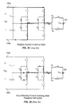
- Figs. 3A-D illustrate current flow during four switching states of the inverter 125:
- switches S 6 and S 7 are controlled by a PWM signal to turn “on” and turn “off” synchronously at a high frequency (e.g., 50 kHz), while switches S 2 and S 3 remain consistently in an "on” state.
- switches S 6 and S 7 are "on," as well as switches S 2 and S 3 .
- the current path in Fig. 3C is as follows: node 130a ⁇ S 7 ⁇ S 3 ⁇ L 2 ⁇ grid 120 ⁇ L 1 ⁇ S 2 ⁇ S 6 ⁇ node 130b.
- the current (called free-wheel current) flows through S 2 ⁇ D 10 ⁇ D 11 ⁇ S 3 ⁇ L 2 ⁇ grid 120 ⁇ L 1 .
- embodiments of the invention include an inverter having a free-wheel current state with current flowing through two switches and one diode; one less diode than the inverter 125. Accordingly, embodiments of the invention include an inverter with an improved efficiency.
- Fig. 4 depicts an inverter 150 with improved efficiency according to embodiments of the invention.
- the inverter 150 inverts DC power received via nodes 130a and 130b and outputs AC power to the grid 120 via nodes 140a and 140b.
- the inverter 150 is transformerless and has an NPC topology to prevent leakage current.
- the inverter 150 may serve as inverter 115 in system 100 of Fig.
- the inverter 150 includes eight MOSFET switching elements (S 1 -S 8 ), eight diodes (D 1 -D 8 ) associated with the switching elements, four additional diodes (D 9 -D 12 ) to control common mode voltage, two capacitors (C 1 , C 2 ), and two filter inductors (L 1 , L 2 ). Additionally, as will be explained in greater detail below, the inverter 150 includes two diodes D 13 and D 14 to provide high-efficiency, free-wheel current paths.
- the switching elements S 1 , S 2 , S 5 , and S 6 are part of a first three-level neutral point clamped bridge, and the switching elements S 3 , S 4 , S 7 , and S 8 are part of a second three-level neutral point clamped bridge.
- the inverter 150 is monitored and controlled by a controller 155.
- the controller 155 receives signals from sensors to monitor the inverter 150 including, for instance, current and voltage sensors for measuring V DC , i DC , V AC , and i AC .
- the inverter controller 155 may monitor the voltage and current at nodes 130a and 130b, and the grid 120. Based on the monitoring, the controller 155 selectively controls the switching elements S 1 -S 8 to invert the DC power received via nodes 130a and 130b and to provide AC power to the grid 120 synchronously via nodes 140a and 140b.
- the control signals to the switching elements S 1 -S 8 may include pulse-width modulated (PWM) signals.
- the controller 155 is one of a microcontroller, a microprocessor with appropriate memory and I/O devices, a field programmable gate array (FPGA), an application specific integrated circuit (ASIC), a digital signal processor (DSP), or the like.
- Figs. 5A-D illustrate current flow during four switching states of the inverter 150: a positive current switching state for a positive half-cycle ( Fig. 5A ); a free-wheel current state for the positive half-cycle ( Fig. 5B ); a negative current switching state for a negative half-cycle ( Fig. 5C ); and a free-wheel current state for the negative half-cycle ( Fig. 5D ).
- switches S 5 and S 8 are controlled by a PWM signal to turn "on” and turn “off” synchronously at a high frequency (e.g., 50 kHz), while switches S 1 and S 4 remain consistently “on.”
- a high frequency e.g. 50 kHz
- switches S 5 and S 8 are "on," along with switches S 1 and S 4 .
- the current path in Fig. 5A (positive current path 160) is as follows: node 130a ⁇ S 5 ⁇ S 1 ⁇ L 1 ⁇ grid 120 ⁇ L 2 ⁇ S 4 ⁇ S 8 ⁇ node 130b.
- the free-wheel current flows through a free-wheel current path 165, which includes S 1 ⁇ L 1 ⁇ grid 120 ⁇ L 2 ⁇ S 4 ⁇ D 14 .
- a free-wheel current path 165 which includes S 1 ⁇ L 1 ⁇ grid 120 ⁇ L 2 ⁇ S 4 ⁇ D 14 .
- current flows through only one diode (D 14 ), rather than two diodes (D 9 and D 12 ) as shown in Fig. 3B for the inverter 125. Accordingly, the efficiency of the inverter 150 is improved during the free-wheel current stage for the positive half-cycle as compared with the inverter 125.
- the common mode voltage of the inverter 150 is shown to be constant. Accordingly, the leakage current of the inverter 125 is controlled.
- the diodes D 9 -D 12 allow current to flow and clamp stray voltage to the middle point of the input voltage (i.e., the node connecting C 1 and C 2 ) to reduce common-mode voltage influence.
- Fig. 5C illustrates the negative current switching state
- Fig. 5D illustrates the negative free-wheel current state for the inverter 150.
- switches S 6 and S 7 are controlled by a PWM signal of the controller 155 to turn on and turn off synchronously at a high frequency (e.g., 50 kHz), while switches S 2 and S 3 remain consistently in an "on" state.
- a high frequency e.g. 50 kHz
- switches S 2 and S 3 remain consistently in an "on” state.
- switches S 6 and S 7 are "on,” as shown in Fig. 5C , the current flows from the input node 130a to the grid 120 and out through node 130b.
- the current path in Fig. 5C (negative current path 170) is as follows: node 130a ⁇ S 7 ⁇ S 3 ⁇ L 1 ⁇ grid 120 ⁇ L 2 ⁇ S 2 ⁇ S 6 ⁇ node 130b.
- the free-wheel current flows through a free-wheel current path 175, which includes S 2 ⁇ D 13 ⁇ S 3 ⁇ L 2 ⁇ grid 120 ⁇ L 1 .
- a free-wheel current path 175 which includes S 2 ⁇ D 13 ⁇ S 3 ⁇ L 2 ⁇ grid 120 ⁇ L 1 .
- current flows through only one diode (D 13 ), rather than two diodes (D 10 and D 11 ) as shown in Fig. 3D for the inverter 125. Accordingly, the efficiency of the inverter 150 is improved during the free-wheel current stage for the negative half-cycle as compared with the inverter 125.
- the diodes D 9 -D 12 allow current to flow and clamp stray voltage to the middle point of the input voltage to reduce common mode voltage influence.
- the diodes D 9 -D 12 are used to control the clamped point voltage. However, free-wheel current passes through the diodes D 13 and D 14 , not through the diodes D 9 -D 12 . Current flow resulting from controlling the clamped-point voltage is lower than free-wheel current.
- the diodes D 9 -D 12 in the inverter 125 must be able to handle the free-wheel current and, therefore, must have a higher power rating than diodes D 9 -D 12 of the inverter 150. Accordingly, the diodes D 9 -D 12 of the inverter 150 may have lower-power ratings than the diodes D 9 -D 12 of the inverter 125.
- the inverter 150 with exemplary components and switching control was shown to have an improved efficiency of approximately 0.1% relative to the inverter 125 during normal operation with similar components and switching control. For distributed power applications, such an improvement is substantial.
- "normal operation” included input voltage levels between approximately 260 V and 600 V, approximate component temperature of 75° C, and a power grid being a 240 V/60 Hz split-grid system.
- the tested inverters were 3 kW and 4 kW and had a power switching frequency of 50 kHz. Table 1 (below) shows the results of the experiment.
- Fig. 6 depicts a method 200 of inverting DC power to AC power using the inverter 150.
- step 205 the inverter 150 receives DC power via nodes 130a and 130b from the DC/DC converter 110. Although receiving DC power in step 205 is shown as a singular event, step 205 continues throughout the execution of the method 200. In other words, the inverter 150 receives DC power via nodes 130a and 130b throughout steps 210-235.
- step 210 the controller 155 controls the switching elements S 1 -S 8 to create the positive current path 160 shown in Fig. 5A .
- switches S 1 , S 4 , S 5 , and S 8 are turned “on,” and switches S 2 , S 3 , S 6 , and S 7 are turned “off.”
- the controller 155 controls the switching elements S 1 -S 8 to create the free-wheeling current path 165 for the positive half-cycle, as shown in Fig. 5B .
- switches S 5 and S 8 are turned “off” such that switches S 1 and S 4 remain “on,” and switches S 2 , S 3 , S 5 , S 6 , S 7 and S 8 are "off.”
- the AC power output by the inverter 150 is synchronized with the grid 120.
- the sinusoidal AC power output by the inverter 150 has a frequency (f). Accordingly, each full cycle of the sinusoidal output is 1/f seconds, and each half-cycle is 1/2 seconds.
- the inverter 150 switches between the positive current path 160 and the free-wheeling current path 165 as necessary to output AC power appropriately to the grid 120.
- the controller 155 determines whether to remain in the positive half-cycle. The controller 155 determines to enter the negative half-cycle based on sensor input data received. Assuming the grid 120 and inverter 150 outputs 60 Hz AC power, the inverter 150 will switch between the positive half-cycle and negative half-cycle approximately every 1/120 of a second.
- step 225 the controller 155 controls the switching elements S 1 -S 8 to create the negative current path 170 shown in Fig. 5C .
- switches S 1 , S 4 , S 5 , and S 8 are turned “off,” and switches S 2 , S 3 , S 6 , and S 7 are turned “on.”
- the controller 155 controls the switching elements S 1 -S 8 to create the free-wheeling current path 175 for the negative half-cycle, as shown in Fig. 5D .
- switches S 6 and S 7 are turned “off” such that switches S 2 and S 3 remain “on,” and switches S 1 , S 4 , S 5 , S 6 , S 7 and S 8 are "off.”
- step 235 the controller 155 determines whether to return to the positive half-cycle (step 210) or to return to step 225.
- the inverter 150 is described as being used with a PV panel 105, other DC sources may be used.
- a DC battery e.g., a fossil-fuel powered DC generator, a wind-powered DC generator, bio-fuel powered DC generator, a DC rectified AC power source (e.g., wind-powered AC generator), or another device that outputs DC power may be used.
- the PV panel 105 or DC sources are integrated with one more of the DC/DC converter 110 and inverter 125.
- embodiments of the invention provide, among other things, a highly efficient transformerless inverter and a method of controlling the same.
- Various features and advantages of the invention are set forth in the following claims.
Landscapes
- Engineering & Computer Science (AREA)
- Power Engineering (AREA)
- Inverter Devices (AREA)
- Supply And Distribution Of Alternating Current (AREA)
- Control Of Electrical Variables (AREA)
Abstract
Description
- The present invention relates to electrical inverters. More particularly, the invention relates to a three-level, single-phase inverter. The inverter has applicability to grid-connected systems.
- Inverters are devices that convert direct current (DC) to alternating current (AC). One type of inverter may be constructed by connecting a DC source to a transformer through the center tap of the primary winding of the transformer. A switch connected to the DC source is rapidly switched between two nodes (each of which is connected to opposite sides of the primary winding) to allow current to flow back to the DC source through two alternate paths: through one end of the primary winding and then the other. The alternation of the direction of current in the primary winding of the transformer produces alternating current (or AC) in the secondary winding. Inverters of this design or other designs may receive DC power from, for instance, solar panels, generators, wind turbines, batteries, and other sources, convert the DC power to AC power, and export the AC power to local loads or a power grid.
- Such inverters, and other inverters including a transformer, provide galvanic isolation between the DC input and the AC output. However, these transformers have severe drawbacks, like high weight, high cost, low efficiency, and a non-unity power factor, especially under low load conditions. High frequency inverters with transformers may reduce weight and have unity power factor, but do not improve the efficiency of the power inversion.
- Transformerless inverters convert DC power to AC power without the use of a transformer along the DC-to-AC conversion path. Rather than a transformer, transformerless inverters include power switching elements, such as MOSFET and/or IGBT transistors, that are particularly arranged and controlled to convert received DC power to AC power and to reduce the influence between DC input and AC output. Regardless of the design, energy is lost in an inverter during the conversion of DC power to AC power. The less energy lost in the conversion, the more efficient the inverter. Transformerless inverters, although often more complex, are generally more efficient than inverters with transformers.
- While generally more efficient than transformer-based inverters, the inventor(s) has (have) learned that the efficiency of transformerless inverters is not as high as desired for certain applications. Embodiments of the invention include a transformerless inverter with improved efficiency. In a particular instance, the invention provides a grid-connectable inverter that has a first DC input node and a second DC input node; a first AC output node and a second AC output node. The inverter also includes a first switch, a second switch, a third switch, a fourth switch, a first diode, and a second diode. The inverter further includes four paths: a positive current path for a positive half-cycle, a first free-wheel current path for the positive half-cycle, a negative current path for a negative half-cycle and a second free-wheel current path for the negative half-cycle. The first free-wheel current path includes the first AC output node, the first switch, the first diode, the fourth switch, and the second AC output node. In the first free-wheel current path, no additional diode is connected in series with the first diode between the first switch and fourth switch. The second free-wheel current path includes the second AC output node, the second switch, the second diode, the third switch, and the first AC output node. In the second free-wheel current path, no additional diode is connected in series with the second diode between the second switch and third switch.
- Embodiments of the invention also provide a method of inverting DC power to AC power with a grid-connectable inverter. The inverter includes first and second DC input nodes, first and second AC output nodes, four switches (a first, second, third, and fourth), a first diode, and a second diode. The method includes receiving DC input at the first and second DC input node. At least the first, second, third, and fourth switches are controlled to create a positive current path for a positive half-cycle. Also during the positive half-cycle, the first switch and the fourth switch are closed to create a first free-wheel current path. The first free-wheel current path includes the first AC output node, the first switch, the first diode, the fourth switch, and the second AC output node. In the first free-wheel current path, no additional diode is connected in series with the first diode between the first and fourth switch. The method further includes controlling at least the first, second, third, and fourth switches to create a negative current path for a negative half-cycle. During the negative half-cycle, the second switch and the third switch are closed to create a second free-wheel current path for the negative half-cycle. The second free-wheel current path includes the second AC output node, the second switch, the second diode, the third switch, and the first AC output node. In the second free-wheel current path, no additional diode is connected in series with the second diode between the second and third switch.
- Other aspects of the invention will become apparent by consideration of the detailed description and accompanying drawings.
-
Fig. 1 depicts a power conversion system. -
Fig. 2 depicts a prior-art, three-level transformerless inverter. -
Figs. 3A-D depict the four switching states, respectively, of the prior-art, three-level transformerless inverter. -
Fig. 4 depicts a three-level transformerless inverter according to embodiments of the invention. -
Figs. 5A-D depict the four switching states, respectively, of a three-level transformerless inverter according to embodiments of the invention. -
Fig. 6 depicts a method of inverting DC power to AC power according to embodiments of the invention. - Before any embodiments of the invention are explained in detail, it is to be understood that the invention is not limited in its application to the details of construction and the arrangement of components set forth in the following description or illustrated in the following drawings. The invention is capable of other embodiments and of being practiced or of being carried out in various ways.
-
Fig. 1 illustrates apower conversion system 100. Thepower conversion system 100 includes a photovoltaic (PV)panel 105, a DC/DC converter 110, an inverter 115, and anAC grid 120. ThePV panel 105 receives solar radiation and converts the radiation to DC power. The PV panel outputs the DC power to the DC/DC converter 110. The DC/DC converter 110 bucks or boosts the DC power to a level appropriate for the inverter 115. For instance, the DC/DC converter 110 provides a DC output with predetermined characteristics such as a particular voltage within a defined tolerance. The DC/DC converter 110 can be considered as providing "conditioned power" and it may be a transformerless converter or it may contain a transformer. The inverter 115 receives the conditioned DC power from the DC/DC converter 110 and inverts the DC power to AC power. The inverter 115 then outputs the AC power to theAC grid 120. - A power grid (sometimes simply referred to as a "grid" herein), such as
grid 120, is a system of transmission lines and other devices by which electrical power generated by an electric utility company is transmitted to customers. Stated another way, thegrid 120 is an electrical network that interconnects one or more AC power suppliers with one or more AC power consumers. Taking, for example, an individual home or facility including the inverter 115, thegrid 120 may connect the inverter 115 with an external electrical utility grid, with local power-consuming devices (e.g., loads connected to outlets in or nearby the home), or both. In normal operation, thegrid 120 provides AC power with a sinusoidal voltage waveform with an approximately constant magnitude and frequency (e.g., 120 V at 60 Hz when delivered to a local sub-section of the grid powering homes). In other parts or at other delivery points, the power provided bygrid 120 may have various magnitudes (e.g., 208 V, 240 V, 277 V, to many kV) and frequencies (e.g., 50 Hz or 60 Hz) depending on the implementation or local standards. The inverter 115 has applicability to systems that are "grid connected" or tied to thegrid 120. Although, it is possible to connect the inverter 115 (with additional equipment not shown) to a local electrical system or local loads ("off grid") instead of thegrid 120. -
Fig. 2 illustrates a prior-art, three-level transformerless inverter 125 having a neutral point clamped (NPC) topology. Theinverter 125 is an exemplary inverter 115 ofFig. 1 . Although the NPC topology ofFig. 2 has more switching elements than a traditional H-bridge circuit, the NPC topology has a reduced voltage rating value and reduces the influence of common mode voltage. Common mode voltage in inverter systems can produce leakage currents, which are potentially harmful. For instance, if leakage currents are present, voltage can build on stray capacitances of a PV panel. If an individual contacts the PV panel and is connected to ground, the leakage current can discharge through the individual. - The
inverter 125 includes eight switching elements (S1-S8), eight diodes (D1-D8) associated with the switching elements, four additional diodes (D9-D12), two capacitors (C1, C2), and two filter inductors (L1, L2). The switching elements S1-S8 are MOSFET transistors, and the diodes D1-D8 are reverse body diodes for the switching elements S1-S8. Theinverter 125 receives a VDC input acrossnodes inverter 125 may be coupled to a PV panel and DC/DC converter as shown inFig. 1 . The VDC input is inverted and output to theAC grid 120 vianodes - Throughout this description, the terms "on" and "off" are used in describing components of circuit diagrams. When used with a switching element, the term "on" indicates (in the case of a MOSFET) that a voltage is applied to the control terminal of the switching element (e.g., the gate) such that current can flow through the other terminals (e.g., the source and drain). The term "off" indicates that no or a low voltage is applied to the gate of the switching element and there is no (or negligible) current flow between the drain and source. In figures of the present application, transistors that are "on" are shown as conducting wires, while transistors that are "off" are shown as an open switch. The term "on" when used with a diode indicates that the diode is conducting electricity in a forward-bias direction. The term "off" when used with a diode indicates that the diode is not conducting electricity (in any direction). While the transistors and diodes have more complicated electrical characteristics and responses, these depictions provide a simplified explanation of the inverter circuits described herein.
-
Figs. 3A-D illustrate current flow during four switching states of the inverter 125: - a positive current switching state for a positive half-cycle (
Fig. 3A ); - a free-wheel current state for the positive half-cycle (
Fig. 3B ); - a negative current switching state for a negative half-cycle (
Fig. 3C ); and - a free-wheel current state for the negative half-cycle (
Fig. 3D ). - In the negative switching states of
Figs. 3C-D , switches S6 and S7 are controlled by a PWM signal to turn "on" and turn "off" synchronously at a high frequency (e.g., 50 kHz), while switches S2 and S3 remain consistently in an "on" state. InFig. 3C , switches S6 and S7 are "on," as well as switches S2 and S3. The current path inFig. 3C is as follows:node 130a → S7 → S3 → L2 →grid 120 → L1 → S2 → S6 →node 130b. With switches S6 and S7 off as shown inFig. 3D , the current (called free-wheel current) flows through S2 → D10 → D11 → S3 → L2 →grid 120 → L1. - In the four states of the
inverter 125, the common mode voltage is held constant. More specifically, in positive current switching state (Fig. 3A ), the common mode voltage is:
- During free-wheel periods, the diodes D9-D12 allow current to flow and clamp voltage to the middle point of input voltage to reduce common mode voltage influence. In the positive free-wheel current switching state (
Fig. 3B ), the common mode voltage is:
- A similar analysis applies to the negative switching states of
Figs. 3C-D . Accordingly, the common mode voltage of theinverter 125 is held at half of the input voltage (VDC) through the four switching states, and the leakage current of theinverter 125 is controlled. - In free-wheel current states of a three-level transformerless inverter, such as shown in
Figs. 3B and3D forinverter 125, the inverter efficiency is decreased with each additional circuit component (i.e., switch or diode) within the current path. In the free-wheel current state shown inFig. 3B , the current flows through two diodes (D12, D9) and two switches (S1, S4). Similarly, in the free-wheel current state shown inFig. 3D , the current flows through two diodes (D10, D11) and two switches (S2, S3). As explained in greater detail below, embodiments of the invention include an inverter having a free-wheel current state with current flowing through two switches and one diode; one less diode than theinverter 125. Accordingly, embodiments of the invention include an inverter with an improved efficiency. -
Fig. 4 depicts aninverter 150 with improved efficiency according to embodiments of the invention. Theinverter 150 inverts DC power received vianodes grid 120 vianodes inverter 125, theinverter 150 is transformerless and has an NPC topology to prevent leakage current. Also like theinverter 125, theinverter 150 may serve as inverter 115 insystem 100 ofFig. 1 , and theinverter 150 includes eight MOSFET switching elements (S1-S8), eight diodes (D1-D8) associated with the switching elements, four additional diodes (D9-D12) to control common mode voltage, two capacitors (C1, C2), and two filter inductors (L1, L2). Additionally, as will be explained in greater detail below, theinverter 150 includes two diodes D13 and D14 to provide high-efficiency, free-wheel current paths. The switching elements S1, S2, S5, and S6 are part of a first three-level neutral point clamped bridge, and the switching elements S3, S4, S7, and S8 are part of a second three-level neutral point clamped bridge. - The
inverter 150 is monitored and controlled by acontroller 155. Thecontroller 155 receives signals from sensors to monitor theinverter 150 including, for instance, current and voltage sensors for measuring VDC, iDC, VAC, and iAC. For instance, theinverter controller 155 may monitor the voltage and current atnodes grid 120. Based on the monitoring, thecontroller 155 selectively controls the switching elements S1-S8 to invert the DC power received vianodes grid 120 synchronously vianodes controller 155 is one of a microcontroller, a microprocessor with appropriate memory and I/O devices, a field programmable gate array (FPGA), an application specific integrated circuit (ASIC), a digital signal processor (DSP), or the like. -
Figs. 5A-D illustrate current flow during four switching states of the inverter 150: a positive current switching state for a positive half-cycle (Fig. 5A ); a free-wheel current state for the positive half-cycle (Fig. 5B ); a negative current switching state for a negative half-cycle (Fig. 5C ); and a free-wheel current state for the negative half-cycle (Fig. 5D ). In the positive switching states ofFigs. 5A-B , switches S5 and S8 are controlled by a PWM signal to turn "on" and turn "off" synchronously at a high frequency (e.g., 50 kHz), while switches S1 and S4 remain consistently "on." InFig. 5A , switches S5 and S8 are "on," along with switches S1 and S4. The current path inFig. 5A (positive current path 160) is as follows:node 130a → S5 → S1 → L1 →grid 120 → L2 → S4 → S8 →node 130b. - When the switches S5 and S8 are off, as shown in
Fig. 5B , the free-wheel current flows through a free-wheelcurrent path 165, which includes S1 → L1 →grid 120 → L2 → S4 → D14. During the free-wheel current state for the positive half-cycle of theinverter 150, current flows through only one diode (D14), rather than two diodes (D9 and D12) as shown inFig. 3B for theinverter 125. Accordingly, the efficiency of theinverter 150 is improved during the free-wheel current stage for the positive half-cycle as compared with theinverter 125. - As with the
inverter 125, when switches S5 and S8 are "on," the common mode voltage is:
- Additionally, with switches S5 and S8 off, the common mode voltage is:

- Based on the above circuit analysis, the common mode voltage of the
inverter 150 is shown to be constant. Accordingly, the leakage current of theinverter 125 is controlled. During free-wheel periods, the diodes D9-D12 allow current to flow and clamp stray voltage to the middle point of the input voltage (i.e., the node connecting C1 and C2) to reduce common-mode voltage influence. -
Fig. 5C illustrates the negative current switching state andFig. 5D illustrates the negative free-wheel current state for theinverter 150. In the negative switching states ofFigs.3C-D , switches S6 and S7 are controlled by a PWM signal of thecontroller 155 to turn on and turn off synchronously at a high frequency (e.g., 50 kHz), while switches S2 and S3 remain consistently in an "on" state. When switches S6 and S7 are "on," as shown inFig. 5C , the current flows from theinput node 130a to thegrid 120 and out throughnode 130b. The current path inFig. 5C (negative current path 170) is as follows:node 130a → S7 → S3 → L1 →grid 120 → L2 → S2 → S6 →node 130b. - With switches S6 and S7 off as shown in
Fig. 5D , the free-wheel current flows through a free-wheelcurrent path 175, which includes S2 → D13 → S3 → L2 →grid 120 → L1. During the free-wheel current state for the negative half-cycle of theinverter 150, current flows through only one diode (D13), rather than two diodes (D10 and D11) as shown inFig. 3D for theinverter 125. Accordingly, the efficiency of theinverter 150 is improved during the free-wheel current stage for the negative half-cycle as compared with theinverter 125. - Similar to the common mode voltage of the
inverter 125, the common mode voltage of theinverter 150 is held constant in the four states of theinverter 150. More specifically, in positive current switching state (Fig. 5A ), the common mode voltage is:
- During free-wheel periods, the diodes D9-D12 allow current to flow and clamp stray voltage to the middle point of the input voltage to reduce common mode voltage influence. In the positive free-wheel current switching state (
Fig. 5B ), the common mode voltage is:
- A similar analysis applies to the negative switching states of
Figs. 5C-D . Accordingly, the common mode voltage of theinverter 150 is held at half of the input voltage (VDC) through the four switching states, and the leakage current of theinverter 150 is controlled. - In the
inverter 150, the diodes D9-D12 are used to control the clamped point voltage. However, free-wheel current passes through the diodes D13 and D14, not through the diodes D9-D12. Current flow resulting from controlling the clamped-point voltage is lower than free-wheel current. The diodes D9-D12 in theinverter 125 must be able to handle the free-wheel current and, therefore, must have a higher power rating than diodes D9-D12 of theinverter 150. Accordingly, the diodes D9-D12 of theinverter 150 may have lower-power ratings than the diodes D9-D12 of theinverter 125. - Through experimentation, the
inverter 150 with exemplary components and switching control was shown to have an improved efficiency of approximately 0.1% relative to theinverter 125 during normal operation with similar components and switching control. For distributed power applications, such an improvement is substantial. In this experiment, "normal operation" included input voltage levels between approximately 260 V and 600 V, approximate component temperature of 75° C, and a power grid being a 240 V/60 Hz split-grid system. The tested inverters were 3 kW and 4 kW and had a power switching frequency of 50 kHz. Table 1 (below) shows the results of the experiment.Table 1 Efficiency calculation results Input Voltage 3kW 4kW Inverter 125 Inverter 150Inverter 125Inverter 150Weighted η 260 V 96.46% 96.55% 96.41% 96.51% 365 V 97.24% 97.33% 97.25% 97.35% 480 V 97.10% 97.27% 97.12% 97.30% CEC η 96.93% 97.05% 96.94% 97.05% - As shown in Table 2, efficiency improvements were present for low input voltages (e.g., less than 200 V), but were less substantial.
Table 2 Efficiency calculation results at low input voltage Input Voltage 3kW 4kW Inverter 125 Inverter 150Inverter 125Inverter 150Weighted η 150 V 95.51% 95.60% 95.26% 95.36% 200 V 96.11% 96.20% 96.00% 96.10% - Of course, the above data is from an exemplary experiment with particularly assumed operational parameters (e.g., circuit components, switching control techniques, environment, etc.). The particular efficiency improvements vary depending on the operational parameters of the
inverter 150. -
Fig. 6 depicts amethod 200 of inverting DC power to AC power using theinverter 150. Instep 205, theinverter 150 receives DC power vianodes DC converter 110. Although receiving DC power instep 205 is shown as a singular event,step 205 continues throughout the execution of themethod 200. In other words, theinverter 150 receives DC power vianodes - In
step 210, thecontroller 155 controls the switching elements S1-S8 to create the positivecurrent path 160 shown inFig. 5A . To create the positivecurrent path 160, switches S1, S4, S5, and S8 are turned "on," and switches S2, S3, S6, and S7 are turned "off." After a certain time period, instep 215, thecontroller 155 controls the switching elements S1-S8 to create the free-wheelingcurrent path 165 for the positive half-cycle, as shown inFig. 5B . To create the free-wheelingcurrent path 165, switches S5 and S8 are turned "off" such that switches S1 and S4 remain "on," and switches S2, S3, S5, S6, S7 and S8 are "off." - The AC power output by the
inverter 150 is synchronized with thegrid 120. The sinusoidal AC power output by theinverter 150 has a frequency (f). Accordingly, each full cycle of the sinusoidal output is 1/f seconds, and each half-cycle is 1/2 seconds. During the positive half-cycle, theinverter 150 switches between the positivecurrent path 160 and the free-wheelingcurrent path 165 as necessary to output AC power appropriately to thegrid 120. Instep 220, thecontroller 155 determines whether to remain in the positive half-cycle. Thecontroller 155 determines to enter the negative half-cycle based on sensor input data received. Assuming thegrid 120 andinverter 150 outputs 60 Hz AC power, theinverter 150 will switch between the positive half-cycle and negative half-cycle approximately every 1/120 of a second. - In
step 225, thecontroller 155 controls the switching elements S1-S8 to create the negativecurrent path 170 shown inFig. 5C . To create the negativecurrent path 170, switches S1, S4, S5, and S8 are turned "off," and switches S2, S3, S6, and S7 are turned "on." After a certain time period, instep 230, thecontroller 155 controls the switching elements S1-S8 to create the free-wheelingcurrent path 175 for the negative half-cycle, as shown inFig. 5D . To create the free-wheelingcurrent path 175, switches S6 and S7 are turned "off" such that switches S2 and S3 remain "on," and switches S1, S4, S5, S6, S7 and S8 are "off." - During the negative half-cycle, the
inverter 150 switches between the negativecurrent path 170 and the free-wheelingcurrent path 175 as necessary to output AC power appropriately to thegrid 120. Instep 235, thecontroller 155 determines whether to return to the positive half-cycle (step 210) or to return tostep 225. - Although the
inverter 150 is described as being used with aPV panel 105, other DC sources may be used. For instance, in place of thePV panel 105, one or more of a DC battery, a fossil-fuel powered DC generator, a wind-powered DC generator, bio-fuel powered DC generator, a DC rectified AC power source (e.g., wind-powered AC generator), or another device that outputs DC power may be used. In some embodiments, thePV panel 105 or DC sources are integrated with one more of the DC/DC converter 110 andinverter 125. - Thus, embodiments of the invention provide, among other things, a highly efficient transformerless inverter and a method of controlling the same. Various features and advantages of the invention are set forth in the following claims.
Claims (20)
- A grid-connectable inverter comprising:a first DC input node and a second DC input node;a first AC output node and a second AC output node;a first switch, a second switch, a third switch, and a fourth switch;a first diode and a second diode;a positive current path for a positive half-cycle;a first free-wheel current path for the positive half-cycle, wherein the first free-wheel current path includes the first AC output node, the first switch, the first diode, the fourth switch, and the second AC output node, and wherein no additional diode is connected in series with the first diode between the first and fourth switch;a negative current path for a negative half-cycle; anda second free-wheel current path for the negative half-cycle, wherein the second free-wheel current path includes the second AC output node, the second switch, the second diode, the third switch, and the first AC output node, and wherein no additional diode is connected in series with the second diode between the second and third switch.
- The grid-connectable inverter of claim 1, further comprising a fifth switch and an eighth switch, wherein the positive current path includes the first DC input node, the fifth switch, the first switch, the second AC output node, the first AC output node, the fourth switch, the eighth switch, and the second DC input node.
- The grid-connectable inverter of claim 1, further comprising a sixth switch and a seventh switch, wherein the negative current path includes the first DC input node, the seventh switch, the third switch, the first AC output node, the second AC output node, the second switch, the third switch, and the second DC input node.
- The grid-connectable inverter of claim 1, wherein the first AC output node has a first voltage and the second AC output node has a second voltage, and wherein half of the sum of the first voltage and the second voltage remains substantially constant while the inverter is in the positive half-cycle and the negative cycle.
- The grid-connectable inverter of claim 1, wherein the first AC output node and the second AC output node are coupled to an AC grid.
- The grid-connectable inverter of claim 1, wherein the first DC input node and the second DC input node are coupled to outputs of a DC to DC converter.
- The grid-connectable inverter of claim 6, wherein inputs of the DC to DC converter are coupled to a photovoltaic array.
- The grid-connectable inverter of claim 1, further comprising a controller for selectively controlling the first switch, the second switch, the third switch, and the fourth switch.
- The grid-connectable inverter of claim 8, wherein the controller selectively controls the first switch, the second switch, the third switch, and the fourth switch based on signals from sensors monitoring at least one of current at the first DC input node, voltage at the first DC input node, current of an AC grid to which the inverter is coupled, and voltage of the AC grid.
- The grid-connectable inverter of claim 1, wherein the first switch and the second switch form a portion of a first three-level neutral point clamped bridge and the third switch and the fourth switch form a portion of a second three-level neutral point clamped bridge.
- A method of inverting DC power to AC power with a grid-connectable inverter including first and second DC input nodes, first and second AC output nodes, first, second, third, and fourth switches, and first and second diodes, the method comprising:receiving DC input at the first and second DC input node;controlling the first, second, third, and fourth switches to create a positive current path for a positive half-cycle;closing the first switch and the fourth switch to create a first free-wheel current path for the positive half-cycle, wherein the first free-wheel current path includes the first AC output node, the first switch, the first diode, the fourth switch, and the second AC output node, and wherein no additional diode is connected in series with the first diode between the first and fourth switch;controlling the first, second, third, and fourth switches to create a negative current path for a negative half-cycle; andclosing the second switch and the third switch to create a second free-wheel current path for the negative half-cycle, wherein the second free-wheel current path includes the second AC output node, the second switch, the second diode, the third switch, and the first AC output node, and wherein no additional diode is connected in series with the second diode between the second and third switch.
- The method of claim 11, further comprising controlling a fifth switch and an eighth switch to create the positive current path, wherein the positive current path includes the first DC input node, the fifth switch, the first switch, the second AC output node, the first AC output node, the fourth switch, the eighth switch, and the second DC input node.
- The method of claim 11, further comprising controlling a sixth switch and a seventh switch to create the negative current path, wherein the negative current path includes the first DC input node, the seventh switch, the third switch, the first AC output node, the second AC output node, the second switch, the third switch, and the second DC input node.
- The method of claim 11, wherein the first AC output node has a first voltage and the second AC output node has a second voltage, and wherein half of the sum of the first voltage and the second voltage remains substantially constant while the inverter is in the positive half-cycle and the negative cycle.
- The method of claim 11, further comprising coupling the first AC output node and the second AC output node to an AC grid.
- The method of claim 11, further comprising coupling the first DC input node and the second DC input node to outputs of a DC to DC converter.
- The method of claim 16, further comprising coupling inputs of the DC to DC converter to a photovoltaic array.
- The method of claim 11, wherein the DC input is inverted by selectively directing a flow of current through the positive current path, the first free-wheel current path, the negative current path, and the second free-wheel current path.
- The method of claim 11, wherein the first, second, third, and fourth switches are controlled by a controller based on signals from sensors monitoring at least one of current at the first DC input node, voltage at the first DC input node, current of an AC grid to which the inverter is coupled, and voltage of the AC grid.
- The method of claim 11, wherein the first and second switches form a portion of a first three-level neutral point clamped bridge and the third and fourth switches form a portion of a second three-level neutral point clamped bridge.
Applications Claiming Priority (1)
| Application Number | Priority Date | Filing Date | Title |
|---|---|---|---|
| US13/331,539 US8867248B2 (en) | 2011-12-20 | 2011-12-20 | High-efficiency, three-level, single-phase inverter |
Publications (2)
| Publication Number | Publication Date |
|---|---|
| EP2608386A2 true EP2608386A2 (en) | 2013-06-26 |
| EP2608386A3 EP2608386A3 (en) | 2017-10-11 |
Family
ID=47552725
Family Applications (1)
| Application Number | Title | Priority Date | Filing Date |
|---|---|---|---|
| EP12007537.9A Withdrawn EP2608386A3 (en) | 2011-12-20 | 2012-11-06 | High-Efficiency, Three-Level, Single-Phase Inverter |
Country Status (3)
| Country | Link |
|---|---|
| US (1) | US8867248B2 (en) |
| EP (1) | EP2608386A3 (en) |
| CN (1) | CN103178733B (en) |
Cited By (3)
| Publication number | Priority date | Publication date | Assignee | Title |
|---|---|---|---|---|
| WO2015152745A1 (en) | 2014-04-05 | 2015-10-08 | Inov Inesc Inovação Instituto De Novas Tecnologias | Electronic energy conversion circuit, energy arrangement presenting said circuit and process of operation of said circuit |
| EP3214749A4 (en) * | 2014-10-29 | 2017-11-22 | Panasonic Intellectual Property Management Co., Ltd. | Power-converting device, and power conditioner using same |
| EP3563478A1 (en) * | 2016-12-30 | 2019-11-06 | SMA Solar Technology AG | A modulation method and apparatus based on three-phase neutral point clamped inverter |
Families Citing this family (25)
| Publication number | Priority date | Publication date | Assignee | Title |
|---|---|---|---|---|
| US8929114B2 (en) * | 2011-02-24 | 2015-01-06 | Virginia Tech Intellectual Properties, Inc. | Three-level active neutral point clamped zero voltage switching converter |
| DE102012205335A1 (en) * | 2012-04-02 | 2013-10-02 | Dr. Johannes Heidenhain Gmbh | inverter |
| JP5626293B2 (en) * | 2012-08-29 | 2014-11-19 | 株式会社村田製作所 | Inverter device |
| JP5598513B2 (en) * | 2012-08-29 | 2014-10-01 | 株式会社村田製作所 | Power system interconnection inverter device |
| WO2014061519A1 (en) * | 2012-10-17 | 2014-04-24 | 株式会社村田製作所 | Inverter device |
| US9941813B2 (en) | 2013-03-14 | 2018-04-10 | Solaredge Technologies Ltd. | High frequency multi-level inverter |
| US9654024B2 (en) * | 2013-05-30 | 2017-05-16 | Texas Instruments Incorporated | AC-DC converter having soft-switched totem-pole output |
| CN103346690B (en) | 2013-07-05 | 2016-03-30 | 华为技术有限公司 | A kind of multi-electrical level inverter and electric power system |
| NL2011648C2 (en) * | 2013-10-18 | 2015-04-23 | Prodrive B V | Switched power converter. |
| CN103700473B (en) * | 2013-12-12 | 2017-11-28 | 华为技术有限公司 | Coupling inductance and power inverter |
| DE102014203553A1 (en) * | 2014-02-27 | 2015-08-27 | Robert Bosch Gmbh | Electric drive system |
| US9318974B2 (en) | 2014-03-26 | 2016-04-19 | Solaredge Technologies Ltd. | Multi-level inverter with flying capacitor topology |
| DE102015104554A1 (en) * | 2014-05-16 | 2015-11-19 | Semikron Elektronik Gmbh & Co. Kg | circuitry |
| CN103973147B (en) * | 2014-05-31 | 2017-01-18 | 吉林大学 | Multi-level high-voltage grounded source electromagnetic transmitting circuit |
| US9555711B2 (en) * | 2014-06-03 | 2017-01-31 | Hamilton Sundstrand Corporation | Power converters |
| US20160241161A1 (en) * | 2015-02-12 | 2016-08-18 | Semikron Elektronik Gmbh & Co., Kg | Converting circuit |
| US20190157986A1 (en) * | 2015-09-16 | 2019-05-23 | sonnen GmbH | Inverter device, energy storage system and method of controlling an inverter device |
| CN105207607A (en) * | 2015-09-21 | 2015-12-30 | 北京科诺伟业科技股份有限公司 | Three-phase ABC alternating-current tandem type photovoltaic array |
| CN105634289A (en) * | 2016-01-27 | 2016-06-01 | 南京能瑞电力科技有限公司 | Output voltage control apparatus and method for full-bridge LLC resonant DC/DC converter |
| CN107294417B (en) * | 2017-07-17 | 2019-09-20 | 阳光电源股份有限公司 | An inverter and its control method, control device, and control system |
| US10097109B1 (en) * | 2017-07-19 | 2018-10-09 | Futurewei Technologies, Inc. | Three-level voltage bus apparatus and method |
| CN107994796B (en) * | 2017-12-26 | 2020-04-28 | 华为技术有限公司 | Control method and device for single-phase converter |
| US10965221B1 (en) * | 2020-09-01 | 2021-03-30 | King Abdulaziz University | Switched capacitor based boost inverter topology with a higher number of levels and higher voltage gain |
| US11159095B1 (en) * | 2020-11-12 | 2021-10-26 | King Abdulaziz University | 11-level boost active neutral point clamped inverter topology with higher voltage gain |
| US20230156887A1 (en) * | 2021-11-18 | 2023-05-18 | Guang Zhou Ting Shen Electric Co., Ltd. | High Voltage Controller |
Citations (1)
| Publication number | Priority date | Publication date | Assignee | Title |
|---|---|---|---|---|
| US20110096581A1 (en) * | 2008-06-25 | 2011-04-28 | Jalal Hallak | Inverter and method for operating the inverter |
Family Cites Families (23)
| Publication number | Priority date | Publication date | Assignee | Title |
|---|---|---|---|---|
| JP3243666B2 (en) | 1993-04-01 | 2002-01-07 | 株式会社日立メディコ | Resonant DC-DC converter |
| JP3263317B2 (en) | 1996-06-18 | 2002-03-04 | 株式会社東芝 | Switching module and power converter using the module |
| DE10221592A1 (en) | 2002-05-15 | 2003-12-04 | Fraunhofer Ges Forschung | Inverter and method for converting a DC electrical voltage into an AC current |
| US6838925B1 (en) | 2003-10-07 | 2005-01-04 | American Power Conversion Corporation | Three level inverter |
| JP4357279B2 (en) * | 2003-12-04 | 2009-11-04 | 株式会社東芝 | Converter circuit in electric vehicle control device |
| DE102004030912B3 (en) | 2004-06-25 | 2006-01-19 | Sma Technologie Ag | Method for converting a direct electrical voltage of a DC voltage source, in particular a photovoltaic DC voltage source into an AC voltage |
| JP4164050B2 (en) | 2004-07-29 | 2008-10-08 | 株式会社日立製作所 | Grid interconnection device |
| DE102005047373A1 (en) | 2005-09-28 | 2007-04-05 | Schekulin, Dirk, Dr. Ing. | Buck converter circuit and inverter circuit arrangement |
| US7378820B2 (en) | 2005-12-19 | 2008-05-27 | General Electric Company | Electrical power generation system and method for generating electrical power |
| DE102006010694B4 (en) | 2006-03-08 | 2010-01-07 | Refu Elektronik Gmbh | Inverter circuit for extended input voltage range |
| TWI307571B (en) * | 2006-03-31 | 2009-03-11 | Delta Electronics Inc | Current source inverter with energy clamp circuit and controlling method thereof having relatively better effectiveness |
| EP2051364A3 (en) | 2007-10-19 | 2016-08-10 | Diehl AKO Stiftung & Co. KG | Method for operating an inverter |
| DE502007002360D1 (en) | 2007-10-19 | 2010-01-28 | Sma Solar Technology Ag | Inverters, in particular for photovoltaic installations |
| DE102008050765A1 (en) | 2008-02-08 | 2009-08-20 | Fraunhofer-Gesellschaft zur Förderung der angewandten Forschung e.V. | Inverter arrangement for feeding photovoltaic energy into a public grid |
| JP5205094B2 (en) * | 2008-03-24 | 2013-06-05 | 東芝三菱電機産業システム株式会社 | Inverter control device |
| DE102008048841B8 (en) | 2008-09-25 | 2010-06-10 | Fraunhofer-Gesellschaft zur Förderung der angewandten Forschung e.V. | Isolating circuit for inverter |
| WO2010044164A1 (en) | 2008-10-16 | 2010-04-22 | 東芝三菱電機産業システム株式会社 | Power converter |
| TWI413356B (en) * | 2008-12-12 | 2013-10-21 | Delta Electronics Inc | Inverter circuit having relatively higher efficiency |
| CN101515763B (en) * | 2009-03-27 | 2010-11-10 | 南京航空航天大学 | Series-parallel output three-level half-bridge inverter and its half-period hysteresis control method |
| US8582331B2 (en) | 2009-07-20 | 2013-11-12 | Vincotech Holdings S.à.r.l. | Inverter topologies usable with reactive power |
| CN101783611B (en) * | 2010-01-15 | 2012-03-21 | 南京航空航天大学 | Split induction three-level photovoltaic grid-connected inverter and control method thereof |
| CN101980437B (en) * | 2010-10-22 | 2012-07-04 | 南京航空航天大学 | Five-level grid-connected inverter |
| CN102185514B (en) * | 2011-03-10 | 2013-07-10 | 浙江大学 | Single-phase three-level inverter |
-
2011
- 2011-12-20 US US13/331,539 patent/US8867248B2/en active Active
-
2012
- 2012-11-06 EP EP12007537.9A patent/EP2608386A3/en not_active Withdrawn
- 2012-11-16 CN CN201210466120.1A patent/CN103178733B/en not_active Expired - Fee Related
Patent Citations (1)
| Publication number | Priority date | Publication date | Assignee | Title |
|---|---|---|---|---|
| US20110096581A1 (en) * | 2008-06-25 | 2011-04-28 | Jalal Hallak | Inverter and method for operating the inverter |
Non-Patent Citations (1)
| Title |
|---|
| 00 REV 0: "50W, 500kHz, Full-Bridge, Phase-Shift, ZVS Isolated DC to DC Converter Using the HIP4081A", 1 April 1995 (1995-04-01), pages 1 - 18, XP055780774, Retrieved from the Internet <URL:https://www.renesas.com/eu/en/document/apn/an9506-50w-500khz-full-bridge-phase-shift-zvs-isolated-dc-dc-converter-using-hip4081a?language=en> [retrieved on 20210301] * |
Cited By (4)
| Publication number | Priority date | Publication date | Assignee | Title |
|---|---|---|---|---|
| WO2015152745A1 (en) | 2014-04-05 | 2015-10-08 | Inov Inesc Inovação Instituto De Novas Tecnologias | Electronic energy conversion circuit, energy arrangement presenting said circuit and process of operation of said circuit |
| EP3214749A4 (en) * | 2014-10-29 | 2017-11-22 | Panasonic Intellectual Property Management Co., Ltd. | Power-converting device, and power conditioner using same |
| US9893648B2 (en) | 2014-10-29 | 2018-02-13 | Panasonic Intellectual Property Management Co., Ltd. | Power converting device, and power conditioner using same |
| EP3563478A1 (en) * | 2016-12-30 | 2019-11-06 | SMA Solar Technology AG | A modulation method and apparatus based on three-phase neutral point clamped inverter |
Also Published As
| Publication number | Publication date |
|---|---|
| CN103178733A (en) | 2013-06-26 |
| EP2608386A3 (en) | 2017-10-11 |
| US8867248B2 (en) | 2014-10-21 |
| CN103178733B (en) | 2015-09-09 |
| US20130155747A1 (en) | 2013-06-20 |
Similar Documents
| Publication | Publication Date | Title |
|---|---|---|
| US8867248B2 (en) | High-efficiency, three-level, single-phase inverter | |
| US9800167B2 (en) | Multi-phase AC/AC step-down converter for distribution systems | |
| CN112075004B (en) | Systems and methods for DC power conversion and transmission for solar energy applications | |
| EP2506415A1 (en) | Power conversion device | |
| Helling et al. | The ac battery–a novel approach for integrating batteries into ac systems | |
| US20120112550A1 (en) | Boost converter with multiple inputs and inverter circuit | |
| CN103368437A (en) | Inverter assembly and solar power plant comprising same | |
| CN102185507A (en) | Solar photovoltaic three-phase micro-inverter and solar photovoltaic generation system | |
| EP2882090A1 (en) | Single-phase fullbridge inverter with switchable output filter | |
| Bharath et al. | A novel switched-capacitor based single-phase five-level transformerless inverter | |
| US8493760B2 (en) | Electric circuit for converting direct current into alternating current | |
| KR20160013176A (en) | Converter assembly having multi-step converters connected in parallel and method for controlling said multi-step converters | |
| JP7201689B2 (en) | Converter with at least one converter module with three bridge branches, method of operation and use of such converter | |
| Mohamad | Matrix Inverter: A Multilevel Inverter Based on Matrix Converter Switch Matrix | |
| Mohamad et al. | The effects of number of conducting switches in a cascaded multilevel inverter output | |
| JP2015015782A (en) | System interconnection inverter device | |
| CN114765426A (en) | Photovoltaic inverter and photovoltaic system | |
| Gupta et al. | On the control and design issues of single phase transformerless inverters for photovoltaic applications | |
| CN106803719B (en) | High-voltage modular multi-level isolation DC transformer without bridge arm reactor | |
| Das et al. | Photovoltaic H6-type transformerless inverter topology | |
| Bilakanti et al. | Single stage soft-switching tri-port converter for integrating renewable source and storage with grid through galvanic isolation | |
| Alshawish et al. | A new fault-tolerant topology and operation scheme for the high voltage stage in a three-phase solid-state transformer | |
| Alshawish et al. | A New Fault Tolerant SST Topology and Operation Strategy for Alleviating HVAC Grid Faults | |
| Agrawal et al. | A novel 3-phase, transformerless H-8 topology with low variation in CMV to reduce leakage current | |
| Srinivas et al. | Finite control-set model predictive control for leakage current suppression in grid interfaced solar PV system |
Legal Events
| Date | Code | Title | Description |
|---|---|---|---|
| AK | Designated contracting states |
Kind code of ref document: A2 Designated state(s): AL AT BE BG CH CY CZ DE DK EE ES FI FR GB GR HR HU IE IS IT LI LT LU LV MC MK MT NL NO PL PT RO RS SE SI SK SM TR |
|
| AX | Request for extension of the european patent |
Extension state: BA ME |
|
| PUAI | Public reference made under article 153(3) epc to a published international application that has entered the european phase |
Free format text: ORIGINAL CODE: 0009012 |
|
| RIN1 | Information on inventor provided before grant (corrected) |
Inventor name: WANG, ZITAO (PETER) |
|
| PUAL | Search report despatched |
Free format text: ORIGINAL CODE: 0009013 |
|
| AK | Designated contracting states |
Kind code of ref document: A3 Designated state(s): AL AT BE BG CH CY CZ DE DK EE ES FI FR GB GR HR HU IE IS IT LI LT LU LV MC MK MT NL NO PL PT RO RS SE SI SK SM TR |
|
| AX | Request for extension of the european patent |
Extension state: BA ME |
|
| RIC1 | Information provided on ipc code assigned before grant |
Ipc: H02M 7/487 20070101ALI20170907BHEP Ipc: H02M 7/483 20070101AFI20170907BHEP |
|
| STAA | Information on the status of an ep patent application or granted ep patent |
Free format text: STATUS: REQUEST FOR EXAMINATION WAS MADE |
|
| 17P | Request for examination filed |
Effective date: 20180411 |
|
| RBV | Designated contracting states (corrected) |
Designated state(s): AL AT BE BG CH CY CZ DE DK EE ES FI FR GB GR HR HU IE IS IT LI LT LU LV MC MK MT NL NO PL PT RO RS SE SI SK SM TR |
|
| STAA | Information on the status of an ep patent application or granted ep patent |
Free format text: STATUS: EXAMINATION IS IN PROGRESS |
|
| 17Q | First examination report despatched |
Effective date: 20190213 |
|
| STAA | Information on the status of an ep patent application or granted ep patent |
Free format text: STATUS: THE APPLICATION IS DEEMED TO BE WITHDRAWN |
|
| 18D | Application deemed to be withdrawn |
Effective date: 20220126 |