EP2608210A1 - Stacked RRAM array with integrated transistor selector - Google Patents
Stacked RRAM array with integrated transistor selector Download PDFInfo
- Publication number
- EP2608210A1 EP2608210A1 EP11195473.1A EP11195473A EP2608210A1 EP 2608210 A1 EP2608210 A1 EP 2608210A1 EP 11195473 A EP11195473 A EP 11195473A EP 2608210 A1 EP2608210 A1 EP 2608210A1
- Authority
- EP
- European Patent Office
- Prior art keywords
- resistivity switching
- switching memory
- resistivity
- memory element
- electrodes
- Prior art date
- Legal status (The legal status is an assumption and is not a legal conclusion. Google has not performed a legal analysis and makes no representation as to the accuracy of the status listed.)
- Granted
Links
Images




Classifications
-
- G—PHYSICS
- G11—INFORMATION STORAGE
- G11C—STATIC STORES
- G11C13/00—Digital stores characterised by the use of storage elements not covered by groups G11C11/00, G11C23/00, or G11C25/00
- G11C13/0002—Digital stores characterised by the use of storage elements not covered by groups G11C11/00, G11C23/00, or G11C25/00 using resistive RAM [RRAM] elements
- G11C13/0021—Auxiliary circuits
- G11C13/003—Cell access
-
- G—PHYSICS
- G11—INFORMATION STORAGE
- G11C—STATIC STORES
- G11C13/00—Digital stores characterised by the use of storage elements not covered by groups G11C11/00, G11C23/00, or G11C25/00
- G11C13/0002—Digital stores characterised by the use of storage elements not covered by groups G11C11/00, G11C23/00, or G11C25/00 using resistive RAM [RRAM] elements
- G11C13/0004—Digital stores characterised by the use of storage elements not covered by groups G11C11/00, G11C23/00, or G11C25/00 using resistive RAM [RRAM] elements comprising amorphous/crystalline phase transition cells
-
- G—PHYSICS
- G11—INFORMATION STORAGE
- G11C—STATIC STORES
- G11C13/00—Digital stores characterised by the use of storage elements not covered by groups G11C11/00, G11C23/00, or G11C25/00
- G11C13/0002—Digital stores characterised by the use of storage elements not covered by groups G11C11/00, G11C23/00, or G11C25/00 using resistive RAM [RRAM] elements
- G11C13/0007—Digital stores characterised by the use of storage elements not covered by groups G11C11/00, G11C23/00, or G11C25/00 using resistive RAM [RRAM] elements comprising metal oxide memory material, e.g. perovskites
-
- G—PHYSICS
- G11—INFORMATION STORAGE
- G11C—STATIC STORES
- G11C13/00—Digital stores characterised by the use of storage elements not covered by groups G11C11/00, G11C23/00, or G11C25/00
- G11C13/0002—Digital stores characterised by the use of storage elements not covered by groups G11C11/00, G11C23/00, or G11C25/00 using resistive RAM [RRAM] elements
- G11C13/0009—RRAM elements whose operation depends upon chemical change
- G11C13/0011—RRAM elements whose operation depends upon chemical change comprising conductive bridging RAM [CBRAM] or programming metallization cells [PMCs]
-
- H—ELECTRICITY
- H10—SEMICONDUCTOR DEVICES; ELECTRIC SOLID-STATE DEVICES NOT OTHERWISE PROVIDED FOR
- H10B—ELECTRONIC MEMORY DEVICES
- H10B63/00—Resistance change memory devices, e.g. resistive RAM [ReRAM] devices
- H10B63/30—Resistance change memory devices, e.g. resistive RAM [ReRAM] devices comprising selection components having three or more electrodes, e.g. transistors
- H10B63/34—Resistance change memory devices, e.g. resistive RAM [ReRAM] devices comprising selection components having three or more electrodes, e.g. transistors of the vertical channel field-effect transistor type
-
- H—ELECTRICITY
- H10—SEMICONDUCTOR DEVICES; ELECTRIC SOLID-STATE DEVICES NOT OTHERWISE PROVIDED FOR
- H10B—ELECTRONIC MEMORY DEVICES
- H10B63/00—Resistance change memory devices, e.g. resistive RAM [ReRAM] devices
- H10B63/80—Arrangements comprising multiple bistable or multi-stable switching components of the same type on a plane parallel to the substrate, e.g. cross-point arrays
- H10B63/84—Arrangements comprising multiple bistable or multi-stable switching components of the same type on a plane parallel to the substrate, e.g. cross-point arrays arranged in a direction perpendicular to the substrate, e.g. 3D cell arrays
-
- H—ELECTRICITY
- H10—SEMICONDUCTOR DEVICES; ELECTRIC SOLID-STATE DEVICES NOT OTHERWISE PROVIDED FOR
- H10N—ELECTRIC SOLID-STATE DEVICES NOT OTHERWISE PROVIDED FOR
- H10N70/00—Solid-state devices having no potential barriers, and specially adapted for rectifying, amplifying, oscillating or switching
- H10N70/011—Manufacture or treatment of multistable switching devices
-
- H—ELECTRICITY
- H10—SEMICONDUCTOR DEVICES; ELECTRIC SOLID-STATE DEVICES NOT OTHERWISE PROVIDED FOR
- H10N—ELECTRIC SOLID-STATE DEVICES NOT OTHERWISE PROVIDED FOR
- H10N70/00—Solid-state devices having no potential barriers, and specially adapted for rectifying, amplifying, oscillating or switching
- H10N70/011—Manufacture or treatment of multistable switching devices
- H10N70/061—Shaping switching materials
-
- H—ELECTRICITY
- H10—SEMICONDUCTOR DEVICES; ELECTRIC SOLID-STATE DEVICES NOT OTHERWISE PROVIDED FOR
- H10N—ELECTRIC SOLID-STATE DEVICES NOT OTHERWISE PROVIDED FOR
- H10N70/00—Solid-state devices having no potential barriers, and specially adapted for rectifying, amplifying, oscillating or switching
- H10N70/011—Manufacture or treatment of multistable switching devices
- H10N70/061—Shaping switching materials
- H10N70/063—Shaping switching materials by etching of pre-deposited switching material layers, e.g. lithography
-
- H—ELECTRICITY
- H10—SEMICONDUCTOR DEVICES; ELECTRIC SOLID-STATE DEVICES NOT OTHERWISE PROVIDED FOR
- H10N—ELECTRIC SOLID-STATE DEVICES NOT OTHERWISE PROVIDED FOR
- H10N70/00—Solid-state devices having no potential barriers, and specially adapted for rectifying, amplifying, oscillating or switching
- H10N70/20—Multistable switching devices, e.g. memristors
-
- H—ELECTRICITY
- H10—SEMICONDUCTOR DEVICES; ELECTRIC SOLID-STATE DEVICES NOT OTHERWISE PROVIDED FOR
- H10N—ELECTRIC SOLID-STATE DEVICES NOT OTHERWISE PROVIDED FOR
- H10N70/00—Solid-state devices having no potential barriers, and specially adapted for rectifying, amplifying, oscillating or switching
- H10N70/20—Multistable switching devices, e.g. memristors
- H10N70/231—Multistable switching devices, e.g. memristors based on solid-state phase change, e.g. between amorphous and crystalline phases, Ovshinsky effect
-
- H—ELECTRICITY
- H10—SEMICONDUCTOR DEVICES; ELECTRIC SOLID-STATE DEVICES NOT OTHERWISE PROVIDED FOR
- H10N—ELECTRIC SOLID-STATE DEVICES NOT OTHERWISE PROVIDED FOR
- H10N70/00—Solid-state devices having no potential barriers, and specially adapted for rectifying, amplifying, oscillating or switching
- H10N70/801—Constructional details of multistable switching devices
-
- H—ELECTRICITY
- H10—SEMICONDUCTOR DEVICES; ELECTRIC SOLID-STATE DEVICES NOT OTHERWISE PROVIDED FOR
- H10N—ELECTRIC SOLID-STATE DEVICES NOT OTHERWISE PROVIDED FOR
- H10N70/00—Solid-state devices having no potential barriers, and specially adapted for rectifying, amplifying, oscillating or switching
- H10N70/801—Constructional details of multistable switching devices
- H10N70/821—Device geometry
- H10N70/826—Device geometry adapted for essentially vertical current flow, e.g. sandwich or pillar type devices
-
- H—ELECTRICITY
- H10—SEMICONDUCTOR DEVICES; ELECTRIC SOLID-STATE DEVICES NOT OTHERWISE PROVIDED FOR
- H10N—ELECTRIC SOLID-STATE DEVICES NOT OTHERWISE PROVIDED FOR
- H10N70/00—Solid-state devices having no potential barriers, and specially adapted for rectifying, amplifying, oscillating or switching
- H10N70/801—Constructional details of multistable switching devices
- H10N70/881—Switching materials
- H10N70/882—Compounds of sulfur, selenium or tellurium, e.g. chalcogenides
- H10N70/8825—Selenides, e.g. GeSe
-
- H—ELECTRICITY
- H10—SEMICONDUCTOR DEVICES; ELECTRIC SOLID-STATE DEVICES NOT OTHERWISE PROVIDED FOR
- H10N—ELECTRIC SOLID-STATE DEVICES NOT OTHERWISE PROVIDED FOR
- H10N70/00—Solid-state devices having no potential barriers, and specially adapted for rectifying, amplifying, oscillating or switching
- H10N70/801—Constructional details of multistable switching devices
- H10N70/881—Switching materials
- H10N70/882—Compounds of sulfur, selenium or tellurium, e.g. chalcogenides
- H10N70/8828—Tellurides, e.g. GeSbTe
-
- H—ELECTRICITY
- H10—SEMICONDUCTOR DEVICES; ELECTRIC SOLID-STATE DEVICES NOT OTHERWISE PROVIDED FOR
- H10N—ELECTRIC SOLID-STATE DEVICES NOT OTHERWISE PROVIDED FOR
- H10N70/00—Solid-state devices having no potential barriers, and specially adapted for rectifying, amplifying, oscillating or switching
- H10N70/801—Constructional details of multistable switching devices
- H10N70/881—Switching materials
- H10N70/883—Oxides or nitrides
- H10N70/8833—Binary metal oxides, e.g. TaOx
-
- H—ELECTRICITY
- H10—SEMICONDUCTOR DEVICES; ELECTRIC SOLID-STATE DEVICES NOT OTHERWISE PROVIDED FOR
- H10N—ELECTRIC SOLID-STATE DEVICES NOT OTHERWISE PROVIDED FOR
- H10N70/00—Solid-state devices having no potential barriers, and specially adapted for rectifying, amplifying, oscillating or switching
- H10N70/801—Constructional details of multistable switching devices
- H10N70/881—Switching materials
- H10N70/883—Oxides or nitrides
- H10N70/8836—Complex metal oxides, e.g. perovskites, spinels
-
- G—PHYSICS
- G11—INFORMATION STORAGE
- G11C—STATIC STORES
- G11C2213/00—Indexing scheme relating to G11C13/00 for features not covered by this group
- G11C2213/70—Resistive array aspects
- G11C2213/71—Three dimensional array
Definitions
- the present invention relates to semiconductor memory devices, more particularly for example to arrays of non-volatile memory cells comprising a reversible resistance switching layer, their resistance value being representative of the data stored in the memory cell.
- the present invention in particular relates to a new array design for minimizing design area and to methods of fabrication thereof.
- a resistive memory device such as for example the electrically programmable resistive cross point memory device as described in US2003/0003674 , is a non-volatile memory device which generally comprises an active layer capable of having its resistivity changed in response to an electrical signal, interposed between a plurality of conductive top and bottom electrodes.
- the active layer usually comprises a dielectric material, such as for example one or more metal oxide layers, a solid electrolyte material, a magnetic tunnel junction of a phase change material, which may be interposed between two conductive electrodes, for example wire-shaped Pt-electrodes.
- the active layer has a programmable region with a resistivity that can change in response to an applied voltage.
- the memory effect of the resistive memory device lies in the programming of the memory device into two distinct resistive states.
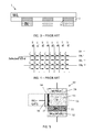
- a resistive memory array comprising a plurality of resistive memory elements, typically comprises a cross-bar array of top and bottom electrodes as illustrated schematically in FIG. 1 , in top view in FIG. 2 , and in cross-section in FIG.3 .
- the resistive memory device 1 comprises a plurality of top electrodes (e.g. word lines WL) and a plurality of bottom electrodes (e.g. bit lines BL) which, together with an active layer 2 between the top and bottom electrodes, form a plurality of cross-point memory elements.
- the active layer 2 is interposed between the plurality of word lines WL and bit lines BL.
- a programmable region i.e.
- a bit 3 is formed in the active layer 2.
- the resistivity of the bit 3 can be changed for example due to filament formation or filament disruption in response to a voltage or current applied between the corresponding word line WL and the bit line BL.
- the position of the filaments are schematically indicated with closed circles 4 in FIG. 2 . Supposing that the world lines WL and the bit lines BL each have a width F being the minimum width obtainable with a given technology, the density of the resistive memory device 1 as illustrated in FIG. 2 can be calculated to be 1 filament/4F 2 , thus 1 bit/4F 2 .
- raw cross-point arrays with single RRAM elements lead to a large parasitic current flowing through non-selected memory cells.
- raw cross-point arrays suffer from READ errors (sneak currents) and possibly from PROGRAM errors, as well as from excessive current and power consumption.
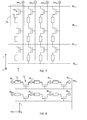
- selector 5 in each cell, as illustrated in FIG. 4 .
- this can be a transistor, requiring the addition of another control word line 6, but also a (bipolar) diode/switch device has been proposed as a selector 5.
- resistive memory arrays comprising memory cells including selection transistors are given in US2009/014836 .
- the present invention provides an integrated circuit having a resistivity switching memory, comprising a resistivity switching memory element, a first electrode associated with the resistivity switching memory element, a second electrode associated with the resistivity switching memory element, and a transistor device electrically coupled to the resistivity switching memory element.
- An inversion or accumulation channel of the transistor device is adapted for forming a switchable resistivity path, also called a virtual electrode, between the resistivity switching memory element and the second electrode.
- the transistor device may be any of a MOSFET, a pinch-off FET or a FinFET.
- the transistor device is a three-terminal device.
- the transistor device may include a channel area extending in a direction substantially perpendicular to a surface of a substrate onto which the resistivity switching memory is provided.
- no layer of material is present which can be conductive without being switched, hence e.g. no metallic layers are present between the resistivity switching memory element and the transistor device.
- the conductivity of the electrical path between the resistivity switching memory element and the electrode is controlled by the transistor device.
- the transistor device is configured to switch on and/or off the current between the resistivity switching memory element and the electrode.
- the present invention provides a resistive memory array comprising a plurality of integrated circuits as in any of the embodiments of the previous aspect.
- a resistive memory array may comprise a plurality of resistivity switching memory elements, a plurality of first electrodes each associated with at least one resistivity switching memory element, a plurality of second electrodes each associated with the at least one resistivity switching memory element, and a plurality of transistor devices, each transistor device being electrically coupled to one of the resistivity switching memory elements.
- An inversion or accumulation channel of a transistor device may be adapted for forming a switchable resistivity path between the electrically coupled resistivity switching memory element and the associated second electrode.
- the plurality of first electrodes may be arranged in a first direction, and a stack of first electrodes, resistivity switching memory elements, second electrodes and transistor devices may be arranged in a continuous stripe over a plurality of cells in the first direction.
- the plurality of transistor devices may be any of MOSFETs, pinch-off FETs or FinFETs.
- the plurality of resistivity switching memory elements may be arranged in a 3D stack.
- Such 3D stack may be formed of stripes of bitline-transistor-resistivity switching material stacks, which stripes are arranged adjacent one another but spaced apart from one another, overlaid with wordlines in a direction substantially perpendicular to the stripes of bitline stacks.
- the bitlines are all parallel to one another, and preferably the bitline stacks all have the same height and width.
- the plurality of resistivity switching memory elements may be logically arranged in rows and columns.
- the rows and columns may be substantially orthogonal to one another.
- the plurality of first electrodes may be arranged along the rows of the array.
- the wordlines may be arranged substantially perpendicular to the bitlines.
- the present invention provides a method of manufacturing a resistivity switching memory array (60).
- the method comprises providing a plurality of resistivity switching memory elements, providing a plurality of first electrodes and second electrodes each associated with at least one resistivity switching memory element, and providing a plurality of transistor devices each electrically coupled with at least one resistivity switching memory element.
- the transistor devices are adapted for each forming a switchable resistivity path between the resistivity switching memory element and one of the second electrodes.
- providing a plurality of resistivity switching memory elements may include providing resistivity switching memory elements in a 3D stack.
- Providing a plurality of first electrodes and second electrodes may comprise providing at least one layer of conductive material, and patterning the layer of conductive material.
- Providing a plurality of resistivity switching memory elements may comprise providing at least one layer of resistivity switching material and patterning the layer of resistivity switching material.
- Providing a plurality of transistor devices may comprise providing at least one layer of semiconductor material and patterning the layer of semiconductor material.
- patterning the layers of conductive material, resistivity switching material and semiconductor material may be performed in a single patterning step.
- the present invention provides a method of addressing a resistivity switching memory element in an array according to embodiments of the present invention.
- the method comprises selecting a first bitline and a second bitline associated with the resistivity switching memory element to be addressed, and selecting a transistor device associated with the resistivity switching memory element to be addressed, an inversion or accumulation channel of the transistor device thereby forming a conductive path between the resistivity switching memory element and the second electrode.
- Addressing may be any of programming or reading.
- BICS Bit Cost Scalable
- a non-volatile semiconductor memory to which the BICS technology is applied (hereinafter called BICS memory) has a feature in that it not only has a three-dimensional structure but also makes bit cost scalability possible so that a bit cost can be reduced in proportion to an increase of the number of stacked layers by devising a device structure and a process technology.
- a resistive random-access memory is a non-volatile memory type having as basic idea that a dielectric, which is normally insulating, can be made to conduct through a filament or conduction path formed after application of a sufficiently high voltage. Once the filament is formed, it may be reset (broken, resulting in high resistance) or set (reformed, resulting in lower resistance) by an appropriately applied voltage.
- a pure RRAM memory element is used as a basic memory cell, resulting in a configuration where parallel bitlines are crossed by perpendicular wordlines with the switching material placed between wordline and bitline at every cross-point.
- this architecture large parasitic currents flow through non-selected memory cells.
- an electrode is meant a layer of material which is intrinsically electrically conductive.
- a switchable electrode is meant a layer of material of which the electrical conductivity may be switched on or off e.g. when applying a voltage across or to that material.
- Such switchable electrode is also called a virtual electrode or a switchable resistivity path, i.e. an electrical path having switchable resistivity (high resistivity or low resistivity, whereby high resistivity means that in normal operating conditions substantially no electrical current flows, and low resistivity means that in normal operating conditions electrical current can flow).
- the present invention provides a resistivity switching memory cell 50.
- resistivity switching memory cell 50 comprises a resistivity switching memory element 51, for example, but not limited thereto, a HfO layer; a first electrode 52 associated with and located at a first side of the resistivity switching memory element 51, for example, but not limited thereto, a Hf electrode; and a second electrode 58 associated with and located at a second side of the resistivity switching memory element, opposite to the first side, for example, but not limited thereto, a Hf electrode.
- a transistor device 53 In between the resistivity switching memory element 51 and the second electrode 58, a transistor device 53 is provided, which is electrically coupled to the resistivity switching memory element 51.
- An inversion channel 54 of the transistor device 53 (or an accumulation channel in case the transistor device is a pinch-off FET) may be formed by appropriately switching the transistor device 53, this inversion or accumulation channel 54 being adapted for forming a switchable resistivity path.
- a suitable voltage may be applied over the resistivity switching memory element 51 for changing the resistivity of this element 51.
- the transistor device 53 includes a channel area 54 extending in a direction substantially perpendicular to a surface of a substrate onto which the resistive switching memory cell 50 is manufactured.
- the transistor device 53 may , for example be a FET (field-effect transistor), such as e.g. a pinch-off FET or a MOSFET.
- the transistor may be a vertical transistor, i.e. a transistor having it channel in a direction substantially perpendicular to the substrate onto which the transistor is provided.
- a transistor device 53 may be formed in a semiconductor layer 55, e.g. a silicon layer, on top of the resistivity switching layer 51.
- a gate electrode 56 is provided, sandwiching a gate dielectric 57 between the gate electrode 56 and the semiconductor layer 55.
- an inversion or accumulation channel 54 may be formed in the semiconductor layer 55.
- this inversion or accumulation channel 54 may be used as a switchable electrode between the resistivity switching memory element and the second electrode, for changing the content, i.e. a stored value, of the resistivity switching memory cell 50.
- the transistor device 53 is provided between the resistivity switching memory element 51 and the second electrode 58, and no other electrode is provided between the resistivity switching memory element 51 and the second electrode 58. This means that, in embodiments of the present invention, there may be a direct contact between the resistivity switching memory element 51 and the transistor device 53.
- the electrical path between the resistivity switching memory element 51 and the second electrode 58 is controlled by the transistor device 53.
- This transistor device 53 is configured to switch on and switch off the current between the resistivity switching memory element 51 and the second electrode 58.
- the type of transistor device used determines where the current path is provided, e.g. determines the width of the part of the semiconductor layer 55 where current can flow.
- the present invention provides a resistive memory array comprising a plurality of resistivity switching memory cells 50 in accordance with embodiments of the first aspect of the present invention.
- the array may be a 3D array, i.e. an array having a plurality of resistivity switching memory cells adjacent one another in a plane, and other resistivity switching memory elements laying in other planes substantially parallel with that plane.
- FIG. 6 schematically illustrates a top view of a portion of a resistive memory array 60 according to a particular embodiment of the present invention.
- the resistive memory array 60 comprises a plurality of resistive memory elements (not illustrated in FIG. 6 ) logically arranged in two dimensions in rows and columns (x and y), and in a third dimension (z) in layers. Rows and columns are arranged in a plane and form a layer of resistive memory elements. In accordance with embodiments of the present invention, different layers of resistive memory elements may be stacked on top of one another.
- FIG. 7 and FIG. 8 schematically illustrate a cross-section through a stack of such layers.
- the terms “horizontal” and “vertical” are used to provide a co-ordinate system in a layer, and for ease of explanation only. They do not need to, but may, refer to an actual physical direction of the device.
- the terms “column” and “row” are used to describe sets of array elements which are linked together.
- the linking can be in the form of a Cartesian array of rows and columns; however, the present invention is not limited thereto. As will be understood by those skilled in the art, columns and rows can be easily interchanged and it is intended in this disclosure that these terms be interchangeable. Also, non-Cartesian arrays may be constructed and are included within the scope of the invention.
- the terms “row” and “column” should be interpreted widely.
- the present disclosure refers to logically organized in rows and columns.
- sets of memory elements are linked together in a topologically linear intersecting manner; however, that the physical or topographical arrangement need not be so.
- the rows may be circles and the columns radii of these circles and the circles and radii are described in this invention as “logically organized” rows and columns.
- depth (related to the term “layer”) is used to provide another direction in the coordinate system defined by the terms “horizontal” and “vertical”.
- axes have been drawn in FIG. 6 , with x and ⁇ -axes along rows and columns, respectively, and z-axis along the depth direction.
- the resistive memory array 60 furthermore comprises a plurality of word lines WL i (in the embodiment illustrated 1 ⁇ i ⁇ 3, but in practical realizations i is often much larger than 3) arranged in the depth direction (z-direction) of the array of memory elements and wordlines arranged on a single column of memory elements (y-direction) being electrically connected to one another.
- the resistive memory array 60 further comprises a plurality of bit lines BL j (in the embodiment illustrated 1 ⁇ j ⁇ 4, but in practical realizations j is often much larger than 4) arranged in the direction of the rows of memory elements (x-direction). What cannot be seen in FIG. 6 but is clear from FIG. 7 , is that a plurality of bitlines are stacked on top of one another; at least a first and a second bitline, respectively connecting the first electrode 52 and the second electrode 58 of a memory cell 50 as illustrated in FGI. 5.
- the word lines WL i and the bit lines BL j are arranged in the form of a Cartesian array
- the word lines WL i are parallel to one another
- the bitlines BL j are parallel to one another.
- the word lines WL i may be arranged perpendicular to the bitlines BL j .
- the bitlines BL j may be arranged as concentric circles or as radii of such circles.
- Specific names of the various lines, e.g. word line and bit line are intended to be generic names used to facilitate the explanation and to refer to a particular function and this specific choice of words is not intended to in any way limit the invention. It should be understood that all these terms are used only to facilitate a better understanding of the specific structure being described, and are in no way intended to limit the invention.
- FIG. 7 illustrates a horizontal cross-section according to line VII-VII' in FIG. 6
- FIG. 8 illustrates a vertical cross-section according to line VIII-VIII' in FIG. 6
- FIG. 7 illustrates a layer of memory cells 70, at a particular level x.
- a plurality of bitlines BL x,j are provided in that layer x.
- Each memory cell 70 comprises a resistivity switching memory element 71 and a transistor device 72.
- a first electrode is electrically associated with the resistivity switching memory element 71, the first electrode being formed by a first bitline BL x,j adjacent the memory element 71, and a second electrode is electrically associated with the resistivity switching memory element 71, the second electrode being formed by a second bitline BL x,j+1 .
- An inversion or accumulation channel of the transistor device 72 is adapted for forming a switchable resistivity path between the resistivity switching memory element 71 and the second electrode. This switchable resistivity path may be switched to high resistivity or to low resistivity by appropriately controlling the transistor device 72.
- FIG. 8 illustrates a vertical cross-section along line VIII-VIII' through the array illustrated in FIG. 6 .
- Each layer comprises a plurality of bitlines BLz,j, where z refers to a particular layer in the stack, and j refers to a particular bitline in a layer.
- the wordlines when performing their function as wordline, i.e. when controlling the switching of the resistivity switching memory element 71, at the same time function as select lines for switching the transistor device 72, thus controlling the conductivity of the semiconductor layer 55 forming part of the transistor device 72 .
- a suitable voltage applied to the wordline WL in combination with the voltage applied to the two bitlines BL associated with the resistivity switching memory element 71, allows to switch or not switch the resistivity of the memory element 71.
- FIG. 12 A 3D cross-sectional view along line VII-VII' in FIG. 6 is illustrated in FIG. 12 .
- material layers are stacked in the depth direction (z-direction), which stacks run in bitline direction (also called the first direction in the context of the present invention, or the x-direction), thus forming a stripe of a material stack
- the stripes of material stacks are overlaid with wordlines WLi running in a direction substantially perpendicular to the first direction.
- the wordlines furthermore fill part of the space in depth direction, between two stripes of stacks of material in the 1 st direction. Neighboring wordlines in the x-direction are electrically insulated from one another.
- the present invention provides a method of manufacturing a resistivity switching memory array. Such method according to embodiments of the present invention is described hereinbelow.
- a substrate (not illustrated in the drawings) is provided.
- the term “substrate” may include any underlying material or materials that may be used, or upon which a device according to embodiments of the present invention may be formed.
- this "substrate” may include a semiconductor substrate such as e.g. a silicon, a gallium arsenide (GaAs), a gallium arsenide phosphide (GaAsP), an indium phosphide (InP), a germanium (Ge), or a silicon germanium (SiGe) substrate.
- a semiconductor substrate such as e.g. a silicon, a gallium arsenide (GaAs), a gallium arsenide phosphide (GaAsP), an indium phosphide (InP), a germanium (Ge), or a silicon germanium (SiGe) substrate.
- the "substrate” may include, for example, an insulating layer such as a SiO 2 or a Si 3 N 4 layer in addition to a semiconductor substrate portion.
- the term substrate also includes silicon-on-glass, silicon-on sapphire substrates.
- the term “substrate” is thus used to define generally the elements for layers that underlie a layer or portions of interest.
- the “substrate” may be any other base on which a layer is formed, for example a glass or metal layer.
- the substrate may be made of any suitable material, whether amorphous, polycrystalline or crystalline, such as LaAlO 3 , Si, TiN or other material.
- a plurality of layers are provided on or in a major surface of the substrate.
- the layers are a sequence of a layer of bitline material 90 (bottom electrode), an active layer 91 made of a material capable of having its resistivity changed in response to an electrical signal, and a layer of semiconductor material 92.
- Such stack of layers comprising a layer of bitline material 90, an active layer 91 and a layer of semiconductor material 92 may be stacked onto one another as many times as the number of layers required in the array.
- the layers of bitline material 90 may be made of conductive material, including metals, e.g. poly-silicon, TiSiC, C, TiW, SiC, Ti, V, W, Cr, Fe, Ni, Nb, Pd, Pt, Zr, Mo, Cu, Al, Ag, Au, Hf and alloys thereof; conductive oxides e.g. IrO 2 , RuO 2 , IrRuO 3 , LiNbO 3 ; metal nitrides, e.g. TiAlN, TiN, TaN, TiSiN, TiCN, TaSiN, MoN, TaAlN, WN; metal silicides e.g.
- the layer of bitline material may also be formed of a stack of one or more of these materials.
- the conductive material may be a material such as YBa 2 Cu 3 O 7 (YBCO) that allows the epitaxial growth of an overlying perovskite material.
- the layers of bitline material 90 may have a thickness in the range of between about 5 nm and about 500 nm.
- the layers of bitline material 90 may be made of the same material throughout the stack, or layers of different bitline material may be provided at different locations.
- the layers of bitline material 90 may have substantially the same thickness at different locations (different levels) in the stack, or different layers may have different thicknesses.
- the active layers 91 are deposited overlying the layers of bitline material 90.
- the active layers 91 are made of a material capable of having its resistivity changed in response to an electrical signal.
- the active material may be a metal oxide (binary oxides from transition metals as NiO, HfO, TaO, ZrO, AlO, NbO, TiO, ...), optionally with a metallic cap layer (Hf, Ti, Al, Zr, ...) on one side different from the side where the transistor resides, or complex oxides such as PrCaMnO (PCMO), or (doped) perovskite oxides, for example Cr:SrTi03, or it can be a solid electrolyte layer with incorporated Al or Cu, such as Cu(Al) Selenides or Tellerium compounds, or it can be combinations of multilayer stacks of different of the above layers combined.
- PCMO PrCaMnO
- Cu Cu(Al) Selenides or Tellerium compounds
- the active layers 91 can be phase change materials as e.g. GeSbTe, doped SbTe, or AsInSbTe.
- the active layers 91 may for example have a thickness between 5 nm and 500 nm.
- the active layers 91 can be deposited using any suitable deposition technique, including pulsed laser deposition, rf-sputtering, e-beam evaporation, thermal evaporation, atomic layer deposition, sol gel deposition, chemical vapor deposition.
- the active layer material is deposited over substantially the complete surface of the substrate, and is removed from outside the memory area by wet or dry etching or any other suitable process.
- the layers of semiconductor material 92 may be made of any type of semiconductor material capable of forming an inversion or accumulation channel if a suitable voltage is applied.
- the layers of semiconductor material can for example be layers of Si, polysilicon, Ge, SiGe, GaAs.
- the layers of semiconductor material may have a thickness between 5 and 50 nm.
- the layers of semiconductor material may be deposited by any suitable method, e.g. CVD (chemical vapor deposition), ALD (atomic layer deposition).
- At least one trench 93 is formed therethrough, in the direction of the bitlines (x-direction) so as to separate different bitlines from one another. This is illustrated in FIG. 9(b) .
- the trench 93 may be formed through the complete stack, i.e. down to the bottom of the stack.
- the trench 93 may be formed by etching, but finding the right etch chemistries might be difficult, as the stack to be etched might comprise materials which are difficult to etch. However, scaling of the structure is easy.
- a layer of dielectric material 100 may be applied inside the trench.
- the dielectric material may for example be SiO 2 or any other material suitable to function as a gate dielectric.
- the wordline material may be conductive material, including metals, e.g. poly-silicon, TiSiC, C, TiW, SiC, Ti, V, W, Cr, Fe, Ni, Nb, Pd, Pt, Zr, Mo, Cu, Al, Ag, Au, Hf and alloys thereof; conductive oxides e.g. IrO 2 , RuO 2 , IrRuO 3 , LiNbO 3 ; metal nitrides, e.g.
- FIG. 10(a) illustrates a side view of a structure in accordance with embodiments of the present invention
- FIG. 12 illustrates a 3D side view from the same structure, where no insulating material is provided between neighboring wordlines.
- a resistive memory array may be constructed by making stacks (in bitline direction) of bitlines, serving as bottom electrode for a resistive element, resistive elements, semiconducting material part of which may serve as the channel of a transistor device, e.g. a dual gate vertical flow fully depleted finFET device, and finally a second bitline, serving as top electrode.
- the wordlines are perpendicular to the bitlines and serve as gate electrodes for the above mentioned transistor devices.
- a method according to embodiments of the present invention has a significant advantage over prior art 3D stacking concepts: as there is no need for a complex stack between the bitlines (or between the wordlines) the minimum half-pitch of both bitlines and wordlines can theoretically be reduced down to 10 nm or below (while only requiring two lithography steps for an arbitrary number of stacked memory layers), so that it can be scaled to a very high memory density.
- a method for addressing, e.g. for programming or read-out, a resistivity switching memory element in an array according to the second aspect of the present invention.
- the method comprises selecting a particular wordline by putting an appropriate voltage level on that wordline. This induces the formation of induction channels in each of the semiconductor material layers adjacent the selected wordline.
- the method comprises selecting a first bitline and a second bitline, associated with the resistivity switching memory element to be addressed, by applying an appropriate electrical signal, e.g. voltage or current, to these bitlines. By applying these electrical signals to the bitlines, the resistivity of the resistivity switching memory element may be switched.
- a resistive element for example the resistive element indicated 91 in FIG. 11 can be driven from two sides, thus generating two inversion or accumulation channels 110 as illustrated in FIG. 11 .
- This provides increased storage capabilities, which may be expressed as smaller memories having a same storage capacity, or same sized memories having a larger storage capacity.
- the semiconductor material 92 between the two inversion or accumulation channels 110 serves as isolation layer in between such that the channels can be driven separately.
- a value (bit) may be stored independently in a single cell at either side of the resistivity switching memory material.
Landscapes
- Engineering & Computer Science (AREA)
- Chemical & Material Sciences (AREA)
- Materials Engineering (AREA)
- Manufacturing & Machinery (AREA)
- Crystallography & Structural Chemistry (AREA)
- Semiconductor Memories (AREA)
Abstract
Description
- The present invention relates to semiconductor memory devices, more particularly for example to arrays of non-volatile memory cells comprising a reversible resistance switching layer, their resistance value being representative of the data stored in the memory cell. The present invention in particular relates to a new array design for minimizing design area and to methods of fabrication thereof.
- A resistive memory device, such as for example the electrically programmable resistive cross point memory device as described in
US2003/0003674 , is a non-volatile memory device which generally comprises an active layer capable of having its resistivity changed in response to an electrical signal, interposed between a plurality of conductive top and bottom electrodes. The active layer usually comprises a dielectric material, such as for example one or more metal oxide layers, a solid electrolyte material, a magnetic tunnel junction of a phase change material, which may be interposed between two conductive electrodes, for example wire-shaped Pt-electrodes. At a cross point of a top electrode and a bottom electrode, a cross point referring to each position where a top electrode crosses a bottom electrode, the active layer has a programmable region with a resistivity that can change in response to an applied voltage. The memory effect of the resistive memory device lies in the programming of the memory device into two distinct resistive states. - A resistive memory array, comprising a plurality of resistive memory elements, typically comprises a cross-bar array of top and bottom electrodes as illustrated schematically in
FIG. 1 , in top view inFIG. 2 , and in cross-section inFIG.3 . Theresistive memory device 1 comprises a plurality of top electrodes (e.g. word lines WL) and a plurality of bottom electrodes (e.g. bit lines BL) which, together with anactive layer 2 between the top and bottom electrodes, form a plurality of cross-point memory elements. Theactive layer 2 is interposed between the plurality of word lines WL and bit lines BL. At each crossing of a word line WL with a bit line BL, a programmable region, i.e. abit 3, is formed in theactive layer 2. The resistivity of thebit 3 can be changed for example due to filament formation or filament disruption in response to a voltage or current applied between the corresponding word line WL and the bit line BL. The position of the filaments are schematically indicated with closedcircles 4 inFIG. 2 . Supposing that the world lines WL and the bit lines BL each have a width F being the minimum width obtainable with a given technology, the density of theresistive memory device 1 as illustrated inFIG. 2 can be calculated to be 1 filament/4F2, thus 1 bit/4F2. - Such raw cross-point arrays with single RRAM elements lead to a large parasitic current flowing through non-selected memory cells. Hence raw cross-point arrays suffer from READ errors (sneak currents) and possibly from PROGRAM errors, as well as from excessive current and power consumption.
- One solution to alleviate these problems is to put a
selector 5 in each cell, as illustrated inFIG. 4 . Ideally this can be a transistor, requiring the addition of anothercontrol word line 6, but also a (bipolar) diode/switch device has been proposed as aselector 5. Examples of resistive memory arrays comprising memory cells including selection transistors are given inUS2009/014836 . - Disadvantages of solutions including a
selector 5 in each cell are the increase of the cell size, hence the reduced memory density, the more complex processing - not a simple cross-point array but requiring the definition of intermediate pillar elements -, the fact that no appropriate 2 terminal bipolar selector devices have been identified. - Accordingly, there is room for new structures and processing methods for manufacturing non-volatile memory cells, which allow a high cell density.
- It is an object of embodiments of the present invention to provide high density non-volatile resistive memory arrays, for example 3D arrays.
- The above objective is accomplished by a method and device according to embodiments of the present invention.
- In one aspect, the present invention provides an integrated circuit having a resistivity switching memory, comprising a resistivity switching memory element, a first electrode associated with the resistivity switching memory element, a second electrode associated with the resistivity switching memory element, and a transistor device electrically coupled to the resistivity switching memory element. An inversion or accumulation channel of the transistor device is adapted for forming a switchable resistivity path, also called a virtual electrode, between the resistivity switching memory element and the second electrode. It is an advantage that such resistivity switching memories can easily be provided in an array structure. It is a further advantage that such resistivity switching memories can be placed close to one another, thus allowing high density memory devices to be created.
- In an integrated circuit according to embodiments of the present invention, the transistor device may be any of a MOSFET, a pinch-off FET or a FinFET. The transistor device is a three-terminal device.
- The transistor device may include a channel area extending in a direction substantially perpendicular to a surface of a substrate onto which the resistivity switching memory is provided.
- Advantageously, between the resistivity switching memory element and the transistor device no layer of material is present which can be conductive without being switched, hence e.g. no metallic layers are present between the resistivity switching memory element and the transistor device. The conductivity of the electrical path between the resistivity switching memory element and the electrode is controlled by the transistor device. The transistor device is configured to switch on and/or off the current between the resistivity switching memory element and the electrode.
- In a further aspect, the present invention provides a resistive memory array comprising a plurality of integrated circuits as in any of the embodiments of the previous aspect.
- A resistive memory array according to embodiments of the present invention may comprise a plurality of resistivity switching memory elements, a plurality of first electrodes each associated with at least one resistivity switching memory element, a plurality of second electrodes each associated with the at least one resistivity switching memory element, and a plurality of transistor devices, each transistor device being electrically coupled to one of the resistivity switching memory elements. An inversion or accumulation channel of a transistor device may be adapted for forming a switchable resistivity path between the electrically coupled resistivity switching memory element and the associated second electrode.
- In a resistive memory array according to embodiments of the present invention, the plurality of first electrodes may be arranged in a first direction, and a stack of first electrodes, resistivity switching memory elements, second electrodes and transistor devices may be arranged in a continuous stripe over a plurality of cells in the first direction.
- In advantageous embodiments of a resistive memory array according to embodiments of the present invention, the plurality of transistor devices may be any of MOSFETs, pinch-off FETs or FinFETs.
- In embodiments of the present invention, the plurality of resistivity switching memory elements may be arranged in a 3D stack. Such 3D stack may be formed of stripes of bitline-transistor-resistivity switching material stacks, which stripes are arranged adjacent one another but spaced apart from one another, overlaid with wordlines in a direction substantially perpendicular to the stripes of bitline stacks. The bitlines are all parallel to one another, and preferably the bitline stacks all have the same height and width.
- In a resistive memory array according to embodiments of the present invention, at least some of the plurality of resistivity switching memory elements may be logically arranged in rows and columns. The rows and columns may be substantially orthogonal to one another. The plurality of first electrodes may be arranged along the rows of the array. The wordlines may be arranged substantially perpendicular to the bitlines.
- In yet another aspect, the present invention provides a method of manufacturing a resistivity switching memory array (60). The method comprises providing a plurality of resistivity switching memory elements, providing a plurality of first electrodes and second electrodes each associated with at least one resistivity switching memory element, and providing a plurality of transistor devices each electrically coupled with at least one resistivity switching memory element. The transistor devices are adapted for each forming a switchable resistivity path between the resistivity switching memory element and one of the second electrodes.
- In a method according to embodiments of the present invention, providing a plurality of resistivity switching memory elements may include providing resistivity switching memory elements in a 3D stack.
- Providing a plurality of first electrodes and second electrodes may comprise providing at least one layer of conductive material, and patterning the layer of conductive material.
- Providing a plurality of resistivity switching memory elements may comprise providing at least one layer of resistivity switching material and patterning the layer of resistivity switching material.
- Providing a plurality of transistor devices may comprise providing at least one layer of semiconductor material and patterning the layer of semiconductor material.
- In particular embodiments, patterning the layers of conductive material, resistivity switching material and semiconductor material may be performed in a single patterning step.
- In still another embodiments, the present invention provides a method of addressing a resistivity switching memory element in an array according to embodiments of the present invention. The method comprises selecting a first bitline and a second bitline associated with the resistivity switching memory element to be addressed, and selecting a transistor device associated with the resistivity switching memory element to be addressed, an inversion or accumulation channel of the transistor device thereby forming a conductive path between the resistivity switching memory element and the second electrode. Addressing may be any of programming or reading.
- It is an advantage of embodiments of the present invention that cells with the smallest cell size in a raw cross-point array can be realized, thereby, however, reducing sneak currents compared to a prior art raw cross-point array, or even avoiding these.
- Particular and preferred aspects of the invention are set out in the accompanying independent and dependent claims. Features from the dependent claims may be combined with features of the independent claims and with features of other dependent claims as appropriate and not merely as explicitly set out in the claims.
- For purposes of summarizing the invention and the advantages achieved over the prior art, certain objects and advantages of the invention have been described herein above. Of course, it is to be understood that not necessarily all such objects or advantages may be achieved in accordance with any particular embodiment of the invention. Thus, for example, those skilled in the art will recognize that the invention may be embodied or carried out in a manner that achieves or optimizes one advantage or group of advantages as taught herein without necessarily achieving other objects or advantages as may be taught or suggested herein.
- The above and other aspects of the invention will be apparent from and elucidated with reference to the embodiment(s) described hereinafter.
- The invention will now be described further, by way of example, with reference to the accompanying drawings, in which:
-
FIG. 1 is a schematic illustration of a prior art resistive memory raw cross-point array with a cross-bar array configuration of the top electrodes and the bottom electrodes. -
FIG. 2 is a top view of a portion of a prior art resistive memory array as inFIG. 1 . -
FIG. 3 is a cross-sectional view of the portion of a prior art resistive memory array ofFIG. 2 , taken along section A-A inFIG. 2 . The shaded zones are the programmable regions in the active layer with changeable resistivity. -
FIG. 4 is a schematic illustration of a prior art resistive memory array including a selector in each memory cell. -
FIG. 5 is a schematic illustration of a resistivity switching memory cell according to embodiments of the present invention. -
FIG. 6 is a top view of a schematic illustration of orientation of wordlines and bitlines in an array according to embodiments of the present invention. -
FIG. 7 is a schematic cross-sectional view along bitlines of an array according to embodiments of the present invention. -
FIG. 8 is a schematic cross-sectional view along wordlines of an array according to embodiments of the present invention. -
FIG. 9 illustrates different layers deposited during a method of manufacturing an array according to embodiments of the present invention. -
FIG. 10 illustrates a further method step during manufacturing an array according to embodiments of the present invention, whereby wordlines have been provided. -
FIG. 11 illustrates formation of inversion or accumulation channels in memory cells in a array according to embodiments of the present invention. -
FIG. 12 is a schematic 3D illustration of part of a resistive memory array according to embodiments of the present invention. - The drawings are only schematic and are non-limiting. In the drawings, the size of some of the elements may be exaggerated and not drawn on scale for illustrative purposes. The dimensions and the relative dimensions do not necessarily correspond to actual reductions to practice of the invention.
- Any reference signs in the claims shall not be construed as limiting the scope.
- In the different drawings, the same reference signs refer to the same or analogous elements.
- The present invention will be described with respect to particular embodiments and with reference to certain drawings but the invention is not limited thereto but only by the claims.
- The terms first, second and the like in the description and in the claims, are used for distinguishing between similar elements and not necessarily for describing a sequence, either temporally, spatially, in ranking or in any other manner. It is to be understood that the terms so used are interchangeable under appropriate circumstances and that the embodiments of the invention described herein are capable of operation in other sequences than described or illustrated herein.
- Moreover, the terms top, under and the like in the description and the claims are used for descriptive purposes and not necessarily for describing relative positions. It is to be understood that the terms so used are interchangeable under appropriate circumstances and that the embodiments of the invention described herein are capable of operation in other orientations than described or illustrated herein.
- It is to be noticed that the term "comprising", used in the claims, should not be interpreted as being restricted to the means listed thereafter; it does not exclude other elements or steps. It is thus to be interpreted as specifying the presence of the stated features, integers, steps or components as referred to, but does not preclude the presence or addition of one or more other features, integers, steps or components, or groups thereof. Thus, the scope of the expression "a device comprising means A and B" should not be limited to devices consisting only of components A and B. It means that with respect to the present invention, the only relevant components of the device are A and B.
- Reference throughout this specification to "one embodiment" or "an embodiment" means that a particular feature, structure or characteristic described in connection with the embodiment is included in at least one embodiment of the present invention. Thus, appearances of the phrases "in one embodiment" or "in an embodiment" in various places throughout this specification are not necessarily all referring to the same embodiment, but may. Furthermore, the particular features, structures or characteristics may be combined in any suitable manner, as would be apparent to one of ordinary skill in the art from this disclosure, in one or more embodiments.
- Similarly it should be appreciated that in the description of exemplary embodiments of the invention, various features of the invention are sometimes grouped together in a single embodiment, figure, or description thereof for the purpose of streamlining the disclosure and aiding in the understanding of one or more of the various inventive aspects. This method of disclosure, however, is not to be interpreted as reflecting an intention that the claimed invention requires more features than are expressly recited in each claim. Rather, as the following claims reflect, inventive aspects lie in less than all features of a single foregoing disclosed embodiment. Thus, the claims following the detailed description are hereby expressly incorporated into this detailed description, with each claim standing on its own as a separate embodiment of this invention.
- Furthermore, while some embodiments described herein include some but not other features included in other embodiments, combinations of features of different embodiments are meant to be within the scope of the invention, and form different embodiments, as would be understood by those in the art. For example, in the following claims, any of the claimed embodiments can be used in any combination.
- It should be noted that the use of particular terminology when describing certain features or aspects of the invention should not be taken to imply that the terminology is being re-defined herein to be restricted to include any specific characteristics of the features or aspects of the invention with which that terminology is associated.
- In the description provided herein, numerous specific details are set forth. However, it is understood that embodiments of the invention may be practiced without these specific details. In other instances, well-known methods, structures and techniques have not been shown in detail in order not to obscure an understanding of this description.
- BICS (Bit Cost Scalable) technology is known as a technology for suppressing a bit cost of a semiconductor memory by increasing the capacity thereof by a three dimensional structure.
- A non-volatile semiconductor memory to which the BICS technology is applied (hereinafter called BICS memory) has a feature in that it not only has a three-dimensional structure but also makes bit cost scalability possible so that a bit cost can be reduced in proportion to an increase of the number of stacked layers by devising a device structure and a process technology.
- In the context of the present invention, a resistive random-access memory (RRAM) is a non-volatile memory type having as basic idea that a dielectric, which is normally insulating, can be made to conduct through a filament or conduction path formed after application of a sufficiently high voltage. Once the filament is formed, it may be reset (broken, resulting in high resistance) or set (reformed, resulting in lower resistance) by an appropriately applied voltage.
- In a raw cross-point cell, a pure RRAM memory element is used as a basic memory cell, resulting in a configuration where parallel bitlines are crossed by perpendicular wordlines with the switching material placed between wordline and bitline at every cross-point. In this architecture, large parasitic currents flow through non-selected memory cells.
- In the context of the present invention, with an electrode is meant a layer of material which is intrinsically electrically conductive. With a switchable electrode is meant a layer of material of which the electrical conductivity may be switched on or off e.g. when applying a voltage across or to that material. Such switchable electrode is also called a virtual electrode or a switchable resistivity path, i.e. an electrical path having switchable resistivity (high resistivity or low resistivity, whereby high resistivity means that in normal operating conditions substantially no electrical current flows, and low resistivity means that in normal operating conditions electrical current can flow).
- In a first aspect, the present invention provides a resistivity switching
memory cell 50. Such resistivity switchingmemory cell 50 according to embodiments of the present invention is illustrated inFIG. 5 . The resistivityswitching memory cell 50 comprises a resistivityswitching memory element 51, for example, but not limited thereto, a HfO layer; afirst electrode 52 associated with and located at a first side of the resistivityswitching memory element 51, for example, but not limited thereto, a Hf electrode; and asecond electrode 58 associated with and located at a second side of the resistivity switching memory element, opposite to the first side, for example, but not limited thereto, a Hf electrode. In between the resistivityswitching memory element 51 and thesecond electrode 58, atransistor device 53 is provided, which is electrically coupled to the resistivityswitching memory element 51. Aninversion channel 54 of the transistor device 53 (or an accumulation channel in case the transistor device is a pinch-off FET) may be formed by appropriately switching thetransistor device 53, this inversion oraccumulation channel 54 being adapted for forming a switchable resistivity path. By actuating thefirst electrode 52, thesecond electrode 58 and afurther electrode 56 so as to form the inversion oraccumulation channel 54, a suitable voltage may be applied over the resistivityswitching memory element 51 for changing the resistivity of thiselement 51. - In embodiments of the present invention, the
transistor device 53 includes achannel area 54 extending in a direction substantially perpendicular to a surface of a substrate onto which the resistiveswitching memory cell 50 is manufactured. Thetransistor device 53 may , for example be a FET (field-effect transistor), such as e.g. a pinch-off FET or a MOSFET. The transistor may be a vertical transistor, i.e. a transistor having it channel in a direction substantially perpendicular to the substrate onto which the transistor is provided. - A
transistor device 53 may be formed in asemiconductor layer 55, e.g. a silicon layer, on top of theresistivity switching layer 51. At a side of thesemiconductor layer 55, agate electrode 56 is provided, sandwiching agate dielectric 57 between thegate electrode 56 and thesemiconductor layer 55. By applying a suitable electrical signal to thegate electrode 56, an inversion oraccumulation channel 54 may be formed in thesemiconductor layer 55. In accordance with embodiments of the present invention, this inversion oraccumulation channel 54 may be used as a switchable electrode between the resistivity switching memory element and the second electrode, for changing the content, i.e. a stored value, of the resistivity switchingmemory cell 50. - In accordance with embodiments of the present invention, the
transistor device 53 is provided between the resistivityswitching memory element 51 and thesecond electrode 58, and no other electrode is provided between the resistivityswitching memory element 51 and thesecond electrode 58. This means that, in embodiments of the present invention, there may be a direct contact between the resistivityswitching memory element 51 and thetransistor device 53. - In accordance with embodiments of the present invention, the electrical path between the resistivity
switching memory element 51 and thesecond electrode 58 is controlled by thetransistor device 53. Thistransistor device 53 is configured to switch on and switch off the current between the resistivityswitching memory element 51 and thesecond electrode 58. The type of transistor device used determines where the current path is provided, e.g. determines the width of the part of thesemiconductor layer 55 where current can flow. - In a second aspect, the present invention provides a resistive memory array comprising a plurality of resistivity switching
memory cells 50 in accordance with embodiments of the first aspect of the present invention. The array may be a 3D array, i.e. an array having a plurality of resistivity switching memory cells adjacent one another in a plane, and other resistivity switching memory elements laying in other planes substantially parallel with that plane. -
FIG. 6 schematically illustrates a top view of a portion of aresistive memory array 60 according to a particular embodiment of the present invention. Theresistive memory array 60 comprises a plurality of resistive memory elements (not illustrated inFIG. 6 ) logically arranged in two dimensions in rows and columns (x and y), and in a third dimension (z) in layers. Rows and columns are arranged in a plane and form a layer of resistive memory elements. In accordance with embodiments of the present invention, different layers of resistive memory elements may be stacked on top of one another.FIG. 7 and FIG. 8 schematically illustrate a cross-section through a stack of such layers. Throughout this description, the terms "horizontal" and "vertical" (related to the terms "row" and "column" respectively) are used to provide a co-ordinate system in a layer, and for ease of explanation only. They do not need to, but may, refer to an actual physical direction of the device. Furthermore, the terms "column" and "row" are used to describe sets of array elements which are linked together. The linking can be in the form of a Cartesian array of rows and columns; however, the present invention is not limited thereto. As will be understood by those skilled in the art, columns and rows can be easily interchanged and it is intended in this disclosure that these terms be interchangeable. Also, non-Cartesian arrays may be constructed and are included within the scope of the invention. Accordingly the terms "row" and "column" should be interpreted widely. To facilitate in this wide interpretation, the present disclosure refers to logically organized in rows and columns. By this is meant that sets of memory elements are linked together in a topologically linear intersecting manner; however, that the physical or topographical arrangement need not be so. For example, the rows may be circles and the columns radii of these circles and the circles and radii are described in this invention as "logically organized" rows and columns. Moreover, throughout this description, the term "depth" (related to the term "layer") is used to provide another direction in the coordinate system defined by the terms "horizontal" and "vertical". For the ease of explanation, axes have been drawn inFIG. 6 , with x and γ-axes along rows and columns, respectively, and z-axis along the depth direction. - The
resistive memory array 60 furthermore comprises a plurality of word lines WLi (in the embodiment illustrated 1 ≤ i ≤ 3, but in practical realizations i is often much larger than 3) arranged in the depth direction (z-direction) of the array of memory elements and wordlines arranged on a single column of memory elements (y-direction) being electrically connected to one another. Theresistive memory array 60 further comprises a plurality of bit lines BLj (in the embodiment illustrated 1 ≤ j ≤ 4, but in practical realizations j is often much larger than 4) arranged in the direction of the rows of memory elements (x-direction). What cannot be seen inFIG. 6 but is clear fromFIG. 7 , is that a plurality of bitlines are stacked on top of one another; at least a first and a second bitline, respectively connecting thefirst electrode 52 and thesecond electrode 58 of amemory cell 50 as illustrated in FGI. 5. - In particular embodiments, where the word lines WLi and the bit lines BLj are arranged in the form of a Cartesian array, the word lines WLi are parallel to one another, and the bitlines BLj are parallel to one another. The word lines WLi may be arranged perpendicular to the bitlines BLj. In alternative embodiments, the bitlines BLj may be arranged as concentric circles or as radii of such circles. Specific names of the various lines, e.g. word line and bit line, are intended to be generic names used to facilitate the explanation and to refer to a particular function and this specific choice of words is not intended to in any way limit the invention. It should be understood that all these terms are used only to facilitate a better understanding of the specific structure being described, and are in no way intended to limit the invention.
- Schematic cross-sectional views of the array illustrated in
FIG. 6 are illustrated inFIG. 7 and FIG. 8 , whereFIG. 7 illustrates a horizontal cross-section according to line VII-VII' inFIG. 6 , andFIG. 8 illustrates a vertical cross-section according to line VIII-VIII' inFIG. 6 .
FIG. 7 illustrates a layer ofmemory cells 70, at a particular level x. A plurality of bitlines BLx,j are provided in that layer x. Eachmemory cell 70 comprises a resistivityswitching memory element 71 and atransistor device 72. A first electrode is electrically associated with the resistivityswitching memory element 71, the first electrode being formed by a first bitline BLx,j adjacent thememory element 71, and a second electrode is electrically associated with the resistivityswitching memory element 71, the second electrode being formed by a second bitline BLx,j+1. An inversion or accumulation channel of thetransistor device 72 is adapted for forming a switchable resistivity path between the resistivityswitching memory element 71 and the second electrode. This switchable resistivity path may be switched to high resistivity or to low resistivity by appropriately controlling thetransistor device 72.
FIG. 8 illustrates a vertical cross-section along line VIII-VIII' through the array illustrated inFIG. 6 .FIG. 8 illustrates a plurality of layers comprising memory cells according to embodiments of the present invention. Two layers are illustrated inFIG. 8 . Each layer comprises a plurality of bitlines BLz,j, where z refers to a particular layer in the stack, and j refers to a particular bitline in a layer. - It can be seen in the drawings, in particular in
FIG. 7 and FIG. 8 that the wordlines, when performing their function as wordline, i.e. when controlling the switching of the resistivityswitching memory element 71, at the same time function as select lines for switching thetransistor device 72, thus controlling the conductivity of thesemiconductor layer 55 forming part of thetransistor device 72 . A suitable voltage applied to the wordline WL, in combination with the voltage applied to the two bitlines BL associated with the resistivityswitching memory element 71, allows to switch or not switch the resistivity of thememory element 71. - A 3D cross-sectional view along line VII-VII' in
FIG. 6 is illustrated inFIG. 12 . It can be seen fromFIG. 12 that material layers are stacked in the depth direction (z-direction), which stacks run in bitline direction (also called the first direction in the context of the present invention, or the x-direction), thus forming a stripe of a material stack, The stripes of material stacks are overlaid with wordlines WLi running in a direction substantially perpendicular to the first direction. The wordlines furthermore fill part of the space in depth direction, between two stripes of stacks of material in the 1st direction. Neighboring wordlines in the x-direction are electrically insulated from one another. - In a third aspect, the present invention provides a method of manufacturing a resistivity switching memory array. Such method according to embodiments of the present invention is described hereinbelow.
- First, a substrate (not illustrated in the drawings) is provided. In embodiments of the present invention, the term "substrate" may include any underlying material or materials that may be used, or upon which a device according to embodiments of the present invention may be formed. In particular embodiments, this "substrate" may include a semiconductor substrate such as e.g. a silicon, a gallium arsenide (GaAs), a gallium arsenide phosphide (GaAsP), an indium phosphide (InP), a germanium (Ge), or a silicon germanium (SiGe) substrate. The "substrate" may include, for example, an insulating layer such as a SiO2 or a Si3N4 layer in addition to a semiconductor substrate portion. Thus, the term substrate also includes silicon-on-glass, silicon-on sapphire substrates. The term "substrate" is thus used to define generally the elements for layers that underlie a layer or portions of interest. Also, the "substrate" may be any other base on which a layer is formed, for example a glass or metal layer. As examples, the substrate may be made of any suitable material, whether amorphous, polycrystalline or crystalline, such as LaAlO3, Si, TiN or other material.
- On or in a major surface of the substrate, a plurality of layers are provided. The layers are a sequence of a layer of bitline material 90 (bottom electrode), an
active layer 91 made of a material capable of having its resistivity changed in response to an electrical signal, and a layer ofsemiconductor material 92. Such stack of layers comprising a layer ofbitline material 90, anactive layer 91 and a layer ofsemiconductor material 92 may be stacked onto one another as many times as the number of layers required in the array. - The layers of
bitline material 90 may be made of conductive material, including metals, e.g. poly-silicon, TiSiC, C, TiW, SiC, Ti, V, W, Cr, Fe, Ni, Nb, Pd, Pt, Zr, Mo, Cu, Al, Ag, Au, Hf and alloys thereof; conductive oxides e.g. IrO2, RuO2, IrRuO3, LiNbO3; metal nitrides, e.g. TiAlN, TiN, TaN, TiSiN, TiCN, TaSiN, MoN, TaAlN, WN; metal silicides e.g. TiSix, NiSix, CoSix; or combinations of any of the above. The layer of bitline material may also be formed of a stack of one or more of these materials. In particular embodiments, the conductive material may be a material such as YBa2Cu3O7 (YBCO) that allows the epitaxial growth of an overlying perovskite material. The layers ofbitline material 90 may have a thickness in the range of between about 5 nm and about 500 nm. The layers ofbitline material 90 may be made of the same material throughout the stack, or layers of different bitline material may be provided at different locations. The layers ofbitline material 90 may have substantially the same thickness at different locations (different levels) in the stack, or different layers may have different thicknesses. - The
active layers 91 are deposited overlying the layers ofbitline material 90. Theactive layers 91 are made of a material capable of having its resistivity changed in response to an electrical signal. The active material may be a metal oxide (binary oxides from transition metals as NiO, HfO, TaO, ZrO, AlO, NbO, TiO, ...), optionally with a metallic cap layer (Hf, Ti, Al, Zr, ...) on one side different from the side where the transistor resides, or complex oxides such as PrCaMnO (PCMO), or (doped) perovskite oxides, for example Cr:SrTi03, or it can be a solid electrolyte layer with incorporated Al or Cu, such as Cu(Al) Selenides or Tellerium compounds, or it can be combinations of multilayer stacks of different of the above layers combined. Alternatively, it can be phase change materials as e.g. GeSbTe, doped SbTe, or AsInSbTe. Theactive layers 91 may for example have a thickness between 5 nm and 500 nm. Theactive layers 91 can be deposited using any suitable deposition technique, including pulsed laser deposition, rf-sputtering, e-beam evaporation, thermal evaporation, atomic layer deposition, sol gel deposition, chemical vapor deposition. The active layer material is deposited over substantially the complete surface of the substrate, and is removed from outside the memory area by wet or dry etching or any other suitable process. - The layers of
semiconductor material 92 may be made of any type of semiconductor material capable of forming an inversion or accumulation channel if a suitable voltage is applied. The layers of semiconductor material can for example be layers of Si, polysilicon, Ge, SiGe, GaAs. The layers of semiconductor material may have a thickness between 5 and 50 nm. The layers of semiconductor material may be deposited by any suitable method, e.g. CVD (chemical vapor deposition), ALD (atomic layer deposition). - Once the stack has been created, at least one
trench 93 is formed therethrough, in the direction of the bitlines (x-direction) so as to separate different bitlines from one another. This is illustrated inFIG. 9(b) . Thetrench 93 may be formed through the complete stack, i.e. down to the bottom of the stack. Thetrench 93 may be formed by etching, but finding the right etch chemistries might be difficult, as the stack to be etched might comprise materials which are difficult to etch. However, scaling of the structure is easy. - As can be seen in
FIG. 10(b) , a layer ofdielectric material 100 may be applied inside the trench. The dielectric material may for example be SiO2 or any other material suitable to function as a gate dielectric. - Over the layer of
dielectric material 100, a layer ofwordline material 101 is provided, filling thetrench 93. The wordline material may be conductive material, including metals, e.g. poly-silicon, TiSiC, C, TiW, SiC, Ti, V, W, Cr, Fe, Ni, Nb, Pd, Pt, Zr, Mo, Cu, Al, Ag, Au, Hf and alloys thereof; conductive oxides e.g. IrO2, RuO2, IrRuO3, LiNbO3; metal nitrides, e.g. TiAlN, TiN, TaN, TiSiN, TiCN, TaSiN, MoN, TaAlN, WN; metal silicides e.g. TiSix, NiSix, CoSix; or combinations of any of the above.. After filling thetrenches 93 with wordline material, this wordline material is patterned and removed from locations where no wordline material should be present. Optionally, the freed spaces between the wordlines in theformer trenches 93 may be filled with insulating material.FIG. 10(a) illustrates a side view of a structure in accordance with embodiments of the present invention, andFIG. 12 illustrates a 3D side view from the same structure, where no insulating material is provided between neighboring wordlines. - It is clear from the above that a resistive memory array according to embodiments of the present invention may be constructed by making stacks (in bitline direction) of bitlines, serving as bottom electrode for a resistive element, resistive elements, semiconducting material part of which may serve as the channel of a transistor device, e.g. a dual gate vertical flow fully depleted finFET device, and finally a second bitline, serving as top electrode. The wordlines are perpendicular to the bitlines and serve as gate electrodes for the above mentioned transistor devices.
- A method according to embodiments of the present invention has a significant advantage over prior art 3D stacking concepts: as there is no need for a complex stack between the bitlines (or between the wordlines) the minimum half-pitch of both bitlines and wordlines can theoretically be reduced down to 10 nm or below (while only requiring two lithography steps for an arbitrary number of stacked memory layers), so that it can be scaled to a very high memory density.
- In a fourth aspect, a method is provided for addressing, e.g. for programming or read-out, a resistivity switching memory element in an array according to the second aspect of the present invention. The method comprises selecting a particular wordline by putting an appropriate voltage level on that wordline. This induces the formation of induction channels in each of the semiconductor material layers adjacent the selected wordline. Furthermore, the method comprises selecting a first bitline and a second bitline, associated with the resistivity switching memory element to be addressed, by applying an appropriate electrical signal, e.g. voltage or current, to these bitlines. By applying these electrical signals to the bitlines, the resistivity of the resistivity switching memory element may be switched.
- It is an advantage of embodiments of the present invention that a resistive element, for example the resistive element indicated 91 in
FIG. 11 can be driven from two sides, thus generating two inversion oraccumulation channels 110 as illustrated inFIG. 11 . This provides increased storage capabilities, which may be expressed as smaller memories having a same storage capacity, or same sized memories having a larger storage capacity. Thesemiconductor material 92 between the two inversion oraccumulation channels 110 serves as isolation layer in between such that the channels can be driven separately. A value (bit) may be stored independently in a single cell at either side of the resistivity switching memory material. - While the invention has been illustrated and described in detail in the drawings and foregoing description, such illustration and description are to be considered illustrative or exemplary and not restrictive. The foregoing description details certain embodiments of the invention. It will be appreciated, however, that no matter how detailed the foregoing appears in text, the invention may be practiced in many ways. The invention is not limited to the disclosed embodiments, but only by the claims.
Claims (15)
- An integrated circuit having a resistivity switching memory (50), comprising a resistivity switching memory element (51),
a first electrode (52) associated with the resistivity switching memory element (51),
a second electrode (58) associated with the resistivity switching memory element (51), and
a transistor device (53) electrically coupled to the resistivity switching memory element (51), wherein an inversion or accumulation channel (54) of the transistor device (53) is adapted for forming a switchable resistivity path between the resistivity switching memory element and the second electrode. - An integrated circuit according to claim 1, wherein the transistor device (53) is any of a MOSFET, a pinch-off FET or a FinFET.
- An integrated circuit according to any of the previous claims, wherein the transistor device (53) includes a channel area extending in a direction substantially perpendicular to a surface of a substrate onto which the resistivity switching memory (50) is provided.
- An integrated circuit according to any of the previous claims, wherein between the resistivity switching memory element (51) and the transistor device (53) no layer of material is present which can be conductive without being switched.
- A resistive memory array (60), comprising
a plurality of resistivity switching memory elements (71),
a plurality of first electrodes (BLi) each associated with at least one resistivity switching memory element (71),
a plurality of second electrodes (BLi+1) each associated with the at least one resistivity switching memory element (71), and
a plurality of transistor devices (72), each transistor device (72) being electrically coupled to one of the resistivity switching memory elements (71),
wherein an inversion or accumulation channel of a transistor device (72) is adapted for forming a switchable resistivity path between the electrically coupled resistivity switching memory element and the associated second electrode. - A resistive memory array (60) according to claim 5, the plurality of first electrodes (BLi) being arranged in a first direction, wherein a stack of first electrodes (BLi), resistivity switching memory elements (71), second electrodes (BLi+1) and transistor devices (72) are arranged in a continuous stripe in the first direction.
- A resistive memory array (60) according to any of claims 5 or 6, wherein the plurality of transistor devices (72) are any of MOSFETs or pinch-off FETs or FinFETs.
- A resistive memory array (60) according to any of claims 5 to 7, wherein the plurality of resistivity switching memory elements (71) are arranged in a 3D stack.
- A resistive memory array (60) according to any of claims 5 to 8, wherein the wordlines are arranged substantially perpendicular to the bitlines.
- A method of manufacturing a resistivity switching memory array (60), comprising providing a plurality of resistivity switching memory elements (70),
providing a plurality of first electrodes (BLi) and second electrodes (BLi+1) each associated with at least one resistivity switching memory element (70), and
providing a plurality of transistor devices (72) each electrically coupled with at least one resistivity switching memory element (70),
wherein the transistor devices (72) are adapted for each forming a switchable resistivity path between the resistivity switching memory element (70) and one of the second electrodes (BLi+1). - A method according to claim 10, wherein providing a plurality of resistivity switching memory elements (70) includes providing resistivity switching memory elements in a 3D stack.
- A method according to any of claims 10 or 11, wherein providing a plurality of first electrodes (BLi) and second electrodes (BLi+1) comprises providing at least one layer of conductive material (90), and patterning the layer of conductive material (90).
- A method according to any of claims 10 to 12, wherein providing a plurality of transistor devices (72) comprises providing at least one layer of semiconductor material (92) and patterning the layer of semiconductor material (92).
- A method according to any of claims 12 or 13, the method further including providing at least one layer of resistivity switching material (91) and patterning the layer of resistivity switching material (91), wherein patterning the layers of conductive material (90), resistivity switching material (91) and semiconductor material (92) is performed in a single patterning step.
- A method of addressing a resistivity switching memory element in an array according to any of claims 5 to 9, comprising
selecting a first bitline (BLi) and a second bitline (BLi+1) associated with the resistivity switching memory element to be addressed, and
selecting a transistor device (72) associated with the resistivity switching memory element to be addressed, an inversion or accumulation channel of the transistor device (72) thereby forming a conductive path between the resistivity switching memory element and the second electrode.
Priority Applications (3)
| Application Number | Priority Date | Filing Date | Title |
|---|---|---|---|
| EP11195473.1A EP2608210B1 (en) | 2011-12-23 | 2011-12-23 | Stacked RRAM array with integrated transistor selector |
| US13/723,164 US9972386B2 (en) | 2011-12-23 | 2012-12-20 | Stacked RRAM array with integrated transistor selector |
| JP2012279876A JP6230229B2 (en) | 2011-12-23 | 2012-12-21 | Stacked RRAM with integrated transistor selector |
Applications Claiming Priority (1)
| Application Number | Priority Date | Filing Date | Title |
|---|---|---|---|
| EP11195473.1A EP2608210B1 (en) | 2011-12-23 | 2011-12-23 | Stacked RRAM array with integrated transistor selector |
Publications (2)
| Publication Number | Publication Date |
|---|---|
| EP2608210A1 true EP2608210A1 (en) | 2013-06-26 |
| EP2608210B1 EP2608210B1 (en) | 2019-04-17 |
Family
ID=45440300
Family Applications (1)
| Application Number | Title | Priority Date | Filing Date |
|---|---|---|---|
| EP11195473.1A Active EP2608210B1 (en) | 2011-12-23 | 2011-12-23 | Stacked RRAM array with integrated transistor selector |
Country Status (3)
| Country | Link |
|---|---|
| US (1) | US9972386B2 (en) |
| EP (1) | EP2608210B1 (en) |
| JP (1) | JP6230229B2 (en) |
Cited By (2)
| Publication number | Priority date | Publication date | Assignee | Title |
|---|---|---|---|---|
| WO2016140715A1 (en) * | 2015-03-02 | 2016-09-09 | Sandisk Technologies Llc | Parallel bit line three-dimensional resistive random access memory |
| CN113078257A (en) * | 2020-01-03 | 2021-07-06 | 华邦电子股份有限公司 | Resistive random access memory and manufacturing method thereof |
Families Citing this family (15)
| Publication number | Priority date | Publication date | Assignee | Title |
|---|---|---|---|---|
| US9793255B2 (en) | 2013-01-31 | 2017-10-17 | Infineon Technologies Ag | Power semiconductor device including a cooling material |
| US9117748B2 (en) * | 2013-01-31 | 2015-08-25 | Infineon Technologies Ag | Semiconductor device including a phase change material |
| US9343317B2 (en) | 2013-07-01 | 2016-05-17 | Micron Technology, Inc. | Methods of forming silicon-containing dielectric materials and semiconductor device structures |
| US10079283B2 (en) | 2014-07-17 | 2018-09-18 | E Ink Holdings Inc. | Manufacturing method of a transistor |
| US10109346B2 (en) | 2014-07-30 | 2018-10-23 | Hewlett Packard Enterprise Development Lp | Apparatus having a memory cell and a shunt device |
| US9911693B2 (en) * | 2015-08-28 | 2018-03-06 | Micron Technology, Inc. | Semiconductor devices including conductive lines and methods of forming the semiconductor devices |
| US9953705B2 (en) | 2016-04-26 | 2018-04-24 | Western Digital Technologies, Inc. | Planar memory cell architectures in resistive memory devices |
| US20170316824A1 (en) * | 2016-04-29 | 2017-11-02 | HGST Netherlands B.V. | Multi-layer resistive memory devices |
| US10020346B2 (en) | 2016-05-23 | 2018-07-10 | Western Digital Technologies, Inc. | Resistive memory device by substrate reduction |
| US10269869B1 (en) | 2017-11-30 | 2019-04-23 | International Business Machines Corporation | High-density field-enhanced ReRAM integrated with vertical transistors |
| JP6829733B2 (en) | 2019-01-16 | 2021-02-10 | ウィンボンド エレクトロニクス コーポレーション | Random access memory with variable resistance |
| US11037986B2 (en) | 2019-06-19 | 2021-06-15 | International Business Machines Corporation | Stacked resistive memory with individual switch control |
| US11164907B2 (en) | 2020-03-11 | 2021-11-02 | International Business Machines Corporation | Resistive random access memory integrated with stacked vertical transistors |
| US11482571B2 (en) | 2020-06-23 | 2022-10-25 | Taiwan Semiconductor Manufacturing Company, Ltd. | Memory array with asymmetric bit-line architecture |
| US11903221B2 (en) * | 2020-08-17 | 2024-02-13 | Taiwan Semiconductor Manufacturing Co., Ltd. | Three dimensional semiconductor device with memory stack |
Citations (2)
| Publication number | Priority date | Publication date | Assignee | Title |
|---|---|---|---|---|
| US20100208509A1 (en) * | 2009-02-19 | 2010-08-19 | Kabushiki Kaisha Toshiba | Nonvolatile semiconductor memory device, and production method thereof |
| US20110068409A1 (en) * | 2009-09-22 | 2011-03-24 | Samsung Electronics Co., Ltd. | Resistive memory devices including vertical transistor arrays and related fabrication methods |
Family Cites Families (21)
| Publication number | Priority date | Publication date | Assignee | Title |
|---|---|---|---|---|
| US6531371B2 (en) | 2001-06-28 | 2003-03-11 | Sharp Laboratories Of America, Inc. | Electrically programmable resistance cross point memory |
| US6819583B2 (en) | 2003-01-15 | 2004-11-16 | Sharp Laboratories Of America, Inc. | Ferroelectric resistor non-volatile memory array |
| US7009278B2 (en) * | 2003-11-24 | 2006-03-07 | Sharp Laboratories Of America, Inc. | 3d rram |
| KR101213702B1 (en) * | 2006-04-21 | 2012-12-18 | 삼성전자주식회사 | Non-volatile memory device having a pair of fins between which a void is defined |
| US7763932B2 (en) * | 2006-06-29 | 2010-07-27 | International Business Machines Corporation | Multi-bit high-density memory device and architecture and method of fabricating multi-bit high-density memory devices |
| US7359226B2 (en) * | 2006-08-28 | 2008-04-15 | Qimonda Ag | Transistor, memory cell array and method for forming and operating a memory device |
| JP2008078404A (en) * | 2006-09-21 | 2008-04-03 | Toshiba Corp | Semiconductor memory and manufacturing method thereof |
| JP5159116B2 (en) * | 2007-02-07 | 2013-03-06 | 株式会社東芝 | Semiconductor memory device |
| US7539039B2 (en) | 2007-02-28 | 2009-05-26 | Qimonda Ag | Integrated circuit having a resistive switching device |
| US7663134B2 (en) | 2007-07-10 | 2010-02-16 | Taiwan Semiconductor Manufacturing Company, Ltd. | Memory array with a selector connected to multiple resistive cells |
| US20090034355A1 (en) | 2007-07-30 | 2009-02-05 | Qimonda Ag | Integrated circuit including memory cells with tunnel fet as selection transistor |
| US8665629B2 (en) | 2007-09-28 | 2014-03-04 | Qimonda Ag | Condensed memory cell structure using a FinFET |
| JP2009117003A (en) * | 2007-11-09 | 2009-05-28 | Toshiba Corp | Method for reading data in nonvolatile memory device |
| WO2010076833A1 (en) | 2008-12-31 | 2010-07-08 | Fabio Pellizzer | Word-line driver including pull-up resistor and pull-down transistor |
| US8153488B2 (en) * | 2009-03-24 | 2012-04-10 | Kabushiki Kaisha Toshiba | Method for manufacturing nonvolatile storage device |
| JP5388814B2 (en) * | 2009-11-24 | 2014-01-15 | 株式会社東芝 | Semiconductor memory device |
| JP5450165B2 (en) * | 2010-02-26 | 2014-03-26 | 株式会社東芝 | Nonvolatile semiconductor memory device and method of manufacturing nonvolatile semiconductor memory device |
| JP5641779B2 (en) * | 2010-05-18 | 2014-12-17 | 株式会社日立製作所 | Nonvolatile memory device and manufacturing method thereof |
| JP5054803B2 (en) * | 2010-05-26 | 2012-10-24 | シャープ株式会社 | Semiconductor memory device |
| JP5508944B2 (en) * | 2010-06-08 | 2014-06-04 | 株式会社東芝 | Semiconductor memory device |
| JP2013069753A (en) * | 2011-09-21 | 2013-04-18 | Toshiba Corp | Semiconductor storage device and manufacturing method of the same |
-
2011
- 2011-12-23 EP EP11195473.1A patent/EP2608210B1/en active Active
-
2012
- 2012-12-20 US US13/723,164 patent/US9972386B2/en active Active
- 2012-12-21 JP JP2012279876A patent/JP6230229B2/en active Active
Patent Citations (2)
| Publication number | Priority date | Publication date | Assignee | Title |
|---|---|---|---|---|
| US20100208509A1 (en) * | 2009-02-19 | 2010-08-19 | Kabushiki Kaisha Toshiba | Nonvolatile semiconductor memory device, and production method thereof |
| US20110068409A1 (en) * | 2009-09-22 | 2011-03-24 | Samsung Electronics Co., Ltd. | Resistive memory devices including vertical transistor arrays and related fabrication methods |
Non-Patent Citations (1)
| Title |
|---|
| WANG C-H ET AL: "Three-dimensional 4F<2> ReRAM with vertical BJT driver by CMOS logic compatible process", IEEE TRANSACTIONS ON ELECTRON DEVICES - SPECIAL ISSUE ON CHARACTERIZATION OF NANO CMOS VARIABILITY BY SIMULATION AND MEASUREMENTS AUGUST 2011 INSTITUTE OF ELECTRICAL AND ELECTRONICS ENGINEERS INC. USA, vol. 58, no. 8, August 2011 (2011-08-01), pages 2466 - 2472, XP002676124, DOI: 10.1109/TED.2011.2157928 * |
Cited By (4)
| Publication number | Priority date | Publication date | Assignee | Title |
|---|---|---|---|---|
| WO2016140715A1 (en) * | 2015-03-02 | 2016-09-09 | Sandisk Technologies Llc | Parallel bit line three-dimensional resistive random access memory |
| US9698202B2 (en) | 2015-03-02 | 2017-07-04 | Sandisk Technologies Llc | Parallel bit line three-dimensional resistive random access memory |
| CN113078257A (en) * | 2020-01-03 | 2021-07-06 | 华邦电子股份有限公司 | Resistive random access memory and manufacturing method thereof |
| CN113078257B (en) * | 2020-01-03 | 2023-09-12 | 华邦电子股份有限公司 | Resistive random access memory and manufacturing method thereof |
Also Published As
| Publication number | Publication date |
|---|---|
| US20130161583A1 (en) | 2013-06-27 |
| US9972386B2 (en) | 2018-05-15 |
| EP2608210B1 (en) | 2019-04-17 |
| JP6230229B2 (en) | 2017-11-15 |
| JP2013138203A (en) | 2013-07-11 |
Similar Documents
| Publication | Publication Date | Title |
|---|---|---|
| US9972386B2 (en) | Stacked RRAM array with integrated transistor selector | |
| EP3178113B1 (en) | Fully isolated selector for memory device | |
| US9812505B2 (en) | Non-volatile memory device containing oxygen-scavenging material portions and method of making thereof | |
| US10580979B2 (en) | Memory device and method of manufacturing the same | |
| KR101880339B1 (en) | Three dimensional non-volatile storage with interleaved vertical select devices above and below vertical bit lines | |
| KR101230874B1 (en) | Nonvolatile memory cell comprising switchable resistor and transistor | |
| US9312479B2 (en) | Variable resistance memory device | |
| US20130210211A1 (en) | Vertical Cross-Point Memory Arrays | |
| US20130170283A1 (en) | Low forming voltage non-volatile storage device | |
| KR20180109287A (en) | Memory device | |
| CN101685827A (en) | Storage device and manufacturing method thereof | |
| US9236122B2 (en) | Shared-gate vertical-TFT for vertical bit line array | |
| US20220293680A1 (en) | Variable resistance memory device | |
| KR101202199B1 (en) | 3-dimensional resistance change memory device, resistance change memory device array, and electronic product including the device | |
| CN112243527A (en) | Phase change memory device with wire threshold switching selector and method of forming the same | |
| EP2544239A1 (en) | Memory cell and method for manufacturing | |
| KR101481920B1 (en) | Using metal-insulator transition selection device and nonvolatile memory cell including the same | |
| KR101088487B1 (en) | Method for manufacturing resistance change memory device array, electronics and device array with selection device and 3D structure resistance change memory device | |
| KR100993052B1 (en) | A resistive change memory device, a resistive change memory device array, an electronic product, and a manufacturing method of the device having a three-dimensional structure | |
| EP2608209A1 (en) | Resistive memory array | |
| KR20250020085A (en) | Resistance variable memory device | |
| KR101127251B1 (en) | Highly integrated non-volatile memory and the manufacturing method thereof | |
| KR20230083098A (en) | Variable resistance memory device | |
| CN112602152A (en) | Memory device having memory cells with multiple threshold voltages and methods of forming and operating the same |
Legal Events
| Date | Code | Title | Description |
|---|---|---|---|
| AK | Designated contracting states |
Kind code of ref document: A1 Designated state(s): AL AT BE BG CH CY CZ DE DK EE ES FI FR GB GR HR HU IE IS IT LI LT LU LV MC MK MT NL NO PL PT RO RS SE SI SK SM TR |
|
| AX | Request for extension of the european patent |
Extension state: BA ME |
|
| PUAI | Public reference made under article 153(3) epc to a published international application that has entered the european phase |
Free format text: ORIGINAL CODE: 0009012 |
|
| 17P | Request for examination filed |
Effective date: 20131226 |
|
| RBV | Designated contracting states (corrected) |
Designated state(s): AL AT BE BG CH CY CZ DE DK EE ES FI FR GB GR HR HU IE IS IT LI LT LU LV MC MK MT NL NO PL PT RO RS SE SI SK SM TR |
|
| STAA | Information on the status of an ep patent application or granted ep patent |
Free format text: STATUS: EXAMINATION IS IN PROGRESS |
|
| 17Q | First examination report despatched |
Effective date: 20171115 |
|
| RAP1 | Party data changed (applicant data changed or rights of an application transferred) |
Owner name: IMEC VZW |
|
| GRAP | Despatch of communication of intention to grant a patent |
Free format text: ORIGINAL CODE: EPIDOSNIGR1 |
|
| STAA | Information on the status of an ep patent application or granted ep patent |
Free format text: STATUS: GRANT OF PATENT IS INTENDED |
|
| RIC1 | Information provided on ipc code assigned before grant |
Ipc: H01L 27/24 20060101ALI20181002BHEP Ipc: G11C 13/00 20060101AFI20181002BHEP Ipc: H01L 45/00 20060101ALI20181002BHEP |
|
| INTG | Intention to grant announced |
Effective date: 20181029 |
|
| GRAS | Grant fee paid |
Free format text: ORIGINAL CODE: EPIDOSNIGR3 |
|
| GRAA | (expected) grant |
Free format text: ORIGINAL CODE: 0009210 |
|
| STAA | Information on the status of an ep patent application or granted ep patent |
Free format text: STATUS: THE PATENT HAS BEEN GRANTED |
|
| AK | Designated contracting states |
Kind code of ref document: B1 Designated state(s): AL AT BE BG CH CY CZ DE DK EE ES FI FR GB GR HR HU IE IS IT LI LT LU LV MC MK MT NL NO PL PT RO RS SE SI SK SM TR |
|
| REG | Reference to a national code |
Ref country code: GB Ref legal event code: FG4D |
|
| REG | Reference to a national code |
Ref country code: CH Ref legal event code: EP |
|
| REG | Reference to a national code |
Ref country code: DE Ref legal event code: R096 Ref document number: 602011058105 Country of ref document: DE |
|
| REG | Reference to a national code |
Ref country code: AT Ref legal event code: REF Ref document number: 1122442 Country of ref document: AT Kind code of ref document: T Effective date: 20190515 Ref country code: IE Ref legal event code: FG4D |
|
| REG | Reference to a national code |
Ref country code: NL Ref legal event code: MP Effective date: 20190417 |
|
| REG | Reference to a national code |
Ref country code: LT Ref legal event code: MG4D |
|
| PG25 | Lapsed in a contracting state [announced via postgrant information from national office to epo] |
Ref country code: NL Free format text: LAPSE BECAUSE OF FAILURE TO SUBMIT A TRANSLATION OF THE DESCRIPTION OR TO PAY THE FEE WITHIN THE PRESCRIBED TIME-LIMIT Effective date: 20190417 |
|
| PG25 | Lapsed in a contracting state [announced via postgrant information from national office to epo] |
Ref country code: ES Free format text: LAPSE BECAUSE OF FAILURE TO SUBMIT A TRANSLATION OF THE DESCRIPTION OR TO PAY THE FEE WITHIN THE PRESCRIBED TIME-LIMIT Effective date: 20190417 Ref country code: LT Free format text: LAPSE BECAUSE OF FAILURE TO SUBMIT A TRANSLATION OF THE DESCRIPTION OR TO PAY THE FEE WITHIN THE PRESCRIBED TIME-LIMIT Effective date: 20190417 Ref country code: HR Free format text: LAPSE BECAUSE OF FAILURE TO SUBMIT A TRANSLATION OF THE DESCRIPTION OR TO PAY THE FEE WITHIN THE PRESCRIBED TIME-LIMIT Effective date: 20190417 Ref country code: SE Free format text: LAPSE BECAUSE OF FAILURE TO SUBMIT A TRANSLATION OF THE DESCRIPTION OR TO PAY THE FEE WITHIN THE PRESCRIBED TIME-LIMIT Effective date: 20190417 Ref country code: NO Free format text: LAPSE BECAUSE OF FAILURE TO SUBMIT A TRANSLATION OF THE DESCRIPTION OR TO PAY THE FEE WITHIN THE PRESCRIBED TIME-LIMIT Effective date: 20190717 Ref country code: FI Free format text: LAPSE BECAUSE OF FAILURE TO SUBMIT A TRANSLATION OF THE DESCRIPTION OR TO PAY THE FEE WITHIN THE PRESCRIBED TIME-LIMIT Effective date: 20190417 Ref country code: PT Free format text: LAPSE BECAUSE OF FAILURE TO SUBMIT A TRANSLATION OF THE DESCRIPTION OR TO PAY THE FEE WITHIN THE PRESCRIBED TIME-LIMIT Effective date: 20190817 Ref country code: AL Free format text: LAPSE BECAUSE OF FAILURE TO SUBMIT A TRANSLATION OF THE DESCRIPTION OR TO PAY THE FEE WITHIN THE PRESCRIBED TIME-LIMIT Effective date: 20190417 |
|
| PG25 | Lapsed in a contracting state [announced via postgrant information from national office to epo] |
Ref country code: LV Free format text: LAPSE BECAUSE OF FAILURE TO SUBMIT A TRANSLATION OF THE DESCRIPTION OR TO PAY THE FEE WITHIN THE PRESCRIBED TIME-LIMIT Effective date: 20190417 Ref country code: RS Free format text: LAPSE BECAUSE OF FAILURE TO SUBMIT A TRANSLATION OF THE DESCRIPTION OR TO PAY THE FEE WITHIN THE PRESCRIBED TIME-LIMIT Effective date: 20190417 Ref country code: PL Free format text: LAPSE BECAUSE OF FAILURE TO SUBMIT A TRANSLATION OF THE DESCRIPTION OR TO PAY THE FEE WITHIN THE PRESCRIBED TIME-LIMIT Effective date: 20190417 Ref country code: GR Free format text: LAPSE BECAUSE OF FAILURE TO SUBMIT A TRANSLATION OF THE DESCRIPTION OR TO PAY THE FEE WITHIN THE PRESCRIBED TIME-LIMIT Effective date: 20190718 Ref country code: BG Free format text: LAPSE BECAUSE OF FAILURE TO SUBMIT A TRANSLATION OF THE DESCRIPTION OR TO PAY THE FEE WITHIN THE PRESCRIBED TIME-LIMIT Effective date: 20190717 |
|
| REG | Reference to a national code |
Ref country code: AT Ref legal event code: MK05 Ref document number: 1122442 Country of ref document: AT Kind code of ref document: T Effective date: 20190417 |
|
| PG25 | Lapsed in a contracting state [announced via postgrant information from national office to epo] |
Ref country code: IS Free format text: LAPSE BECAUSE OF FAILURE TO SUBMIT A TRANSLATION OF THE DESCRIPTION OR TO PAY THE FEE WITHIN THE PRESCRIBED TIME-LIMIT Effective date: 20190817 |
|
| REG | Reference to a national code |
Ref country code: DE Ref legal event code: R097 Ref document number: 602011058105 Country of ref document: DE |
|
| PG25 | Lapsed in a contracting state [announced via postgrant information from national office to epo] |
Ref country code: CZ Free format text: LAPSE BECAUSE OF FAILURE TO SUBMIT A TRANSLATION OF THE DESCRIPTION OR TO PAY THE FEE WITHIN THE PRESCRIBED TIME-LIMIT Effective date: 20190417 Ref country code: EE Free format text: LAPSE BECAUSE OF FAILURE TO SUBMIT A TRANSLATION OF THE DESCRIPTION OR TO PAY THE FEE WITHIN THE PRESCRIBED TIME-LIMIT Effective date: 20190417 Ref country code: RO Free format text: LAPSE BECAUSE OF FAILURE TO SUBMIT A TRANSLATION OF THE DESCRIPTION OR TO PAY THE FEE WITHIN THE PRESCRIBED TIME-LIMIT Effective date: 20190417 Ref country code: SK Free format text: LAPSE BECAUSE OF FAILURE TO SUBMIT A TRANSLATION OF THE DESCRIPTION OR TO PAY THE FEE WITHIN THE PRESCRIBED TIME-LIMIT Effective date: 20190417 Ref country code: AT Free format text: LAPSE BECAUSE OF FAILURE TO SUBMIT A TRANSLATION OF THE DESCRIPTION OR TO PAY THE FEE WITHIN THE PRESCRIBED TIME-LIMIT Effective date: 20190417 Ref country code: DK Free format text: LAPSE BECAUSE OF FAILURE TO SUBMIT A TRANSLATION OF THE DESCRIPTION OR TO PAY THE FEE WITHIN THE PRESCRIBED TIME-LIMIT Effective date: 20190417 |
|
| PLBE | No opposition filed within time limit |
Free format text: ORIGINAL CODE: 0009261 |
|
| STAA | Information on the status of an ep patent application or granted ep patent |
Free format text: STATUS: NO OPPOSITION FILED WITHIN TIME LIMIT |
|
| PG25 | Lapsed in a contracting state [announced via postgrant information from national office to epo] |
Ref country code: SM Free format text: LAPSE BECAUSE OF FAILURE TO SUBMIT A TRANSLATION OF THE DESCRIPTION OR TO PAY THE FEE WITHIN THE PRESCRIBED TIME-LIMIT Effective date: 20190417 Ref country code: IT Free format text: LAPSE BECAUSE OF FAILURE TO SUBMIT A TRANSLATION OF THE DESCRIPTION OR TO PAY THE FEE WITHIN THE PRESCRIBED TIME-LIMIT Effective date: 20190417 |
|
| 26N | No opposition filed |
Effective date: 20200120 |
|
| PG25 | Lapsed in a contracting state [announced via postgrant information from national office to epo] |
Ref country code: TR Free format text: LAPSE BECAUSE OF FAILURE TO SUBMIT A TRANSLATION OF THE DESCRIPTION OR TO PAY THE FEE WITHIN THE PRESCRIBED TIME-LIMIT Effective date: 20190417 |
|
| PG25 | Lapsed in a contracting state [announced via postgrant information from national office to epo] |
Ref country code: SI Free format text: LAPSE BECAUSE OF FAILURE TO SUBMIT A TRANSLATION OF THE DESCRIPTION OR TO PAY THE FEE WITHIN THE PRESCRIBED TIME-LIMIT Effective date: 20190417 |
|
| REG | Reference to a national code |
Ref country code: CH Ref legal event code: PL |
|
| REG | Reference to a national code |
Ref country code: BE Ref legal event code: MM Effective date: 20191231 |
|
| PG25 | Lapsed in a contracting state [announced via postgrant information from national office to epo] |
Ref country code: MC Free format text: LAPSE BECAUSE OF FAILURE TO SUBMIT A TRANSLATION OF THE DESCRIPTION OR TO PAY THE FEE WITHIN THE PRESCRIBED TIME-LIMIT Effective date: 20190417 |
|
| GBPC | Gb: european patent ceased through non-payment of renewal fee |
Effective date: 20191223 |
|
| PG25 | Lapsed in a contracting state [announced via postgrant information from national office to epo] |
Ref country code: IE Free format text: LAPSE BECAUSE OF NON-PAYMENT OF DUE FEES Effective date: 20191223 Ref country code: GB Free format text: LAPSE BECAUSE OF NON-PAYMENT OF DUE FEES Effective date: 20191223 Ref country code: LU Free format text: LAPSE BECAUSE OF NON-PAYMENT OF DUE FEES Effective date: 20191223 |
|
| PG25 | Lapsed in a contracting state [announced via postgrant information from national office to epo] |
Ref country code: CH Free format text: LAPSE BECAUSE OF NON-PAYMENT OF DUE FEES Effective date: 20191231 Ref country code: BE Free format text: LAPSE BECAUSE OF NON-PAYMENT OF DUE FEES Effective date: 20191231 Ref country code: LI Free format text: LAPSE BECAUSE OF NON-PAYMENT OF DUE FEES Effective date: 20191231 |
|
| PG25 | Lapsed in a contracting state [announced via postgrant information from national office to epo] |
Ref country code: CY Free format text: LAPSE BECAUSE OF FAILURE TO SUBMIT A TRANSLATION OF THE DESCRIPTION OR TO PAY THE FEE WITHIN THE PRESCRIBED TIME-LIMIT Effective date: 20190417 |
|
| PG25 | Lapsed in a contracting state [announced via postgrant information from national office to epo] |
Ref country code: MT Free format text: LAPSE BECAUSE OF FAILURE TO SUBMIT A TRANSLATION OF THE DESCRIPTION OR TO PAY THE FEE WITHIN THE PRESCRIBED TIME-LIMIT Effective date: 20190417 Ref country code: HU Free format text: LAPSE BECAUSE OF FAILURE TO SUBMIT A TRANSLATION OF THE DESCRIPTION OR TO PAY THE FEE WITHIN THE PRESCRIBED TIME-LIMIT; INVALID AB INITIO Effective date: 20111223 |
|
| PG25 | Lapsed in a contracting state [announced via postgrant information from national office to epo] |
Ref country code: MK Free format text: LAPSE BECAUSE OF FAILURE TO SUBMIT A TRANSLATION OF THE DESCRIPTION OR TO PAY THE FEE WITHIN THE PRESCRIBED TIME-LIMIT Effective date: 20190417 |
|
| P01 | Opt-out of the competence of the unified patent court (upc) registered |
Effective date: 20230513 |
|
| PGFP | Annual fee paid to national office [announced via postgrant information from national office to epo] |
Ref country code: DE Payment date: 20251126 Year of fee payment: 15 |
|
| PGFP | Annual fee paid to national office [announced via postgrant information from national office to epo] |
Ref country code: FR Payment date: 20251120 Year of fee payment: 15 |