US8153488B2 - Method for manufacturing nonvolatile storage device - Google Patents
Method for manufacturing nonvolatile storage device Download PDFInfo
- Publication number
- US8153488B2 US8153488B2 US12/726,749 US72674910A US8153488B2 US 8153488 B2 US8153488 B2 US 8153488B2 US 72674910 A US72674910 A US 72674910A US 8153488 B2 US8153488 B2 US 8153488B2
- Authority
- US
- United States
- Prior art keywords
- film
- electrode
- layer
- storage unit
- interlayer insulating
- Prior art date
- Legal status (The legal status is an assumption and is not a legal conclusion. Google has not performed a legal analysis and makes no representation as to the accuracy of the status listed.)
- Active, expires
Links
- 238000003860 storage Methods 0.000 title claims abstract description 479
- 238000004519 manufacturing process Methods 0.000 title claims abstract description 105
- 238000000034 method Methods 0.000 title claims description 203
- 239000000758 substrate Substances 0.000 claims abstract description 49
- 239000010408 film Substances 0.000 claims description 563
- 239000010410 layer Substances 0.000 claims description 413
- 239000011229 interlayer Substances 0.000 claims description 128
- 230000008569 process Effects 0.000 claims description 91
- 238000005530 etching Methods 0.000 claims description 46
- 210000000352 storage cell Anatomy 0.000 claims description 32
- 239000011800 void material Substances 0.000 claims description 27
- 230000005684 electric field Effects 0.000 claims description 10
- 230000002209 hydrophobic effect Effects 0.000 claims description 6
- 238000010438 heat treatment Methods 0.000 claims description 5
- 239000010409 thin film Substances 0.000 claims description 3
- 239000002994 raw material Substances 0.000 claims description 2
- 210000004027 cell Anatomy 0.000 description 90
- VYPSYNLAJGMNEJ-UHFFFAOYSA-N Silicium dioxide Chemical compound O=[Si]=O VYPSYNLAJGMNEJ-UHFFFAOYSA-N 0.000 description 60
- 229910052814 silicon oxide Inorganic materials 0.000 description 60
- 229910052751 metal Inorganic materials 0.000 description 42
- 239000002184 metal Substances 0.000 description 42
- 230000008859 change Effects 0.000 description 40
- 239000000463 material Substances 0.000 description 37
- 238000003491 array Methods 0.000 description 24
- 230000000052 comparative effect Effects 0.000 description 18
- KRHYYFGTRYWZRS-UHFFFAOYSA-N Fluorane Chemical compound F KRHYYFGTRYWZRS-UHFFFAOYSA-N 0.000 description 16
- 239000000243 solution Substances 0.000 description 15
- 229920003986 novolac Polymers 0.000 description 14
- QGZKDVFQNNGYKY-UHFFFAOYSA-N Ammonia Chemical compound N QGZKDVFQNNGYKY-UHFFFAOYSA-N 0.000 description 11
- -1 WOx Inorganic materials 0.000 description 10
- 238000005229 chemical vapour deposition Methods 0.000 description 10
- 238000001020 plasma etching Methods 0.000 description 10
- 238000001312 dry etching Methods 0.000 description 8
- 230000006870 function Effects 0.000 description 7
- 229910052581 Si3N4 Inorganic materials 0.000 description 6
- QVGXLLKOCUKJST-UHFFFAOYSA-N atomic oxygen Chemical compound [O] QVGXLLKOCUKJST-UHFFFAOYSA-N 0.000 description 6
- 230000000694 effects Effects 0.000 description 6
- 239000001301 oxygen Substances 0.000 description 6
- 229910052760 oxygen Inorganic materials 0.000 description 6
- 239000004065 semiconductor Substances 0.000 description 6
- HQVNEWCFYHHQES-UHFFFAOYSA-N silicon nitride Chemical compound N12[Si]34N5[Si]62N3[Si]51N64 HQVNEWCFYHHQES-UHFFFAOYSA-N 0.000 description 6
- 239000000126 substance Substances 0.000 description 6
- 229910001868 water Inorganic materials 0.000 description 6
- 229910021529 ammonia Inorganic materials 0.000 description 5
- 230000004888 barrier function Effects 0.000 description 5
- 238000000605 extraction Methods 0.000 description 5
- 238000000206 photolithography Methods 0.000 description 5
- XLYOFNOQVPJJNP-UHFFFAOYSA-N water Substances O XLYOFNOQVPJJNP-UHFFFAOYSA-N 0.000 description 5
- 229910005855 NiOx Inorganic materials 0.000 description 4
- 238000000231 atomic layer deposition Methods 0.000 description 4
- 239000007789 gas Substances 0.000 description 4
- 239000012782 phase change material Substances 0.000 description 4
- 229920001709 polysilazane Polymers 0.000 description 4
- 229910021332 silicide Inorganic materials 0.000 description 4
- FVBUAEGBCNSCDD-UHFFFAOYSA-N silicide(4-) Chemical compound [Si-4] FVBUAEGBCNSCDD-UHFFFAOYSA-N 0.000 description 4
- 238000004544 sputter deposition Methods 0.000 description 4
- MHAJPDPJQMAIIY-UHFFFAOYSA-N Hydrogen peroxide Chemical compound OO MHAJPDPJQMAIIY-UHFFFAOYSA-N 0.000 description 3
- XUIMIQQOPSSXEZ-UHFFFAOYSA-N Silicon Chemical compound [Si] XUIMIQQOPSSXEZ-UHFFFAOYSA-N 0.000 description 3
- 229910003087 TiOx Inorganic materials 0.000 description 3
- NRTOMJZYCJJWKI-UHFFFAOYSA-N Titanium nitride Chemical compound [Ti]#N NRTOMJZYCJJWKI-UHFFFAOYSA-N 0.000 description 3
- OEYIOHPDSNJKLS-UHFFFAOYSA-N choline Chemical compound C[N+](C)(C)CCO OEYIOHPDSNJKLS-UHFFFAOYSA-N 0.000 description 3
- 229960001231 choline Drugs 0.000 description 3
- 239000011248 coating agent Substances 0.000 description 3
- 238000000576 coating method Methods 0.000 description 3
- 230000007423 decrease Effects 0.000 description 3
- 230000004048 modification Effects 0.000 description 3
- 238000012986 modification Methods 0.000 description 3
- BASFCYQUMIYNBI-UHFFFAOYSA-N platinum Chemical compound [Pt] BASFCYQUMIYNBI-UHFFFAOYSA-N 0.000 description 3
- 238000005498 polishing Methods 0.000 description 3
- 229910052710 silicon Inorganic materials 0.000 description 3
- 239000010703 silicon Substances 0.000 description 3
- HBMJWWWQQXIZIP-UHFFFAOYSA-N silicon carbide Chemical compound [Si+]#[C-] HBMJWWWQQXIZIP-UHFFFAOYSA-N 0.000 description 3
- 229910010271 silicon carbide Inorganic materials 0.000 description 3
- HLLICFJUWSZHRJ-UHFFFAOYSA-N tioxidazole Chemical compound CCCOC1=CC=C2N=C(NC(=O)OC)SC2=C1 HLLICFJUWSZHRJ-UHFFFAOYSA-N 0.000 description 3
- 229910019114 CoAl2O4 Inorganic materials 0.000 description 2
- 229910002451 CoOx Inorganic materials 0.000 description 2
- 229910018572 CuAlO2 Inorganic materials 0.000 description 2
- MYMOFIZGZYHOMD-UHFFFAOYSA-N Dioxygen Chemical compound O=O MYMOFIZGZYHOMD-UHFFFAOYSA-N 0.000 description 2
- 229910015189 FeOx Inorganic materials 0.000 description 2
- 229910016978 MnOx Inorganic materials 0.000 description 2
- 229910006167 NiWO4 Inorganic materials 0.000 description 2
- 229910003070 TaOx Inorganic materials 0.000 description 2
- 229910001308 Zinc ferrite Inorganic materials 0.000 description 2
- 229910007477 ZnMn2O4 Inorganic materials 0.000 description 2
- 230000004075 alteration Effects 0.000 description 2
- PNEYBMLMFCGWSK-UHFFFAOYSA-N aluminium oxide Inorganic materials [O-2].[O-2].[O-2].[Al+3].[Al+3] PNEYBMLMFCGWSK-UHFFFAOYSA-N 0.000 description 2
- IVHJCRXBQPGLOV-UHFFFAOYSA-N azanylidynetungsten Chemical compound [W]#N IVHJCRXBQPGLOV-UHFFFAOYSA-N 0.000 description 2
- 230000015572 biosynthetic process Effects 0.000 description 2
- 150000004770 chalcogenides Chemical class 0.000 description 2
- 238000003486 chemical etching Methods 0.000 description 2
- 150000001875 compounds Chemical class 0.000 description 2
- 229910052593 corundum Inorganic materials 0.000 description 2
- 238000005520 cutting process Methods 0.000 description 2
- 229910001882 dioxygen Inorganic materials 0.000 description 2
- 239000002019 doping agent Substances 0.000 description 2
- 238000001035 drying Methods 0.000 description 2
- 229910001676 gahnite Inorganic materials 0.000 description 2
- 229910001677 galaxite Inorganic materials 0.000 description 2
- 239000011521 glass Substances 0.000 description 2
- 239000001257 hydrogen Substances 0.000 description 2
- 229910052739 hydrogen Inorganic materials 0.000 description 2
- 125000004435 hydrogen atom Chemical class [H]* 0.000 description 2
- NNGHIEIYUJKFQS-UHFFFAOYSA-L hydroxy(oxo)iron;zinc Chemical compound [Zn].O[Fe]=O.O[Fe]=O NNGHIEIYUJKFQS-UHFFFAOYSA-L 0.000 description 2
- 230000010354 integration Effects 0.000 description 2
- 238000002955 isolation Methods 0.000 description 2
- 229910000473 manganese(VI) oxide Inorganic materials 0.000 description 2
- 229910044991 metal oxide Inorganic materials 0.000 description 2
- 150000004706 metal oxides Chemical class 0.000 description 2
- NFFIWVVINABMKP-UHFFFAOYSA-N methylidynetantalum Chemical compound [Ta]#C NFFIWVVINABMKP-UHFFFAOYSA-N 0.000 description 2
- 239000011259 mixed solution Substances 0.000 description 2
- 239000011368 organic material Substances 0.000 description 2
- JMANVNJQNLATNU-UHFFFAOYSA-N oxalonitrile Chemical compound N#CC#N JMANVNJQNLATNU-UHFFFAOYSA-N 0.000 description 2
- 230000003647 oxidation Effects 0.000 description 2
- 238000007254 oxidation reaction Methods 0.000 description 2
- 238000005268 plasma chemical vapour deposition Methods 0.000 description 2
- PXXKQOPKNFECSZ-UHFFFAOYSA-N platinum rhodium Chemical compound [Rh].[Pt] PXXKQOPKNFECSZ-UHFFFAOYSA-N 0.000 description 2
- 229910021420 polycrystalline silicon Inorganic materials 0.000 description 2
- 230000009467 reduction Effects 0.000 description 2
- 229910003468 tantalcarbide Inorganic materials 0.000 description 2
- 239000010936 titanium Substances 0.000 description 2
- WFKWXMTUELFFGS-UHFFFAOYSA-N tungsten Chemical compound [W] WFKWXMTUELFFGS-UHFFFAOYSA-N 0.000 description 2
- 229910052721 tungsten Inorganic materials 0.000 description 2
- 239000010937 tungsten Substances 0.000 description 2
- UONOETXJSWQNOL-UHFFFAOYSA-N tungsten carbide Chemical compound [W+]#[C-] UONOETXJSWQNOL-UHFFFAOYSA-N 0.000 description 2
- 229910001845 yogo sapphire Inorganic materials 0.000 description 2
- 239000004925 Acrylic resin Substances 0.000 description 1
- 229920000178 Acrylic resin Polymers 0.000 description 1
- OKTJSMMVPCPJKN-UHFFFAOYSA-N Carbon Chemical compound [C] OKTJSMMVPCPJKN-UHFFFAOYSA-N 0.000 description 1
- 229910016553 CuOx Inorganic materials 0.000 description 1
- KJTLSVCANCCWHF-UHFFFAOYSA-N Ruthenium Chemical compound [Ru] KJTLSVCANCCWHF-UHFFFAOYSA-N 0.000 description 1
- 229910010303 TiOxNy Inorganic materials 0.000 description 1
- RTAQQCXQSZGOHL-UHFFFAOYSA-N Titanium Chemical compound [Ti] RTAQQCXQSZGOHL-UHFFFAOYSA-N 0.000 description 1
- 229910007667 ZnOx Inorganic materials 0.000 description 1
- 229910003134 ZrOx Inorganic materials 0.000 description 1
- UGACIEPFGXRWCH-UHFFFAOYSA-N [Si].[Ti] Chemical compound [Si].[Ti] UGACIEPFGXRWCH-UHFFFAOYSA-N 0.000 description 1
- 238000010306 acid treatment Methods 0.000 description 1
- UQZIWOQVLUASCR-UHFFFAOYSA-N alumane;titanium Chemical compound [AlH3].[Ti] UQZIWOQVLUASCR-UHFFFAOYSA-N 0.000 description 1
- 239000007864 aqueous solution Substances 0.000 description 1
- 230000008901 benefit Effects 0.000 description 1
- 229910052799 carbon Inorganic materials 0.000 description 1
- 238000006243 chemical reaction Methods 0.000 description 1
- 229910017052 cobalt Inorganic materials 0.000 description 1
- 239000010941 cobalt Substances 0.000 description 1
- GUTLYIVDDKVIGB-UHFFFAOYSA-N cobalt atom Chemical compound [Co] GUTLYIVDDKVIGB-UHFFFAOYSA-N 0.000 description 1
- 230000000295 complement effect Effects 0.000 description 1
- 239000000356 contaminant Substances 0.000 description 1
- 239000013078 crystal Substances 0.000 description 1
- 230000003111 delayed effect Effects 0.000 description 1
- 238000009792 diffusion process Methods 0.000 description 1
- 239000003822 epoxy resin Substances 0.000 description 1
- 229910052732 germanium Inorganic materials 0.000 description 1
- GNPVGFCGXDBREM-UHFFFAOYSA-N germanium atom Chemical compound [Ge] GNPVGFCGXDBREM-UHFFFAOYSA-N 0.000 description 1
- 230000006872 improvement Effects 0.000 description 1
- 239000012535 impurity Substances 0.000 description 1
- 229910052738 indium Inorganic materials 0.000 description 1
- APFVFJFRJDLVQX-UHFFFAOYSA-N indium atom Chemical compound [In] APFVFJFRJDLVQX-UHFFFAOYSA-N 0.000 description 1
- 238000009413 insulation Methods 0.000 description 1
- 230000003993 interaction Effects 0.000 description 1
- 150000002500 ions Chemical class 0.000 description 1
- PCLURTMBFDTLSK-UHFFFAOYSA-N nickel platinum Chemical compound [Ni].[Pt] PCLURTMBFDTLSK-UHFFFAOYSA-N 0.000 description 1
- PEUPIGGLJVUNEU-UHFFFAOYSA-N nickel silicon Chemical compound [Si].[Ni] PEUPIGGLJVUNEU-UHFFFAOYSA-N 0.000 description 1
- 229910000069 nitrogen hydride Inorganic materials 0.000 description 1
- 229910052697 platinum Inorganic materials 0.000 description 1
- 229910021339 platinum silicide Inorganic materials 0.000 description 1
- 229920000647 polyepoxide Polymers 0.000 description 1
- 229920005591 polysilicon Polymers 0.000 description 1
- 230000001105 regulatory effect Effects 0.000 description 1
- 229910052707 ruthenium Inorganic materials 0.000 description 1
- LIVNPJMFVYWSIS-UHFFFAOYSA-N silicon monoxide Chemical class [Si-]#[O+] LIVNPJMFVYWSIS-UHFFFAOYSA-N 0.000 description 1
- WNUPENMBHHEARK-UHFFFAOYSA-N silicon tungsten Chemical compound [Si].[W] WNUPENMBHHEARK-UHFFFAOYSA-N 0.000 description 1
- 238000004528 spin coating Methods 0.000 description 1
- 230000001629 suppression Effects 0.000 description 1
- MZLGASXMSKOWSE-UHFFFAOYSA-N tantalum nitride Chemical compound [Ta]#N MZLGASXMSKOWSE-UHFFFAOYSA-N 0.000 description 1
- 229910052719 titanium Inorganic materials 0.000 description 1
- 238000001039 wet etching Methods 0.000 description 1
Images


Classifications
-
- H—ELECTRICITY
- H10—SEMICONDUCTOR DEVICES; ELECTRIC SOLID-STATE DEVICES NOT OTHERWISE PROVIDED FOR
- H10N—ELECTRIC SOLID-STATE DEVICES NOT OTHERWISE PROVIDED FOR
- H10N70/00—Solid-state devices having no potential barriers, and specially adapted for rectifying, amplifying, oscillating or switching
- H10N70/20—Multistable switching devices, e.g. memristors
-
- H—ELECTRICITY
- H10—SEMICONDUCTOR DEVICES; ELECTRIC SOLID-STATE DEVICES NOT OTHERWISE PROVIDED FOR
- H10B—ELECTRONIC MEMORY DEVICES
- H10B63/00—Resistance change memory devices, e.g. resistive RAM [ReRAM] devices
- H10B63/20—Resistance change memory devices, e.g. resistive RAM [ReRAM] devices comprising selection components having two electrodes, e.g. diodes
-
- H—ELECTRICITY
- H10—SEMICONDUCTOR DEVICES; ELECTRIC SOLID-STATE DEVICES NOT OTHERWISE PROVIDED FOR
- H10B—ELECTRONIC MEMORY DEVICES
- H10B63/00—Resistance change memory devices, e.g. resistive RAM [ReRAM] devices
- H10B63/10—Phase change RAM [PCRAM, PRAM] devices
-
- H—ELECTRICITY
- H10—SEMICONDUCTOR DEVICES; ELECTRIC SOLID-STATE DEVICES NOT OTHERWISE PROVIDED FOR
- H10B—ELECTRONIC MEMORY DEVICES
- H10B63/00—Resistance change memory devices, e.g. resistive RAM [ReRAM] devices
- H10B63/80—Arrangements comprising multiple bistable or multi-stable switching components of the same type on a plane parallel to the substrate, e.g. cross-point arrays
- H10B63/84—Arrangements comprising multiple bistable or multi-stable switching components of the same type on a plane parallel to the substrate, e.g. cross-point arrays arranged in a direction perpendicular to the substrate, e.g. 3D cell arrays
-
- H—ELECTRICITY
- H10—SEMICONDUCTOR DEVICES; ELECTRIC SOLID-STATE DEVICES NOT OTHERWISE PROVIDED FOR
- H10N—ELECTRIC SOLID-STATE DEVICES NOT OTHERWISE PROVIDED FOR
- H10N70/00—Solid-state devices having no potential barriers, and specially adapted for rectifying, amplifying, oscillating or switching
- H10N70/011—Manufacture or treatment of multistable switching devices
- H10N70/061—Shaping switching materials
- H10N70/063—Shaping switching materials by etching of pre-deposited switching material layers, e.g. lithography
-
- H—ELECTRICITY
- H10—SEMICONDUCTOR DEVICES; ELECTRIC SOLID-STATE DEVICES NOT OTHERWISE PROVIDED FOR
- H10N—ELECTRIC SOLID-STATE DEVICES NOT OTHERWISE PROVIDED FOR
- H10N70/00—Solid-state devices having no potential barriers, and specially adapted for rectifying, amplifying, oscillating or switching
- H10N70/20—Multistable switching devices, e.g. memristors
- H10N70/231—Multistable switching devices, e.g. memristors based on solid-state phase change, e.g. between amorphous and crystalline phases, Ovshinsky effect
-
- H—ELECTRICITY
- H10—SEMICONDUCTOR DEVICES; ELECTRIC SOLID-STATE DEVICES NOT OTHERWISE PROVIDED FOR
- H10N—ELECTRIC SOLID-STATE DEVICES NOT OTHERWISE PROVIDED FOR
- H10N70/00—Solid-state devices having no potential barriers, and specially adapted for rectifying, amplifying, oscillating or switching
- H10N70/801—Constructional details of multistable switching devices
- H10N70/821—Device geometry
- H10N70/826—Device geometry adapted for essentially vertical current flow, e.g. sandwich or pillar type devices
-
- H—ELECTRICITY
- H10—SEMICONDUCTOR DEVICES; ELECTRIC SOLID-STATE DEVICES NOT OTHERWISE PROVIDED FOR
- H10N—ELECTRIC SOLID-STATE DEVICES NOT OTHERWISE PROVIDED FOR
- H10N70/00—Solid-state devices having no potential barriers, and specially adapted for rectifying, amplifying, oscillating or switching
- H10N70/801—Constructional details of multistable switching devices
- H10N70/881—Switching materials
- H10N70/882—Compounds of sulfur, selenium or tellurium, e.g. chalcogenides
- H10N70/8828—Tellurides, e.g. GeSbTe
-
- H—ELECTRICITY
- H10—SEMICONDUCTOR DEVICES; ELECTRIC SOLID-STATE DEVICES NOT OTHERWISE PROVIDED FOR
- H10N—ELECTRIC SOLID-STATE DEVICES NOT OTHERWISE PROVIDED FOR
- H10N70/00—Solid-state devices having no potential barriers, and specially adapted for rectifying, amplifying, oscillating or switching
- H10N70/801—Constructional details of multistable switching devices
- H10N70/881—Switching materials
- H10N70/883—Oxides or nitrides
- H10N70/8833—Binary metal oxides, e.g. TaOx
-
- H—ELECTRICITY
- H10—SEMICONDUCTOR DEVICES; ELECTRIC SOLID-STATE DEVICES NOT OTHERWISE PROVIDED FOR
- H10N—ELECTRIC SOLID-STATE DEVICES NOT OTHERWISE PROVIDED FOR
- H10N70/00—Solid-state devices having no potential barriers, and specially adapted for rectifying, amplifying, oscillating or switching
- H10N70/801—Constructional details of multistable switching devices
- H10N70/881—Switching materials
- H10N70/883—Oxides or nitrides
- H10N70/8836—Complex metal oxides, e.g. perovskites, spinels
Definitions
- Embodiments of the invention relate generally to a method for manufacturing a nonvolatile storage device.
- flash memory widely used as a nonvolatile storage device encounters limitations on the improvement in integration degree.
- a storage layer that forms memory cells is processed into shapes corresponding to bit lines; an interlayer insulating film is buried therebetween; then a metal film for word lines is stacked thereon; and word lines are formed by performing dry etching processing using a mask of a silicon oxide film, for example, which is processed into shapes corresponding to the word lines by photolithography.
- a taper that has a larger area in the lower portion of the storage layer than in the upper portion thereof may be created. Burying the interlayer insulating film between the storage layers in this state forms a configuration in which the interlayer insulating film covers the storage layer at the interface between the interlayer insulating film and the storage layer. In this state, if processing that forms the word lines is performed, the storage layer that has not been processed under the shade of the interlayer insulating film is left between the word lines above the bit lines, and this causes the problem of a short between the word lines.
- the interlayer insulating film buried in this trench also has a reverse-tapered shape.
- this interlayer insulating film forms a shade and a residual component of the cell material (e.g. semiconductor, metal, etc.) is left in the processed portion.
- the presence of a residue like this causes the problems of a short (electrical short circuit) between cells and a variation in characteristics of the nonvolatile storage device.
- a method for manufacturing a nonvolatile storage device including: a plurality of first electrodes aligning in a first direction; a plurality of second electrodes aligning in a second direction nonparallel to the first direction and provided above the first electrodes; and a first storage unit provided between the first electrode and the second electrode and including a first storage layer, a resistance of the first storage layer changing by at least one of an applied electric field and an applied current, the method including: stacking a first electrode film forming a first electrode and a first storage unit film forming a first storage unit on a major surface of a substrate; processing the first electrode film and the first storage unit film into a strip shape aligning in the first direction; burying a sacrifice layer between the processed first electrode films and between the processed first storage unit films; forming a second electrode film forming a second electrode on the first storage unit film and the sacrifice layer; forming a mask layer having a lower etching rate than the sacrifice layer on the second electrode film; processing the
- a method for manufacturing a nonvolatile storage device including: a plurality of first electrodes aligning in a first direction; a plurality of second electrodes aligning in a second direction nonparallel to the first direction and provided above the first electrodes; and a first storage unit provided between the first electrode and the second electrode and including a first storage layer, a resistance of the first storage layer changing by at least one of an applied electric field and an applied current, the method including: stacking a first electrode film forming a first electrode and a first storage unit film forming a first storage unit on a major surface of a substrate; processing the first electrode film and the first storage unit film into a strip shape aligning in the first direction; burying a layer of a prescribed density between the processed first electrode films and between the processed first storage unit films; forming a second electrode film forming a second electrode on the first storage unit film and the layer of a prescribed density; forming a mask layer having a higher density than the layer of a prescribed
- a method for manufacturing a nonvolatile storage device including: at least one first electrode aligning in a first direction; at least one second electrode aligning in a second direction nonparallel to the first direction; and a storage cell including a storage element and disposed between the first electrode and the second electrode where the first electrode and the second electrode intersect, the method including: forming a storage cell layer on a first electrode film disposed on a substrate; separating the storage cell layer in the second direction nonparallel to the first direction and forming a first trench running in the first direction in order to form a first electrode aligning in the first direction on the substrate; burying a first interlayer insulating film in the first trench; forming a second electrode film on the storage cell layer and the first interlayer insulating film; processing the second electrode film to form the second electrode aligning in the second direction; etching the first interlayer insulating film and lowering an upper surface of the first interlayer insulating film to a prescribed position; and forming
- FIG. 1 is a flow chart illustrating a method for manufacturing a nonvolatile storage device according to a first embodiment of the invention
- FIGS. 2A and 2B are schematic views illustrating the configuration of a nonvolatile storage device manufactured by the method for manufacturing a nonvolatile storage device according to the first embodiment of the invention
- FIGS. 3A to 3D are schematic cross-sectional views illustrating the configuration of the nonvolatile storage device manufactured by the method for manufacturing a nonvolatile storage device according to the first embodiment of the invention
- FIGS. 4A to 4D are schematic cross-sectional views in order of the processes, illustrating the method for manufacturing a nonvolatile storage device according to the first embodiment of the invention
- FIGS. 5A to 5D are schematic cross-sectional views in order of the processes, continuing from FIG. 4D ;
- FIGS. 6A to 6D are schematic cross-sectional views in order of the processes, continuing from FIG. 5D ;
- FIGS. 7A to 7D are schematic cross-sectional views in order of the processes, continuing from FIG. 6D ;
- FIGS. 8A to 8D are schematic cross-sectional views in order of the processes, continuing from FIG. 7D ;
- FIGS. 9A to 9D are schematic cross-sectional views in order of the processes, continuing from FIG. 8D ;
- FIGS. 10A to 10D are schematic cross-sectional views in order of the processes, continuing from FIG. 9D ;
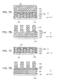
- FIGS. 11A to 11D are schematic cross-sectional views in order of the processes, illustrating a method for manufacturing a nonvolatile storage device of a comparative example
- FIGS. 12A to 12D are schematic cross-sectional views in order of the processes, continuing from FIG. 11D ;
- FIGS. 13A to 13D are schematic cross-sectional views in order of the processes, continuing from FIG. 12D ;
- FIG. 14 is a flow chart illustrating a method for manufacturing a nonvolatile storage device according to the second embodiment of the invention.
- FIGS. 15A and 15B are schematic views illustrating the configuration of a nonvolatile storage device manufactured by the method for manufacturing a nonvolatile storage device according to the second embodiment of the invention.
- FIGS. 16A to 16D are schematic cross-sectional views illustrating the configuration of the nonvolatile storage device manufactured by the method for manufacturing a nonvolatile storage device according to the second embodiment of the invention.
- FIGS. 17A to 17D are schematic cross-sectional views in order of the processes, illustrating a method for manufacturing a nonvolatile storage device according to the second embodiment of the invention.
- FIGS. 18A to 18D are schematic cross-sectional views in order of the processes, continuing from FIG. 17D ;
- FIG. 19 is a schematic perspective view illustrating the configuration of another nonvolatile storage device manufactured by the method for manufacturing a nonvolatile storage device according to the second embodiment of the invention.
- FIG. 20 is a flow chart illustrating a method for manufacturing a nonvolatile storage device according to a third embodiment of the invention.
- FIGS. 21A and 21B are schematic views illustrating the configuration of a nonvolatile storage device manufactured by the method for manufacturing a nonvolatile storage device according to the third embodiment of the invention.
- FIGS. 22A to 22D are schematic cross-sectional views illustrating the configuration of the nonvolatile storage device manufactured by the method for manufacturing a nonvolatile storage device according to the third embodiment of the invention.
- FIGS. 23A to 23D are schematic cross-sectional views in order of the processes, illustrating the method for manufacturing a nonvolatile storage device according to the third embodiment of the invention.
- FIGS. 24A to 24D are schematic cross-sectional views in order of the processes, continuing from FIG. 23D .
- FIGS. 25A to 25D are schematic cross-sectional views in order of the processes, continuing from FIG. 24D ;
- FIGS. 26A to 26D are schematic cross-sectional views in order of the processes, continuing from FIG. 25D ;
- FIGS. 27A to 27D are schematic cross-sectional views in order of the processes, continuing from FIG. 26D ;
- FIGS. 28A to 28D are schematic cross-sectional views in order of the processes, continuing from FIG. 27D ;
- FIGS. 29A to 29D are schematic cross-sectional views in order of the processes, continuing from FIG. 28D ;
- FIG. 30 is a schematic cross-sectional view illustrating a relevant part of the nonvolatile storage device in a process of the method for manufacturing a nonvolatile storage device according to the third embodiment of the invention.
- FIGS. 31A to 31D are schematic cross-sectional views in order of the processes, illustrating a method for manufacturing a nonvolatile storage device of a comparative example
- FIGS. 32A to 32D are schematic cross-sectional views in order of the processes, continuing from FIG. 31D ;
- FIGS. 33A to 33D are schematic cross-sectional views in order of the processes, continuing from FIG. 32D ;
- FIG. 34 is a flow chart illustrating a method for manufacturing a nonvolatile storage device according to a fourth embodiment of the invention.
- FIGS. 35A and 35B are schematic views illustrating the configuration of a nonvolatile storage device manufactured by the method for manufacturing a nonvolatile storage device according to the fourth embodiment of the invention.
- FIGS. 36A to 36D are schematic cross-sectional views illustrating the configuration of the nonvolatile storage device manufactured by the method for manufacturing a nonvolatile storage device according to the fourth embodiment of the invention.
- FIGS. 37A to 37D are schematic cross-sectional views in order of the processes, illustrating the method for manufacturing a nonvolatile storage device according to the fourth embodiment of the invention.
- FIGS. 38A to 38D are schematic cross-sectional views in order of the processes, continuing from FIG. 37D ;
- FIG. 39 is a schematic perspective view illustrating the configuration of another nonvolatile storage device manufactured by the method for manufacturing a nonvolatile storage device according to the fourth embodiment of the invention.
- FIGS. 40A and 40B are schematic cross-sectional views of relevant parts of a storage unit of a nonvolatile storage device according to a fifth embodiment of the invention.
- FIG. 41 is a schematic cross-sectional view of a relevant part of the storage unit of the nonvolatile storage device according to the fifth embodiment of the invention.
- FIGS. 42 to 50D are views of relevant parts of the manufacturing process for forming a memory cell according to the fifth embodiment of the invention.
- FIGS. 51A and 51B are schematic stereographs of a relevant part for describing a comparative example.
- FIG. 1 is a flow chart illustrating a method for manufacturing a nonvolatile storage device according to a first embodiment of the invention.
- FIGS. 2A and 2B are schematic views illustrating the configuration of a nonvolatile storage device manufactured by the method for manufacturing a nonvolatile storage device according to the first embodiment of the invention.
- FIG. 2A is a perspective view
- FIG. 2B is a plan view.
- FIGS. 3A to 3D are schematic cross-sectional views illustrating the configuration of the nonvolatile storage device manufactured by the method for manufacturing a nonvolatile storage device according to the first embodiment of the invention.
- FIG. 3A is a cross-sectional view taken along line A-A′ of FIG. 2B
- FIG. 3B is a cross-sectional view taken along line B-B′ of FIG. 2B
- FIG. 3C is a cross-sectional view taken along line C-C′ of FIG. 2B
- FIG. 3D is a cross-sectional view taken along line D-D′ of FIG. 2B .
- FIGS. 4A to 4D are schematic cross-sectional views in order of the processes, illustrating the method for manufacturing a nonvolatile storage device according to the first embodiment of the invention.
- FIGS. 5A to 5D are schematic cross-sectional views in order of the processes, continuing from FIG. 4D .
- FIGS. 6A to 6D are schematic cross-sectional views in order of the processes, continuing from FIG. 5D .
- FIGS. 7A to 7D are schematic cross-sectional views in order of the processes, continuing from FIG. 6D .
- FIGS. 8A to 8D are schematic cross-sectional views in order of the processes, continuing from FIG. 7D .
- FIGS. 9A to 9D are schematic cross-sectional views in order of the processes, continuing from FIG. 8D .
- FIGS. 10A to 10D are schematic cross-sectional views in order of the processes, continuing from FIG. 9D .
- each drawing of the number including “A” is a cross-sectional view corresponding to line A-A′ of FIG. 2B
- each drawing of the number including “B” is a cross-sectional view corresponding to line B-B′ of FIG. 2B
- each drawing of the number including “C” is a cross-sectional view corresponding to line C-C′ of FIG. 2B
- each drawing of the number including “D” is a cross-sectional view corresponding to line D-D′ of FIG. 2B .
- FIGS. 2A and 2B and FIGS. 3A to 3D a nonvolatile storage device manufactured by the method for manufacturing a nonvolatile storage device according to the first embodiment of the invention will now be described with reference to FIGS. 2A and 2B and FIGS. 3A to 3D .
- a nonvolatile storage device 10 manufactured by the method for manufacturing a nonvolatile storage device according to this embodiment includes: a plurality of first electrodes 110 aligning in a first direction; a plurality of second electrodes 140 aligning in a second direction nonparallel to the first direction and provided above the first electrodes 110 ; and a first storage unit 130 provided between the first electrode 110 and the second electrode 140 and including a first storage layer 132 of which the resistance changes by at least one of an applied electric field and an applied current.
- the first electrodes 110 are provided on a major surface 106 of a substrate 105 , for example.
- the first direction and the second direction are nonparallel to each other, and for example, intersect three-dimensionally.
- a description is given by taking up the case where the first direction and the second direction are orthogonal to each other.
- the first direction is defined as an X-axis direction
- the second direction is defined as a Y-axis direction orthogonal to the X-axis direction.
- the direction orthogonal to the X-axis direction and the Y-axis direction is defined as a Z-axis direction.
- the major surface 106 of the substrate 105 is perpendicular to the Z-axis direction and parallel to the X-Y plane.
- the first electrode 110 aligns in the X-axis direction in a strip shape in a plane parallel to the X-Y plane.
- the second electrode 140 aligns in the Y-axis direction in a strip shape in a plane parallel to the X-Y plane.
- the first storage unit 130 is provided between the first electrode 110 and the second electrode 140 , where the first electrode 110 and the second electrode 140 intersect three-dimensionally.
- the first storage unit 130 forms a first memory cell 135 . That is, the nonvolatile storage device 10 is a crosspoint nonvolatile storage device using a resistance change film.
- the first electrode 110 serves as a bit line
- the second electrode 140 serves as a word line, for example.
- the first electrode 110 and the second electrode 140 may be replaced with each other in the invention.
- the first electrode 110 may serve as a word line
- the second electrode 140 may serve as a bit line.
- the first storage unit 130 includes the first storage layer 132 .
- the first storage layer 132 is a layer of which the resistance changes by at least one of an applied electric field and an applied current.
- a resistance change material, a phase change material of which the resistance changes with phase change, and the like may be used for the first storage layer 132 .
- a material in which various conductive films and/or various barrier films are stacked on the layer of resistance change material or the layer of phase change material may be used for the first storage layer 132 .
- NiO x , TiO x , CoO x , TaO x , MnO x , WO x , Al 2 O 3 , FeO x , HfO x , ZnMn 2 O 4 , ZnFe 2 O 4 , ZnCO 2 O 4 , ZnCr 2 O 4 , ZnAl 2 O 4 , CuCoO 2 , CuAlO 2 , NiWO 4 , NiTiO 3 , CoAl 2 O 4 , MnAl 2 O 4 , ZnNiTiO 4 , Pr x Ca 1-x MnO 3 , and the like may be used for the first storage layer 132 .
- the first storage layer 132 may be used for the first storage layer 132 .
- the invention is not limited to the above, but any material may be used for the first storage layer 132 .
- the first storage unit 130 may further include a first rectifying element 131 such as a diode.
- a first rectifying element 131 such as a diode.
- the first rectifying element 131 is provided between the first electrode 110 and the first storage layer 132 in this specific example, the first rectifying element 131 may be provided between the second electrode 140 and the first storage layer 132 .
- Various kinds of elements having rectifying function such as a PIN diode and a Schottky diode may be used for the first rectifying element 131 .
- a material in which an element having rectifying function, various conductive films, and various barrier films are stacked may be used for the first rectifying element 131 .
- the first electrode 110 , the first storage unit 130 , and the second electrode 140 are stacked in the Z-axis direction in the nonvolatile storage device 10 , and the nonvolatile storage device 10 includes a layer of memory cell array (a first memory cell array 101 ).
- nonvolatile storage devices manufactured by the method for manufacturing a nonvolatile storage device according to the embodiment of the invention may have a configuration in which a plurality of memory cell arrays are stacked in the Z-axis direction. In the following, first, a description is given by taking up the case where the nonvolatile storage device 10 includes one layer of memory cell array, for the sake of simplicity.
- a first interlayer insulating film 180 made of silicon oxide or the like is buried around the first memory cell 135 formed between the first electrode 110 and the second electrode 140 .
- the first storage unit 130 (the first rectifying element 131 and the first storage layer 132 ) may become in a tapered shape at the time of the processing of the first storage unit 130 .
- the cross section of the first storage unit 130 when it is cut with a plane parallel to the X-Y plane may be large on the lower side (the substrate 105 side) and small on the upper side (the side opposite to the substrate 105 ).
- the method for manufacturing a nonvolatile storage device does not cause a processing failure even when the first storage unit 130 has a tapered shape.
- a first electrode film 110 f that forms the first electrodes 110 and a first storage unit film 130 f that forms the first storage units 130 are stacked on the major surface 106 of the substrate 105 .
- the first storage unit film 130 f is specifically a stacked film of a first rectifying element film 131 f that forms the first rectifying elements 131 and a first storage layer film 132 f that forms the first storage layers 132 .
- This process corresponds to step S 110 illustrated in FIG. 1 .
- the first electrode film 110 f and the first storage unit film 130 f are processed into strip shapes aligning in the first direction (e.g. the X-axis direction).
- the X-axis direction is assigned to the first direction.
- This process corresponds to step S 120 illustrated in FIG. 1 .
- the first electrode film 110 f and the first storage unit film 130 f are processed by, for example, RIE (reactive ion etching) using a mask (not illustrated) of a silicon oxide film that is processed into strip shapes in the first direction in which the first electrode 110 aligns by photolithography.
- RIE reactive ion etching
- the first storage unit film 130 f may be processed into tapered shapes.
- the width of the strip of the first storage unit film 130 f on the first electrode film 110 f side is longer than the width of the strip on the side opposite to the first electrode film 110 f (that is, the length in a direction perpendicular to the first direction).
- a sacrifice layer 181 is buried between the processed first electrode films 110 f and between the processed first storage unit films 130 f.
- This process corresponds to step S 130 illustrated in FIG. 1 .
- a novolac resin that is an organic film is used for the sacrifice layer 181 . That is, the novolac resin is applied on the first electrode film 110 f , the first storage unit film 130 f , and the substrate 105 ; the novolac resin is buried between the first electrode films 110 f and between the first storage unit films 130 f ; and the novolac resin is cured by heat treatment.
- etchback is performed by using, for example, plasma including ammonia and oxygen to decrease the film thickness of the novolac resin.
- a first cap layer 182 (a cap layer) made of, for example, silicon oxide is buried by plasma CVD (chemical vapor deposition) or the application method, and is planarized by CMP (chemical mechanical polishing).
- the sacrifice layer 181 is located lower than the interface planarized by CMP; a configuration in which the first cap layer 182 is stacked thereon can be formed; and unintended damage to the sacrifice layer 181 by subsequent processing is suppressed.
- the film thickness of the first cap layer 182 made of silicon oxide is preferably thin within the range that suppresses damage to the sacrifice layer 181 .
- the first cap layer 182 is provided as necessary and may be omitted.
- a second electrode film 140 f that forms the second electrodes 140 is formed above the first electrode film 110 f and on the first storage unit film 130 f and the sacrifice layer 181 (and the first cap layer).
- This process corresponds to step S 140 illustrated in FIG. 1 .
- a mask layer 150 formed into the shape of the second electrodes 140 by photolithography is formed.
- This process corresponds to step S 150 illustrated in FIG. 1 .
- the mask layer 150 has a lower etching rate than the sacrifice layer 181 .
- silicon oxide is used for the mask layer 150 .
- the second electrode film 140 f is processed into strip shapes aligning in the second direction by using the mask layer 150 as a mask.
- RIE for example, is used for this processing.
- This process corresponds to step S 160 illustrated in FIG. 1 .
- the first cap layer 182 made of silicon oxide is removed by dry etching or dilute hydrofluoric acid treatment using the mask layer 150 as a mask.
- the first cap layer 182 is provided as necessary. In the case where the first cap layer 182 is not formed, this process is omitted. Furthermore, in the case where the first cap layer 182 is thin, the process that removes the first cap layer 182 may not be provided in particular, and the first cap layer 182 may be removed at the time of other processing in the process described later.
- the columnar shape is a shape that includes a side wall along the first direction (the X-axis direction) and a side wall along the second direction (the Y-axis direction).
- This process corresponds to step S 170 illustrated in FIG. 1 .
- the first storage unit film 130 f since the first storage unit film 130 f has been processed into a strip shape having a side wall along the first direction (the X-axis direction) in step S 120 described above, the first storage unit film 130 f is processed so as to have a side wall along the second direction (the Y-axis direction) in step S 170 into columnar shapes.
- the first storage unit film 130 f has a tapered shape in the cross section taken along line C-C′ of FIG. 2B , and the first storage unit film 130 f is covered with the sacrifice layer 181 in this portion. Therefore, the portion where the first storage unit film 130 f is covered with the sacrifice layer 181 is left without being etched.
- the sacrifice layer 181 is removed to expose the first storage unit film 130 f that has been covered with the sacrifice layer 181 .
- This process corresponds to step S 171 illustrated in FIG. 1 .
- the sacrifice layer 181 can be removed by using plasma using oxygen gas or mixed gas of oxygen and ammonia, for example.
- the sacrifice layer 181 can be removed without damaging the mask layer 150 substantially.
- the mask layer 150 e.g. silicon oxide
- This process corresponds to step S 172 illustrated in FIG. 1 .
- the mask layer 150 is removed; the sacrifice layer 181 is removed by isotropic etching by plasma including oxygen, ammonia, hydrogen, water, and the like, for example; and then silicon oxide that forms the first interlayer insulating film 180 is buried between the first electrode films 110 f , between the first storage unit films 130 f , and between the second electrode films 140 f by a method such as CVD and SOG (spin on glass).
- a method such as CVD and SOG (spin on glass).
- the sacrifice layer 181 is removed after step S 172 and then the first interlayer insulating film 180 is formed in the above, the sacrifice layer 181 may not be removed after step S 172 , and the first interlayer insulating film 180 may be formed in the state in which the sacrifice layer 181 is left.
- FIGS. 11A to 11D are schematic cross-sectional views in order of the processes, illustrating a method for manufacturing a nonvolatile storage device of a comparative example.
- FIGS. 12A to 12D are schematic cross-sectional views in order of the processes, continuing from FIG. 11D .
- FIGS. 13A to 13D are schematic cross-sectional views in order of the processes, continuing from FIG. 12D .
- FIGS. 11A to 11D are views compared with FIGS. 7A to 7D according to this embodiment
- FIGS. 12A to 12D are views compared with FIGS. 8A to 8D according to this embodiment
- FIGS. 13A to 13D are views compared with FIGS. 9A to 9D according to this embodiment.
- the first electrode film 110 f and the first storage unit film 130 f are stacked on the substrate 105 (step S 110 ); the first electrode film 110 f and the first storage unit film 130 f are processed into strip shapes aligning in the first direction (step S 120 ); and then an interlayer insulating film 190 made of silicon oxide is buried between the first electrode films 110 f and between the first storage unit films 130 f.
- the second electrode film 140 f that forms the second electrodes 140 is formed (step S 140 ); the mask layer 150 is formed (step S 150 ); and the second electrode film 140 f is processed into strip shapes aligning in the second direction by using the mask layer 150 as a mask (step S 160 ). Silicon oxide is used also for the mask layer 150 as in the case of the interlayer insulating film 190 .
- the sacrifice layer 181 e.g. a novolac resin
- the mask layer 150 e.g. silicon oxide
- the interlayer insulating film 190 e.g. silicon oxide
- the portion of the first storage unit film 130 f exposed from the interlayer insulating film 190 is processed into columnar shapes (step S 171 ) as illustrated in FIGS. 12A to 12D ; and when it is attempted to remove the interlayer insulating film 190 , a selection ratio of etching cannot be ensured between the interlayer insulating film 190 and the mask layer 150 , and therefore the film thickness of the mask layer 150 becomes thin by the etching for removing the interlayer insulating film 190 , as illustrated in FIGS. 13A to 13D . Furthermore, the line width of the mask layer 150 becomes narrow.
- the film thickness of the mask layer 150 decreases significantly, leading to an insufficient film thickness for the mask for subsequent dry etching.
- the wiring portion of the first electrode film 110 f is etched, and this causes the problems of an increased wiring resistance and disconnection.
- the mask layer 150 is damaged in the process of removing the interlayer insulating film 190 .
- the interlayer insulating film 190 is removed incompletely if it is attempted to maintain the shape of the mask layer 150 to some extent.
- the first storage unit film 130 f covered with the remaining interlayer insulating film 190 is not removed but left in subsequent processes, and this causes a short between the second electrodes 140 , for example.
- the sacrifice layer 181 of a material having a relatively higher etching rate than the mask layer 150 is used. Thereby, damage to the mask layer 150 can be suppressed at the time of removing the sacrifice layer 181 , and the sacrifice layer 181 that covers the first storage unit film 130 f in the regions exposed from the mask layer 150 can be removed substantially completely.
- the sacrifice layer 181 can be removed completely to expose the first storage unit film 130 f , and the first storage unit film 130 f remaining under the shade of the sacrifice layer 181 can be removed. Furthermore, the problem of the wiring resistance and the disconnection of the first electrode film 110 f particularly in the wiring portion also can be avoided.
- the method for manufacturing a nonvolatile storage device provides a method for manufacturing a nonvolatile storage device that reduces the processing failure of the storage unit between wirings and achieves a high yield.
- the mask layer 150 has a lower etching rate than the sacrifice layer 181 .
- the sacrifice layer 181 at least one selected from a group consisting of silicon oxide, silicon nitride, silicon oxynitride, and silicon carbide may be used for the mask layer 150 .
- the sacrifice layer 181 In the case where an application solution is used as the sacrifice layer 181 , a solution with a low surface tension and a high wettability is preferably used. Thereby, the sacrifice layer 181 can be applied between the processed first electrode films 110 f and between the processed first storage unit films 130 f with good wettability, and the generation of a void and the like can be suppressed.
- silicon oxide is used for the sacrifice layer 181
- at least one of silicon nitride and silicon carbide may be used for the mask layer 150 .
- the first cap layer 182 (for example, a film made of silicon oxide) having a lower etching rate than the sacrifice layer 181 may be buried between the processed first electrode films 110 f and between the processed first storage unit films 130 f . Thereby, damage to the sacrifice layer 181 can be suppressed.
- processing that uses plasma including gas including at least one selected from a group consisting of O 2 , H 2 , H 2 O, NH 3 , and CH 4 may be employed for the process of removing the sacrifice layer 181 in step S 171 .
- the sacrifice layer 181 made of an organic material can be etched, the amount of the recession of the mask layer 150 can be made small, and the margin of the processing process can be increased, without requiring large ion energy.
- Isotropic etching using downflow plasma using microwave, for example, or anisotropic etching using RIE, for example, may be used for removing the sacrifice layer 181 in step S 171 .
- the sacrifice layer 181 located below the second electrode 140 also is etched.
- the sacrifice layer 181 located below the second electrode 140 is not completely removed.
- a protection film such as a silicon oxide film and a silicon nitride film may be formed on the side walls of the first electrode film 110 f , the second electrode film 140 f , and the first storage unit film 130 f by the ALD (atomic layer deposition) method and the like. Thereby, the oxidation and reaction of the side walls can be suppressed.
- ALD atomic layer deposition
- a method for manufacturing a nonvolatile storage device according to a second embodiment of the invention is used for a nonvolatile storage device in which a plurality of memory cell arrays are stacked.
- FIG. 14 is a flow chart illustrating a method for manufacturing a nonvolatile storage device according to the second embodiment of the invention.
- FIGS. 15A and 15B are schematic views illustrating the configuration of a nonvolatile storage device manufactured by the method for manufacturing a nonvolatile storage device according to the second embodiment of the invention.
- FIG. 15A is a perspective view
- FIG. 15B is a plan view.
- FIGS. 16A to 16D are schematic cross-sectional views illustrating the configuration of the nonvolatile storage device manufactured by the method for manufacturing a nonvolatile storage device according to the second embodiment of the invention.
- FIG. 16A is a cross-sectional view taken along line A-A′ of FIG. 15B
- FIG. 16B is a cross-sectional view taken along line B-B′ of FIG. 15B
- FIG. 16C is a cross-sectional view taken along line C-C′ of FIG. 15B
- FIG. 16D is a cross-sectional view taken along line D-D′ of FIG. 15B .
- FIGS. 17A to 17D are schematic cross-sectional views in order of the processes, illustrating a method for manufacturing a nonvolatile storage device according to the second embodiment of the invention.
- FIGS. 18A to 18D are schematic cross-sectional views in order of the processes, continuing from FIG. 17D .
- a nonvolatile storage device 20 manufactured by the manufacturing method according to the second embodiment includes a plurality of memory cell arrays stacked in the Z-axis direction.
- the first memory cell array 101 may be similar to that described in regard to the first embodiment, and a description is therefore omitted.
- a second memory cell array 201 is stacked on the first memory cell array 101 in the Z-axis direction.
- the second memory cell array 201 includes the second electrodes 140 , third electrodes 240 , and a second storage unit 230 provided between the second electrode 140 and the third electrode 240 .
- the second electrode 140 in the second memory cell array 201 functions also as the second electrode 140 in the first memory cell array 101 .
- the second electrode 140 is a word line, for example, and the third electrode 240 is a bit line, for example.
- the second storage unit 230 includes a second storage layer 232 .
- the second storage layer 232 is a layer of which the resistance changes by at least one of an applied electric field and an applied current.
- the second storage unit 230 may further include a second rectifying element 231 .
- the second rectifying element 231 is provided between the second electrode 140 and the second storage layer 232 in this specific example, the second rectifying element 231 may be provided between the third electrode 240 and the second storage layer 232 , and the stacking order is arbitrary.
- the configuration and material described in regard to the first storage unit 130 , the first storage layer 132 , the first rectifying element 131 , and the first electrode 110 (or the second electrode 140 ) may be used for the second storage unit 230 , the second storage layer 232 , the second rectifying element 231 , and the third electrode 240 . Therefore, a description is omitted.
- a second interlayer insulating film 280 made of silicon oxide or the like is buried around a second memory cell 235 formed between the second electrode 140 and the third electrode 240 .
- a method for manufacturing the nonvolatile storage device 20 having such a configuration will now be described with reference to FIG. 14 and FIG. 17A to FIG. 18D .
- the first electrode film 110 f that forms the first electrodes 110 and the first storage unit film 130 f that forms the first storage units 130 are stacked on the major surface 106 of the substrate 105 (step S 210 illustrated in FIG. 14 ). Then, the first electrode film 110 f and the first storage unit film 130 f are processed into strip shapes aligning in the first direction (step S 220 ). At this time, the first storage unit film 130 f may be processed into tapered shapes.
- the sacrifice layer 181 is buried between the processed first electrode films 110 f and between the processed first storage unit films 130 f (step S 230 ).
- a novolac resin for example, is used as the sacrifice layer 181 .
- the second storage unit film 230 f includes a second rectifying element film 231 f that forms the second rectifying elements 231 and a second storage layer film 232 f that forms the second storage layers 232 , for example.
- the mask layer 150 having a lower etching rate than the sacrifice layer 181 is formed on the second storage unit film 230 f (step S 250 ).
- Silicon oxide for example, is used as the mask layer 150 .
- the second electrode film 140 f and the second storage unit film 230 f are processed into strip shapes aligning in the second direction by using the mask layer 150 as a mask (step S 260 ).
- the portion of the first storage unit film 130 f exposed from the sacrifice layer 181 is processed into columnar shapes including a side wall along the first direction and a side wall along the second direction by using the mask layer 150 as a mask (step S 270 ).
- the first storage unit film 130 f has a tapered shape in the cross section taken along line C-C′ of FIG. 15B , and the first storage unit film 130 f is covered with the sacrifice layer 181 in this portion. Therefore, the portion where the first storage unit film 130 f is covered with the sacrifice layer 181 is left without being etched.
- the sacrifice layer 181 is removed to expose the first storage unit film 130 f that has been covered with the sacrifice layer 181 (step S 271 ).
- the sacrifice layer 181 can be removed by using plasma using oxygen gas or mixed gas of oxygen and ammonia, for example.
- the sacrifice layer 181 can be removed without damaging the mask layer 150 substantially.
- the mask layer 150 e.g. silicon oxide
- step S 272 the exposed first storage unit film 130 f is removed.
- the mask layer 150 is removed, and the sacrifice layer 181 is removed by isotropic etching by plasma including oxygen, ammonia, hydrogen, water, and the like, for example.
- silicon oxide that forms the first interlayer insulating film 180 is buried between the first electrode films 110 f , between the first storage unit films 130 f , and between the second electrode films 140 f by a method such as CVD and SOG, for example.
- the memory cell array 101 of the first layer can be formed.
- the first interlayer insulating film 180 is provided at depths from the substrate 105 to the second electrode 140 , for example; a sacrifice layer of the second layer made of, for example, a novolac resin is formed on the upper side thereof; then a third electrode film that forms the third electrodes 240 is formed on the second storage unit film 230 f and the sacrifice layer of the second layer; the third electrode film is processed and the second storage unit film 230 f is processed into columnar shapes in the same manner as the memory cell array 101 of the first layer; and then the second interlayer insulating film 280 is buried.
- the nonvolatile storage device 20 illustrated in FIGS. 15A and 15B and FIGS. 16A to 16D can be manufactured.
- the manufacturing method according to this embodiment can manufacture the nonvolatile storage device 20 in which two memory cell arrays are stacked and the second electrode 140 is shared between the first layer and the second layer, and can reduce the processing failure of the storage unit between wirings and increase the yield also in this case.
- the method for manufacturing a nonvolatile storage device according to this embodiment can be used for a nonvolatile storage device in which any numbers of memory cell arrays are stacked.
- FIG. 19 is a schematic perspective view illustrating the configuration of another nonvolatile storage device manufactured by the method for manufacturing a nonvolatile storage device according to the second embodiment of the invention.
- the nonvolatile storage device 21 includes a first to a fourth memory cell array 101 , 201 , 301 , and 401 .
- the configuration of each of the memory cell arrays is similar to the nonvolatile storage devices 10 and 20 .
- the third memory cell array 301 includes the third electrodes 240 , fourth electrodes 340 , and a third storage unit 330 provided between the third electrode 240 and the fourth electrode 340 .
- the third storage unit 330 includes a third storage layer 332 and a third rectifying element layer 331 .
- the fourth memory cell array 401 includes the fourth electrodes 340 , fifth electrodes 440 , and a fourth storage unit 430 provided between the fourth electrode 340 and the fifth electrode 440 .
- the fourth storage unit 430 includes a fourth storage layer 432 and a fourth rectifying element layer 431 .
- the third electrode 240 is shared between the second memory cell array 201 and the third memory cell array 301 .
- the fourth electrode 340 is shared between the third memory cell array 301 and the fourth memory cell array 401 .
- the nonvolatile storage device that includes three or more memory cell arrays and shares the electrode between mutually stacked memory cell arrays also can be manufactured by applying the method for manufacturing a nonvolatile storage device according to the second embodiment.
- nonvolatile storage device in which memory cell arrays are stacked and the electrode is not shared between mutually stacked memory cell arrays, it can be manufactured by applying the method for manufacturing a nonvolatile storage device according to the first embodiment.
- FIG. 20 is a flow chart illustrating a method for manufacturing a nonvolatile storage device according to a third embodiment of the invention.
- FIGS. 21A and 21B are schematic views illustrating the configuration of a nonvolatile storage device manufactured by the method for manufacturing a nonvolatile storage device according to the third embodiment of the invention.
- FIG. 21A is a perspective view
- FIG. 21B is a plan view.
- FIGS. 22A to 22D are schematic cross-sectional views illustrating the configuration of the nonvolatile storage device manufactured by the method for manufacturing a nonvolatile storage device according to the third embodiment of the invention.
- FIG. 22A is a cross-sectional view taken along line A-A′ of FIG. 21B
- FIG. 22B is a cross-sectional view taken along line B-B′ of FIG. 21B
- FIG. 22C is a cross-sectional view taken along line C-C of FIG. 21B
- FIG. 22D is a cross-sectional view taken along line D-D′ of FIG. 21B .
- FIGS. 23A to 23D are schematic cross-sectional views in order of the processes, illustrating the method for manufacturing a nonvolatile storage device according to the third embodiment of the invention.
- FIGS. 24A to 24D are schematic cross-sectional views in order of the processes, continuing from FIG. 23D .
- FIGS. 25A to 25D are schematic cross-sectional views in order of the processes, continuing from FIG. 24D .
- FIGS. 26A to 26D are schematic cross-sectional views in order of the processes, continuing from FIG. 25D .
- FIGS. 27A to 27D are schematic cross-sectional views in order of the processes, continuing from FIG. 26D .
- FIGS. 28A to 28D are schematic cross-sectional views in order of the processes, continuing from FIG. 27D .
- FIGS. 29A to 29D are schematic cross-sectional views in order of the processes, continuing from FIG. 28D .
- FIG. 30 is a schematic cross-sectional view illustrating a relevant part of the nonvolatile storage device in a process of the method for manufacturing a nonvolatile storage device according to the third embodiment of the invention.
- each drawing of the number including “A” is a cross-sectional view corresponding to line A-A′ of FIG. 21B
- each drawing of the number including “B” is a cross-sectional view corresponding to line B-B′ of FIG. 21B
- each drawing of the number including “C” is a cross-sectional view corresponding to line C-C′ of FIG. 21B
- each drawing of the number including “D” is a cross-sectional view corresponding to line D-D′ of FIG. 21B .
- FIGS. 21A and 21B and FIGS. 22A to 22D a nonvolatile storage device manufactured by the method for manufacturing a nonvolatile storage device according to the third embodiment of the invention will now be described with reference to FIGS. 21A and 21B and FIGS. 22A to 22D .
- a nonvolatile storage device 50 manufactured by the method for manufacturing a nonvolatile storage device according to this embodiment includes: the plurality of first electrodes 110 aligning in the first direction; the plurality of second electrodes 140 aligning in the second direction nonparallel to the first direction and provided above the first electrodes 110 ; and the plurality of first storage units 130 each provided between each of the plurality of first electrodes 110 and each of the plurality of second electrodes 140 and each including a first storage layer 132 of which the resistance changes by at least one of an applied electric field and an applied current.
- the first electrodes 110 are provided on the major surface 106 of the substrate 105 , for example.
- the first direction and the second direction are nonparallel to each other, and for example, intersect three-dimensionally.
- a description is given by taking up the case where the first direction and the second direction are orthogonal to each other.
- the first direction is defined as the X-axis direction
- the second direction is defined as the Y-axis direction orthogonal to the X-axis direction.
- the direction orthogonal to the X-axis direction and the Y-axis direction is defined as the Z-axis direction.
- the major surface 106 of the substrate 105 is perpendicular to the Z-axis direction and parallel to the X-Y plane.
- the first electrode 110 aligns in the X-axis direction in a strip shape in a plane parallel to the X-Y plane.
- the second electrode 140 aligns in the Y-axis direction in a strip shape in a plane parallel to the X-Y plane.
- the first electrode 110 and the second electrode 140 intersect three-dimensionally.
- the first storage unit 130 is provided between the first electrode 110 and the second electrode 140 to form the first memory cell 135 . That is, the nonvolatile storage device 50 is a crosspoint nonvolatile storage device using a resistance change film.
- the first electrode 110 serves as a bit line
- the second electrode 140 serves as a word line, for example.
- the first electrode 110 and the second electrode 140 may be replaced with each other, and the first electrode 110 may serve as a word line and the second electrode 140 may serve as a bit line.
- the first storage unit 130 includes the first storage layer 132 .
- the first storage layer 132 is a layer of which the resistance changes by at least one of an applied electric field and an applied current.
- a resistance change material, a phase change material of which the resistance changes with phase change, and the like may be used for the first storage layer 132 .
- a material in which various conductive films and/or various barrier films are stacked may be used for the layer of resistance change material or the layer of phase change material of the first storage layer 132 .
- NiO x , TiO x , CoO x , TaO x , MnO x , WO x , Al 2 O 3 , FeO x , HfO x , ZnMn 2 O 4 , ZnFe 2 O 4 , ZnCO 2 O 4 , ZnCr 2 O 4 , ZnAl 2 O 4 , CuCoO 2 , CuAlO 2 , NiWO 4 , NiTiO 3 , CoAl 2 O 4 , MnAl 2 O 4 , ZnNiTiO 4 , Pr x Ca 1-x MnO 3 , and the like may be used for the first storage layer 132 .
- the first storage layer 132 may be used for the first storage layer 132 .
- the invention is not limited to the above, but any material may be used for the first storage layer 132 .
- the first storage unit 130 may further include the first rectifying element 131 such as a diode.
- the first rectifying element 131 is provided between the first electrode 110 and the first storage layer 132 in this specific example, the first rectifying element 131 may be provided between the second electrode 140 and the first storage layer 132 .
- Various kinds of elements having rectifying function such as a PIN diode and a Schottky diode may be used for the first rectifying element 131 .
- a material in which an element having rectifying function, various conductive films, and various barrier films are stacked may be used for the first rectifying element 131 .
- the first electrode 110 , the first storage unit 130 , and the second electrode 140 are stacked in the Z-axis direction in the nonvolatile storage device 50 , and the nonvolatile storage device 50 includes a layer of memory cell array (the first memory cell array 101 ).
- nonvolatile storage devices manufactured by the method for manufacturing a nonvolatile storage device according to the embodiment of the invention may have a configuration in which a plurality of memory cell arrays are stacked in the Z-axis direction. In the following, first, a description is given by taking up the case where the nonvolatile storage device 50 includes one layer of memory cell array, for the sake of simplicity.
- an interlayer insulating film 580 (an insulating film) is buried around the first memory cell 135 formed between the first electrode 110 and the second electrode 140 .
- the interlayer insulating film 580 includes a void 585 as described later. That is, the nonvolatile storage device 50 includes the interlayer insulating film 580 provided in at least one of between one pair of the plurality of first electrodes 110 , between one pair of the plurality of second electrodes 140 , and between one pair of the plurality of first storage units 130 and including the void 585 .
- the interlayer insulating film 580 including the void 585 may be provided between the substrate 105 and one of the plurality of second electrodes 140 .
- Silicon oxide for example, may be used for the interlayer insulating film 580 .
- the first storage unit 130 may become in a tapered shape at the time of the processing of the first storage unit 130 (the first rectifying element 131 and the first storage layer 132 ).
- the cross section of the first storage unit 130 when it is cut with a plane parallel to the X-Y plane may be large on the lower side (the substrate 105 side) and small on the upper side (the side opposite to the substrate 105 ).
- the method for manufacturing a nonvolatile storage device does not cause a processing failure even when the first storage unit 130 has a tapered shape.
- the first electrode film 110 f that forms the first electrodes 110 and the first storage unit film 130 f that forms the first storage units 130 are stacked on the major surface 106 of the substrate 105 .
- the first storage unit film 130 f is specifically a stacked film of the first rectifying element film 131 f that forms the first rectifying elements 131 and the first storage layer film 132 f that forms the first storage layers 132 .
- This process corresponds to step S 510 illustrated in FIG. 20 .
- the first electrode film 110 f and the first storage unit film 130 f are processed into strip shapes aligning in the first direction (e.g. the X-axis direction).
- the X-axis direction is assigned to the first direction.
- This process corresponds to step S 520 illustrated in FIG. 20 .
- the first electrode film 110 f and the first storage unit film 130 f are processed by, for example, RIE (reactive ion etching) using a mask (not illustrated) of a silicon oxide film that is processed into strip shapes in the first direction in which the first electrode 110 aligns by photolithography.
- RIE reactive ion etching
- the first storage unit film 130 f may be processed into tapered shapes.
- the width of the strip of the first storage unit film 130 f on the first electrode film 110 f side (that is, the length in a direction perpendicular to the first direction) becomes longer than the width of the strip on the side opposite to the first electrode film 110 f (that is, the length in a direction perpendicular to the first direction).
- a layer of a prescribed density 581 is buried between the processed first electrode films 110 f and between the processed first storage unit films 130 f.
- This process corresponds to step S 530 illustrated in FIG. 20 .
- the layer of a prescribed density 581 includes the void 585 , for example.
- the layer of a prescribed density 581 is formed by the following method, for example. Hydrophilization processing that hydrophilizes at least the side walls of the processed first electrode film 110 f and the processed first storage unit film 130 f is performed; a hydrophobic layer solution of a prescribed density that forms the layer of a prescribed density 581 is applied between the first electrode films 110 f and between the first storage unit films 130 f ; and heating is performed. Thereby, the layer of a prescribed density 581 is buried between the first electrode films 110 f and between the first storage unit films 130 f.
- a liner film (a thin film) made of, for example, SiO x is formed by, for example, ALD (atomic layer deposition) on the side walls and upper surfaces of the processed first electrode film 110 f and the processed first storage unit film 130 f , and then the hydrophilization processing that hydrophilizes the surface of the liner film is performed.
- ALD atomic layer deposition
- At least one of treatment with a mixed solution of choline and hydrogen peroxide solution and hot water treatment may be used for the hydrophization processing.
- An aqueous solution containing 1 to 10% choline and 1 to 10% hydrogen peroxide solution, for example, may be used as the mixed solution of choline and hydrogen peroxide solution.
- Hot water of approximately 70° C. to 85° C., for example, may be used for the hot water treatment.
- a layer solution of a prescribed density that forms the layer of a prescribed density 581 is applied between the first electrode films 110 f and between the first storage unit films 130 f , where at least the side walls of the first electrode film 110 f and the first storage unit film 130 f have been hydrophilized.
- a solution of hydrophobic polysilazane may be used as the layer solution of a prescribed density.
- the polysilazane is heated to 400° C. or higher, for example, to generate silicon oxide. This silicon oxide forms the layer of a prescribed density 581 .
- the void 585 is formed in the layer of a prescribed density 581 .
- the void 585 is formed by the following, for example. That is, the hydrophobic layer solution of a prescribed density is applied on the side walls of the first electrode film 110 f and the first storage unit film 130 f on which the hydrophilization processing has been performed, and the workpiece is heated in this state to be calcined; and consequently the void 585 is formed possibly by the interaction between the hydrophilized surface and the hydrophobic layer solution of a prescribed density at the interface of both.
- the void 585 for example, is generated in the layer of a prescribed density 581 . Therefore, the formation of the liner film and the hydrophilization processing mentioned above are performed as necessary, and may be omitted.
- the second electrode film 140 f that forms the second electrodes 140 is formed above the first electrode film 110 f and on the first storage unit film 130 f and the layer of a prescribed density 581 .
- This process corresponds to step S 540 illustrated in FIG. 20 .
- the mask layer 150 processed into the shape of the second electrodes 140 by photolithography is formed.
- This process corresponds to step S 550 illustrated in FIG. 20 .
- a film having a higher density than the layer of a prescribed density 581 is used for the mask layer 150 . That is, in the case where, for example, a silicon oxide film including the void 585 is used as the layer of a prescribed density 581 , a silicon oxide film, for example, that is dense and includes no void is used for the mask layer 150 .
- the second electrode film 140 f is processed into strip shapes aligning in the second direction by using the mask layer 150 as a mask.
- RIE for example, is used for this processing.
- This process corresponds to step S 560 illustrated in FIG. 20 .
- the columnar shape is a shape that includes a side wall along the first direction (the X-axis direction) and a side wall along the second direction (the Y-axis direction).
- This process corresponds to step S 570 illustrated in FIG. 20 .
- the first storage unit film 130 f since the first storage unit film 130 f has been processed into a strip shape that includes a side wall along the first direction (the X-axis direction) in step S 520 described above, the first storage unit film 130 f is processed so as to include a side wall along the second direction (the Y-axis direction) in step S 570 into columnar shapes.
- the first storage unit film 130 f has a tapered shape in the cross section taken along line C-C′ of FIG. 21B , and the first storage unit film 130 f is covered with the layer of a prescribed density 581 in this portion. Therefore, the portion where the first storage unit film 130 f is covered with the layer of a prescribed density 581 is left without being etched.
- the layer of a prescribed density 581 is removed to expose the first storage unit film 130 f that has been covered with the layer of a prescribed density 581 .
- This process corresponds to step S 571 illustrated in FIG. 20 .
- the layer of a prescribed density 581 can be removed by treatment with dilute hydrofluoric acid.
- the layer of a prescribed density 581 can be removed by using hydrofluoric acid of 3%, for example, as the dilute hydrofluoric acid and performing treatment of approximately 120 seconds, for example.
- the layer of a prescribed density 581 can be removed without damaging the mask layer 150 substantially.
- This process corresponds to step S 572 illustrated in FIG. 20 .
- the mask layer 150 is removed, and then silicon oxide that forms at least part of the interlayer insulating film 580 is buried between the first electrode films 110 f , between the first storage unit films 130 f , and between the second electrode films 140 f by a method such as CVD and SOG (spin on glass).
- CVD and SOG spin on glass
- step S 571 it is sufficient that the portion of the layer of a prescribed density 581 covering the first storage unit film 130 f having a tapered shape is removed, and it is not necessary to remove the entire layer of a prescribed density 581 . Accordingly, the layer of a prescribed density 581 may be left in the portion on the lower side (the substrate 105 side) of the second electrode film 140 f , for example.
- the interlayer insulating film 580 includes the layer of a prescribed density 581 . That is, the interlayer insulating film 580 includes the void 585 .
- FIGS. 31A to 31D are schematic cross-sectional views in order of the processes, illustrating a method for manufacturing a nonvolatile storage device of a comparative example.
- FIGS. 32A to 32D are schematic cross-sectional views in order of the processes, continuing from FIG. 31D .
- FIGS. 33A to 33D are schematic cross-sectional views in order of the processes, continuing from FIG. 32D .
- FIGS. 31A to 31D are drawings compared with FIGS. 26A to 26D according to this embodiment
- FIGS. 32A to 32D are drawings compared with FIGS. 27A to 27D according to this embodiment
- FIGS. 33A to 33D are drawings compared with FIGS. 28A to 28D according to this embodiment.
- the first electrode film 110 f and the first storage unit film 130 f are stacked on the substrate 105 (step S 510 ); the first electrode film 110 f and the first storage unit film 130 f are processed into strip shapes aligning in the first direction (step S 520 ); and then the interlayer insulating film 190 made of silicon oxide is buried between the first electrode films 110 f and between the first storage unit films 130 f.
- the second electrode film 140 f that forms the second electrodes 140 is formed (step S 540 ), the mask layer 150 is formed (step S 550 ), and the second electrode film 140 f is processed into strip shapes aligning in the second direction by using the mask layer 150 as a mask (step S 560 ). Silicon oxide is used also for the mask layer 150 as in the case of the interlayer insulating film 190 .
- step S 530 in the manufacturing method according to this embodiment the layer of a prescribed density 581 (for example, silicon oxide including the void 585 ) having a lower density than the mask layer 150 (for example, silicon oxide) is buried between the first electrode films 110 f and between the first storage unit films 130 f ; but in the case of the manufacturing method of the comparative example, the interlayer insulating film 190 (for example, silicon oxide) having the same density as the mask layer 150 is used.
- a prescribed density 581 for example, silicon oxide including the void 585
- the interlayer insulating film 190 for example, silicon oxide
- the portion of the first storage unit film 130 f exposed from the interlayer insulating film 190 is processed into columnar shapes as illustrated in FIGS. 32A to 32D (step S 571 ); and when it is attempted to remove the interlayer insulating film 190 , a selection ratio of etching cannot be ensured between the interlayer insulating film 190 and the mask layer 150 , and therefore the film thickness of the mask layer 150 becomes thin by the etching for removing the interlayer insulating film 190 , as illustrated in FIGS. 33A to 33D . Furthermore, the line width of the mask layer 150 becomes narrow.
- the film thickness of the mask layer 150 decreases significantly, leading to an insufficient film thickness for the mask for subsequent dry etching.
- the mask layer 150 is damaged in the process of removing the interlayer insulating film 190 .
- the interlayer insulating film 190 is removed insufficiently if it is attempted to maintain the shape of the mask layer 150 to some extent.
- the first storage unit film 130 f covered with the remaining interlayer insulating film 190 is not removed but left in subsequent processes, and this causes a short between the second electrodes 140 , for example.
- the layer of a prescribed density 581 having a lower density than the mask layer 150 damage to the mask layer 150 can be suppressed at the time of removing the layer of a prescribed density 581 , and the layer of a prescribed density 581 that covers the first storage unit film 130 f in the regions exposed from the mask layer 150 can be removed substantially completely.
- the layer of a prescribed density 581 can be removed completely to expose the first storage unit film 130 f , and the first storage unit film 130 f remaining under the shade of the layer of a prescribed density 581 can be removed.
- the method for manufacturing a nonvolatile storage device provides a method for manufacturing a nonvolatile storage device that reduces the processing failure of the storage unit between wirings and achieves a high yield.
- the mask layer 150 has a higher density than the layer of a prescribed density 581 .
- silicon oxide including the void 585 is used for the layer of a prescribed density 581
- at least one selected from a group consisting of dense silicon oxide, silicon nitride, silicon oxynitride, and silicon carbide that include no void may be used for the mask layer 150 .
- the nonvolatile storage device 50 manufactured in this embodiment includes the interlayer insulating film 580 provided at least one of between a pair of the plurality of first electrodes 110 , between a pair of the plurality of second electrodes 140 , and between a pair of the plurality of first storage units 130 and including the void 585 ; thereby, a nonvolatile storage device that reduces the processing failure of the storage unit between wirings and achieves a high yield can be provided.
- a method for manufacturing a nonvolatile storage device according to a fourth embodiment of the invention is used for a nonvolatile storage device in which a plurality of memory cell arrays are stacked.
- FIG. 34 is a flow chart illustrating a method for manufacturing a nonvolatile storage device according to the fourth embodiment of the invention.
- FIGS. 35A and 35B are schematic views illustrating the configuration of a nonvolatile storage device manufactured by the method for manufacturing a nonvolatile storage device according to the fourth embodiment of the invention.
- FIG. 35A is a perspective view
- FIG. 35B is a plan view.
- FIGS. 36A to 36D are schematic cross-sectional views illustrating the configuration of the nonvolatile storage device manufactured by the method for manufacturing a nonvolatile storage device according to the fourth embodiment of the invention.
- FIG. 36A is a cross-sectional view taken along line A-A′ of FIG. 35B
- FIG. 36B is a cross-sectional view taken along line B-B′ of FIG. 35B
- FIG. 36C is a cross-sectional view taken along line C-C′ of FIG. 35B
- FIG. 36D is a cross-sectional view taken along line D-D′ of FIG. 35B .
- FIGS. 37A to 37D are schematic cross-sectional views in order of the processes, illustrating the method for manufacturing a nonvolatile storage device according to the fourth embodiment of the invention.
- FIGS. 38A to 38D are schematic cross-sectional views in order of the processes, continuing from FIG. 37D .
- a plurality of memory cell arrays are provided to be stacked in the Z-axis direction in a nonvolatile storage device 60 manufactured by the manufacturing method according to the fourth embodiment.
- the first memory cell array 101 may be similar to that described in regard to the first embodiment, and a description is therefore omitted.
- the second memory cell array 201 is stacked on the first memory cell array 101 in the Z-axis direction.
- the second memory cell array 201 includes the second electrode 140 , the third electrode 240 , and the second storage unit 230 provided between the second electrode 140 and the third electrode 240 .
- the second electrode 140 in the second memory cell array 201 functions also as the second electrode 140 in the first memory cell array 101 .
- the second electrode 140 is a word line, for example, and the third electrode 240 is a bit line, for example.
- the second storage unit 230 includes the second storage layer 232 .
- the second storage layer 232 is a layer of which the resistance changes by at least one of an applied electric field and an applied current.
- the second storage unit 230 may further include the second rectifying element 231 .
- the second rectifying element 231 is provided between the second electrode 140 and the second storage layer 232 in this specific example, the second rectifying element 231 may be provided between the third electrode 240 and the second storage layer 232 , and the stacking order is arbitrary.
- the configuration and material described in regard to the first storage unit 130 , the first storage layer 132 , the first rectifying element 131 , and the first electrode 110 (or the second electrode 140 ) may be used for the second storage unit 230 , the second storage layer 232 , the second rectifying element 231 , and the third electrode 240 , and a description is therefore omitted.
- an interlayer insulating film of the second layer 680 (an insulating film) made of silicon oxide or the like is buried around the second memory cell 235 formed between the second electrode 140 and the third electrode 240 .
- the interlayer insulating film of the second layer 680 also may include a void 685 . That is, the nonvolatile storage device 60 may be provided at least one of between a pair of the plurality of second electrodes 140 , between a pair of the plurality of third electrodes 240 , and between a pair of the plurality of second storage units 230 , and may include the interlayer insulating film of the second layer 680 including the void 685 . Silicon oxide, for example, may be used for the interlayer insulating film of the second layer 680 . However, in the nonvolatile storage device 60 , at least one of the interlayer insulating film of the first layer 580 and the interlayer insulating film of the second layer 680 may include the void.
- the first electrode film 110 f that forms the first electrodes 110 and the first storage unit film 130 f that forms the first storage units 130 are stacked on the major surface 106 of the substrate 105 (step S 610 illustrated in FIG. 34 ). Then, the first electrode film 110 f and the first storage unit film 130 f are processed into strip shapes aligning in the first direction (step S 620 ). At this time, the first storage unit film 130 f may be processed into tapered shapes.
- the layer of a prescribed density 581 is buried between the processed first electrode films 110 f and between the processed first storage unit films 130 f (step S 630 ).
- Silicon oxide formed from polysilazane and including the void 585 for example, is used as the layer of a prescribed density 581 .
- the second storage unit film 230 f includes the second rectifying element film 231 f that forms the second rectifying elements 231 and the second storage layer film 232 f that forms the second storage layers 232 , for example.
- the mask layer 150 having a higher density than the layer of a prescribed density 581 is formed on the second storage unit film 230 f (step S 650 ).
- Dense silicon oxide including no void, for example, is used as the mask layer 150 .
- the second electrode film 140 f and the second storage unit film 230 f are processed into strip shapes aligning in the second direction by using the mask layer 150 as a mask (step S 660 ).
- the portion of the first storage unit film 130 f exposed from the layer of a prescribed density 581 is processed into columnar shapes including a side wall along the first direction and a side wall along the second direction by using the mask layer 150 as a mask (step S 670 ).
- the first storage unit film 130 f has a tapered shape in the cross section taken along line C-C′ of FIG. 35B , and the first storage unit film 130 f is covered with the layer of a prescribed density 581 in this portion. Therefore, the portion where the first storage unit film 130 f is covered with the layer of a prescribed density 581 is left without being etched.
- the layer of a prescribed density 581 is removed to expose the first storage unit film 130 f that has been covered with the layer of a prescribed density 581 (step S 671 ).
- the layer of a prescribed density 581 can be removed by treatment with dilute hydrofluoric acid, for example.
- silicon oxide including the void 585 for example, which has a lower density than the mask layer 150 (e.g. silicon oxide) is used as the layer of a prescribed density 581 , the layer of a prescribed density 581 can be removed without damaging the mask layer 150 substantially.
- step S 672 the exposed first storage unit film 130 f is removed.
- the mask layer 150 is removed, and silicon oxide that forms the interlayer insulating film of the first layer 580 is buried between the first electrode films 110 f , between the first storage unit films 130 f , and between the second electrode films 140 f by a method such as CVD and SOG.
- the memory cell array 101 of the first layer can be formed.
- the interlayer insulating film of the first layer 580 is provided at depths from the substrate 105 to the second electrode 140 , for example; a layer of a prescribed density of the second layer including the void 685 , for example, is formed on the upper side thereof; then, the third electrode film that forms the third electrodes 240 is formed on the second storage unit film 230 f and the layer of a prescribed density of the second layer; the third electrode film is processed and the second storage unit film 230 f is processed into columnar shapes in the same manner as the memory cell array 101 of the first layer; and then the second interlayer insulating film 280 is buried.
- the nonvolatile storage device 60 illustrated in FIGS. 35A and 35B and FIGS. 36A to 36D can be manufactured.
- the manufacturing method according to this embodiment can manufacture the nonvolatile storage device 60 in which two memory cell arrays are stacked and the second electrode 140 is shared between the first layer and the second layer, and can reduce the processing failure of the storage unit between wirings and improve the yield also in this case.
- the method for manufacturing a nonvolatile storage device according to this embodiment can be used for a nonvolatile storage device in which any numbers of memory cell arrays are stacked.
- FIG. 39 is a schematic perspective view illustrating the configuration of another nonvolatile storage device manufactured by the method for manufacturing a nonvolatile storage device according to the fourth embodiment of the invention.
- the nonvolatile storage device 61 includes the first to fourth memory cell arrays 101 , 201 , 301 , and 401 .
- the configuration of each of the memory cells array is similar to the nonvolatile storage devices 50 and 60 .
- the third memory cell array 301 includes the third electrodes 240 , the fourth electrodes 340 , and the third storage unit 330 provided between the third electrode 240 and the fourth electrode 340 .
- the third storage unit 330 includes the third storage layer 332 and the third rectifying element layer 331 .
- the fourth memory cell array 401 includes the fourth electrodes 340 , the fifth electrodes 440 , and the fourth storage unit 430 provided between the fourth electrode 340 and the fifth electrode 440 .
- the fourth storage unit 430 includes the fourth storage layer 432 and the fourth rectifying element layer 431 .
- the third electrode 240 is shared between the second memory cell array 201 and the third memory cell array 301
- the fourth electrode 340 is shared between the third memory cell array 301 and the fourth memory cell array 401 .
- a nonvolatile storage device that includes three or more memory cell arrays and shares the electrode between mutually stacked memory cell arrays also can be manufactured by applying the method for manufacturing a nonvolatile storage device according to the fourth embodiment.
- nonvolatile storage device in which memory cell arrays are stacked and the electrode is not shared between mutually stacked memory cell arrays, it can be manufactured by applying the method for manufacturing a nonvolatile storage device according to the third embodiment.
- FIGS. 40A and 40B are schematic cross-sectional views of relevant parts of a storage unit of a nonvolatile storage device.
- FIG. 40A and FIG. 40B illustrate a fifth memory cell array 701 a and a sixth memory cell array 701 b of ReRAM (resistance random access memory) memory of crosspoint structure, as an example of the nonvolatile storage device.
- FIG. 40A and FIG. 40B illustrate a configuration in which a plurality of memory cells are stacked.
- a practical example is described while referring to the storage unit described above as a “storage cell.”
- each storage cell (a unit memory cell) 780 of the fifth memory cell array 701 a the electrode 110 (a lower wiring) that is a first bit line is used as an under layer, and a first metal film 710 , a diode layer 720 that is a rectifying element, a second metal film 730 for ohmic contact, a resistance change film 740 that is a first storage element, and a third metal film 750 are disposed in the order from the lower layer to the upper layer.
- a stopper wiring film 760 for CMP (chemical mechanical polishing) is disposed on the metal film 750 , and the stopper wiring films 760 in the storage cells 780 are connected to each other by the electrode 140 (an upper wiring) that is a first word line.
- CMP chemical mechanical polishing
- the electrode 140 aligns in the first direction (the X-axis direction in the drawing), and the electrode 110 aligns in the second direction (the Y-axis direction in the drawing) nonparallel to the first direction. That is, the resistance change film 740 is disposed between the electrode 110 and the electrode 140 that cross each other.
- Each of the storage cells 780 has a configuration in which the diode layer 720 and the resistance change film 740 are connected in series and a current flows in one direction of the storage cell 780 .
- an interlayer insulating film 790 is disposed on the electrode 140 , and an electrode 111 that is a second bit line is disposed on the interlayer insulating film 790 .
- the storage cell 780 described above is disposed on the electrode 111 .
- the fourth metal film 710 , the diode layer 720 that is an rectifying element, the fifth metal film 730 for ohmic contact, the resistance change film 740 that is a second storage element, and the sixth metal film 750 are disposed on the electrode 111 .
- the stopper wiring film 760 is disposed on the metal film 750 , and the stopper wiring films 760 in the storage cells 780 are connected to each other by an electrode 141 that is a second word line.
- the fifth memory cell array 701 a has a configuration in which the plurality of storage cells 780 are stacked via the electrode wirings.
- An interlayer insulating film 770 that is an element isolation layer is disposed periodically between adjacent cells in order to ensure insulation between the cells.
- the resistance change film 740 can transit between a first state and a second state reversibly.
- Such a memory cell array may be the sixth memory cell array 701 b illustrated in FIG. 40B as well as the fifth memory cell array 701 a illustrated in FIG. 40A .
- the electrode 140 that is a word line is not disposed independently for each stair, but the electrode 140 is shared to stack the plurality of storage cells 780 .
- the storage cell 780 below the electrode 140 and the electrode 110 are disposed in the same manner as FIG. 40A , but on the electrode 140 , the metal film 750 , the resistance change film 740 that is a storage element, the metal film 730 , the diode layer 720 , and the metal film 710 are disposed in the order from the lower layer.
- the electrode 111 that is a bit line is disposed on the metal film 710 .
- Such a configuration arouses expectations of not only an increased storage density but also suppression of a delayed applied voltage to the electrode 140 , speeding-up of writing operation and erasing operation, reduction of device area, and the like by sharing the electrode 140 .
- Tungsten (W) which is excellent in high-temperature heat resistance and has a low resistivity, for example, is used for the material of the electrodes 140 , 141 and 110 , and the stopper wiring film 760 . Furthermore, tungsten nitride (WN) and tungsten carbide (WC) may be used.
- Titanium (Ti), titanium nitride (TiN), and the like, for example, are used for the material of the metal films 710 , 730 , and 750 .
- phase change film may be used in place of the resistance change film 740 to form a phase change storage element.
- FIG. 41 is a schematic cross-sectional view of a relevant part of the storage unit of the nonvolatile storage device.
- FIG. 41 illustrates an enlarged view of the storage cell 780 including the electrodes 110 and 140 .
- the storage cell 780 includes the metal films 730 and 750 that are electrodes on and below the resistance change film 740 . Disposing the metal films 730 and 750 can provide an electrical connection with the resistance change film 740 via the metal films 730 and 750 .
- a layer of different components from the metal film 730 may be formed at the interface between the metal film 730 and the diode layer 720 .
- a metal silicide film for example, is given as the layer.
- Such a metal silicide film is formed by performing anneal processing (e.g. 550° C.) on the metal film 730 and the diode layer 720 .
- the metal films 730 and 750 may be caused to function as barrier layers for preventing diffusion of impurities into the resistance change film 740 .
- the voltage applied between the major surfaces of the resistance change film 740 changes by the combination of the electric potentials applied to the electrode 140 and the electrode 110 , and thus the resistance change film 740 can memorize and erase information by characteristics (e.g. resistance value) of the resistance change film 740 . Accordingly, any material of which characteristics change by an applied voltage may be used for the resistance change film 740 .
- variable resistance layer of which the resistance value can transit reversibly by an applied voltage a phase change layer that can transit reversibly between a crystal state and an amorphous state, and the like are used for the material of the resistance change film 740 .
- a specific material of the resistance change film 740 may be a material including at least one selected from ZnMn x O y , ZnFe x O y , NbO X , Cr-doped SrTiO 3-x , Pr x Ca y MnO z , ZrO x , NiO x , Ti-doped NiO x film, ZnO x , TiO x , TiO x N y , CuO x , GdO x , CuTe x , HfO x , HfAlO x , C (carbon), CN (carbon nitride), chalcogenide-based GST (Ge x Sb y Te z ) of which the resistance state changes by the Joule heat generated by a voltage applied thereacross, N-doped GST and O-doped GST made by performing doping on GST, Ge x Sb y , In x Ge y Te
- the film itself may be structured into a MIM (metal-insulator-metal) structure.
- a configuration may be possible that disposes the oxide film or the chalcogenide-based material described above in the middle, and thereon and therebelow disposes a material including at least one selected from tungsten nitride (WN), titanium nitride (TiN), titanium aluminum nitride (AlTiN), tantalum nitride (TaN), titanium nitride silicide (TiNSi), tantalum carbide (TaC), titanium silicide (TiSi), tungsten silicide (WSi), cobalt silicide (CoSi), nickel silicide (NiSi), nickel platinum silicide (NiPtSi), platinum (Pt), ruthenium (Ru), platinum rhodium (PtRh), indium (In), and the like.
- WN tungsten nitride
- TiN titanium nitride
- TiN titanium aluminum nitride
- TaN tantalum nitride
- the storage cell 780 includes the diode layer 720 as a rectifying element. Thereby, the direction of a current flowing in the storage cell 780 can be regulated even if an arbitrary storage cell 780 is selected by the combination of the electrode 140 and the electrode 110 .
- the material of the diode layer 720 is mainly made of polysilicon (poly-Si), for example.
- a PIN diode, PN junction diode, Schottky diode, Zener diode, and the like, for example, are used for the diode layer 720 .
- semiconductor materials such as germanium (Ge) as well as silicon (Si) and semiconductor materials of metal oxide such as NiO, TiO, CuO, and InZnO may be used in combination as the diode layer 720 .
- a heat sink layer (not illustrated) may be interposed near the resistance change film 740 in order to perform heating of the resistance change film 740 efficiently during reset (erasing) operation.
- FIG. 42 to FIG. 50D are views of relevant parts of the manufacturing process for forming a memory cell.
- FIG. 42 illustrates a cross section of the stacked body mentioned above cut substantially perpendicularly to the Y-axis direction (the second direction) in the drawing.
- planar electrode film 110 f , a metal film 710 f , a diode layer 720 f , a metal film 730 f , a resistance change film 740 f , a metal film 750 f , a stopper wiring film 760 f , and a mask layer 800 f as a mask member are film-formed on the substrate 105 by the sputtering method or the CVD (chemical vapor deposition) method.
- the substrate 105 is an interlayer insulating film formed on a semiconductor substrate, for example, and a CMOS (complementary metal oxide semiconductor) circuit and the like are disposed below the interlayer insulating film.
- CMOS complementary metal oxide semiconductor
- processing by RIE reactive ion etching
- RIE reactive ion etching
- FIG. 43A illustrates a cross section of the stacked body cut substantially perpendicularly to the Y-axis direction in the drawing
- FIG. 43B illustrates a top view of the stacked body as seen from the mask layer 800 to the substrate 105 in FIG. 43A
- FIG. 43A corresponds to the X-Y cross section of FIG. 43B .
- planar mask layer 800 f is patterned as a mask, and then the planar stopper wiring film 760 f , the metal film 750 f , the resistance change film 740 f , the metal film 730 f , the diode layer 720 f , the metal film 710 f , and the electrode film 110 f are etched by using the patterned mask layer 800 .
- the stacked body mentioned above is separated in the X-axis direction (the first direction) across the trenches TR 1 .
- the etching processing in this stage is performed while changing etching conditions for each coating film of the stacked body. For example, it is performed while changing gas for etching, discharge conditions, and the like for each coating film.
- the trenches TR 1 By forming the trenches TR 1 , part of the surface of the substrate 105 is exposed and the stripe-shaped electrodes 110 aligning in the Y-axis direction are formed on the substrate 105 .
- the trench TR 1 is processed with a high aspect ratio (for example, (etching depth)/(etching width) 10 ). Accordingly, as illustrated in FIG. 43A , a reverse taper is formed in the cross section cutting substantially perpendicularly to the Y-axis direction.
- FIGS. 44A and 44B the interlayer insulating film 770 that is an element isolation layer is buried in the trench TR 1 .
- FIG. 44A illustrates a cross section of the stacked body cut substantially perpendicularly to the Y-axis direction in the drawing
- FIG. 44B illustrates a top view of the stacked body as seen from the stopper wiring film 760 f to the substrate 105 in FIG. 44A .
- FIG. 44A corresponds to the X-Y cross section of FIG. 44B .
- the interlayer insulating film 770 is formed by using the application method in order to bury an insulating layer in the trench TR 1 with a high aspect ratio.
- the application is performed by using a solution containing the raw material of the interlayer insulating film 770 .
- the interlayer insulating film 770 mainly made of silicon oxide (SiO 2 ) is buried in the trench TR 1 by an application method such as spin coating using a perhydropolysilazane (PHPS) solution that is a polysilazane-based material.
- PHPS perhydropolysilazane
- the upper surfaces of the mask layer 800 and the interlayer insulating film 770 are polished by CMP until the stopper wiring film 760 f is exposed, and the surfaces of the stopper wiring film 760 f and the interlayer insulating film 770 are planarized.
- FIG. 45A illustrates a cross section of the stacked body cut substantially perpendicularly to the Y-axis direction in the drawing
- FIG. 45B illustrates a top view of the stacked body as seen from the stopper wiring film 760 f to the substrate 105 in FIG. 45A
- FIG. 45A illustrates the X-Y cross section of FIG. 45B .
- FIG. 45C illustrates a cross section of the stacked body cut substantially perpendicularly to the X-axis direction in the drawing
- FIG. 45D illustrates a top view of the stacked body as seen from the stopper wiring film 760 f to the substrate 105 in FIG. 45C
- FIG. 45C illustrates the X′-Y′ cross section of FIG. 45D .
- FIG. 45A illustrates the X-Y cross section of FIG. 45C
- FIG. 45C illustrates the X′-Y′ cross section of FIG. 45A .
- the interlayer insulating film 770 buried in the trench TR 1 , low-temperature anneal of 400° C. or lower is performed to improve the film quality of the interlayer insulating film 770 .
- the interlayer insulating film 770 is prepared into a material having a higher etching rate (for example, twofold to threefold rate) than a silicon oxide (SiO 2 ) film formed by the sputtering method or the plasma CVD method.
- the interlayer insulating film 770 may be made a porous body.
- the interlayer insulating film 770 like this has a reverse-tapered shape in the cross section cutting substantially perpendicularly to the Y-axis direction because the trench TR 1 has a reverse-tapered shape.
- the planar electrode film 140 f is formed on the stopper wiring film 760 f and the interlayer insulating film 770 by the sputtering method or the CVD method. Furthermore, a planar mask layer 801 f and a mask layer 802 f are formed on the electrode film 140 f by the sputtering method or the CVD method.
- FIG. 46A illustrates a cross section of the stacked body cut substantially perpendicularly to the Y-axis direction
- FIG. 46B illustrates a cross section of the stacked body cut substantially perpendicularly to the X-axis direction
- FIG. 46A illustrates the X-Y cross section of FIG. 46B
- FIG. 46B illustrates the X′-Y′ cross section of FIG. 46A .
- the thickness from the surface of the substrate 105 to the surface of the electrode film 140 f becomes 300 nm or more.
- the mask layer 801 f and the mask layer 802 f are processed by etching to be patterned.
- FIG. 47A illustrates a cross section of the stacked body cut substantially perpendicularly to the Y-axis direction
- FIG. 47B illustrates a top view of the stacked body as seen from the electrode film 140 f to the substrate 105 in FIG. 47A
- FIG. 47A illustrates the X-Y cross section of FIG. 47B
- FIG. 47C illustrates a cross section of the stacked body cut substantially perpendicularly to the X-axis direction
- FIG. 47D illustrates a top view of the stacked body as seen from the mask layer 802 to the substrate 105 in FIG. 47C
- FIG. 47C illustrates the X′-Y′ cross section of FIG. 47D .
- FIG. 47A illustrates the X-Y cross section of FIG. 47C
- FIG. 47C illustrates the X′-Y′ cross section of FIG. 47A .
- the mask layer 801 and the mask layer 802 with stripe shapes are formed on the electrode film 140 f so as to align in the X-axis direction, for example. In this stage, part of the surface of the electrode film 140 f is exposed.
- the electrode film 140 f is processed into stripe shapes to form the electrodes 140 as illustrated in FIGS. 48A to 48D .
- FIG. 48A illustrates a cross section of the stacked body cut substantially perpendicularly to the Y-axis direction
- FIG. 48B illustrates a top view of the stacked body as seen from the stopper wiring film 760 f to the substrate 105 in FIG. 48A
- FIG. 48A illustrates the X-Y cross section of FIG. 48B .
- FIG. 48C illustrates a cross section of the stacked body cut substantially perpendicularly to the X-axis direction
- FIG. 48D illustrates a top view of the stacked body as seen from the mask layer 802 to the substrate 105 in FIG. 48C
- FIG. 48C illustrates the X′-Y′ cross section of FIG. 48D .
- FIG. 48A illustrates the X-Y cross section of FIG. 48C
- FIG. 48C illustrates the X′-Y′ cross section of FIG. 48A .
- the electrode film 140 f is processed by etching using the patterned mask layer 802 as a mask, for example.
- the electrode 140 has a stripe shape aligning in the X-axis direction. That is, in this stage, a configuration in which the electrode 110 and the electrode 140 cross (intersect) each other is formed. Further, in this stage, the upper surface of the interlayer insulating film 770 buried in the trench TR 1 is exposed.
- the interlayer insulating film 770 of which the upper surface has been exposed in the previous process is selectively etched (etched back).
- FIG. 49A illustrates a cross section of the stacked body cut substantially perpendicularly to the Y-axis direction
- FIG. 49B illustrates a top view of the stacked body as seen from the stopper wiring film 760 f to the substrate 105 in FIG. 49A
- FIG. 49A illustrates the X-Y cross section of FIG. 49B .
- FIG. 49C illustrates a cross section of the stacked body cut substantially perpendicularly to the X-axis direction
- FIG. 49D illustrates a top view of the stacked body as seen from the mask layer 802 to the substrate 105 in FIG. 49C .
- FIG. 49A illustrates the X-Y cross section of FIG. 49C
- FIG. 49C illustrates the X′-Y′ cross section of FIG. 49A .
- the interlayer insulating film 770 is selectively etched by chemical etching (wet etching) using a hydrofluoric acid solution and using the patterned mask layer 802 as a mask, for example. Thereby, the upper surface of the interlayer insulating film 770 goes down to a prescribed position.
- the material of the mask layer 802 is different from that of the interlayer insulating film 770 . Furthermore, the interlayer insulating film 770 itself is formed by the application method. Therefore, the interlayer insulating film 770 is easily etched.
- the reduction of the film thickness of the mask layer 802 proceeds by the etching processing in this stage, and the film thickness thereof becomes thin.
- the etching in this process is not limited to chemical etching but may be dry etching.
- the mask layer 802 may be removed.
- FIGS. 49A to 49D illustrate a form in which the interlayer insulating film 770 is etched back to part of the depth of the trench TR 1 , the interlayer insulating film 770 may be etched until the substrate 105 is exposed.
- the interlayer insulating film 770 may be left at a prescribed height. According to such a method, processes can be carried on while the stacked body separated by the interlayer insulating films 770 is supported (sandwiched) by the interlayer insulating films 770 . Specifically, as illustrated in FIGS. 49A to 49D , processes may be carried on while the interlayer insulating film 770 is left so that the height of the interlayer insulating film 770 may be located part way in the thickness direction of the diode layer 720 f.
- the side surface of the resistance change film 740 f is preferably exposed by etchback.
- processing by RIE is performed on the stacked body to form trenches TR 2 in the stacked body.
- FIG. 50A illustrates a cross section of the stacked body cut substantially perpendicularly to the Y-axis direction
- FIG. 50B illustrates a top view of the stacked body as seen from the mask layer 801 to the substrate 105 in FIG. 50A
- FIG. 50A illustrates the X-Y cross section of FIG. 50B .
- FIG. 50C illustrates a cross section of the stacked body cut substantially perpendicularly to the X-axis direction
- FIG. 50D illustrates a top view of the stacked body as seen from the mask layer 801 to the substrate 105 in FIG. 50C
- FIG. 50C illustrates the X′-Y′ cross section of FIG. 50D .
- FIG. 50A illustrates the X-Y cross section of FIG. 50C
- FIG. 50C illustrates the X′-Y′ cross section of FIG. 50A .
- the stopper wiring film 760 f , the metal film 750 f , the resistance change film 740 f , the metal film 730 f , the diode layer 720 f , and the metal film 710 f are etched by using the patterned mask layer 801 as a mask to separate the stacked body of them across the trenches TR 2 , for example.
- the etching conditions for forming the trench TR 2 may be the same as the case of forming the trench TR 1 .
- the trench TR 2 runs in the X-axis direction and is formed substantially perpendicularly to the direction in which the trench TR 1 runs.
- the trench TR 2 is processed with a high aspect ratio (for example, (etching depth)/(etching width) ⁇ 10). Accordingly, the trench TR 2 has a reverse-tapered shape in the cross section cut substantially perpendicularly to the X-axis direction.
- the interlayer insulating film 770 that has been buried in the trench TR 1 in advance is etched back before the trench TR 2 is formed. Therefore, when the trench TR 2 is formed, the effect of the shade by the side wall of the interlayer insulating film 770 buried in the trench TR 1 is small. Consequently, a residue is hardly generated in the trench TR 2 (the reason is described later).
- an interlayer insulating film (not illustrated) is buried in the trench TR 1 that has been formed again by etchback and trench TR 2 by the application method or the CVD method described above.
- the mask layer 801 is removed by CMP.
- the mask layer 801 is made of the same components as the interlayer insulating film buried in the trench TR 1 and the trench TR 2 , the polishing rates are approximately equal, and this facilitates the planarization by CMP.
- Such a manufacturing method forms a memory cell array like those illustrated in FIGS. 40A and 40B .
- FIGS. 51A and 51B are schematic stereographs of a relevant part for describing a comparative example.
- FIG. 51A illustrates the state in which the interlayer insulating film 770 aligns in the Y-axis direction. That is, this state is the same as FIG. 48A described above.
- FIG. 51B illustrates the state after etching processing.
- FIG. 51A and FIG. 51B do not illustrate the mask layer 801 .
- the reverse-tapered interlayer insulating film 770 is buried in the trench TR 1 formed in the electrode 110 , the metal film 710 f , the diode layer 720 f , the metal film 730 f , the resistance change film 740 f , the metal film 750 f , and the stopper wiring film 760 f .
- the interlayer insulating film 770 in this stage aligns in the Y-axis direction.
- the portion enclosed by the broken line “A” in FIG. 51A is the portion to be etched for forming the trench TR 2 .
- the configuration of FIG. 51B is obtained.
- the interlayer insulating film 770 since the interlayer insulating film 770 has a lower etching rate than the stacked body, the interlayer insulating film 770 is not removed sufficiently, and the interlayer insulating film 770 is left in the trench TR 2 as illustrated in FIG. 51B .
- a side wall 770 a of the interlayer insulating film 770 forms a shade to impede the formation of the trench TR 2 .
- the residue 820 is a contaminant including at least one component element of one of the metal film 710 f , the diode layer 720 f , the metal film 730 f , the resistance change film 740 f , the metal film 750 f , and the stopper wiring film 760 f , for example. That is, the residue 820 is made of a semiconductor material or a metal. If the memory cell array is formed in such a state in which the residue 820 remains in the trench TR 2 , a short (electrical short circuit) between the storage cells 780 or a characteristic variation of the nonvolatile storage device is caused as described above.
- the interlayer insulating film 770 is etched back to lower the height thereof to a prescribed position (see FIGS. 49A to 49D ).
- the method for manufacturing a nonvolatile storage device suppresses a short (electrical short circuit) between the storage cells 780 , and furthermore causes no variation in characteristics thereof. Thereby, a nonvolatile storage device that achieves a good yield and a stable operation performance is formed.
- any two or more components of the specific examples may be compounded and/or combined appropriately within the extent of technical feasibility; and are included in the scope of the invention to the extent that the purport of the invention is included.
Landscapes
- Engineering & Computer Science (AREA)
- Manufacturing & Machinery (AREA)
- Chemical & Material Sciences (AREA)
- Materials Engineering (AREA)
- Semiconductor Memories (AREA)
Abstract
Description
Claims (12)
Applications Claiming Priority (9)
| Application Number | Priority Date | Filing Date | Title |
|---|---|---|---|
| JP2009-71974 | 2009-03-24 | ||
| JP2009-071974 | 2009-03-24 | ||
| JP2009071974A JP4746683B2 (en) | 2009-03-24 | 2009-03-24 | Manufacturing method of semiconductor device |
| JP2009-75258 | 2009-03-25 | ||
| JP2009-075258 | 2009-03-25 | ||
| JP2009075274A JP4806048B2 (en) | 2009-03-25 | 2009-03-25 | Method for manufacturing nonvolatile memory device |
| JP2009-75274 | 2009-03-25 | ||
| JP2009-075274 | 2009-03-25 | ||
| JP2009075258A JP4756080B2 (en) | 2009-03-25 | 2009-03-25 | Method for manufacturing nonvolatile memory device |
Publications (2)
| Publication Number | Publication Date |
|---|---|
| US20100248431A1 US20100248431A1 (en) | 2010-09-30 |
| US8153488B2 true US8153488B2 (en) | 2012-04-10 |
Family
ID=42784775
Family Applications (1)
| Application Number | Title | Priority Date | Filing Date |
|---|---|---|---|
| US12/726,749 Active 2030-09-09 US8153488B2 (en) | 2009-03-24 | 2010-03-18 | Method for manufacturing nonvolatile storage device |
Country Status (2)
| Country | Link |
|---|---|
| US (1) | US8153488B2 (en) |
| KR (1) | KR101088276B1 (en) |
Cited By (10)
| Publication number | Priority date | Publication date | Assignee | Title |
|---|---|---|---|---|
| US8729667B2 (en) | 2012-01-23 | 2014-05-20 | Kabushiki Kaisha Toshiba | Non-volatile memory device and method of manufacturing the same |
| US8871561B2 (en) | 2011-02-01 | 2014-10-28 | Panasonic Corporation | Variable resistance nonvolatile storage device and method for manufacturing the same |
| US20160276410A1 (en) * | 2015-03-19 | 2016-09-22 | Kabushiki Kaisha Toshiba | Memory device |
| US20190044061A1 (en) * | 2018-09-28 | 2019-02-07 | Intel Corporation | Memory cells having increased structural stability |
| US10424730B2 (en) * | 2018-02-09 | 2019-09-24 | Micron Technology, Inc. | Tapered memory cell profiles |
| US10424374B2 (en) | 2017-04-28 | 2019-09-24 | Micron Technology, Inc. | Programming enhancement in self-selecting memory |
| US10541364B2 (en) | 2018-02-09 | 2020-01-21 | Micron Technology, Inc. | Memory cells with asymmetrical electrode interfaces |
| US10693065B2 (en) | 2018-02-09 | 2020-06-23 | Micron Technology, Inc. | Tapered cell profile and fabrication |
| US10854813B2 (en) | 2018-02-09 | 2020-12-01 | Micron Technology, Inc. | Dopant-modulated etching for memory devices |
| US11233196B2 (en) | 2019-10-21 | 2022-01-25 | United Microelectronics Corp. | Memory device structure including tilted sidewall and method for fabricating the same |
Families Citing this family (10)
| Publication number | Priority date | Publication date | Assignee | Title |
|---|---|---|---|---|
| JP4118942B2 (en) * | 2006-10-16 | 2008-07-16 | 松下電器産業株式会社 | Nonvolatile memory element and manufacturing method thereof |
| KR20120077505A (en) * | 2010-12-30 | 2012-07-10 | 삼성전자주식회사 | Nonvolatile semiconductor memory device and the method of fabricating the same |
| EP2608210B1 (en) * | 2011-12-23 | 2019-04-17 | IMEC vzw | Stacked RRAM array with integrated transistor selector |
| US9257431B2 (en) * | 2013-09-25 | 2016-02-09 | Micron Technology, Inc. | Memory cell with independently-sized electrode |
| US9634245B2 (en) * | 2015-01-09 | 2017-04-25 | Micron Technology, Inc. | Structures incorporating and methods of forming metal lines including carbon |
| CN109461756B (en) * | 2017-09-06 | 2021-05-14 | 中国科学院微电子研究所 | MRAM, method of manufacturing the same, and electronic device including the same |
| US20210408118A1 (en) * | 2017-09-06 | 2021-12-30 | Institute of Microelectronics, Chinese Academy of Sciences | Mram, method of manufacturing the same, and electronic device including the mram |
| US10566531B2 (en) * | 2017-11-17 | 2020-02-18 | International Business Machines Corporation | Crosspoint fill-in memory cell with etched access device |
| US10971684B2 (en) * | 2018-10-30 | 2021-04-06 | Taiwan Semiconductor Manufacturing Co., Ltd. | Intercalated metal/dielectric structure for nonvolatile memory devices |
| US11164907B2 (en) * | 2020-03-11 | 2021-11-02 | International Business Machines Corporation | Resistive random access memory integrated with stacked vertical transistors |
Citations (9)
| Publication number | Priority date | Publication date | Assignee | Title |
|---|---|---|---|---|
| JP2002118170A (en) | 2000-08-19 | 2002-04-19 | Samsung Electronics Co Ltd | Semiconductor device and its fabricating method |
| JP2002367980A (en) | 2001-06-07 | 2002-12-20 | Samsung Electronics Co Ltd | Silicon oxide film formation method of semiconductor device and element isolation method using the method |
| JP2004006579A (en) | 2002-04-18 | 2004-01-08 | Sony Corp | Storage device and method of manufacturing and using the same, semiconductor device and its manufacturing method |
| JP2005522045A (en) | 2002-04-04 | 2005-07-21 | 株式会社東芝 | Phase change memory device |
| JP2007184419A (en) | 2006-01-06 | 2007-07-19 | Sharp Corp | Nonvolatile memory device |
| US7288455B2 (en) * | 2000-09-22 | 2007-10-30 | Sandisk Corporation | Method of forming non-volatile memory cell array having discontinuous source and drain diffusions contacted by continuous bit line conductors |
| JP2008235637A (en) | 2007-03-22 | 2008-10-02 | Matsushita Electric Ind Co Ltd | Nonvolatile semiconductor storage device and its manufacturing method |
| US7663912B2 (en) * | 2006-12-27 | 2010-02-16 | Hynix Semiconductor Inc. | Non-volatile memory device and method of fabricating the same |
| JP2010165803A (en) | 2009-01-14 | 2010-07-29 | Toshiba Corp | Method of manufacturing semiconductor memory device, and semiconductor memory device |
-
2010
- 2010-03-18 US US12/726,749 patent/US8153488B2/en active Active
- 2010-03-23 KR KR1020100025666A patent/KR101088276B1/en active IP Right Grant
Patent Citations (9)
| Publication number | Priority date | Publication date | Assignee | Title |
|---|---|---|---|---|
| JP2002118170A (en) | 2000-08-19 | 2002-04-19 | Samsung Electronics Co Ltd | Semiconductor device and its fabricating method |
| US7288455B2 (en) * | 2000-09-22 | 2007-10-30 | Sandisk Corporation | Method of forming non-volatile memory cell array having discontinuous source and drain diffusions contacted by continuous bit line conductors |
| JP2002367980A (en) | 2001-06-07 | 2002-12-20 | Samsung Electronics Co Ltd | Silicon oxide film formation method of semiconductor device and element isolation method using the method |
| JP2005522045A (en) | 2002-04-04 | 2005-07-21 | 株式会社東芝 | Phase change memory device |
| JP2004006579A (en) | 2002-04-18 | 2004-01-08 | Sony Corp | Storage device and method of manufacturing and using the same, semiconductor device and its manufacturing method |
| JP2007184419A (en) | 2006-01-06 | 2007-07-19 | Sharp Corp | Nonvolatile memory device |
| US7663912B2 (en) * | 2006-12-27 | 2010-02-16 | Hynix Semiconductor Inc. | Non-volatile memory device and method of fabricating the same |
| JP2008235637A (en) | 2007-03-22 | 2008-10-02 | Matsushita Electric Ind Co Ltd | Nonvolatile semiconductor storage device and its manufacturing method |
| JP2010165803A (en) | 2009-01-14 | 2010-07-29 | Toshiba Corp | Method of manufacturing semiconductor memory device, and semiconductor memory device |
Non-Patent Citations (2)
| Title |
|---|
| Korean Office Action issued Jun. 13, 2011, in Patent Application No. 10-2010-0025666 (with English-language translation). |
| Office Action issued May 6, 2011, in Japanese Patent Application No. 2009-075274 (with English-language translation). |
Cited By (23)
| Publication number | Priority date | Publication date | Assignee | Title |
|---|---|---|---|---|
| US8871561B2 (en) | 2011-02-01 | 2014-10-28 | Panasonic Corporation | Variable resistance nonvolatile storage device and method for manufacturing the same |
| US8729667B2 (en) | 2012-01-23 | 2014-05-20 | Kabushiki Kaisha Toshiba | Non-volatile memory device and method of manufacturing the same |
| US20160276410A1 (en) * | 2015-03-19 | 2016-09-22 | Kabushiki Kaisha Toshiba | Memory device |
| US9735201B2 (en) * | 2015-03-19 | 2017-08-15 | Kabushiki Kaisha Toshiba | Memory device |
| US11200950B2 (en) | 2017-04-28 | 2021-12-14 | Micron Technology, Inc. | Programming enhancement in self-selecting memory |
| US11735261B2 (en) | 2017-04-28 | 2023-08-22 | Micron Technology, Inc. | Programming enhancement in self-selecting memory |
| US10424374B2 (en) | 2017-04-28 | 2019-09-24 | Micron Technology, Inc. | Programming enhancement in self-selecting memory |
| US10424730B2 (en) * | 2018-02-09 | 2019-09-24 | Micron Technology, Inc. | Tapered memory cell profiles |
| US11133463B2 (en) | 2018-02-09 | 2021-09-28 | Micron Technology, Inc. | Memory cells with asymmetrical electrode interfaces |
| US10672981B2 (en) | 2018-02-09 | 2020-06-02 | Micron Technology, Inc. | Memory cells with asymmetrical electrode interfaces |
| US10693065B2 (en) | 2018-02-09 | 2020-06-23 | Micron Technology, Inc. | Tapered cell profile and fabrication |
| US10847719B2 (en) | 2018-02-09 | 2020-11-24 | Micron Technology, Inc. | Tapered cell profile and fabrication |
| US10854813B2 (en) | 2018-02-09 | 2020-12-01 | Micron Technology, Inc. | Dopant-modulated etching for memory devices |
| US10868248B2 (en) * | 2018-02-09 | 2020-12-15 | Micron Technology, Inc. | Tapered memory cell profiles |
| US10541364B2 (en) | 2018-02-09 | 2020-01-21 | Micron Technology, Inc. | Memory cells with asymmetrical electrode interfaces |
| US20200020855A1 (en) * | 2018-02-09 | 2020-01-16 | Micron Technology, Inc. | Tapered memory cell profiles |
| US12082513B2 (en) | 2018-02-09 | 2024-09-03 | Micron Technology, Inc. | Memory cells with asymmetrical electrode interfaces |
| US11800816B2 (en) | 2018-02-09 | 2023-10-24 | Micron Technology, Inc. | Dopant-modulated etching for memory devices |
| US11404637B2 (en) | 2018-02-09 | 2022-08-02 | Micron Technology, Inc. | Tapered cell profile and fabrication |
| US11545625B2 (en) | 2018-02-09 | 2023-01-03 | Micron Technology, Inc. | Tapered memory cell profiles |
| US20190044061A1 (en) * | 2018-09-28 | 2019-02-07 | Intel Corporation | Memory cells having increased structural stability |
| US11367833B2 (en) * | 2018-09-28 | 2022-06-21 | Intel Corporation | Memory cells having increased structural stability |
| US11233196B2 (en) | 2019-10-21 | 2022-01-25 | United Microelectronics Corp. | Memory device structure including tilted sidewall and method for fabricating the same |
Also Published As
| Publication number | Publication date |
|---|---|
| KR101088276B1 (en) | 2011-11-30 |
| KR20100106931A (en) | 2010-10-04 |
| US20100248431A1 (en) | 2010-09-30 |
Similar Documents
| Publication | Publication Date | Title |
|---|---|---|
| US8153488B2 (en) | Method for manufacturing nonvolatile storage device | |
| US8569731B2 (en) | Nonvolatile memory device and method for manufacturing same | |
| KR101893643B1 (en) | Rram device with data storage layer having increased height | |
| US10256272B2 (en) | Resistive memory device containing etch stop structures for vertical bit line formation and method of making thereof | |
| EP3607594B1 (en) | Resistive memory device including a lateral air gap around a memory element and method of making thereof | |
| JP4688979B2 (en) | Resistance change element and resistance change memory device | |
| US10014469B2 (en) | Resistive random access memory and manufacturing method thereof | |
| US10964752B2 (en) | Three-dimensional memory device including laterally constricted current paths and methods of manufacturing the same | |
| JP5422231B2 (en) | Nonvolatile semiconductor memory device and manufacturing method thereof | |
| KR100668846B1 (en) | Method of manufacturing phase change RAM device | |
| US11043537B2 (en) | Three-dimensional phase change memory device including vertically constricted current paths and methods of manufacturing the same | |
| US8373149B2 (en) | Resistance change element and manufacturing method thereof | |
| US9123889B2 (en) | Resistance change nonvolatile memory device, semiconductor device, and method of manufacturing resistance change nonvolatile memory device | |
| EP3619751B1 (en) | Resistive random access memory device containing discrete memory material portions and method of making thereof | |
| US9082967B2 (en) | Non-volatile memory device and manufacturing method thereof | |
| CN102484119B (en) | Cross point non-volatile memory devices with a plurality of pillars having rounded corners and method of manufacturing | |
| US20140264228A1 (en) | Fin selector with gated rram | |
| US10096654B2 (en) | Three-dimensional resistive random access memory containing self-aligned memory elements | |
| TW201740552A (en) | Semiconductor structure and manufacturing method thereof | |
| US20120199807A1 (en) | Semiconductor structure and semiconductor device including a diode structure and methods of forming same | |
| WO2020251637A1 (en) | Three-dimensional memory device including constricted current paths, and methods of manufacturing the same | |
| JP4746683B2 (en) | Manufacturing method of semiconductor device |
Legal Events
| Date | Code | Title | Description |
|---|---|---|---|
| AS | Assignment |
Owner name: KABUSHIKI KAISHA TOSHIBA, JAPAN Free format text: ASSIGNMENT OF ASSIGNORS INTEREST;ASSIGNORS:NISHITANI, KAZUHITO;ITO, EIJI;TSUKIJI, MACHIKO;AND OTHERS;SIGNING DATES FROM 20100720 TO 20100824;REEL/FRAME:025053/0689 |
|
| STCF | Information on status: patent grant |
Free format text: PATENTED CASE |
|
| FEPP | Fee payment procedure |
Free format text: PAYOR NUMBER ASSIGNED (ORIGINAL EVENT CODE: ASPN); ENTITY STATUS OF PATENT OWNER: LARGE ENTITY |
|
| FPAY | Fee payment |
Year of fee payment: 4 |
|
| AS | Assignment |
Owner name: TOSHIBA MEMORY CORPORATION, JAPAN Free format text: ASSIGNMENT OF ASSIGNORS INTEREST;ASSIGNOR:KABUSHIKI KAISHA TOSHIBA;REEL/FRAME:043709/0035 Effective date: 20170706 |
|
| MAFP | Maintenance fee payment |
Free format text: PAYMENT OF MAINTENANCE FEE, 8TH YEAR, LARGE ENTITY (ORIGINAL EVENT CODE: M1552); ENTITY STATUS OF PATENT OWNER: LARGE ENTITY Year of fee payment: 8 |
|
| AS | Assignment |
Owner name: K.K. PANGEA, JAPAN Free format text: MERGER;ASSIGNOR:TOSHIBA MEMORY CORPORATION;REEL/FRAME:055659/0471 Effective date: 20180801 Owner name: KIOXIA CORPORATION, JAPAN Free format text: CHANGE OF NAME AND ADDRESS;ASSIGNOR:TOSHIBA MEMORY CORPORATION;REEL/FRAME:055669/0001 Effective date: 20191001 Owner name: TOSHIBA MEMORY CORPORATION, JAPAN Free format text: CHANGE OF NAME AND ADDRESS;ASSIGNOR:K.K. PANGEA;REEL/FRAME:055669/0401 Effective date: 20180801 |
|
| MAFP | Maintenance fee payment |
Free format text: PAYMENT OF MAINTENANCE FEE, 12TH YEAR, LARGE ENTITY (ORIGINAL EVENT CODE: M1553); ENTITY STATUS OF PATENT OWNER: LARGE ENTITY Year of fee payment: 12 |