EP2605345A1 - Thermal management of photonics assemblies - Google Patents
Thermal management of photonics assemblies Download PDFInfo
- Publication number
- EP2605345A1 EP2605345A1 EP11290573.2A EP11290573A EP2605345A1 EP 2605345 A1 EP2605345 A1 EP 2605345A1 EP 11290573 A EP11290573 A EP 11290573A EP 2605345 A1 EP2605345 A1 EP 2605345A1
- Authority
- EP
- European Patent Office
- Prior art keywords
- liquid
- sealed container
- thermal management
- management apparatus
- photonics
- Prior art date
- Legal status (The legal status is an assumption and is not a legal conclusion. Google has not performed a legal analysis and makes no representation as to the accuracy of the status listed.)
- Granted
Links
Images



Classifications
-
- H—ELECTRICITY
- H05—ELECTRIC TECHNIQUES NOT OTHERWISE PROVIDED FOR
- H05K—PRINTED CIRCUITS; CASINGS OR CONSTRUCTIONAL DETAILS OF ELECTRIC APPARATUS; MANUFACTURE OF ASSEMBLAGES OF ELECTRICAL COMPONENTS
- H05K7/00—Constructional details common to different types of electric apparatus
- H05K7/20—Modifications to facilitate cooling, ventilating, or heating
- H05K7/20218—Modifications to facilitate cooling, ventilating, or heating using a liquid coolant without phase change in electronic enclosures
- H05K7/20281—Thermal management, e.g. liquid flow control
-
- H—ELECTRICITY
- H01—ELECTRIC ELEMENTS
- H01S—DEVICES USING THE PROCESS OF LIGHT AMPLIFICATION BY STIMULATED EMISSION OF RADIATION [LASER] TO AMPLIFY OR GENERATE LIGHT; DEVICES USING STIMULATED EMISSION OF ELECTROMAGNETIC RADIATION IN WAVE RANGES OTHER THAN OPTICAL
- H01S5/00—Semiconductor lasers
- H01S5/02—Structural details or components not essential to laser action
- H01S5/024—Arrangements for thermal management
- H01S5/02407—Active cooling, e.g. the laser temperature is controlled by a thermo-electric cooler or water cooling
- H01S5/02423—Liquid cooling, e.g. a liquid cools a mount of the laser
-
- H—ELECTRICITY
- H10—SEMICONDUCTOR DEVICES; ELECTRIC SOLID-STATE DEVICES NOT OTHERWISE PROVIDED FOR
- H10W—GENERIC PACKAGES, INTERCONNECTIONS, CONNECTORS OR OTHER CONSTRUCTIONAL DETAILS OF DEVICES COVERED BY CLASS H10
- H10W40/00—Arrangements for thermal protection or thermal control
- H10W40/40—Arrangements for thermal protection or thermal control involving heat exchange by flowing fluids
- H10W40/47—Arrangements for thermal protection or thermal control involving heat exchange by flowing fluids by flowing liquids, e.g. forced water cooling
-
- H—ELECTRICITY
- H01—ELECTRIC ELEMENTS
- H01S—DEVICES USING THE PROCESS OF LIGHT AMPLIFICATION BY STIMULATED EMISSION OF RADIATION [LASER] TO AMPLIFY OR GENERATE LIGHT; DEVICES USING STIMULATED EMISSION OF ELECTROMAGNETIC RADIATION IN WAVE RANGES OTHER THAN OPTICAL
- H01S3/00—Lasers, i.e. devices using stimulated emission of electromagnetic radiation in the infrared, visible or ultraviolet wave range
- H01S3/02—Constructional details
- H01S3/04—Arrangements for thermal management
- H01S3/0407—Liquid cooling, e.g. by water
Definitions
- the present invention relates to thermal management of optical and/or electrical component assemblies, particularly though not exclusively photonics component assemblies.
- thermoelectric modules These are very inefficient modes of thermal control.
- Photonic sub-assemblies typically operate at a fixed temperature but are placed within modules and on circuit packs where they can have a requirement as the lowest temperature component, which results in heat load being drawn into the package.
- TE thermoelectric modules
- Photonic sub-assemblies typically operate at a fixed temperature but are placed within modules and on circuit packs where they can have a requirement as the lowest temperature component, which results in heat load being drawn into the package.
- a heat spreading material in conjunction with a thermoelectric module.
- the module is powered to maintain a set point temperature and localized heating methods are employed to control specific component or location temperatures. For optic components this involves the addition of localized heaters to bring the local component up from the ambient temperature set by the thermoelectric module.
- thermal crosstalk becomes an issue, resulting in more power required to drop the bulk thermoelectric module temperature.
- Thermal crosstalk is where the temperature of one active component affects another one. Thermal crosstalk results in larger power consumption by the thermoelectric modules and laser heaters.
- TE cooling is inefficient, and further with electronics chips the main issue is to extract a large amount of heat, rather than controlling chip temperature precisely.
- Common arrangements used for cooling electronics chips are the use of fluidic cooling and/ or fan air cooling.
- Various embodiments provide thermal management apparatus for a photonics assembly, comprising an hermetically sealed container mounted within an outer container, a liquid flow path being defined between said outer container and said sealed container, and the outer container having a liquid inlet and a liquid outlet, whereby cooling liquid can flow around the hermetically sealed container to remove heat therefrom.
- the hermetically sealed container contains a photonics assembly comprising one or more photonics devices, which are in thermal communication with a thermally conductive wall portion of said sealed container, whereby said cooling liquid cools said photonics devices.
- Fluidic cooling has not previously been used for photonics assemblies, because of problems with temperature control and isolation of photonics components from the fluid medium, photonics devices normally being operated in an air environment.
- an hermetically sealed container is provided for protection of optical components formed of III-V materials and other components.
- the sealed container is filled with an inert gas such as Argon or Nitrogen, which also provides a clear optical path for free-standing optical components.
- fluidic cooling is generally to be understood as cooling by liquid, and references to “fluid” herein are to be understood as primarily references to “liquid”.
- two phase cooling is envisaged, wherein a liquid is employed having a boiling point such that the liquid boils into vapour when performing a cooling action on the hermetically sealed container.
- embodiments are concerned with photonics equipment, other embodiments may be implemented for cooling other types of electrical or optical equipment, for example free-standing optics or equipment containing III-V material, which are required to be housed in an hermetically sealed container.
- Said one or more photonics devices may be mounted on a thermally conductive substrate such as Silicon (Si), which may form a base region of the sealed container.
- a thermally conductive base plate assembly may be provided which is thermally coupled to the photonics devices, and which either forms a base part of the sealed container, or is in good thermal contact therewith.
- At least this base portion of the sealed container is of thermally conductive material such as metal so as to permit heat to be conducted away by fluid, to which it is exposed, so as to permit the photonics devices to be maintained at a desired temperature.
- the casing of the sealed container may be formed wholly of metal, that is the base, side walls and top.
- the top may be of thermally insulative material and functions additionally to form the top of the outer container.
- the outer container is formed as a separate item from the sealed container, as preferred of a thermally insulating material such as plastics.
- the sealed container is surrounded by thermally insulating material.
- the insulating outer casing isolates the sealed container from the hot external environment, and the fluid flow conducts away a required amount of heat from the optical devices.
- the outer container may be formed of a thermally conductive material, in circumstances where the external environment may provide a cooling effect.
- the outer container may be a completely separate item for the sealed container; as preferred it is formed as a container which makes a close fit with the sealed container, or is a plastics extrusion, moulded onto the surface of the sealed container.
- a top plate is of a thermally insulative material.
- the base floor of the outer container in its inner surface may be formed with fluidic structures or formations to direct fluid flow around the base region, and avoid the formation of stagnant areas.
- such structures may be preformed on a board which is then fitted into the base of the outer container.
- structures may be provided which encourage speeding up of fluid flow, by means of the Bernoulli Effect, close to the base of the sealed container in regions where hot optical components are located, so as to provide increased cooling in those regions.
- the base of the sealed container which would normally be formed of a sheet having a constant width or thickness, may be more narrow, in relation to the width or thickness of the rest of the base, in those regions where hot devices are located, to provide increased conductance for heat.
- the base of the sealed container may be formed with internal fluid flow channels, to permit fluid to flow into fluidic pathways and reservoirs formed within a thermally conductive substrate of the photonics components, so that fluid can flow close to specific photonics components, for example lasers in a laser bar.
- a small reservoir of fluid may be formed close to the optical components, so as to provide a greater amount of thermal control.
- thermal management apparatus for a photonics assembly, comprising an hermetically sealed container mounted within an outer container, and the hermetically sealed container containing a photonics assembly comprising one or more photonics devices, which are mounted on a thermally conductive substrate assembly, which is in contact with a wall portion of said sealed container, the thermally conductive substrate assembly having liquid passageways formed therein to permit liquid to flow close to said photonics devices, said wall portion having inlet and outlet liquid paths communicating with said liquid passageways, and the outer container having a liquid inlet and a liquid outlet, whereby cooling liquid can flow to said photonics devices to remove heat therefrom.
- liquid flow cools the internal components of an hermetically sealed container, while maintaining the hermetic seal required for the III-V materials and other internal components.
- An outer container depending on the application can either be a metallic structure with additional machined features for flow control, or a heat insulating material such as plastic for lower cost packaging integration. Whilst the need for a thermoelectric module is avoided, such a module might additionally be employed to improve operating efficiency. However with fluid flow, an internal thermoelectric module need not be used in the hermetically sealed container, resulting in huge power savings.
- a fluid layer is provided around the hermetically sealed container for conducting away heat while not interfering with electrical input/output pins and optical path connections, which reduces the ambient influence on the internal temperature of the hermetically sealed container and also enables liquid cooling of a silicon substrate or other thermally conductive substrate to which the silicon photonics is thermally connected.
- the outer container surrounds the hermetically sealed container and provides a means of bulk heat dissipation, through liquid cooling of the exterior package.
- the outer container has ports for fluid flow but also slots for input/ output pin connectors.
- the internal hermetically sealed package has a thermal path to one or more of the other faces allowing for the liquid heat dissipation technique to be employed. Isolation of the internal components from the ambient circuit pack temperature field is done though the use of an insulating layer and a fluidic heat extraction method.
- the outer structure is a plastic perform with low thermal conductivity but good moisture and solubility repulsion characteristics. The plastic outer structure may also be molded onto the inner package ensuring sufficient sealing at the I/O connections.
- One embodiment has an internal surface within the outer container having formations to control the fluid flow within the outer fluid structure.
- Protuberance formations are designed to improve the lateral distribution of the flow with minimal pressure drop. These formations ensure a sufficient cross section remains for fluid flow over the range of possible test pressures. On the outlet fluid side these formations are to control the radial flow ensuring that regions of flow do not become stagnant or bypassed, reducing the overall effective heat dissipation of the system.
- Such internal surface may be a preformed board which is encapsulated in the plastic outer container, ensuring a good seal, thermal isolation and the correct cross-sectional area for the required flow regime.
- localized regions of increased heat transfer are provided at the base of the package structure. This increased heat transfer is generated by reducing the cross-sectional area (constricting) of the flow hence increasing the velocity. In another embodiment localized cooling regions are generated by thinning of the inner package material.
- One embodiment of the invention has localized fluid connection points in the wall of the hermetic package for attaching a network of fluid flow channels and reservoirs, which are formed within an internal thermal plane, which may be a component substrate, within the hermetically sealed container. Port openings in the internal package allow for fluid to pass from the bulk system cooling to the internal thermal plane.
- the internal thermal plane includes in its simplest form a number of channels within a thermally conductive substrate assembly, along which the fluid can pass and return back to the bulk system cooling stream.
- the sealing of this interface between the thermal plane and wall of the sealed container may be implemented by a number of different methods, such as soldering, non-drip connectors, welding, and adhesive bonding. A preferred method is a seal by soldering.
- Another embodiment uses a two phase fluid for thermal control of the internal package structure. This approach through preferential density and surface coatings gives a range of heat transfer locations.
- the structure comprises a casing 2, which forms an hermetically sealed package having at one end an optical fiber outlet connector 4, and at the opposite end an electrical input/output terminal pin connector 6.
- I/O connectors areas are sealed by a number of different methods, e.g. adhesive bonding, pressurized o-rings, welding, seam sealing.
- a first unit mounted within the housing comprises free space optics and filters 8 mounted on a thermoelectric module structure 8'.
- a second unit comprises optics 10 formed as silicon waveguides (AWG) which are formed on a circuit card 12, so as to conduct light from a laser bar 14, which is mounted on a silicon substrate 16. These items are mounted on a second thermoelectric module 10'.
- a third unit comprises electronics components 18, mounted on a thermal spreader, which couples the electronics to the hermetic package walls. In operation, electrical signals applied to terminal 6 are processed in electronics 18 to provide control signals to laser bar 14, the lasers therein providing light signals which are conducted through the silicon waveguide 10 and free space optics 8 to output optical fiber 4.
- thermoelectric module 10' comprises between 100 and 200 of thermoelectric bumps in an area of 15mmx15mm on which silicon heat spreading bar 16, 10x4 mm, is mounted, but other dimensions may be employed.
- the laser bar comprises a row of 10 lasers, the lasers being spaced apart by 250 microns.
- a respective resistive heater is mounted with each laser to individually adjust the temperature of the laser.
- the package shown in Figures 1 and 2 is very inefficient at maintaining optimum operating temperatures.
- the operating environment of an optoelectronics assembly may be around 55°C, whereas the lasers need to be cooled to an operating temperature of 25°C.
- An outer open container 20 of thermally isolating plastic material receives a registering base portion 22 of a hermetic package 24 (shown in exploded form in Figure 5 ), of a thermally conductive metallic material.
- a top surface 26 of thermally insulating material completes both the hermetic package, and the outer container.
- the layout of the electronic and photonic components is similar to that of Figures 1 and 2 , and it may be seen from Figure 5 that units 8-18 together comprise a single composite assembly 17, with the conductive silicon substrate of each unit 8-18 forming a composite thermally conductive substrate assembly 19.
- the substrate assembly may be separate substrate units or joined together units, or be formed as an integral unit.
- Fluidic cooling of the components is provided as follows. Between container structure 20 and base 22 is provided a fluidic passage 28, which permits fluid to flow between a fluid inlet 30 and a fluid outlet 32 at opposite ends of the tray.
- the preferred inlet/outlet is an encapsulated ferrule connection encapsulated in the outer plastic packaging during formation.
- the inlet and outlet fluid connectors are removable and non-dripping.
- the base 22 has recessed portions 34, 36, 38 disposed respectively beneath optics 8, waveguides 12 and laser bar 14, and electronics 18. This permits fluid to flow close, at the upper surfaces of the recesses 34-38, to the underside of the electronics and photonic components for cooling.
- arrays of streamlined parallel planar fluid flow structures 40 are provided within each recess to direct fluid flow close to base 22, and to increase fluid flow rate by means of the Bernoulli Effect.
- the outer container 20 has a top cover 27 of insulating material, with side flanges 29 which overlap base 20, to completely envelope sealed container 24.
- top 26 of container 24 may be thermally conductive.
- top 27 is not shown in Figures 6 and 7 .
- recess 36 of Figure 3 has been modified as a first recess 42 beneath waveguides 12 separated by an intervening wall from a second recess 44 disposed beneath laser bar 14.
- the base 22 retains the hermetic seal of the first embodiment, the upper floor of each recess is formed with internal inlet and outlet fluid flow paths, directed to the electronics and photonics components.
- fluid flow paths 48 are provided for conducting fluid into contact with electronics components.
- fluid paths 50 are provided which are disposed adjacent laser bar 14.
- fluid paths 52 are provided, disposed directly adjacent waveguide structure 12.
- fluid paths 56 are provided which are disposed directly adjacent optics 8.
- fluid flow paths 48-56 make sealed connections with fluid flow channels which are formed within the silicon of composite thermal substrate assembly 19 (by known processing techniques), as shown in Figures 10 and 11 in particular.
- These fluid flow channels comprise a fluid flow network 62 coupled to paths 48 for contacting the electronic components with cooling fluid.
- fluid input channels 64 in substrate 19 to conduct fluid to the laser bar.
- Fluid outlet channels 66 permit fluid to flow away from laser bar 14 back into recess 42 via paths 50.
- Fluid flow paths 52 in recess 42 communicate with a reservoir 54 disposed beneath AWG structure 10. Fluid flow paths 56 in recess 34 communicate with a reservoir 58 disposed beneath free standing optics 8.
- Figure 12 shows the complete device 2 of the first or second embodiments, in position mounted on a circuit pack CP.
- Advantages of embodiments are reduced power consumption, localized thermal control for local component set points, internal component thermal isolation from the circuit pack ambient, removal of the thermoelectric module, all while maintaining an hermetic seal and the numerous input and output connections. Further advantages are: improved thermal control- maintaining the correct temperature to ensure the correct optical wavelength; improved heat dissipation - extracting larger heat loads from smaller areas; improved thermal isolation - reduced thermal crosstalk across optical signals due to thermal differences, this aspect will improve transition times of operation and allow for greater functionality of the optical components; removal of the thermoelectric module - significantly reducing the overall power consumption of the module; modular assembly - improving the isolation of the interior components from external influences which maintaining a clear heat dissipation path for efficient thermal operation.
Landscapes
- Physics & Mathematics (AREA)
- Engineering & Computer Science (AREA)
- Microelectronics & Electronic Packaging (AREA)
- Condensed Matter Physics & Semiconductors (AREA)
- General Physics & Mathematics (AREA)
- Electromagnetism (AREA)
- Optics & Photonics (AREA)
- Thermal Sciences (AREA)
- Cooling Or The Like Of Electrical Apparatus (AREA)
- Semiconductor Lasers (AREA)
Abstract
Description
- The present invention relates to thermal management of optical and/or electrical component assemblies, particularly though not exclusively photonics component assemblies.
- The current common method of controlling the temperature of photonics assemblies, for example one or more photonics devices mounted in a circuit pack, is the use of thermoelectric modules (TE). These are very inefficient modes of thermal control. Photonic sub-assemblies typically operate at a fixed temperature but are placed within modules and on circuit packs where they can have a requirement as the lowest temperature component, which results in heat load being drawn into the package. Currently one solution uses a heat spreading material in conjunction with a thermoelectric module. The module is powered to maintain a set point temperature and localized heating methods are employed to control specific component or location temperatures. For optic components this involves the addition of localized heaters to bring the local component up from the ambient temperature set by the thermoelectric module. Due to the thermal conductivity of the materials used, thermal crosstalk becomes an issue, resulting in more power required to drop the bulk thermoelectric module temperature. Thermal crosstalk is where the temperature of one active component affects another one. Thermal crosstalk results in larger power consumption by the thermoelectric modules and laser heaters.
- Electronics chips do not usually use TE cooling, since TE cooling is inefficient, and further with electronics chips the main issue is to extract a large amount of heat, rather than controlling chip temperature precisely. Common arrangements used for cooling electronics chips are the use of fluidic cooling and/ or fan air cooling.
- Therefore a method suitable for efficiently isolating photonics assemblies while maintaining a fixed set-point temperature and dissipating the heat load generated is required.
- Various embodiments provide thermal management apparatus for a photonics assembly, comprising an hermetically sealed container mounted within an outer container, a liquid flow path being defined between said outer container and said sealed container, and the outer container having a liquid inlet and a liquid outlet, whereby cooling liquid can flow around the hermetically sealed container to remove heat therefrom. The hermetically sealed container contains a photonics assembly comprising one or more photonics devices, which are in thermal communication with a thermally conductive wall portion of said sealed container, whereby said cooling liquid cools said photonics devices.
- Fluidic cooling has not previously been used for photonics assemblies, because of problems with temperature control and isolation of photonics components from the fluid medium, photonics devices normally being operated in an air environment. In accordance with common practice, an hermetically sealed container is provided for protection of optical components formed of III-V materials and other components. Usually, the sealed container is filled with an inert gas such as Argon or Nitrogen, which also provides a clear optical path for free-standing optical components.
- It will be understood that for the purposes of this specification, fluidic cooling is generally to be understood as cooling by liquid, and references to "fluid" herein are to be understood as primarily references to "liquid". However, two phase cooling is envisaged, wherein a liquid is employed having a boiling point such that the liquid boils into vapour when performing a cooling action on the hermetically sealed container.
- Although embodiments are concerned with photonics equipment, other embodiments may be implemented for cooling other types of electrical or optical equipment, for example free-standing optics or equipment containing III-V material, which are required to be housed in an hermetically sealed container.
- Said one or more photonics devices may be mounted on a thermally conductive substrate such as Silicon (Si), which may form a base region of the sealed container. Alternatively, a thermally conductive base plate assembly may be provided which is thermally coupled to the photonics devices, and which either forms a base part of the sealed container, or is in good thermal contact therewith. At least this base portion of the sealed container is of thermally conductive material such as metal so as to permit heat to be conducted away by fluid, to which it is exposed, so as to permit the photonics devices to be maintained at a desired temperature. The casing of the sealed container may be formed wholly of metal, that is the base, side walls and top. Alternatively, in one embodiment, the top may be of thermally insulative material and functions additionally to form the top of the outer container. The outer container is formed as a separate item from the sealed container, as preferred of a thermally insulating material such as plastics. Thus the sealed container is surrounded by thermally insulating material. This is an added advantage where the containers are mounted on a circuit pack in a "hot" environment where fan air cooling is employed to cool power consuming electronics components. The insulating outer casing isolates the sealed container from the hot external environment, and the fluid flow conducts away a required amount of heat from the optical devices. Alternatively, in other embodiments the outer container may be formed of a thermally conductive material, in circumstances where the external environment may provide a cooling effect. The outer container may be a completely separate item for the sealed container; as preferred it is formed as a container which makes a close fit with the sealed container, or is a plastics extrusion, moulded onto the surface of the sealed container. A top plate is of a thermally insulative material.
- The base floor of the outer container in its inner surface may be formed with fluidic structures or formations to direct fluid flow around the base region, and avoid the formation of stagnant areas. Alternatively such structures may be preformed on a board which is then fitted into the base of the outer container. In addition, structures may be provided which encourage speeding up of fluid flow, by means of the Bernoulli Effect, close to the base of the sealed container in regions where hot optical components are located, so as to provide increased cooling in those regions. Alternatively, the base of the sealed container, which would normally be formed of a sheet having a constant width or thickness, may be more narrow, in relation to the width or thickness of the rest of the base, in those regions where hot devices are located, to provide increased conductance for heat.
- In addition, the base of the sealed container may be formed with internal fluid flow channels, to permit fluid to flow into fluidic pathways and reservoirs formed within a thermally conductive substrate of the photonics components, so that fluid can flow close to specific photonics components, for example lasers in a laser bar. In addition, for other components such as free standing optics, a small reservoir of fluid may be formed close to the optical components, so as to provide a greater amount of thermal control.
- Accordingly, there is provided thermal management apparatus for a photonics assembly, comprising an hermetically sealed container mounted within an outer container, and the hermetically sealed container containing a photonics assembly comprising one or more photonics devices, which are mounted on a thermally conductive substrate assembly, which is in contact with a wall portion of said sealed container, the thermally conductive substrate assembly having liquid passageways formed therein to permit liquid to flow close to said photonics devices, said wall portion having inlet and outlet liquid paths communicating with said liquid passageways, and the outer container having a liquid inlet and a liquid outlet, whereby cooling liquid can flow to said photonics devices to remove heat therefrom.
- Preferred embodiments of the invention will now be described, by way of example only, with reference to the accompanying drawings, wherein:
-
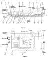
Figure 1 is a side view of an existing device containing electronics and photonics components, with thermoelectric cooling mechanisms; -
Figure 2 is a plan view of the structure ofFigure 1 ; -
Figure 3 is a side view of a device forming a first embodiment of the present invention, including fluidic cooling for cooling a photonic and electronic component assembly; -
Figure 4 is a plan view of the structure ofFigure 3 ; -
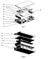
Figure 5 is an exploded view of the structure ofFigure 3 ; -
Figure 6 is a side view of a device forming a second embodiment of the present invention, including fluidic cooling for cooling a photonic and electronic component assembly; -
Figure 7 is an exploded view of the structure ofFigure 6 viewed from above; -
Figure 8 is an exploded view of the structure ofFigure 6 viewed from below; -
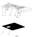
Figure 9 is a plan view showing the base of an hermetic package ofFigure 6 , showing fluid flow connections; -
Figure 10 is a plan view of the structure ofFigure 6 from the underside with base components removed to show fluid flow paths; -
Figure 11 is a perspective view of the fluidic path and reservoir components of the structure ofFigure 6 ; and -
Figure 12 is a schematic view of the device of the first or second embodiments located on a circuit board. - In embodiments, liquid flow cools the internal components of an hermetically sealed container, while maintaining the hermetic seal required for the III-V materials and other internal components. An outer container depending on the application can either be a metallic structure with additional machined features for flow control, or a heat insulating material such as plastic for lower cost packaging integration. Whilst the need for a thermoelectric module is avoided, such a module might additionally be employed to improve operating efficiency. However with fluid flow, an internal thermoelectric module need not be used in the hermetically sealed container, resulting in huge power savings. A fluid layer is provided around the hermetically sealed container for conducting away heat while not interfering with electrical input/output pins and optical path connections, which reduces the ambient influence on the internal temperature of the hermetically sealed container and also enables liquid cooling of a silicon substrate or other thermally conductive substrate to which the silicon photonics is thermally connected.
- In one embodiment of the invention the outer container surrounds the hermetically sealed container and provides a means of bulk heat dissipation, through liquid cooling of the exterior package. The outer container has ports for fluid flow but also slots for input/ output pin connectors. The internal hermetically sealed package has a thermal path to one or more of the other faces allowing for the liquid heat dissipation technique to be employed. Isolation of the internal components from the ambient circuit pack temperature field is done though the use of an insulating layer and a fluidic heat extraction method. The outer structure is a plastic perform with low thermal conductivity but good moisture and solubility repulsion characteristics. The plastic outer structure may also be molded onto the inner package ensuring sufficient sealing at the I/O connections.
- One embodiment has an internal surface within the outer container having formations to control the fluid flow within the outer fluid structure. Protuberance formations are designed to improve the lateral distribution of the flow with minimal pressure drop. These formations ensure a sufficient cross section remains for fluid flow over the range of possible test pressures. On the outlet fluid side these formations are to control the radial flow ensuring that regions of flow do not become stagnant or bypassed, reducing the overall effective heat dissipation of the system. Such internal surface may be a preformed board which is encapsulated in the plastic outer container, ensuring a good seal, thermal isolation and the correct cross-sectional area for the required flow regime.
- In some embodiments, localized regions of increased heat transfer are provided at the base of the package structure. This increased heat transfer is generated by reducing the cross-sectional area (constricting) of the flow hence increasing the velocity. In another embodiment localized cooling regions are generated by thinning of the inner package material.
- One embodiment of the invention has localized fluid connection points in the wall of the hermetic package for attaching a network of fluid flow channels and reservoirs, which are formed within an internal thermal plane, which may be a component substrate, within the hermetically sealed container. Port openings in the internal package allow for fluid to pass from the bulk system cooling to the internal thermal plane. The internal thermal plane includes in its simplest form a number of channels within a thermally conductive substrate assembly, along which the fluid can pass and return back to the bulk system cooling stream. The sealing of this interface between the thermal plane and wall of the sealed container may be implemented by a number of different methods, such as soldering, non-drip connectors, welding, and adhesive bonding. A preferred method is a seal by soldering.
- Another embodiment uses a two phase fluid for thermal control of the internal package structure. This approach through preferential density and surface coatings gives a range of heat transfer locations.
- Referring to
Figures 1 and 2 which show an existing structure containing electronics and photonics components, the structure comprises acasing 2, which forms an hermetically sealed package having at one end an opticalfiber outlet connector 4, and at the opposite end an electrical input/outputterminal pin connector 6. These I/O connectors areas are sealed by a number of different methods, e.g. adhesive bonding, pressurized o-rings, welding, seam sealing. - The hermetic package is necessary on account of the need to provide a controlled atmosphere for the optics components and to protect III-V materials. A first unit mounted within the housing comprises free space optics and
filters 8 mounted on a thermoelectric module structure 8'. A second unit comprisesoptics 10 formed as silicon waveguides (AWG) which are formed on acircuit card 12, so as to conduct light from alaser bar 14, which is mounted on asilicon substrate 16. These items are mounted on a second thermoelectric module 10'. A third unit compriseselectronics components 18, mounted on a thermal spreader, which couples the electronics to the hermetic package walls. In operation, electrical signals applied toterminal 6 are processed inelectronics 18 to provide control signals tolaser bar 14, the lasers therein providing light signals which are conducted through thesilicon waveguide 10 andfree space optics 8 to outputoptical fiber 4. - Typically the thermoelectric module 10' comprises between 100 and 200 of thermoelectric bumps in an area of 15mmx15mm on which silicon
heat spreading bar 16, 10x4 mm, is mounted, but other dimensions may be employed. The laser bar comprises a row of 10 lasers, the lasers being spaced apart by 250 microns. A respective resistive heater is mounted with each laser to individually adjust the temperature of the laser. The package shown inFigures 1 and 2 is very inefficient at maintaining optimum operating temperatures. Typically, the operating environment of an optoelectronics assembly may be around 55°C, whereas the lasers need to be cooled to an operating temperature of 25°C. - Referring now to the first embodiment of the invention shown in
Figures 3, 4 and5 , similar parts to those ofFigures 1 and 2 are denoted by the same reference numeral. An outeropen container 20 of thermally isolating plastic material receives a registeringbase portion 22 of a hermetic package 24 (shown in exploded form inFigure 5 ), of a thermally conductive metallic material. Atop surface 26 of thermally insulating material completes both the hermetic package, and the outer container. The layout of the electronic and photonic components is similar to that ofFigures 1 and 2 , and it may be seen fromFigure 5 that units 8-18 together comprise a singlecomposite assembly 17, with the conductive silicon substrate of each unit 8-18 forming a composite thermallyconductive substrate assembly 19. The substrate assembly may be separate substrate units or joined together units, or be formed as an integral unit. - Fluidic cooling of the components is provided as follows. Between
container structure 20 andbase 22 is provided afluidic passage 28, which permits fluid to flow between afluid inlet 30 and afluid outlet 32 at opposite ends of the tray. The preferred inlet/outlet is an encapsulated ferrule connection encapsulated in the outer plastic packaging during formation. The inlet and outlet fluid connectors are removable and non-dripping. Thebase 22 has recessedportions optics 8,waveguides 12 andlaser bar 14, andelectronics 18. This permits fluid to flow close, at the upper surfaces of the recesses 34-38, to the underside of the electronics and photonic components for cooling. In addition, arrays of streamlined parallel planarfluid flow structures 40 are provided within each recess to direct fluid flow close tobase 22, and to increase fluid flow rate by means of the Bernoulli Effect. - Referring now to the second embodiment shown in
Figures 6 to 11 , similar parts to those ofFigures 3 to 5 are denoted by the same reference numerals. Referring firstly toFigure 8 , theouter container 20 has atop cover 27 of insulating material, withside flanges 29 which overlapbase 20, to completely envelope sealedcontainer 24. In thiscase top 26 ofcontainer 24 may be thermally conductive. For clarity, top 27 is not shown inFigures 6 and7 . - In
Figure 6 ,recess 36 ofFigure 3 has been modified as afirst recess 42 beneathwaveguides 12 separated by an intervening wall from asecond recess 44 disposed beneathlaser bar 14. Although thebase 22 retains the hermetic seal of the first embodiment, the upper floor of each recess is formed with internal inlet and outlet fluid flow paths, directed to the electronics and photonics components. Thus inrecess 38, seeFigures 6 and9 ,fluid flow paths 48 are provided for conducting fluid into contact with electronics components. Inrecess 44,fluid paths 50 are provided which are disposedadjacent laser bar 14. Inrecess 42,fluid paths 52 are provided, disposed directlyadjacent waveguide structure 12. Inrecess 34,fluid paths 56 are provided which are disposed directlyadjacent optics 8. These fluid flow paths 48-56 make sealed connections with fluid flow channels which are formed within the silicon of composite thermal substrate assembly 19 (by known processing techniques), as shown inFigures 10 and11 in particular. These fluid flow channels comprise afluid flow network 62 coupled topaths 48 for contacting the electronic components with cooling fluid. Forlaser bar 14, there arefluid input channels 64 insubstrate 19 to conduct fluid to the laser bar.Fluid outlet channels 66 permit fluid to flow away fromlaser bar 14 back intorecess 42 viapaths 50. -
Fluid flow paths 52 inrecess 42 communicate with areservoir 54 disposed beneathAWG structure 10.Fluid flow paths 56 inrecess 34 communicate with areservoir 58 disposed beneathfree standing optics 8. -
Figure 12 shows thecomplete device 2 of the first or second embodiments, in position mounted on a circuit pack CP. - Advantages of embodiments are reduced power consumption, localized thermal control for local component set points, internal component thermal isolation from the circuit pack ambient, removal of the thermoelectric module, all while maintaining an hermetic seal and the numerous input and output connections. Further advantages are: improved thermal control- maintaining the correct temperature to ensure the correct optical wavelength; improved heat dissipation - extracting larger heat loads from smaller areas; improved thermal isolation - reduced thermal crosstalk across optical signals due to thermal differences, this aspect will improve transition times of operation and allow for greater functionality of the optical components; removal of the thermoelectric module - significantly reducing the overall power consumption of the module; modular assembly - improving the isolation of the interior components from external influences which maintaining a clear heat dissipation path for efficient thermal operation.
- The description and drawings merely illustrate the principles of the invention. It will thus be appreciated that those skilled in the art will be able to devise various arrangements that, although not explicitly described or shown herein, embody the principles of the invention and are included within its spirit and scope. Furthermore, all examples recited herein are principally intended expressly to be only for pedagogical purposes to aid the reader in understanding the principles of the invention and the concepts contributed by the inventor(s) to furthering the art, and are to be construed as being without limitation to such specifically recited examples and conditions. Moreover, all statements herein reciting principles, aspects, and embodiments of the invention, as well as specific examples thereof, are intended to encompass equivalents thereof.
Claims (15)
- A thermal management apparatus for an electrical and/or optical component assembly, comprising:an hermetically sealed container mounted within an outer container,the outer container.having a liquid inlet and a liquid outlet,said outer container and said hermetically sealed container configured to define a liquid path operable to direct a liquid within the outer container and around the hermetically sealed container to remove heat therefrom, andthe hermetically sealed container containing said component assembly, which assembly includes one or more devices, which devices are in thermal communication with a thermally conductive wall portion of said sealed container, whereby said liquid cools said devices.
- A thermal management apparatus according to claim 1 wherein the sealed container has a base portion and side walls of a thermally conductive material.
- A thermal management apparatus according to claim 2, wherein a base and side walls of the outer container are formed of a thermally insulative material.
- A thermal management apparatus according to claim 3, wherein the outer container is formed as a close fit to the sides of the sealed container, or is formed as plastics extrusion moulded to the sealed container.
- A thermal management apparatus according to any of claims 2 to 4, wherein the sealed container and the outer container have a common top portion formed of thermally insulative material, or have separate top portions of conductive and insulative material respectively.
- A thermal management apparatus according to any preceding claim, wherein said one or more devices are mounted on a thermally conductive substrate assembly which is sealed to and in good thermal contact with a base region of the sealed container.
- A thermal management apparatus according to claim 6, wherein said substrate assembly is formed with liquid flow channels which communicate with liquid inlets and outlets in the base region of the sealed container, in order to permit liquid flow from said liquid flow path close to specific photonics devices.
- A thermal management apparatus according to claim 6, wherein said substrate assembly is formed with liquid reservoirs which communicate with liquid inlets and outlets in the base region of the sealed container.
- A thermal management apparatus according to any preceding claim, wherein said outer container has liquid flow structures formed in said liquid flow path to direct liquid flow.
- A thermal management apparatus according to claim 9, including raised liquid flow structures to encourage liquid flow at an increased rate close to specific areas of the base of the sealed container.
- A thermal management apparatus according to claim 11, wherein said raised liquid flow structures are located in one or more recesses of the base of the sealed container.
- A thermal management apparatus according to claim 1, wherein the outer container includes a liquid inlet, which is coupled to a source of cooling liquid, and a liquid outlet.
- A thermal management apparatus according to claim 1, wherein said one of more devices include a photonics device, preferably a laser bar comprising a plurality of lasers.
- Thermal management apparatus for a photonics assembly, comprising an hermetically sealed container mounted within an outer container, and the hermetically sealed container containing a photonics assembly comprising one or more photonics devices, which are mounted on a thermally conductive substrate assembly, which is sealed to and in thermal contact with a wall portion of said sealed container, the thermally conductive substrate assembly having liquid passageways formed therein to permit liquid to flow close to said photonics devices, said wall portion having inlet and outlet liquid paths communicating with said liquid passageways, and the outer container having a liquid inlet and a liquid outlet, so as to provide a cooling liquid flow path between said liquid inlet and outlet via said photonics devices to remove heat therefrom.
- A thermal management apparatus according to claim 13, wherein said liquid passageways include at least one liquid reservoir located beneath at least one photonics device.
Priority Applications (3)
| Application Number | Priority Date | Filing Date | Title |
|---|---|---|---|
| ES11290573T ES2873090T3 (en) | 2011-12-13 | 2011-12-13 | Thermal management of photonic arrays |
| EP11290573.2A EP2605345B1 (en) | 2011-12-13 | 2011-12-13 | Thermal management of photonics assemblies |
| US13/690,450 US9113576B2 (en) | 2011-12-13 | 2012-11-30 | Thermal management of photonics assemblies |
Applications Claiming Priority (1)
| Application Number | Priority Date | Filing Date | Title |
|---|---|---|---|
| EP11290573.2A EP2605345B1 (en) | 2011-12-13 | 2011-12-13 | Thermal management of photonics assemblies |
Publications (2)
| Publication Number | Publication Date |
|---|---|
| EP2605345A1 true EP2605345A1 (en) | 2013-06-19 |
| EP2605345B1 EP2605345B1 (en) | 2021-04-28 |
Family
ID=45440362
Family Applications (1)
| Application Number | Title | Priority Date | Filing Date |
|---|---|---|---|
| EP11290573.2A Active EP2605345B1 (en) | 2011-12-13 | 2011-12-13 | Thermal management of photonics assemblies |
Country Status (3)
| Country | Link |
|---|---|
| US (1) | US9113576B2 (en) |
| EP (1) | EP2605345B1 (en) |
| ES (1) | ES2873090T3 (en) |
Cited By (2)
| Publication number | Priority date | Publication date | Assignee | Title |
|---|---|---|---|---|
| WO2018178745A1 (en) * | 2017-03-29 | 2018-10-04 | Telefonaktiebolaget Lm Ericsson (Publ) | Chip-carrier socket for microfluidic-cooled three-dimensional electronic/photonic integrated circuits |
| US11242189B2 (en) | 2019-11-15 | 2022-02-08 | Yeti Coolers, Llc | Insulating device |
Families Citing this family (27)
| Publication number | Priority date | Publication date | Assignee | Title |
|---|---|---|---|---|
| US9449895B2 (en) * | 2013-05-03 | 2016-09-20 | Infineon Technologies Ag | Cooling system for molded modules and corresponding manufacturing methods |
| JP6345917B2 (en) * | 2013-07-18 | 2018-06-20 | 富士通コンポーネント株式会社 | Optical module |
| US9818671B2 (en) * | 2015-02-10 | 2017-11-14 | Dynatron Corporation | Liquid-cooled heat sink for electronic devices |
| US9613885B2 (en) | 2015-03-03 | 2017-04-04 | Infineon Technologies Ag | Plastic cooler for semiconductor modules |
| EP3417340A1 (en) | 2016-02-16 | 2018-12-26 | NLIGHT, Inc. | Passively aligned single element telescope for improved package brightness |
| WO2017161334A1 (en) | 2016-03-18 | 2017-09-21 | Nlight, Inc. | Spectrally multiplexing diode pump modules to improve brightness |
| US10763640B2 (en) * | 2017-04-24 | 2020-09-01 | Nlight, Inc. | Low swap two-phase cooled diode laser package |
| US10850623B2 (en) | 2017-10-30 | 2020-12-01 | Sf Motors, Inc. | Stacked electric vehicle inverter cells |
| US10833482B2 (en) | 2018-02-06 | 2020-11-10 | Nlight, Inc. | Diode laser apparatus with FAC lens out-of-plane beam steering |
| US10790758B2 (en) | 2018-03-08 | 2020-09-29 | Chongqing Jinkang New Energy Vehicle Co., Ltd. | Power converter for electric vehicle drive systems |
| US10756649B2 (en) | 2018-03-23 | 2020-08-25 | Chongqing Jinkang New Energy Vehicle Co., Ltd. | Inverter module having multiple half-bridge modules for a power converter of an electric vehicle |
| US10779445B2 (en) | 2018-03-23 | 2020-09-15 | Chongqing Jinkang New Energy Vehicle Co., Ltd. | Inverter module having multiple half-bridge modules for a power converter of an electric vehicle |
| US10236791B1 (en) | 2018-03-23 | 2019-03-19 | Sf Motors, Inc. | Inverter module having multiple half-bridge modules for a power converter of an electric vehicle |
| US10778117B2 (en) | 2018-04-17 | 2020-09-15 | Chongqing Jinkang New Energy Vehicle Co., Ltd. | Inverter module of an electric vehicle |
| US10772242B2 (en) | 2018-04-17 | 2020-09-08 | Chongqing Jinkang New Energy Vehicle Co., Ltd. | Inverter module of an electric vehicle |
| US10608423B2 (en) | 2018-04-26 | 2020-03-31 | Sf Motors, Inc. | Electric vehicle inverter module laminated bus bar |
| US10600578B2 (en) | 2018-04-26 | 2020-03-24 | Sf Motors, Inc. | Electric vehicle inverter module capacitors |
| US10660242B2 (en) * | 2018-04-26 | 2020-05-19 | Chongqing Jinkang New Energy Vehicle Co., Ltd. | Electric vehicle inverter module heat sink |
| US10388810B1 (en) | 2018-06-25 | 2019-08-20 | Toyota Motor Engineering & Manufacturing North America, Inc. | Power electronics assemblies having opticondistors and an embedded active cooling chip |
| US10901161B2 (en) * | 2018-09-14 | 2021-01-26 | Toyota Motor Engineering & Manufacturing North America, Inc. | Optical power transfer devices with an embedded active cooling chip |
| US11824323B1 (en) * | 2018-12-06 | 2023-11-21 | Nlight, Inc. | Diode laser package for bidirectionally emitting semiconductor laser devices |
| CN110429457B (en) * | 2019-08-19 | 2024-07-12 | 北京东方锐镭科技有限公司 | Water-cooling heat sink assembly for laser crystal |
| US10943851B1 (en) * | 2019-12-06 | 2021-03-09 | Intel Corporation | Reconstituted wafer assembly |
| RU2754393C1 (en) * | 2020-11-12 | 2021-09-01 | Федеральное государственное бюджетное учреждение науки Физический институт им. П.Н. Лебедева Российской академии наук (ФИАН) | Method for cooling a two-dimensional matrix of laser diodes, a device for its implementation and a connector |
| US12029123B2 (en) * | 2021-01-29 | 2024-07-02 | Taiwan Semiconductor Manufacturing Company, Ltd. | Semiconductor structure and method of manufacturing a semiconductor structure |
| JP7886182B2 (en) * | 2022-05-27 | 2026-07-07 | ニデック株式会社 | Cold Plate |
| CN120092195A (en) * | 2022-10-25 | 2025-06-03 | 3M创新有限公司 | Fiber Optic Feedthrough with Condensation Prevention for Immersion Cooling |
Citations (8)
| Publication number | Priority date | Publication date | Assignee | Title |
|---|---|---|---|---|
| EP0458500A1 (en) * | 1990-05-23 | 1991-11-27 | AT&T Corp. | Circuit pack cooling using turbulators |
| EP0709884A2 (en) * | 1994-10-31 | 1996-05-01 | AT&T Corp. | Microelectronic device having a package with internal ducting for the passage of cooling fluid |
| US5889651A (en) * | 1995-05-31 | 1999-03-30 | Kabushiki Kaisha Toshiba | Circuit board cooling apparatus |
| JP2005045062A (en) * | 2003-07-23 | 2005-02-17 | Seiko Epson Corp | Light source device and projection display device using the same |
| WO2006133238A2 (en) * | 2005-06-07 | 2006-12-14 | Kigre, Inc. | Method for cooling semiconductor laser diodes and light emitting diodes |
| US20080055852A1 (en) * | 2006-09-06 | 2008-03-06 | Airbus Deutschland Gmbh | Aircraft Electronics Cooling Apparatus For An Aircraft Having A Liquid Cooling System |
| JP2008235139A (en) * | 2007-03-23 | 2008-10-02 | Kaneka Corp | Aging device of organic el device and its method |
| JP2008244182A (en) * | 2007-03-28 | 2008-10-09 | Kaneka Corp | High-intensity light emitting organic el light-emitting device |
Family Cites Families (33)
| Publication number | Priority date | Publication date | Assignee | Title |
|---|---|---|---|---|
| US4805420A (en) * | 1987-06-22 | 1989-02-21 | Ncr Corporation | Cryogenic vessel for cooling electronic components |
| US6729383B1 (en) * | 1999-12-16 | 2004-05-04 | The United States Of America As Represented By The Secretary Of The Navy | Fluid-cooled heat sink with turbulence-enhancing support pins |
| JP2003060371A (en) * | 2001-08-16 | 2003-02-28 | Nec Corp | Heat dissipation structure of communication equipment housing |
| US6744136B2 (en) * | 2001-10-29 | 2004-06-01 | International Rectifier Corporation | Sealed liquid cooled electronic device |
| DE10317580B4 (en) * | 2002-04-18 | 2010-09-16 | Hitachi, Ltd. | Electric inverter device with a liquid channel and electric vehicle with such an inverter device |
| KR20040006636A (en) * | 2002-07-13 | 2004-01-24 | 천기완 | The soft cooling jacket for water cooling of the electronics and buffer jacket using of it |
| US7167366B2 (en) * | 2002-09-11 | 2007-01-23 | Kioan Cheon | Soft cooling jacket for electronic device |
| US7104312B2 (en) * | 2002-11-01 | 2006-09-12 | Cooligy, Inc. | Method and apparatus for achieving temperature uniformity and hot spot cooling in a heat producing device |
| US7431071B2 (en) * | 2003-10-15 | 2008-10-07 | Thermal Corp. | Fluid circuit heat transfer device for plural heat sources |
| US7254024B2 (en) * | 2004-05-11 | 2007-08-07 | Salmon Peter C | Cooling apparatus and method |
| JP4256310B2 (en) * | 2004-06-30 | 2009-04-22 | 株式会社東芝 | Electronics |
| US20060162903A1 (en) * | 2005-01-21 | 2006-07-27 | Bhatti Mohinder S | Liquid cooled thermosiphon with flexible partition |
| US7506682B2 (en) * | 2005-01-21 | 2009-03-24 | Delphi Technologies, Inc. | Liquid cooled thermosiphon for electronic components |
| US7077189B1 (en) * | 2005-01-21 | 2006-07-18 | Delphi Technologies, Inc. | Liquid cooled thermosiphon with flexible coolant tubes |
| US7604040B2 (en) * | 2005-06-15 | 2009-10-20 | Coolit Systems Inc. | Integrated liquid cooled heat sink for electronic components |
| CN100499974C (en) * | 2005-08-10 | 2009-06-10 | 富准精密工业(深圳)有限公司 | Integral liquid-cooled radiator |
| US7705342B2 (en) * | 2005-09-16 | 2010-04-27 | University Of Cincinnati | Porous semiconductor-based evaporator having porous and non-porous regions, the porous regions having through-holes |
| US8174828B2 (en) * | 2006-02-06 | 2012-05-08 | Parker-Hannifin Corporation | Narrow gap spray cooling in a globally cooled enclosure |
| US7495914B2 (en) * | 2006-02-06 | 2009-02-24 | Isothermal Systems Research, Inc. | Narrow gap spray cooling in a globally cooled enclosure |
| US7551439B2 (en) * | 2006-03-28 | 2009-06-23 | Delphi Technologies, Inc. | Fluid cooled electronic assembly |
| US8174830B2 (en) * | 2008-05-06 | 2012-05-08 | Rockwell Collins, Inc. | System and method for a substrate with internal pumped liquid metal for thermal spreading and cooling |
| US7753662B2 (en) * | 2006-09-21 | 2010-07-13 | Fu Zhun Precision Industry (Shen Zhen) Co., Ltd. | Miniature liquid cooling device having an integral pump therein |
| US7285851B1 (en) * | 2006-09-29 | 2007-10-23 | Teradyne, Inc. | Liquid immersion cooled multichip module |
| US7762314B2 (en) * | 2007-04-24 | 2010-07-27 | International Business Machines Corporation | Cooling apparatus, cooled electronic module and methods of fabrication employing a manifold structure with interleaved coolant inlet and outlet passageways |
| US7731079B2 (en) * | 2008-06-20 | 2010-06-08 | International Business Machines Corporation | Cooling apparatus and method of fabrication thereof with a cold plate formed in situ on a surface to be cooled |
| CN101610664B (en) * | 2008-06-20 | 2014-05-14 | 萨帕铝型材(上海)有限公司 | Liquid cooler and manufacture method thereof |
| US20100085713A1 (en) * | 2008-10-03 | 2010-04-08 | Balandin Alexander A | Lateral graphene heat spreaders for electronic and optoelectronic devices and circuits |
| US7961475B2 (en) * | 2008-10-23 | 2011-06-14 | International Business Machines Corporation | Apparatus and method for facilitating immersion-cooling of an electronic subsystem |
| US8081463B2 (en) * | 2009-06-16 | 2011-12-20 | Asia Vital Components Co., Ltd. | Water-cooled communication chassis |
| JP5702988B2 (en) * | 2010-01-29 | 2015-04-15 | 株式会社 日立パワーデバイス | SEMICONDUCTOR POWER MODULE, POWER CONVERSION DEVICE MOUNTED WITH THE SEMICONDUCTOR POWER MODULE, AND METHOD FOR MANUFACTURING SEMICONDUCTOR POWER MODULE WATER CHANNEL FORMING BODY |
| JP5423654B2 (en) * | 2010-02-05 | 2014-02-19 | 株式会社デンソー | Power converter |
| US20110313576A1 (en) * | 2010-06-17 | 2011-12-22 | Mark Randal Nicewonger | System and method for flowing fluids through electronic chassis modules |
| CN102300442A (en) * | 2010-06-25 | 2011-12-28 | 鸿富锦精密工业(深圳)有限公司 | Liquid-cooled radiating system and electronic device using same |
-
2011
- 2011-12-13 ES ES11290573T patent/ES2873090T3/en active Active
- 2011-12-13 EP EP11290573.2A patent/EP2605345B1/en active Active
-
2012
- 2012-11-30 US US13/690,450 patent/US9113576B2/en active Active
Patent Citations (8)
| Publication number | Priority date | Publication date | Assignee | Title |
|---|---|---|---|---|
| EP0458500A1 (en) * | 1990-05-23 | 1991-11-27 | AT&T Corp. | Circuit pack cooling using turbulators |
| EP0709884A2 (en) * | 1994-10-31 | 1996-05-01 | AT&T Corp. | Microelectronic device having a package with internal ducting for the passage of cooling fluid |
| US5889651A (en) * | 1995-05-31 | 1999-03-30 | Kabushiki Kaisha Toshiba | Circuit board cooling apparatus |
| JP2005045062A (en) * | 2003-07-23 | 2005-02-17 | Seiko Epson Corp | Light source device and projection display device using the same |
| WO2006133238A2 (en) * | 2005-06-07 | 2006-12-14 | Kigre, Inc. | Method for cooling semiconductor laser diodes and light emitting diodes |
| US20080055852A1 (en) * | 2006-09-06 | 2008-03-06 | Airbus Deutschland Gmbh | Aircraft Electronics Cooling Apparatus For An Aircraft Having A Liquid Cooling System |
| JP2008235139A (en) * | 2007-03-23 | 2008-10-02 | Kaneka Corp | Aging device of organic el device and its method |
| JP2008244182A (en) * | 2007-03-28 | 2008-10-09 | Kaneka Corp | High-intensity light emitting organic el light-emitting device |
Non-Patent Citations (1)
| Title |
|---|
| DIERL B ET AL: "TEMPERATURE EXCHANGE FOR ELECTRICAL AND MECHANICAL COMPONENTS", IBM TECHNICAL DISCLOSURE BULLETIN, INTERNATIONAL BUSINESS MACHINES CORP. (THORNWOOD), US, vol. 19, no. 10, 1 March 1977 (1977-03-01), XP002071530, ISSN: 0018-8689 * |
Cited By (3)
| Publication number | Priority date | Publication date | Assignee | Title |
|---|---|---|---|---|
| WO2018178745A1 (en) * | 2017-03-29 | 2018-10-04 | Telefonaktiebolaget Lm Ericsson (Publ) | Chip-carrier socket for microfluidic-cooled three-dimensional electronic/photonic integrated circuits |
| US11562942B2 (en) | 2017-03-29 | 2023-01-24 | Telefonaktiebolaget Lm Ericsson (Publ) | Chip-carrier socket for microfluidic-cooled three-dimensional electronic/photonic integrated circuits |
| US11242189B2 (en) | 2019-11-15 | 2022-02-08 | Yeti Coolers, Llc | Insulating device |
Also Published As
| Publication number | Publication date |
|---|---|
| US9113576B2 (en) | 2015-08-18 |
| US20130146253A1 (en) | 2013-06-13 |
| ES2873090T3 (en) | 2021-11-03 |
| EP2605345B1 (en) | 2021-04-28 |
Similar Documents
| Publication | Publication Date | Title |
|---|---|---|
| US9113576B2 (en) | Thermal management of photonics assemblies | |
| EP1378153B1 (en) | Electronic module including a cooling substrate and manufacturing method thereof | |
| Enright et al. | A vision for thermally integrated photonics systems | |
| EP3454370B1 (en) | Package, and method of manufacturing a package comprising an enclosure and an integrated circuit | |
| US11562942B2 (en) | Chip-carrier socket for microfluidic-cooled three-dimensional electronic/photonic integrated circuits | |
| EP1362370A2 (en) | Electronic device using evaporative micro-cooling and associated methods | |
| US12313891B2 (en) | Thermal management system for multi-chip-module and associated methods | |
| AU2002306686B2 (en) | Electronic module with fluid dissociation electrodes and methods | |
| US12114416B2 (en) | Heat removal from silicon photonics chip using a recessed side-by-side thermal dissipation layout | |
| CN113056159A (en) | Universal cooling substrate module | |
| AU2002254176A1 (en) | Electronic module including a cooling substrate and related methods | |
| US11561353B2 (en) | Optical circuit | |
| AU2002306686A1 (en) | Electronic module with fluid dissociation electrodes and methods | |
| EP2866313A1 (en) | Integrated circuit | |
| Punch | Thermal challenges in photonic integrated circuits | |
| JP2001177031A (en) | Optical transceiver with cooling device | |
| CN104718672B (en) | Photoelectric components | |
| Tang et al. | Thermal management solutions and design guidelines for silicon based photonic integrated modules | |
| CN117293104B (en) | SIC device heat dissipation packaging structure and packaging method | |
| Salamon | Challenges and opportunities for thermal management of information and communications technologies equipment: a telecommunications perspective | |
| O'Connor et al. | The thermal behavior of a flip-chip laser array within a photonics integrated circuit (PIC) | |
| CN218570729U (en) | Heat dissipation device and equipment | |
| EP4050389A1 (en) | Apparatus for integrating an electronic integrated circuit and a photonic integrated circuit | |
| GB2392551A (en) | Optical chip unit | |
| GB2392552A (en) | Thermal isolation of optical chips |
Legal Events
| Date | Code | Title | Description |
|---|---|---|---|
| PUAI | Public reference made under article 153(3) epc to a published international application that has entered the european phase |
Free format text: ORIGINAL CODE: 0009012 |
|
| AK | Designated contracting states |
Kind code of ref document: A1 Designated state(s): AL AT BE BG CH CY CZ DE DK EE ES FI FR GB GR HR HU IE IS IT LI LT LU LV MC MK MT NL NO PL PT RO RS SE SI SK SM TR |
|
| AX | Request for extension of the european patent |
Extension state: BA ME |
|
| 111Z | Information provided on other rights and legal means of execution |
Free format text: AL AT BE BG CH CY CZ DE DK EE ES FI FR GB GR HR HU IE IS IT LI LT LU LV MC MK MT NL NO PL PT RO RS SE SI SK SM TR Effective date: 20130410 |
|
| 17P | Request for examination filed |
Effective date: 20131219 |
|
| RBV | Designated contracting states (corrected) |
Designated state(s): AL AT BE BG CH CY CZ DE DK EE ES FI FR GB GR HR HU IE IS IT LI LT LU LV MC MK MT NL NO PL PT RO RS SE SI SK SM TR |
|
| RAP1 | Party data changed (applicant data changed or rights of an application transferred) |
Owner name: ALCATEL LUCENT |
|
| D11X | Information provided on other rights and legal means of execution (deleted) | ||
| STAA | Information on the status of an ep patent application or granted ep patent |
Free format text: STATUS: EXAMINATION IS IN PROGRESS |
|
| 17Q | First examination report despatched |
Effective date: 20171019 |
|
| RAP1 | Party data changed (applicant data changed or rights of an application transferred) |
Owner name: ALCATEL LUCENT |
|
| GRAP | Despatch of communication of intention to grant a patent |
Free format text: ORIGINAL CODE: EPIDOSNIGR1 |
|
| STAA | Information on the status of an ep patent application or granted ep patent |
Free format text: STATUS: GRANT OF PATENT IS INTENDED |
|
| RIC1 | Information provided on ipc code assigned before grant |
Ipc: H01S 3/04 20060101ALN20201012BHEP Ipc: H01S 5/024 20060101AFI20201012BHEP Ipc: H01L 23/473 20060101ALI20201012BHEP |
|
| RIC1 | Information provided on ipc code assigned before grant |
Ipc: H01S 5/024 20060101AFI20201023BHEP Ipc: H01S 3/04 20060101ALN20201023BHEP Ipc: H01L 23/473 20060101ALI20201023BHEP |
|
| INTG | Intention to grant announced |
Effective date: 20201116 |
|
| GRAS | Grant fee paid |
Free format text: ORIGINAL CODE: EPIDOSNIGR3 |
|
| GRAA | (expected) grant |
Free format text: ORIGINAL CODE: 0009210 |
|
| STAA | Information on the status of an ep patent application or granted ep patent |
Free format text: STATUS: THE PATENT HAS BEEN GRANTED |
|
| AK | Designated contracting states |
Kind code of ref document: B1 Designated state(s): AL AT BE BG CH CY CZ DE DK EE ES FI FR GB GR HR HU IE IS IT LI LT LU LV MC MK MT NL NO PL PT RO RS SE SI SK SM TR |
|
| REG | Reference to a national code |
Ref country code: GB Ref legal event code: FG4D |
|
| REG | Reference to a national code |
Ref country code: CH Ref legal event code: EP |
|
| REG | Reference to a national code |
Ref country code: DE Ref legal event code: R096 Ref document number: 602011070808 Country of ref document: DE |
|
| REG | Reference to a national code |
Ref country code: AT Ref legal event code: REF Ref document number: 1388195 Country of ref document: AT Kind code of ref document: T Effective date: 20210515 |
|
| REG | Reference to a national code |
Ref country code: IE Ref legal event code: FG4D |
|
| REG | Reference to a national code |
Ref country code: NL Ref legal event code: FP |
|
| REG | Reference to a national code |
Ref country code: LT Ref legal event code: MG9D |
|
| REG | Reference to a national code |
Ref country code: AT Ref legal event code: MK05 Ref document number: 1388195 Country of ref document: AT Kind code of ref document: T Effective date: 20210428 |
|
| PG25 | Lapsed in a contracting state [announced via postgrant information from national office to epo] |
Ref country code: FI Free format text: LAPSE BECAUSE OF FAILURE TO SUBMIT A TRANSLATION OF THE DESCRIPTION OR TO PAY THE FEE WITHIN THE PRESCRIBED TIME-LIMIT Effective date: 20210428 Ref country code: LT Free format text: LAPSE BECAUSE OF FAILURE TO SUBMIT A TRANSLATION OF THE DESCRIPTION OR TO PAY THE FEE WITHIN THE PRESCRIBED TIME-LIMIT Effective date: 20210428 Ref country code: AT Free format text: LAPSE BECAUSE OF FAILURE TO SUBMIT A TRANSLATION OF THE DESCRIPTION OR TO PAY THE FEE WITHIN THE PRESCRIBED TIME-LIMIT Effective date: 20210428 Ref country code: BG Free format text: LAPSE BECAUSE OF FAILURE TO SUBMIT A TRANSLATION OF THE DESCRIPTION OR TO PAY THE FEE WITHIN THE PRESCRIBED TIME-LIMIT Effective date: 20210728 Ref country code: HR Free format text: LAPSE BECAUSE OF FAILURE TO SUBMIT A TRANSLATION OF THE DESCRIPTION OR TO PAY THE FEE WITHIN THE PRESCRIBED TIME-LIMIT Effective date: 20210428 |
|
| REG | Reference to a national code |
Ref country code: ES Ref legal event code: FG2A Ref document number: 2873090 Country of ref document: ES Kind code of ref document: T3 Effective date: 20211103 |
|
| PG25 | Lapsed in a contracting state [announced via postgrant information from national office to epo] |
Ref country code: SE Free format text: LAPSE BECAUSE OF FAILURE TO SUBMIT A TRANSLATION OF THE DESCRIPTION OR TO PAY THE FEE WITHIN THE PRESCRIBED TIME-LIMIT Effective date: 20210428 Ref country code: RS Free format text: LAPSE BECAUSE OF FAILURE TO SUBMIT A TRANSLATION OF THE DESCRIPTION OR TO PAY THE FEE WITHIN THE PRESCRIBED TIME-LIMIT Effective date: 20210428 Ref country code: LV Free format text: LAPSE BECAUSE OF FAILURE TO SUBMIT A TRANSLATION OF THE DESCRIPTION OR TO PAY THE FEE WITHIN THE PRESCRIBED TIME-LIMIT Effective date: 20210428 Ref country code: GR Free format text: LAPSE BECAUSE OF FAILURE TO SUBMIT A TRANSLATION OF THE DESCRIPTION OR TO PAY THE FEE WITHIN THE PRESCRIBED TIME-LIMIT Effective date: 20210729 Ref country code: IS Free format text: LAPSE BECAUSE OF FAILURE TO SUBMIT A TRANSLATION OF THE DESCRIPTION OR TO PAY THE FEE WITHIN THE PRESCRIBED TIME-LIMIT Effective date: 20210828 Ref country code: PT Free format text: LAPSE BECAUSE OF FAILURE TO SUBMIT A TRANSLATION OF THE DESCRIPTION OR TO PAY THE FEE WITHIN THE PRESCRIBED TIME-LIMIT Effective date: 20210830 Ref country code: PL Free format text: LAPSE BECAUSE OF FAILURE TO SUBMIT A TRANSLATION OF THE DESCRIPTION OR TO PAY THE FEE WITHIN THE PRESCRIBED TIME-LIMIT Effective date: 20210428 Ref country code: NO Free format text: LAPSE BECAUSE OF FAILURE TO SUBMIT A TRANSLATION OF THE DESCRIPTION OR TO PAY THE FEE WITHIN THE PRESCRIBED TIME-LIMIT Effective date: 20210728 |
|
| PG25 | Lapsed in a contracting state [announced via postgrant information from national office to epo] |
Ref country code: EE Free format text: LAPSE BECAUSE OF FAILURE TO SUBMIT A TRANSLATION OF THE DESCRIPTION OR TO PAY THE FEE WITHIN THE PRESCRIBED TIME-LIMIT Effective date: 20210428 Ref country code: CZ Free format text: LAPSE BECAUSE OF FAILURE TO SUBMIT A TRANSLATION OF THE DESCRIPTION OR TO PAY THE FEE WITHIN THE PRESCRIBED TIME-LIMIT Effective date: 20210428 Ref country code: DK Free format text: LAPSE BECAUSE OF FAILURE TO SUBMIT A TRANSLATION OF THE DESCRIPTION OR TO PAY THE FEE WITHIN THE PRESCRIBED TIME-LIMIT Effective date: 20210428 Ref country code: SM Free format text: LAPSE BECAUSE OF FAILURE TO SUBMIT A TRANSLATION OF THE DESCRIPTION OR TO PAY THE FEE WITHIN THE PRESCRIBED TIME-LIMIT Effective date: 20210428 Ref country code: SK Free format text: LAPSE BECAUSE OF FAILURE TO SUBMIT A TRANSLATION OF THE DESCRIPTION OR TO PAY THE FEE WITHIN THE PRESCRIBED TIME-LIMIT Effective date: 20210428 Ref country code: RO Free format text: LAPSE BECAUSE OF FAILURE TO SUBMIT A TRANSLATION OF THE DESCRIPTION OR TO PAY THE FEE WITHIN THE PRESCRIBED TIME-LIMIT Effective date: 20210428 |
|
| REG | Reference to a national code |
Ref country code: DE Ref legal event code: R097 Ref document number: 602011070808 Country of ref document: DE |
|
| PLBE | No opposition filed within time limit |
Free format text: ORIGINAL CODE: 0009261 |
|
| STAA | Information on the status of an ep patent application or granted ep patent |
Free format text: STATUS: NO OPPOSITION FILED WITHIN TIME LIMIT |
|
| 26N | No opposition filed |
Effective date: 20220131 |
|
| PG25 | Lapsed in a contracting state [announced via postgrant information from national office to epo] |
Ref country code: IS Free format text: LAPSE BECAUSE OF FAILURE TO SUBMIT A TRANSLATION OF THE DESCRIPTION OR TO PAY THE FEE WITHIN THE PRESCRIBED TIME-LIMIT Effective date: 20210828 Ref country code: AL Free format text: LAPSE BECAUSE OF FAILURE TO SUBMIT A TRANSLATION OF THE DESCRIPTION OR TO PAY THE FEE WITHIN THE PRESCRIBED TIME-LIMIT Effective date: 20210428 |
|
| PG25 | Lapsed in a contracting state [announced via postgrant information from national office to epo] |
Ref country code: MC Free format text: LAPSE BECAUSE OF FAILURE TO SUBMIT A TRANSLATION OF THE DESCRIPTION OR TO PAY THE FEE WITHIN THE PRESCRIBED TIME-LIMIT Effective date: 20210428 Ref country code: IT Free format text: LAPSE BECAUSE OF FAILURE TO SUBMIT A TRANSLATION OF THE DESCRIPTION OR TO PAY THE FEE WITHIN THE PRESCRIBED TIME-LIMIT Effective date: 20210428 |
|
| REG | Reference to a national code |
Ref country code: CH Ref legal event code: PL |
|
| REG | Reference to a national code |
Ref country code: BE Ref legal event code: MM Effective date: 20211231 |
|
| PG25 | Lapsed in a contracting state [announced via postgrant information from national office to epo] |
Ref country code: LU Free format text: LAPSE BECAUSE OF NON-PAYMENT OF DUE FEES Effective date: 20211213 Ref country code: IE Free format text: LAPSE BECAUSE OF NON-PAYMENT OF DUE FEES Effective date: 20211213 |
|
| PG25 | Lapsed in a contracting state [announced via postgrant information from national office to epo] |
Ref country code: BE Free format text: LAPSE BECAUSE OF NON-PAYMENT OF DUE FEES Effective date: 20211231 |
|
| PG25 | Lapsed in a contracting state [announced via postgrant information from national office to epo] |
Ref country code: LI Free format text: LAPSE BECAUSE OF NON-PAYMENT OF DUE FEES Effective date: 20211231 Ref country code: CH Free format text: LAPSE BECAUSE OF NON-PAYMENT OF DUE FEES Effective date: 20211231 |
|
| PG25 | Lapsed in a contracting state [announced via postgrant information from national office to epo] |
Ref country code: HU Free format text: LAPSE BECAUSE OF FAILURE TO SUBMIT A TRANSLATION OF THE DESCRIPTION OR TO PAY THE FEE WITHIN THE PRESCRIBED TIME-LIMIT; INVALID AB INITIO Effective date: 20111213 Ref country code: CY Free format text: LAPSE BECAUSE OF FAILURE TO SUBMIT A TRANSLATION OF THE DESCRIPTION OR TO PAY THE FEE WITHIN THE PRESCRIBED TIME-LIMIT Effective date: 20210428 |
|
| P01 | Opt-out of the competence of the unified patent court (upc) registered |
Effective date: 20230606 |
|
| PG25 | Lapsed in a contracting state [announced via postgrant information from national office to epo] |
Ref country code: MK Free format text: LAPSE BECAUSE OF FAILURE TO SUBMIT A TRANSLATION OF THE DESCRIPTION OR TO PAY THE FEE WITHIN THE PRESCRIBED TIME-LIMIT Effective date: 20210428 |
|
| PG25 | Lapsed in a contracting state [announced via postgrant information from national office to epo] |
Ref country code: MT Free format text: LAPSE BECAUSE OF FAILURE TO SUBMIT A TRANSLATION OF THE DESCRIPTION OR TO PAY THE FEE WITHIN THE PRESCRIBED TIME-LIMIT Effective date: 20210428 |
|
| PG25 | Lapsed in a contracting state [announced via postgrant information from national office to epo] |
Ref country code: TR Free format text: LAPSE BECAUSE OF FAILURE TO SUBMIT A TRANSLATION OF THE DESCRIPTION OR TO PAY THE FEE WITHIN THE PRESCRIBED TIME-LIMIT Effective date: 20210428 |
|
| PGFP | Annual fee paid to national office [announced via postgrant information from national office to epo] |
Ref country code: NL Payment date: 20260526 Year of fee payment: 15 |
|
| PGFP | Annual fee paid to national office [announced via postgrant information from national office to epo] |
Ref country code: ES Payment date: 20260504 Year of fee payment: 15 |
|
| PGFP | Annual fee paid to national office [announced via postgrant information from national office to epo] |
Ref country code: GB Payment date: 20260527 Year of fee payment: 15 |
|
| PGFP | Annual fee paid to national office [announced via postgrant information from national office to epo] |
Ref country code: DE Payment date: 20260528 Year of fee payment: 15 |
|
| PGFP | Annual fee paid to national office [announced via postgrant information from national office to epo] |
Ref country code: FR Payment date: 20260525 Year of fee payment: 15 |