EP2603063A1 - Printed circuit board - Google Patents
Printed circuit board Download PDFInfo
- Publication number
- EP2603063A1 EP2603063A1 EP12191363.6A EP12191363A EP2603063A1 EP 2603063 A1 EP2603063 A1 EP 2603063A1 EP 12191363 A EP12191363 A EP 12191363A EP 2603063 A1 EP2603063 A1 EP 2603063A1
- Authority
- EP
- European Patent Office
- Prior art keywords
- semiconductor package
- region
- wiring board
- printed wiring
- solder ball
- Prior art date
- Legal status (The legal status is an assumption and is not a legal conclusion. Google has not performed a legal analysis and makes no representation as to the accuracy of the status listed.)
- Withdrawn
Links
Images



Classifications
-
- H—ELECTRICITY
- H05—ELECTRIC TECHNIQUES NOT OTHERWISE PROVIDED FOR
- H05K—PRINTED CIRCUITS; CASINGS OR CONSTRUCTIONAL DETAILS OF ELECTRIC APPARATUS; MANUFACTURE OF ASSEMBLAGES OF ELECTRICAL COMPONENTS
- H05K1/00—Printed circuits
- H05K1/02—Details
- H05K1/0271—Arrangements for reducing stress or warp in rigid printed circuit boards, e.g. caused by loads, vibrations or differences in thermal expansion
-
- H—ELECTRICITY
- H05—ELECTRIC TECHNIQUES NOT OTHERWISE PROVIDED FOR
- H05K—PRINTED CIRCUITS; CASINGS OR CONSTRUCTIONAL DETAILS OF ELECTRIC APPARATUS; MANUFACTURE OF ASSEMBLAGES OF ELECTRICAL COMPONENTS
- H05K1/00—Printed circuits
- H05K1/18—Printed circuits structurally associated with non-printed electric components
- H05K1/181—Printed circuits structurally associated with non-printed electric components associated with surface mounted components
-
- H—ELECTRICITY
- H05—ELECTRIC TECHNIQUES NOT OTHERWISE PROVIDED FOR
- H05K—PRINTED CIRCUITS; CASINGS OR CONSTRUCTIONAL DETAILS OF ELECTRIC APPARATUS; MANUFACTURE OF ASSEMBLAGES OF ELECTRICAL COMPONENTS
- H05K2201/00—Indexing scheme relating to printed circuits covered by H05K1/00
- H05K2201/06—Thermal details
- H05K2201/068—Thermal details wherein the coefficient of thermal expansion is important
-
- H—ELECTRICITY
- H05—ELECTRIC TECHNIQUES NOT OTHERWISE PROVIDED FOR
- H05K—PRINTED CIRCUITS; CASINGS OR CONSTRUCTIONAL DETAILS OF ELECTRIC APPARATUS; MANUFACTURE OF ASSEMBLAGES OF ELECTRICAL COMPONENTS
- H05K2201/00—Indexing scheme relating to printed circuits covered by H05K1/00
- H05K2201/10—Details of components or other objects attached to or integrated in a printed circuit board
- H05K2201/10431—Details of mounted components
- H05K2201/10507—Involving several components
- H05K2201/10545—Related components mounted on both sides of the PCB
-
- H—ELECTRICITY
- H05—ELECTRIC TECHNIQUES NOT OTHERWISE PROVIDED FOR
- H05K—PRINTED CIRCUITS; CASINGS OR CONSTRUCTIONAL DETAILS OF ELECTRIC APPARATUS; MANUFACTURE OF ASSEMBLAGES OF ELECTRICAL COMPONENTS
- H05K2201/00—Indexing scheme relating to printed circuits covered by H05K1/00
- H05K2201/10—Details of components or other objects attached to or integrated in a printed circuit board
- H05K2201/10613—Details of electrical connections of non-printed components, e.g. special leads
- H05K2201/10621—Components characterised by their electrical contacts
- H05K2201/10734—Ball grid array [BGA]; Bump grid array
-
- H—ELECTRICITY
- H10—SEMICONDUCTOR DEVICES; ELECTRIC SOLID-STATE DEVICES NOT OTHERWISE PROVIDED FOR
- H10W—GENERIC PACKAGES, INTERCONNECTIONS, CONNECTORS OR OTHER CONSTRUCTIONAL DETAILS OF DEVICES COVERED BY CLASS H10
- H10W70/00—Package substrates; Interposers; Redistribution layers [RDL]
- H10W70/60—Insulating or insulated package substrates; Interposers; Redistribution layers
-
- H—ELECTRICITY
- H10—SEMICONDUCTOR DEVICES; ELECTRIC SOLID-STATE DEVICES NOT OTHERWISE PROVIDED FOR
- H10W—GENERIC PACKAGES, INTERCONNECTIONS, CONNECTORS OR OTHER CONSTRUCTIONAL DETAILS OF DEVICES COVERED BY CLASS H10
- H10W90/00—Package configurations
- H10W90/701—Package configurations characterised by the relative positions of pads or connectors relative to package parts
- H10W90/721—Package configurations characterised by the relative positions of pads or connectors relative to package parts of bump connectors
- H10W90/724—Package configurations characterised by the relative positions of pads or connectors relative to package parts of bump connectors between a chip and a stacked insulating package substrate, interposer or RDL
-
- Y—GENERAL TAGGING OF NEW TECHNOLOGICAL DEVELOPMENTS; GENERAL TAGGING OF CROSS-SECTIONAL TECHNOLOGIES SPANNING OVER SEVERAL SECTIONS OF THE IPC; TECHNICAL SUBJECTS COVERED BY FORMER USPC CROSS-REFERENCE ART COLLECTIONS [XRACs] AND DIGESTS
- Y02—TECHNOLOGIES OR APPLICATIONS FOR MITIGATION OR ADAPTATION AGAINST CLIMATE CHANGE
- Y02P—CLIMATE CHANGE MITIGATION TECHNOLOGIES IN THE PRODUCTION OR PROCESSING OF GOODS
- Y02P70/00—Climate change mitigation technologies in the production process for final industrial or consumer products
- Y02P70/50—Manufacturing or production processes characterised by the final manufactured product
Definitions
- the present invention relates to a printed circuit board in which semiconductor packages are mounted on a printed wiring board.
- the present invention relates to a printed circuit board in which semiconductor packages are mounted on front and back sides of a printed wiring board such that they face each other.
- quad flat packages QFPs
- lead terminals therearound
- CSP chip size package
- turning on the electronic apparatus causes semiconductor devices included in the semiconductor packages to generate heat.
- the heat generated by the semiconductor devices causes expansion and deformation of the semiconductor packages and the printed wiring board having the semiconductor packages mounted thereon.
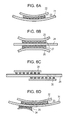
- Fig. 6A illustrates a printed circuit board in which a semiconductor package is mounted only on one side of a printed wiring board.
- the printed circuit board illustrated in Fig. 6A includes a printed wiring board 21, a semiconductor package 22 having a semiconductor device (not shown) mounted therein, and solder ball electrodes 23 serving as connection terminals for joining the printed wiring board 21 to the semiconductor package 22.
- heat generated by the semiconductor device mounted in the semiconductor package 22 causes expansion of the semiconductor package 22 and the printed wiring board 21. Due to a difference in coefficient of linear expansion between the semiconductor package 22 and the printed wiring board 21, stress is applied to the solder ball electrodes 23.
- the semiconductor package 22 and the printed wiring board 21 having the semiconductor package 22 mounted thereon warp to reduce the stress applied to the solder ball electrodes 23.
- the coefficient of linear expansion of the semiconductor package 22 in which the semiconductor device made of silicon is mounted is smaller than that of the printed wiring board 21 made of glass epoxy resin or the like. Therefore, as illustrated in Fig. 6A , the semiconductor package 22 and the printed wiring board 21 having the semiconductor package 22 mounted thereon warp together to be raised at both ends (or warp upward).
- Fig. 6B is a cross-sectional view of a printed circuit board in which two identical semiconductor packages are mounted on both sides of a printed wiring board such that they face each other.
- the printed circuit board illustrated in Fig. 6B includes a printed wiring board 24, semiconductor packages 25 and 26 each having a semiconductor device (not shown) mounted therein, and solder ball electrodes 27 for joining the printed wiring board 24 to both of the semiconductor packages 25 and 26.
- heat generated by the semiconductor devices mounted in the semiconductor packages 25 and 26 causes expansion of the semiconductor packages 25 and 26 and the printed wiring board 24.
- stress is applied to the solder ball electrodes 27. This causes the semiconductor packages 25 and 26 to warp upward and downward, respectively.
- the printed wiring board 24 is unable to warp. Therefore, the stress applied to the solder ball electrodes 27 is not reduced and accumulates in the solder ball electrodes 27. This significantly degrades the joint reliability of the solder ball electrodes 27.
- Japanese Patent Laid-Open No. 2004-273617 discloses a configuration in which, as illustrated in Fig. 6C , semiconductor packages 29 and 30 are mounted on the front and back sides of a printed wiring board 28 such that they partially face each other.
- BGA semiconductor packages with much smaller sizes than before have been increasingly used in recent years.
- small-sized semiconductor packages are smaller in the diameter of solder ball electrodes, smaller in the area of connection pads, smaller in the number of solder ball electrodes, and thus lower in the strength of joining to the printed wiring board. Additionally, due to their thinner substrates, small-sized semiconductor packages are less rigid than large-sized semiconductor packages.
- Fig. 6D illustrates a printed circuit board in which a small-sized semiconductor package and a normal-sized semiconductor package are mounted on both sides of a printed wiring board such that they face each other.
- the printed circuit board illustrated in Fig. 6D includes a printed wiring board 31, a semiconductor package 32 having a semiconductor device (not shown) mounted therein, solder ball electrodes 33 serving as connection terminals for joining the printed wiring board 31 to the semiconductor package 32, a small-sized semiconductor package 34 having a semiconductor device (not shown) mounted therein and a smaller number of connected terminals than the semiconductor package 32, and solder ball electrodes 35 serving as connection terminals for joining the printed wiring board 31 to the small-sized semiconductor package 34.
- solder ball electrodes 35 serving as connection terminals for joining the printed wiring board 31 to the small-sized semiconductor package 34.
- the printed wiring board 31 warps to be raised at both ends (or warps upward), whereas the small-sized semiconductor package 34 warps to be lowered at both ends (or warps downward). This causes large stress to accumulate in the solder ball electrodes 35. Therefore, when the small-sized semiconductor package 34 is mounted on the back side of the normal-sized semiconductor package 32 as illustrated in Fig. 6D , the small-sized semiconductor package 34 suffers degraded joint reliability and short joint life cycle.
- the present invention provides a high-density printed circuit board which allows semiconductor packages to be mounted on front and back sides of a printed wiring board such that they face each other, without causing degradation in joint life cycle of the semiconductor packages.
- the present invention in its first aspect provides a printed circuit board as specified in claims 1 to 3.
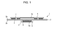
- Fig. 1 is a cross-sectional view of a printed circuit board according to a first embodiment.
- Fig. 2A and Fig. 2B are plan views of first and second semiconductor packages, respectively.
- Fig. 3A and Fig. 3B are plan views of first and second surfaces, respectively, of a printed wiring board according to the first embodiment.
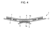
- Fig. 4 is a cross-sectional view illustrating a thermally deformed state of the printed circuit board according to the first embodiment.
- Fig. 5A and Fig. 5B are a cross-sectional view and a plan view, respectively, of a printed circuit board according to Comparative Example 1.
- Fig. 6A to Fig. 6D are cross-sectional views of printed circuit boards according to the related art.
- Fig. 1 is a cross-sectional view of a printed circuit board 1 according to the first embodiment.
- the printed circuit board 1 includes a printed wiring board 2, a first semiconductor package 4 mounted on a first surface 2a of the printed wiring board 2, and a second semiconductor package 6 mounted on a second surface 2b of the printed wiring board 2.
- the second surface 2b is on the back side of the first surface 2a.
- the first semiconductor package 4 includes a semiconductor device 4a mounted therein
- the second semiconductor package 6 includes a semiconductor device 6a mounted therein.
- the first semiconductor package 4 including the semiconductor device 4a is mounted on a first connection pad 3, with solder ball electrodes (first solder ball electrodes) 7 interposed therebetween.
- the first connection pad 3 is formed on the first surface 2a of the printed wiring board 2.
- the second semiconductor package 6 including the semiconductor device 6a is mounted on a second connection pad 5, with solder ball electrodes (second solder ball electrodes) 8 interposed therebetween.
- the second connection pad 5 is formed on the second surface 2b of the printed wiring board 2.
- Fig. 2A is a plan view of a lower surface of the first semiconductor package 4 (or surface facing the printed wiring board 2). As illustrated, the solder ball electrodes 7 are arranged on the first semiconductor package 4.
- Fig. 2B is a plan view of an upper surface of the second semiconductor package 6 (or surface facing the printed wiring board 2). As illustrated, the solder ball electrodes 8 are arranged on the second semiconductor package 6.
- Fig. 3A is a plan view of the first surface 2a of the printed wiring board 2 on which the first semiconductor package 4 is to be mounted.
- the first connection pad 3 on the first surface 2a is to be disposed on the solder ball electrodes 7 on the first semiconductor package 4.
- a region of the first surface 2a facing the first semiconductor package 4 includes a second region 10 in the center and a first region 9 around the second region 10.
- the second region 10 is a region where there is no first connection pad 3, whereas the first region 9 is a region where there is the first connection pad 3.
- Fig. 3B is a plan view of the second surface 2b of the printed wiring board 2 on which the second semiconductor package 6 is to be mounted.
- the second connection pad 5 on the second surface 2b is to be disposed on the solder ball electrodes 8 on the second semiconductor package 6.
- a region facing the second semiconductor package 6 is located within a region on the back side of the second region 10 where there is no first connection pad 3 illustrated in Fig. 3A .
- regions corresponding to the first region 9 and the second region 10 in Fig. 3A are indicated by respective dotted lines.
- the first region 9 is located around the second region 10.
- Fig. 4 is a cross-sectional view of the printed circuit board 1 deformed by heat generated by the semiconductor devices 4a and 6a mounted in the semiconductor packages 4 and 6.
- the printed wiring board 2 and the first semiconductor package 4 are expanded by heat generated by the semiconductor device 4a.
- the first semiconductor package 4 including the semiconductor device 4a made of silicon has a coefficient of linear expansion smaller than that of the printed wiring board 2 made of glass epoxy resin or the like. Therefore, the printed wiring board 2 and the first semiconductor package 4 have a tendency to warp such that they are raised at both ends.
- the printed wiring board 2 is provided with no solder ball electrodes 8 in an area opposite the solder ball electrodes 7. Therefore, as in the case of Fig. 6A described above, the printed wiring board 2 and the first semiconductor package 4 warp to be raised at both ends (or warp upward) as illustrated in Fig. 4 .
- the second semiconductor package 6 is expanded by heat generated by the semiconductor device 6a.
- the second semiconductor package 6 including the semiconductor device 6a made of silicon has a coefficient of linear expansion smaller than that of the printed wiring board 2. Therefore, the printed wiring board 2 and the second semiconductor package 6 have a tendency to warp such that they are lowered at both ends.
- the printed wiring board 2 is provided with no solder ball electrodes 7 in an area opposite the solder ball electrodes 8. Therefore, the printed wiring board 2 and the second semiconductor package 6 warp to be lowered at both ends (or warp downward) as illustrated in Fig. 4 .
- the printed wiring board 2 made of glass epoxy resin or the like is deformed more easily than the first semiconductor package 4 and the second semiconductor package 6, the printed wiring board 2 can be deformed in a complex manner as in Fig. 4 . That is, in the first region 9, which is an outer region of the printed wiring board 2, the printed wiring board 2 is deformed together with the first semiconductor package 4, whereas in the second region 10, which is an inner region of the printed wiring board 2, the printed wiring board 2 is deformed together with the second semiconductor package 6.
- the first region 9 where the first semiconductor package 4 is mounted and the second region 10 where the second semiconductor package 6 is mounted are two different regions. Therefore, although the semiconductor packages 4 and 6 are configured to warp in opposite directions, it is possible to fully release the stress applied to the solder ball electrodes 7 and 8 for joining the semiconductor packages 4 and 6, enhance the joint reliability, extend the joint life cycle, and realize high-density mounting.
- the first region 9 where the first semiconductor package 4 is mounted is located outside the second region 10 where the second semiconductor package 6 is mounted. That is, the first region 9 is located outside the second region 10 in the center of the printed wiring board 2.
- the present invention is not limited to this, and the second region 10 does not necessarily have to be located in the center inside the first region 9. However, if the second region 10 is located in the center inside the first region 9, the semiconductor packages 4 and 6 can be least affected by warping.
- the region facing the second semiconductor package 6 is located within the region on the back side of the second region 10 where there is no first connection pad 3 in the first surface 2a.
- the entire region facing the second semiconductor package 6 does not necessarily have to be located within the region on the back side of the second region 10. It is only necessary that at least the second connection pad 5 to be joined to the solder ball electrodes 8 for mounting the second semiconductor package 6 be located within the region on the back side of the second region 10.
- the printed wiring board 2 illustrated in Fig. 1 is used as a substrate in electronic apparatuses.
- the printed wiring board 2 is an eight-layer buildup substrate made of glass epoxy resin and measuring 110 mm x 50 mm in overall size and 0.8 mm in thickness.
- the first semiconductor package 4 (see Fig. 2A ) to be mounted on the printed wiring board 2 measures 13.0 mm x 13.0 mm in overall size and 1.3 mm in thickness.
- the solder ball electrodes 7 are arranged with a pitch of 0.5 mm and measure 0.3 mm in diameter.
- the total number of the solder ball electrodes 7 (or pins) is 320.
- This structure is generally referred to as a peripheral structure.
- the second semiconductor package 6 (see Fig. 2B ) to be mounted on the back side of the first semiconductor package 4 measures 5.5 mm x 5.5 mm in overall size and 1.1 mm in thickness.
- the solder ball electrodes 8 are arranged with a pitch of 0.5 mm and measure 0.3 mm in diameter.
- the second semiconductor package 6 is a small-sized semiconductor package where the total number of the solder ball electrodes 8 (or pins) is 64.
- the second semiconductor package 6 is mounted within a region facing the second region 10 of the printed wiring board 2. In other words, the second semiconductor package 6 is mounted such that the entire second connection pad 5 for connecting the second semiconductor package 6 is placed within the region facing the second region 10.
- a thermal stress test was performed to measure the durability of each solder ball electrode of the printed circuit board 1.
- One cycle of the thermal stress test involved placing the printed circuit board 1 inside a chamber, holding the printed circuit board 1 at -25°C for 9 minutes, heating the atmosphere to 125°C in 1 minute, holding the printed circuit board 1 again at 125°C for 9 minutes, and cooling the atmosphere to -25°C in 1 minute.
- the solder ball electrodes 8 at the corners of the second semiconductor package 6 were broken after 380 cycles. The detection of the breakage was determined when the resistance of each solder ball electrode measured online was increased 10% or more.
- Fig. 5A is a cross-sectional view of a printed circuit board 11 according to Comparative Example 1.
- the same components as those illustrated in Fig. 1 are given the same reference numerals.
- the first semiconductor package 4 is mounted on a first surface 12a of a printed wiring board 12
- the second semiconductor package 6 is mounted on a second surface 12b of the printed wiring board 12.
- the first semiconductor package 4 is mounted on the printed wiring board 12 with the first connection pad 3 and the solder ball electrodes 7 interposed therebetween.
- the second semiconductor package 6 is mounted on the printed wiring board 12 with the second connection pad 5 and the solder ball electrodes 8 interposed therebetween.
- the dimensions of the printed wiring board 12, the first semiconductor package 4, and the second semiconductor package 6 are the same as those in Example 1 described above.
- the first semiconductor package 4 includes the semiconductor device 4a mounted therein
- the second semiconductor package 6 includes the semiconductor device 6a mounted therein.
- Fig. 5B is a plan view illustrating an overlapping portion of the first connection pad 3 and the second connection pad 5 of the printed circuit board 11, as viewed through the first semiconductor package 4 from above.
- reference numeral 13 indicates an outline of the first semiconductor package 4
- reference numeral 14 indicates an outline of the second semiconductor package 6.
- the first connection pad 3 to which the solder ball electrodes 7 on the first semiconductor package 4 are joined and the second connection pad 5 to which the solder ball electrodes 8 on the second semiconductor package 6 are joined are disposed on the front and back sides, respectively, of the printed wiring board 12 such that they face each other.
- 56 out of 64 terminals of the second connection pad 5 coincide with the respective terminals of the first connection pad 3.
- the printed wiring board 12 is restrained from both the front and back sides in a region sandwiched between the solder ball electrodes 7 and 8. Therefore, since the printed wiring board 12 is unable to follow the expansion and warping of the semiconductor packages 4 and 6, the printed wiring board 12 is subjected to stress and degraded in durability.
- Example 1 The same thermal stress test as that in Example 1 was performed to measure the durability of each solder ball electrode of the printed circuit board 11. After 250 cycles of the thermal stress test on the printed circuit board 11, the solder ball electrodes 8 at the corners of the second semiconductor package 6 were broken.
- a region for mounting a first semiconductor package (4) is divided into a first region (9) on which first solder ball electrodes (7) are disposed and a second region (10) on which first solder ball electrodes are not disposed, and a region for mounting a second semiconductor package (6) on the back side of the first semiconductor package is located within a region on the back side of the second region.
Landscapes
- Engineering & Computer Science (AREA)
- Microelectronics & Electronic Packaging (AREA)
- Electric Connection Of Electric Components To Printed Circuits (AREA)
Abstract
Description
- The present invention relates to a printed circuit board in which semiconductor packages are mounted on a printed wiring board. In particular, the present invention relates to a printed circuit board in which semiconductor packages are mounted on front and back sides of a printed wiring board such that they face each other.
- Electronic apparatuses, such as mobile phones and video cameras, have been rapidly becoming smaller in recent years. A printed circuit board included in such electronic apparatuses and electronic components mounted on such a printed circuit board have been demanded to achieve both increased functionality and reduced size.
- To meet such demands, electronic components have been changed from those called quad flat packages (QFPs) with lead terminals therearound to those having a structure in which electrodes are arranged in a matrix on the back side to achieve higher pin count and reduced size. Some well-known examples of such electronic components include semiconductor packages called a ball grid array (BGA) and a chip size package (CSP). To meet demands for reduced size, such semiconductor packages are mounted on both sides of a printed wiring board in a printed circuit board to reduce the overall size of the electronic apparatus.
- However, turning on the electronic apparatus causes semiconductor devices included in the semiconductor packages to generate heat. The heat generated by the semiconductor devices causes expansion and deformation of the semiconductor packages and the printed wiring board having the semiconductor packages mounted thereon.
-
Fig. 6A illustrates a printed circuit board in which a semiconductor package is mounted only on one side of a printed wiring board. The printed circuit board illustrated inFig. 6A includes a printedwiring board 21, asemiconductor package 22 having a semiconductor device (not shown) mounted therein, andsolder ball electrodes 23 serving as connection terminals for joining the printedwiring board 21 to thesemiconductor package 22. In this case, heat generated by the semiconductor device mounted in thesemiconductor package 22 causes expansion of thesemiconductor package 22 and the printedwiring board 21. Due to a difference in coefficient of linear expansion between thesemiconductor package 22 and the printedwiring board 21, stress is applied to thesolder ball electrodes 23. Thesemiconductor package 22 and the printedwiring board 21 having thesemiconductor package 22 mounted thereon warp to reduce the stress applied to thesolder ball electrodes 23. - The coefficient of linear expansion of the
semiconductor package 22 in which the semiconductor device made of silicon is mounted is smaller than that of the printedwiring board 21 made of glass epoxy resin or the like. Therefore, as illustrated inFig. 6A , thesemiconductor package 22 and the printedwiring board 21 having thesemiconductor package 22 mounted thereon warp together to be raised at both ends (or warp upward). -
Fig. 6B is a cross-sectional view of a printed circuit board in which two identical semiconductor packages are mounted on both sides of a printed wiring board such that they face each other. The printed circuit board illustrated inFig. 6B includes a printedwiring board 24,semiconductor packages solder ball electrodes 27 for joining the printedwiring board 24 to both of thesemiconductor packages semiconductor packages semiconductor packages wiring board 24. Due to a difference in coefficient of linear expansion between thesemiconductor packages wiring board 24, stress is applied to thesolder ball electrodes 27. This causes thesemiconductor packages wiring board 24 is unable to warp. Therefore, the stress applied to thesolder ball electrodes 27 is not reduced and accumulates in thesolder ball electrodes 27. This significantly degrades the joint reliability of thesolder ball electrodes 27. - To improve the joint reliability of solder ball electrodes, Japanese Patent Laid-Open No.
2004-273617 Fig. 6C ,semiconductor packages wiring board 28 such that they partially face each other. - However, as the sizes of electronic apparatuses degrease, the frequencies of signals used in such electronic apparatuses increase. Therefore, it is desired to minimize the distance between the semiconductor packages mounted on the front and back sides of the printed wiring board. It is thus necessary to reduce the distance between the semiconductor packages on the front and back sides so as to reduce the length of wiring for connection between the semiconductor packages, thereby maintaining the quality of propagating signals. To maintain signal quality, it is necessary to provide a configuration in which the semiconductor packages are arranged on the front and back sides of the printed wiring board such that they do not face each other, or that they partially face each other as in the case of Japanese Patent Laid-Open No.
2004-273617 - In printed circuit boards, BGA semiconductor packages with much smaller sizes than before have been increasingly used in recent years. As compared to large-sized semiconductor packages, small-sized semiconductor packages are smaller in the diameter of solder ball electrodes, smaller in the area of connection pads, smaller in the number of solder ball electrodes, and thus lower in the strength of joining to the printed wiring board. Additionally, due to their thinner substrates, small-sized semiconductor packages are less rigid than large-sized semiconductor packages.
-
Fig. 6D illustrates a printed circuit board in which a small-sized semiconductor package and a normal-sized semiconductor package are mounted on both sides of a printed wiring board such that they face each other. The printed circuit board illustrated inFig. 6D includes a printedwiring board 31, asemiconductor package 32 having a semiconductor device (not shown) mounted therein,solder ball electrodes 33 serving as connection terminals for joining the printedwiring board 31 to thesemiconductor package 32, a small-sized semiconductor package 34 having a semiconductor device (not shown) mounted therein and a smaller number of connected terminals than thesemiconductor package 32, andsolder ball electrodes 35 serving as connection terminals for joining the printedwiring board 31 to the small-sized semiconductor package 34. As can be seen fromFig. 6D , the printedwiring board 31 warps to be raised at both ends (or warps upward), whereas the small-sized semiconductor package 34 warps to be lowered at both ends (or warps downward). This causes large stress to accumulate in thesolder ball electrodes 35. Therefore, when the small-sized semiconductor package 34 is mounted on the back side of the normal-sizedsemiconductor package 32 as illustrated inFig. 6D , the small-sized semiconductor package 34 suffers degraded joint reliability and short joint life cycle. - The present invention provides a high-density printed circuit board which allows semiconductor packages to be mounted on front and back sides of a printed wiring board such that they face each other, without causing degradation in joint life cycle of the semiconductor packages.
- The present invention in its first aspect provides a printed circuit board as specified in
claims 1 to 3. - Further features of the present invention will become apparent from the following description of exemplary embodiments with reference to the attached drawings.
-
Fig. 1 is a cross-sectional view of a printed circuit board according to a first embodiment. -
Fig. 2A and Fig. 2B are plan views of first and second semiconductor packages, respectively. -
Fig. 3A and Fig. 3B are plan views of first and second surfaces, respectively, of a printed wiring board according to the first embodiment. -
Fig. 4 is a cross-sectional view illustrating a thermally deformed state of the printed circuit board according to the first embodiment. -
Fig. 5A and Fig. 5B are a cross-sectional view and a plan view, respectively, of a printed circuit board according to Comparative Example 1. -
Fig. 6A to Fig. 6D are cross-sectional views of printed circuit boards according to the related art. - A first embodiment of the present invention will now be described with reference to
Fig. 1 to Fig. 4 . -
Fig. 1 is a cross-sectional view of a printedcircuit board 1 according to the first embodiment. The printedcircuit board 1 includes a printedwiring board 2, afirst semiconductor package 4 mounted on afirst surface 2a of the printedwiring board 2, and asecond semiconductor package 6 mounted on asecond surface 2b of the printedwiring board 2. Thesecond surface 2b is on the back side of thefirst surface 2a. Thefirst semiconductor package 4 includes asemiconductor device 4a mounted therein, and thesecond semiconductor package 6 includes asemiconductor device 6a mounted therein. - The
first semiconductor package 4 including thesemiconductor device 4a is mounted on afirst connection pad 3, with solder ball electrodes (first solder ball electrodes) 7 interposed therebetween. Thefirst connection pad 3 is formed on thefirst surface 2a of the printedwiring board 2. Similarly, thesecond semiconductor package 6 including thesemiconductor device 6a is mounted on asecond connection pad 5, with solder ball electrodes (second solder ball electrodes) 8 interposed therebetween. Thesecond connection pad 5 is formed on thesecond surface 2b of the printedwiring board 2. -
Fig. 2A is a plan view of a lower surface of the first semiconductor package 4 (or surface facing the printed wiring board 2). As illustrated, thesolder ball electrodes 7 are arranged on thefirst semiconductor package 4.Fig. 2B is a plan view of an upper surface of the second semiconductor package 6 (or surface facing the printed wiring board 2). As illustrated, thesolder ball electrodes 8 are arranged on thesecond semiconductor package 6. -
Fig. 3A is a plan view of thefirst surface 2a of the printedwiring board 2 on which thefirst semiconductor package 4 is to be mounted. Thefirst connection pad 3 on thefirst surface 2a is to be disposed on thesolder ball electrodes 7 on thefirst semiconductor package 4. As illustrated inFig. 3A , a region of thefirst surface 2a facing thefirst semiconductor package 4 includes asecond region 10 in the center and afirst region 9 around thesecond region 10. Thesecond region 10 is a region where there is nofirst connection pad 3, whereas thefirst region 9 is a region where there is thefirst connection pad 3. -
Fig. 3B is a plan view of thesecond surface 2b of the printedwiring board 2 on which thesecond semiconductor package 6 is to be mounted. Thesecond connection pad 5 on thesecond surface 2b is to be disposed on thesolder ball electrodes 8 on thesecond semiconductor package 6. InFig. 3B , a region facing thesecond semiconductor package 6 is located within a region on the back side of thesecond region 10 where there is nofirst connection pad 3 illustrated inFig. 3A . For ease of understanding, inFig. 3B , regions corresponding to thefirst region 9 and thesecond region 10 inFig. 3A are indicated by respective dotted lines. As can be seen fromFig. 3A , thefirst region 9 is located around thesecond region 10. -
Fig. 4 is a cross-sectional view of the printedcircuit board 1 deformed by heat generated by thesemiconductor devices semiconductor packages wiring board 2 and thefirst semiconductor package 4 are expanded by heat generated by thesemiconductor device 4a. Thefirst semiconductor package 4 including thesemiconductor device 4a made of silicon has a coefficient of linear expansion smaller than that of the printedwiring board 2 made of glass epoxy resin or the like. Therefore, the printedwiring board 2 and thefirst semiconductor package 4 have a tendency to warp such that they are raised at both ends. The printedwiring board 2 is provided with nosolder ball electrodes 8 in an area opposite thesolder ball electrodes 7. Therefore, as in the case ofFig. 6A described above, the printedwiring board 2 and thefirst semiconductor package 4 warp to be raised at both ends (or warp upward) as illustrated inFig. 4 . - At the same time, the
second semiconductor package 6 is expanded by heat generated by thesemiconductor device 6a. As in thefirst semiconductor package 4, thesecond semiconductor package 6 including thesemiconductor device 6a made of silicon has a coefficient of linear expansion smaller than that of the printedwiring board 2. Therefore, the printedwiring board 2 and thesecond semiconductor package 6 have a tendency to warp such that they are lowered at both ends. The printedwiring board 2 is provided with nosolder ball electrodes 7 in an area opposite thesolder ball electrodes 8. Therefore, the printedwiring board 2 and thesecond semiconductor package 6 warp to be lowered at both ends (or warp downward) as illustrated inFig. 4 . - Since the printed
wiring board 2 made of glass epoxy resin or the like is deformed more easily than thefirst semiconductor package 4 and thesecond semiconductor package 6, the printedwiring board 2 can be deformed in a complex manner as inFig. 4 . That is, in thefirst region 9, which is an outer region of the printedwiring board 2, the printedwiring board 2 is deformed together with thefirst semiconductor package 4, whereas in thesecond region 10, which is an inner region of the printedwiring board 2, the printedwiring board 2 is deformed together with thesecond semiconductor package 6. - In the present embodiment, the
first region 9 where thefirst semiconductor package 4 is mounted and thesecond region 10 where thesecond semiconductor package 6 is mounted are two different regions. Therefore, although thesemiconductor packages solder ball electrodes semiconductor packages - In the present embodiment, the
first region 9 where thefirst semiconductor package 4 is mounted is located outside thesecond region 10 where thesecond semiconductor package 6 is mounted. That is, thefirst region 9 is located outside thesecond region 10 in the center of the printedwiring board 2. The present invention is not limited to this, and thesecond region 10 does not necessarily have to be located in the center inside thefirst region 9. However, if thesecond region 10 is located in the center inside thefirst region 9, thesemiconductor packages - In the present embodiment, in the
second surface 2b of the printedwiring board 2 on which thesecond semiconductor package 6 is mounted, the region facing thesecond semiconductor package 6 is located within the region on the back side of thesecond region 10 where there is nofirst connection pad 3 in thefirst surface 2a. In the present invention, however, the entire region facing thesecond semiconductor package 6 does not necessarily have to be located within the region on the back side of thesecond region 10. It is only necessary that at least thesecond connection pad 5 to be joined to thesolder ball electrodes 8 for mounting thesecond semiconductor package 6 be located within the region on the back side of thesecond region 10. - Example 1 of the first embodiment will now be described.
- The printed
wiring board 2 illustrated inFig. 1 is used as a substrate in electronic apparatuses. Specifically, the printedwiring board 2 is an eight-layer buildup substrate made of glass epoxy resin and measuring 110 mm x 50 mm in overall size and 0.8 mm in thickness. - The first semiconductor package 4 (see
Fig. 2A ) to be mounted on the printedwiring board 2 measures 13.0 mm x 13.0 mm in overall size and 1.3 mm in thickness. Thesolder ball electrodes 7 are arranged with a pitch of 0.5 mm and measure 0.3 mm in diameter. The total number of the solder ball electrodes 7 (or pins) is 320. In the center of thefirst semiconductor package 4, there is a 6.0 mm x 6.0 mm region (corresponding to thesecond region 10 illustrated inFig. 3A and Fig. 3B ) where there are nosolder ball electrodes 7. This structure is generally referred to as a peripheral structure. - The second semiconductor package 6 (see
Fig. 2B ) to be mounted on the back side of thefirst semiconductor package 4 measures 5.5 mm x 5.5 mm in overall size and 1.1 mm in thickness. Thesolder ball electrodes 8 are arranged with a pitch of 0.5 mm and measure 0.3 mm in diameter. Thesecond semiconductor package 6 is a small-sized semiconductor package where the total number of the solder ball electrodes 8 (or pins) is 64. Thesecond semiconductor package 6 is mounted within a region facing thesecond region 10 of the printedwiring board 2. In other words, thesecond semiconductor package 6 is mounted such that the entiresecond connection pad 5 for connecting thesecond semiconductor package 6 is placed within the region facing thesecond region 10. - A thermal stress test was performed to measure the durability of each solder ball electrode of the printed
circuit board 1. One cycle of the thermal stress test involved placing the printedcircuit board 1 inside a chamber, holding the printedcircuit board 1 at -25°C for 9 minutes, heating the atmosphere to 125°C in 1 minute, holding the printedcircuit board 1 again at 125°C for 9 minutes, and cooling the atmosphere to -25°C in 1 minute. In the printedcircuit board 1 of Example 1, thesolder ball electrodes 8 at the corners of thesecond semiconductor package 6 were broken after 380 cycles. The detection of the breakage was determined when the resistance of each solder ball electrode measured online was increased 10% or more. - In thermal stress tests, printed circuit boards proven to withstand 260 to 310 cycles or more are generally determined to be non-defective. This means that the printed
circuit board 1 of Example 1 fully satisfied this requirement. The determination of a non-defective product in the thermal stress test was made by taking into account reported data ("Formula for predicting thermal fatigue life of lead-free solder" presented at the reporting session on environment-conscious advanced packaging technology in 2011) from Japan Electronics and Information Technology Industries Association (JEITA). -
Fig. 5A is a cross-sectional view of a printedcircuit board 11 according to Comparative Example 1. InFig. 5A , the same components as those illustrated inFig. 1 are given the same reference numerals. In the printedcircuit board 11, thefirst semiconductor package 4 is mounted on afirst surface 12a of a printedwiring board 12, and thesecond semiconductor package 6 is mounted on asecond surface 12b of the printedwiring board 12. Thefirst semiconductor package 4 is mounted on the printedwiring board 12 with thefirst connection pad 3 and thesolder ball electrodes 7 interposed therebetween. Similarly, thesecond semiconductor package 6 is mounted on the printedwiring board 12 with thesecond connection pad 5 and thesolder ball electrodes 8 interposed therebetween. In Comparative Example 1, the dimensions of the printedwiring board 12, thefirst semiconductor package 4, and thesecond semiconductor package 6 are the same as those in Example 1 described above. Again, thefirst semiconductor package 4 includes thesemiconductor device 4a mounted therein, and thesecond semiconductor package 6 includes thesemiconductor device 6a mounted therein. -
Fig. 5B is a plan view illustrating an overlapping portion of thefirst connection pad 3 and thesecond connection pad 5 of the printedcircuit board 11, as viewed through thefirst semiconductor package 4 from above. Note thatreference numeral 13 indicates an outline of thefirst semiconductor package 4, andreference numeral 14 indicates an outline of thesecond semiconductor package 6. Thefirst connection pad 3 to which thesolder ball electrodes 7 on thefirst semiconductor package 4 are joined and thesecond connection pad 5 to which thesolder ball electrodes 8 on thesecond semiconductor package 6 are joined are disposed on the front and back sides, respectively, of the printedwiring board 12 such that they face each other. As illustrated inFig. 5B , 56 out of 64 terminals of thesecond connection pad 5 coincide with the respective terminals of thefirst connection pad 3. - In Comparative Example 1, the printed
wiring board 12 is restrained from both the front and back sides in a region sandwiched between thesolder ball electrodes wiring board 12 is unable to follow the expansion and warping of thesemiconductor packages wiring board 12 is subjected to stress and degraded in durability. - The same thermal stress test as that in Example 1 was performed to measure the durability of each solder ball electrode of the printed
circuit board 11. After 250 cycles of the thermal stress test on the printedcircuit board 11, thesolder ball electrodes 8 at the corners of thesecond semiconductor package 6 were broken. - While the present invention has been described with reference to exemplary embodiments, it is to be understood that the invention is not limited to the disclosed exemplary embodiments. The scope of the following claims is to be accorded the broadest interpretation so as to encompass all such modifications and equivalent structures and functions. In a printed wiring board (2) of a printed circuit board, a region for mounting a first semiconductor package (4) is divided into a first region (9) on which first solder ball electrodes (7) are disposed and a second region (10) on which first solder ball electrodes are not disposed, and a region for mounting a second semiconductor package (6) on the back side of the first semiconductor package is located within a region on the back side of the second region.
Claims (3)
- A printed circuit board comprising:a printed wiring board (2);a first semiconductor package (4) mounted on a first surface (2a) of the printed wiring board with first solder ball electrodes (7) interposed therebetween; anda second semiconductor package (6) mounted on a second surface (2b) of the printed wiring board with second solder ball electrodes (8) interposed therebetween, the second surface being on the back side of the first surface, the second semiconductor package being smaller in size than the first semiconductor package,wherein a region of the printed wiring board on which the first semiconductor package is mounted, the region facing the first semiconductor package, includes a first region (9) on which the first solder ball electrodes are disposed and a second region (10) on which the first solder ball electrodes are not disposed; anda region of the printed wiring board on which the second semiconductor package is mounted, the region having the second solder ball electrodes formed thereon, is located within a region of the printed wiring board, the region being on the back side of the second region.
- The printed circuit board according to Claim 1, wherein a region of the printed wiring board on which the second semiconductor package is mounted, the region facing the second semiconductor package, is located within a region of the printed wiring board, the region being on the back side of the second region.
- The printed circuit board according to Claim 1 or 2, wherein the first region is located around the second region.
Applications Claiming Priority (1)
| Application Number | Priority Date | Filing Date | Title |
|---|---|---|---|
| JP2011246716A JP5893351B2 (en) | 2011-11-10 | 2011-11-10 | Printed circuit board |
Publications (1)
| Publication Number | Publication Date |
|---|---|
| EP2603063A1 true EP2603063A1 (en) | 2013-06-12 |
Family
ID=47143690
Family Applications (1)
| Application Number | Title | Priority Date | Filing Date |
|---|---|---|---|
| EP12191363.6A Withdrawn EP2603063A1 (en) | 2011-11-10 | 2012-11-06 | Printed circuit board |
Country Status (3)
| Country | Link |
|---|---|
| US (1) | US20130119541A1 (en) |
| EP (1) | EP2603063A1 (en) |
| JP (1) | JP5893351B2 (en) |
Families Citing this family (3)
| Publication number | Priority date | Publication date | Assignee | Title |
|---|---|---|---|---|
| JP2014229761A (en) * | 2013-05-23 | 2014-12-08 | 株式会社東芝 | Electronic apparatus |
| JP6230520B2 (en) * | 2014-10-29 | 2017-11-15 | キヤノン株式会社 | Printed circuit board and electronic device |
| JP6916471B2 (en) * | 2017-01-19 | 2021-08-11 | 株式会社村田製作所 | Electronic components and manufacturing methods for electronic components |
Citations (5)
| Publication number | Priority date | Publication date | Assignee | Title |
|---|---|---|---|---|
| JP2004273617A (en) | 2003-03-06 | 2004-09-30 | Canon Inc | Semiconductor device |
| US20070164445A1 (en) * | 2006-01-13 | 2007-07-19 | Nec Electronics Corporation | Substrate and semiconductor device |
| US20100037325A1 (en) * | 2004-11-15 | 2010-02-11 | Westerinen William J | Enhanced Packaging for PC Security |
| WO2011048862A1 (en) * | 2009-10-23 | 2011-04-28 | 株式会社フジクラ | Device-mounting structure and device-mounting method |
| US20110116247A1 (en) * | 2009-11-19 | 2011-05-19 | Samsung Electronics Co., Ltd | Semiconductor package having multi pitch ball land |
Family Cites Families (3)
| Publication number | Priority date | Publication date | Assignee | Title |
|---|---|---|---|---|
| JP4738996B2 (en) * | 2004-12-13 | 2011-08-03 | キヤノン株式会社 | Semiconductor device |
| US8643163B2 (en) * | 2005-08-08 | 2014-02-04 | Stats Chippac Ltd. | Integrated circuit package-on-package stacking system and method of manufacture thereof |
| US20090039490A1 (en) * | 2007-08-08 | 2009-02-12 | Powertech Technology Inc. | Mounting assembly of semiconductor packages prevent soldering defects caused by substrate warpage |
-
2011
- 2011-11-10 JP JP2011246716A patent/JP5893351B2/en not_active Expired - Fee Related
-
2012
- 2012-11-06 US US13/670,202 patent/US20130119541A1/en not_active Abandoned
- 2012-11-06 EP EP12191363.6A patent/EP2603063A1/en not_active Withdrawn
Patent Citations (6)
| Publication number | Priority date | Publication date | Assignee | Title |
|---|---|---|---|---|
| JP2004273617A (en) | 2003-03-06 | 2004-09-30 | Canon Inc | Semiconductor device |
| US20100037325A1 (en) * | 2004-11-15 | 2010-02-11 | Westerinen William J | Enhanced Packaging for PC Security |
| US20070164445A1 (en) * | 2006-01-13 | 2007-07-19 | Nec Electronics Corporation | Substrate and semiconductor device |
| WO2011048862A1 (en) * | 2009-10-23 | 2011-04-28 | 株式会社フジクラ | Device-mounting structure and device-mounting method |
| EP2493273A1 (en) * | 2009-10-23 | 2012-08-29 | Fujikura, Ltd. | Device-mounting structure and device-mounting method |
| US20110116247A1 (en) * | 2009-11-19 | 2011-05-19 | Samsung Electronics Co., Ltd | Semiconductor package having multi pitch ball land |
Also Published As
| Publication number | Publication date |
|---|---|
| US20130119541A1 (en) | 2013-05-16 |
| JP5893351B2 (en) | 2016-03-23 |
| JP2013105785A (en) | 2013-05-30 |
Similar Documents
| Publication | Publication Date | Title |
|---|---|---|
| US9082645B2 (en) | Manufacturing method of semiconductor module | |
| JP4512545B2 (en) | Multilayer semiconductor module | |
| JP4473807B2 (en) | Multilayer semiconductor device and lower layer module of multilayer semiconductor device | |
| CN101647109B (en) | Semiconductor device | |
| US8508031B2 (en) | Electronic device and method of producing the same | |
| JP2006502587A (en) | Components, methods and assemblies for multichip packages | |
| CN101960591A (en) | Semiconductor device, semiconductor device manufacturing method, printed circuit board and electronic device | |
| JP5092054B2 (en) | Mounting board and failure prediction method | |
| CN1983581A (en) | Semiconductor device | |
| CN101546743B (en) | Mounting structure of semiconductor device and electronic apparatus using same | |
| JP2014063844A (en) | Semiconductor device, semiconductor device manufacturing method and electronic apparatus | |
| EP2603063A1 (en) | Printed circuit board | |
| CN101546742B (en) | Mounting structure of semiconductor device and electronic equipment using the mounting structure | |
| KR100642356B1 (en) | Semiconductor device and mu1ti1ayer substrate therefor | |
| US9601470B2 (en) | Stacked semiconductor device, printed circuit board, and method for manufacturing stacked semiconductor device | |
| US8344521B2 (en) | Semiconductor device, semiconductor package and wiring structure | |
| JP5361134B2 (en) | Pressure head and component crimping device | |
| JP5017881B2 (en) | Semiconductor device | |
| JP2000150775A (en) | Semiconductor element mounting jig and semiconductor element mounting method | |
| JP2001320145A (en) | Method and structure for mounting electronic part | |
| JP2020072143A (en) | Electronic device | |
| JP2007317754A (en) | Semiconductor device | |
| US20050029011A1 (en) | Circuit board | |
| JP2007305652A (en) | Semiconductor package | |
| JP2002110860A (en) | Resin-bonded double-sided metal structure |
Legal Events
| Date | Code | Title | Description |
|---|---|---|---|
| PUAI | Public reference made under article 153(3) epc to a published international application that has entered the european phase |
Free format text: ORIGINAL CODE: 0009012 |
|
| AK | Designated contracting states |
Kind code of ref document: A1 Designated state(s): AL AT BE BG CH CY CZ DE DK EE ES FI FR GB GR HR HU IE IS IT LI LT LU LV MC MK MT NL NO PL PT RO RS SE SI SK SM TR |
|
| AX | Request for extension of the european patent |
Extension state: BA ME |
|
| 17P | Request for examination filed |
Effective date: 20131212 |
|
| RBV | Designated contracting states (corrected) |
Designated state(s): AL AT BE BG CH CY CZ DE DK EE ES FI FR GB GR HR HU IE IS IT LI LT LU LV MC MK MT NL NO PL PT RO RS SE SI SK SM TR |
|
| 17Q | First examination report despatched |
Effective date: 20140613 |
|
| STAA | Information on the status of an ep patent application or granted ep patent |
Free format text: STATUS: THE APPLICATION HAS BEEN WITHDRAWN |
|
| 18W | Application withdrawn |
Effective date: 20151221 |