EP2602812A1 - High-quality gan high-voltage hfets on silicon - Google Patents
High-quality gan high-voltage hfets on silicon Download PDFInfo
- Publication number
- EP2602812A1 EP2602812A1 EP20120193443 EP12193443A EP2602812A1 EP 2602812 A1 EP2602812 A1 EP 2602812A1 EP 20120193443 EP20120193443 EP 20120193443 EP 12193443 A EP12193443 A EP 12193443A EP 2602812 A1 EP2602812 A1 EP 2602812A1
- Authority
- EP
- European Patent Office
- Prior art keywords
- film
- gan
- voids
- laminate
- silicon
- Prior art date
- Legal status (The legal status is an assumption and is not a legal conclusion. Google has not performed a legal analysis and makes no representation as to the accuracy of the status listed.)
- Granted
Links
Images



Classifications
-
- H—ELECTRICITY
- H10—SEMICONDUCTOR DEVICES; ELECTRIC SOLID-STATE DEVICES NOT OTHERWISE PROVIDED FOR
- H10D—INORGANIC ELECTRIC SEMICONDUCTOR DEVICES
- H10D62/00—Semiconductor bodies, or regions thereof, of devices having potential barriers
- H10D62/80—Semiconductor bodies, or regions thereof, of devices having potential barriers characterised by the materials
- H10D62/82—Heterojunctions
- H10D62/824—Heterojunctions comprising only Group III-V materials heterojunctions, e.g. GaN/AlGaN heterojunctions
-
- H—ELECTRICITY
- H10—SEMICONDUCTOR DEVICES; ELECTRIC SOLID-STATE DEVICES NOT OTHERWISE PROVIDED FOR
- H10D—INORGANIC ELECTRIC SEMICONDUCTOR DEVICES
- H10D30/00—Field-effect transistors [FET]
- H10D30/40—FETs having zero-dimensional [0D], one-dimensional [1D] or two-dimensional [2D] charge carrier gas channels
- H10D30/47—FETs having zero-dimensional [0D], one-dimensional [1D] or two-dimensional [2D] charge carrier gas channels having two-dimensional [2D] charge carrier gas channels, e.g. nanoribbon FETs or high electron mobility transistors [HEMT]
-
- H—ELECTRICITY
- H10—SEMICONDUCTOR DEVICES; ELECTRIC SOLID-STATE DEVICES NOT OTHERWISE PROVIDED FOR
- H10D—INORGANIC ELECTRIC SEMICONDUCTOR DEVICES
- H10D30/00—Field-effect transistors [FET]
- H10D30/60—Insulated-gate field-effect transistors [IGFET]
-
- H—ELECTRICITY
- H10—SEMICONDUCTOR DEVICES; ELECTRIC SOLID-STATE DEVICES NOT OTHERWISE PROVIDED FOR
- H10D—INORGANIC ELECTRIC SEMICONDUCTOR DEVICES
- H10D62/00—Semiconductor bodies, or regions thereof, of devices having potential barriers
- H10D62/10—Shapes, relative sizes or dispositions of the regions of the semiconductor bodies; Shapes of the semiconductor bodies
- H10D62/17—Semiconductor regions connected to electrodes not carrying current to be rectified, amplified or switched, e.g. channel regions
- H10D62/351—Substrate regions of field-effect devices
- H10D62/357—Substrate regions of field-effect devices of FETs
-
- H—ELECTRICITY
- H10—SEMICONDUCTOR DEVICES; ELECTRIC SOLID-STATE DEVICES NOT OTHERWISE PROVIDED FOR
- H10D—INORGANIC ELECTRIC SEMICONDUCTOR DEVICES
- H10D62/00—Semiconductor bodies, or regions thereof, of devices having potential barriers
- H10D62/40—Crystalline structures
- H10D62/405—Orientations of crystalline planes
-
- H—ELECTRICITY
- H10—SEMICONDUCTOR DEVICES; ELECTRIC SOLID-STATE DEVICES NOT OTHERWISE PROVIDED FOR
- H10P—GENERIC PROCESSES OR APPARATUS FOR THE MANUFACTURE OR TREATMENT OF DEVICES COVERED BY CLASS H10
- H10P14/00—Formation of materials, e.g. in the shape of layers or pillars
- H10P14/20—Formation of materials, e.g. in the shape of layers or pillars of semiconductor materials
- H10P14/24—Formation of materials, e.g. in the shape of layers or pillars of semiconductor materials using chemical vapour deposition [CVD]
-
- H—ELECTRICITY
- H10—SEMICONDUCTOR DEVICES; ELECTRIC SOLID-STATE DEVICES NOT OTHERWISE PROVIDED FOR
- H10P—GENERIC PROCESSES OR APPARATUS FOR THE MANUFACTURE OR TREATMENT OF DEVICES COVERED BY CLASS H10
- H10P14/00—Formation of materials, e.g. in the shape of layers or pillars
- H10P14/20—Formation of materials, e.g. in the shape of layers or pillars of semiconductor materials
- H10P14/27—Formation of materials, e.g. in the shape of layers or pillars of semiconductor materials using selective deposition, e.g. simultaneous growth of monocrystalline and non-monocrystalline semiconductor materials
- H10P14/271—Formation of materials, e.g. in the shape of layers or pillars of semiconductor materials using selective deposition, e.g. simultaneous growth of monocrystalline and non-monocrystalline semiconductor materials characterised by the preparation of substrate for selective deposition
- H10P14/272—Formation of materials, e.g. in the shape of layers or pillars of semiconductor materials using selective deposition, e.g. simultaneous growth of monocrystalline and non-monocrystalline semiconductor materials characterised by the preparation of substrate for selective deposition using mask materials other than SiO2 or SiN
-
- H—ELECTRICITY
- H10—SEMICONDUCTOR DEVICES; ELECTRIC SOLID-STATE DEVICES NOT OTHERWISE PROVIDED FOR
- H10P—GENERIC PROCESSES OR APPARATUS FOR THE MANUFACTURE OR TREATMENT OF DEVICES COVERED BY CLASS H10
- H10P14/00—Formation of materials, e.g. in the shape of layers or pillars
- H10P14/20—Formation of materials, e.g. in the shape of layers or pillars of semiconductor materials
- H10P14/29—Formation of materials, e.g. in the shape of layers or pillars of semiconductor materials characterised by the substrates
- H10P14/2901—Materials
- H10P14/2902—Materials being Group IVA materials
- H10P14/2905—Silicon, silicon germanium or germanium
-
- H—ELECTRICITY
- H10—SEMICONDUCTOR DEVICES; ELECTRIC SOLID-STATE DEVICES NOT OTHERWISE PROVIDED FOR
- H10P—GENERIC PROCESSES OR APPARATUS FOR THE MANUFACTURE OR TREATMENT OF DEVICES COVERED BY CLASS H10
- H10P14/00—Formation of materials, e.g. in the shape of layers or pillars
- H10P14/20—Formation of materials, e.g. in the shape of layers or pillars of semiconductor materials
- H10P14/32—Formation of materials, e.g. in the shape of layers or pillars of semiconductor materials characterised by intermediate layers between substrates and deposited layers
- H10P14/3202—Materials thereof
- H10P14/3214—Materials thereof being Group IIIA-VA semiconductors
- H10P14/3216—Nitrides
-
- H—ELECTRICITY
- H10—SEMICONDUCTOR DEVICES; ELECTRIC SOLID-STATE DEVICES NOT OTHERWISE PROVIDED FOR
- H10P—GENERIC PROCESSES OR APPARATUS FOR THE MANUFACTURE OR TREATMENT OF DEVICES COVERED BY CLASS H10
- H10P14/00—Formation of materials, e.g. in the shape of layers or pillars
- H10P14/20—Formation of materials, e.g. in the shape of layers or pillars of semiconductor materials
- H10P14/32—Formation of materials, e.g. in the shape of layers or pillars of semiconductor materials characterised by intermediate layers between substrates and deposited layers
- H10P14/3202—Materials thereof
- H10P14/3238—Materials thereof being insulating materials
-
- H—ELECTRICITY
- H10—SEMICONDUCTOR DEVICES; ELECTRIC SOLID-STATE DEVICES NOT OTHERWISE PROVIDED FOR
- H10P—GENERIC PROCESSES OR APPARATUS FOR THE MANUFACTURE OR TREATMENT OF DEVICES COVERED BY CLASS H10
- H10P14/00—Formation of materials, e.g. in the shape of layers or pillars
- H10P14/20—Formation of materials, e.g. in the shape of layers or pillars of semiconductor materials
- H10P14/34—Deposited materials, e.g. layers
- H10P14/3402—Deposited materials, e.g. layers characterised by the chemical composition
- H10P14/3414—Deposited materials, e.g. layers characterised by the chemical composition being group IIIA-VIA materials
- H10P14/3416—Nitrides
-
- H—ELECTRICITY
- H10—SEMICONDUCTOR DEVICES; ELECTRIC SOLID-STATE DEVICES NOT OTHERWISE PROVIDED FOR
- H10P—GENERIC PROCESSES OR APPARATUS FOR THE MANUFACTURE OR TREATMENT OF DEVICES COVERED BY CLASS H10
- H10P14/00—Formation of materials, e.g. in the shape of layers or pillars
- H10P14/60—Formation of materials, e.g. in the shape of layers or pillars of insulating materials
- H10P14/63—Formation of materials, e.g. in the shape of layers or pillars of insulating materials characterised by the formation processes
- H10P14/6326—Deposition processes
-
- H—ELECTRICITY
- H10—SEMICONDUCTOR DEVICES; ELECTRIC SOLID-STATE DEVICES NOT OTHERWISE PROVIDED FOR
- H10D—INORGANIC ELECTRIC SEMICONDUCTOR DEVICES
- H10D30/00—Field-effect transistors [FET]
- H10D30/40—FETs having zero-dimensional [0D], one-dimensional [1D] or two-dimensional [2D] charge carrier gas channels
- H10D30/47—FETs having zero-dimensional [0D], one-dimensional [1D] or two-dimensional [2D] charge carrier gas channels having two-dimensional [2D] charge carrier gas channels, e.g. nanoribbon FETs or high electron mobility transistors [HEMT]
- H10D30/471—High electron mobility transistors [HEMT] or high hole mobility transistors [HHMT]
- H10D30/475—High electron mobility transistors [HEMT] or high hole mobility transistors [HHMT] having wider bandgap layer formed on top of lower bandgap active layer, e.g. undoped barrier HEMTs such as i-AlGaN/GaN HEMTs
-
- H—ELECTRICITY
- H10—SEMICONDUCTOR DEVICES; ELECTRIC SOLID-STATE DEVICES NOT OTHERWISE PROVIDED FOR
- H10D—INORGANIC ELECTRIC SEMICONDUCTOR DEVICES
- H10D62/00—Semiconductor bodies, or regions thereof, of devices having potential barriers
- H10D62/80—Semiconductor bodies, or regions thereof, of devices having potential barriers characterised by the materials
- H10D62/85—Semiconductor bodies, or regions thereof, of devices having potential barriers characterised by the materials being Group III-V materials, e.g. GaAs
- H10D62/8503—Nitride Group III-V materials, e.g. AlN or GaN
Definitions
- the present disclosure relates generally to gallium nitride (GaN) substrates, and, more specifically, the present disclosure relates to a method for fabricating a GaN substrate on silicon.
- GaN gallium nitride
- Wide-bandgap semiconductors are widely used for fabricating active devices for high-voltage applications.
- One type of semiconductor structure known as a heterostructure field effect transistors (HFET) also called high-electron mobility transistors (HEMT)
- HFET heterostructure field effect transistors
- HEMT high-electron mobility transistors
- wide-bandgap HFET devices may be used as a switching element in high-voltage switching power converters.
- GaN is one example of a wide-bandgap semiconductor that has generated particular interest.
- AlGaN/GaN HFETs show promise for power electronics due to their wider bandgap and high-electron saturation velocity, both of which enable high-voltage operation.
- the difficulty and expense in forming GaN substrates have limited the application of GaN-based devices to specific markets.
- a GaN substrate is typically manufactured by growing GaN film on another substrate, due to the expense and difficulty of manufacturing bulk GaN wafers.
- silicon carbide (SiC) or sapphire (Al 2 O 3 ) wafers may be used as handle wafers for a GaN substrate (i.e., a GaN film is deposited over the handle wafer).
- SiC silicon carbide
- sapphire Al 2 O 3
- sapphire is a poor thermal conductor and can present difficulties during packaging, and SiC wafers are still very expensive.
- both types of wafers are only available as smaller-diameter wafers, which eliminate the economy of scales available with larger diameters.
- GaN substrates Another option for creating GaN substrates is using a silicon handle wafer, which is inexpensive and available in large diameters. Additionally, backend grinding and lapping needed for packaging is well developed for silicon wafers. However, due to a large lattice mismatch and large thermal mismatch between GaN and silicon, it may be difficult to reliably grow GaN directly on a silicon (Si) substrate. Instead, the epitaxial growth of crack-free GaN on silicon may require extensive buffer layer engineering to minimize the bow and warp during and after growth. In addition, high-voltage applications (e.g., above 600 V) may require buffer layers in excess of 2.5 ⁇ m and even up to 4 ⁇ m (e.g., for 1,000 V applications).
- Si silicon
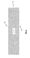
- FIG. 1 illustrates an example silicon wafer with exposed surfaces along the ⁇ 111> crystal orientation for use in fabricating a GaN substrate in accordance with an embodiment of the present invention.
- FIG. 2 illustrates a substrate at a stage of fabrication of a GaN substrate with a film of crystalline aluminum oxide Al 2 O 3 on the top surface of the wafer in accordance with an embodiment of the present invention.
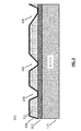
- FIG. 3 illustrates a substrate at another stage of fabrication of a GaN substrate with an amorphous film under the Al 2 O 3 film in accordance with an embodiment of the present invention.
- FIG. 4 illustrates a substrate at yet another stage of fabrication of a GaN substrate after a GaN film has been grown on top of an AlN film in accordance with an embodiment of the present invention.
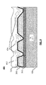
- FIG. 5 illustrates a substrate at still another stage of fabrication of a GaN substrate after several more interleaved layers of GaN and AlN films have been grown to form a surface suitable for HFET formation in accordance with an embodiment of the present invention.
- FIG. 6 is a flowchart for an example process of fabricating a GaN substrate that may be suitable for forming transistors and other devices in accordance with an embodiment of the present invention.
- FIGS. 1-5 illustrate a GaN substrate at various stages of an example process illustrated in FIG. 6 for creating a GaN substrate that may be suitable for use in fabricating transistors, such as HFETs.
- the blocks of flowchart 600 ( FIG. 6 ) are explained below with respect to FIGS. 1-5 and several example processing operations and steps.
- the features, shapes, and proportions of the substrate and structures shown in FIGS. 1-5 are not limiting on the claims. Additionally, it should be understood that the explanation below is for one example and is not limiting on the claims.
- a wafer 100 includes a top surface 104 and a bottom surface 102.
- wafer 100 is a ⁇ 111> silicon wafer.
- wafer 100 is a ⁇ 111> silicon wafer because top surface 104 and bottom surface 102 expose the ⁇ 111> crystal orientation of the crystalline silicon that forms the wafer.
- wafer 100 may be used as a handle wafer to grow a GaN film (not shown).
- a GaN film (not shown) may be grown over top surface 104 of wafer 100 or an intermediary layer.
- Wafer 100 may be a typical thickness, for example, between 500 ⁇ m and 1,000 ⁇ m, although other thicknesses may also be used.
- an aluminum oxide (Al 2 O 3 ) film 202 interfaces with top layer 104 of wafer 100.
- Al 2 O 3 film 202 provides a surface that is similar to the surface of a sapphire substrate, which may allow for reuse of processes developed for sapphire substrates.
- Al 2 O 3 film 202 may also act as a seed layer for subsequent film growth.
- Al 2 O 3 film 202 may be a seed layer for a subsequent aluminum nitride (AlN) film.
- Al 2 O 3 film 202 may have a c-axis orientation, which matches the ⁇ 111> surface of the silicon wafer (both are hexagonal).
- Crystalline Al 2 O 3 film 202 may be from 5 nm to 50 nm. In one example crystalline Al 2 O 3 film 202 is about 5 nm.
- FIG. 2 illustrates wafer 100 after crystalline Al 2 O 3 film 202 is grown over top surface 104 ( FIG. 1 ) of wafer 100.
- Al 2 O 3 film 202 is grown using a molecular beam epitaxy (MBE) tool and MBE process so that Al 2 O 3 film 202 is directly on the surface of wafer 100.
- MBE molecular beam epitaxy
- MBE allows deposition at lower temperatures, which may prevent oxidation of the silicon.
- Higher levels of vacuum while depositing Al 2 O 3 film 202 may also help prevent oxidation of the silicon.
- Other tools and processes, such as chemical vapor deposition (CVD) processes and tools may also be used to form Al 2 O 3 film 202 (with or without an intervening layer between Al 2 O 3 film 202 and the silicon surface of wafer 100).
- CVD chemical vapor deposition
- wafer 100 may exert a tensile stress on Al 2 O 3 film 202. Dislocations formed in Al 2 O 3 film 202 may relax the initial tensile stress and reduce warping. As will be described further below, additional GaN film layers may be grown on top of Al 2 O 3 film 202, which may allow a compressive stress to be exerted on Al 2 O 3 film 202 and contribute to alleviating the initial tensile stress and to limiting warp in wafer 100.
- crystalline Al 2 O 3 film 202 may be in direct contact with wafer 100, i.e., there are no intervening films between the top surface 104 of wafer 100 and Al 2 O 3 film 202. This may be the case if, for example, Al 2 O 3 film 202 was deposited in a manner that prevents oxidation of the surface of wafer 100 prior to formation of crystalline Al 2 O 3 film 202.
- semiconductor device 200 may be processed in a particular manner to allow an intermediate film (not shown) be formed between silicon wafer 100 and Al 2 O 3 film 202 to alleviate stress or for another purpose. For example, a layer of silicon aluminum oxide may be formed to relieve stress where wafer 100 interfaces with crystalline Al 2 O 3 film 202.
- amorphous film 302 is formed between wafer 100 and Al 2 O 3 film 304 in accordance with of embodiments of the present invention.
- amorphous film 302 is includes aluminum, silicon, and oxygen (AlSiO) from wafer 100 and Al 2 O 3 film.
- AlSiO oxygen
- voids 306 may form and change the surface topology of Al 2 O 3 film 202 as originally grown to form Al 2 O 3 film 304. Specifically, voids 306 may allow for reducing the density of dislocation through an annihilation process.
- voids 306 may expose amorphous AlSiO film 302; however, not all voids must expose amorphous AlSiO film 302. Additionally, AlN film 308 has been formed over Al 2 O 3 film 304 and exposed portions of amorphous film 302. In other examples, amorphous film 302 may be formed without voids. Also, in some cases AlN film 308 may not be formed on portions of amorphous film 302 that are exposed at the bottom of voids 306.
- amorphous film 302 may form between Al 2 O 3 film 304 and wafer 100 during a high-temperature anneal that may also cause Al 2 O 3 film 304 to pool and form voids 306 that may expose portions of amorphous film 302.
- Voids 306 may be filled in by subsequent film depositions and/or later overgrowth on the surface of Al 2 O 3 film 304 and may promote threading dislocation annihilation in later-formed GaN films by causing threading dislocations to curl back into other threading dislocations.
- voids 306 may also divert dislocations from traveling up to the substrate surface where fracture may occur. Even though voids 306 form in Al 2 O 3 film 304, regions of Al 2 O 3 film 304 may still maintain crystalline structure.
- amorphous film 302 may relieve the stress between Al 2 O 3 film 304 and wafer 100.
- the thickness of amorphous film 302 may be controlled by the temperature of wafer 100 and time at which wafer 100 is held at that temperature. In one example, amorphous film 302 may start to form at temperatures as low as 800° C. Typical thicknesses of amorphous film 302 are 2 nm to 10 nm. In one case, amorphous film 302 is 2 nm thick.
- void 306 and the AlSiO amorphous film 302 are formed during the process to grow an initial AlN film 308 on Al 2 O 3 film 304 in a metal organic chemical vaport deposition (MOCVD) tool.
- the first step of growing AlN film 308 may be a high-temperature anneal that removes contamination from the surface of Al 2 O 3 film 304 prior to growing AlN film 308.
- this high-temperature anneal may be about 850° C to 950° C for 5 to 20 minutes.
- voids 306 and amorphous film 302 may form.
- An example recipe for creating AlN film 308 starts with a nitridation process to form a thin AlN film on Al 2 O 3 film 308. Then, a low-temperature AlN film may be formed using (ammonia) NH 3 as a nitrogen source and trimethylaluminum (TMA) as an aluminum source in an MOCVD chamber.
- TMA trimethylaluminum
- the TMA provides aluminum that nucleates at the surface with nitrogen from the NH 3 to form an AlN film at a temperature of about 550° C to 650° C.
- the temperature may be raised as high as 1050° C for about 1 to 5 minutes to crystallize AlN.
- AlN film 308 may be, for example, about 20 nm thick, but the thickness may also be between 10 nm and 200 nm.
- FIG. 4 illustrates a substrate 400 after a stage during the fabrication of a GaN substrate.
- a first laminate layer has been formed, which includes AlN film 308 discussed above with respect to FIG. 3 and GaN film 402.
- the voids from Al 2 O 3 film 304 are still present in the surface of GaN film 402.
- the sizes of the voids have been significantly reduced.
- threading dislocations 404 can be seen in GaN film 402, particularly in the regions above the voids in Al 2 O 3 film 304.
- the AlN film may be grown over the Al 2 O 3 film and exposed amorphous film if the AlN film is part of the first laminate layer.
- Subsequent laminate layers may have an AlN film grown over a GaN film of the preceding laminate layer.
- the AlN film may be grown as described above with respect to block 604. Alternatively, other processes with different temperatures, growth rates, and V/III ratios may be used.
- the first laminate layer (where the AlN film is formed on the Al 2 O 3 film and exposed amorphous film) includes an AlN film that may be formed with a high-temperature process, but subsequent layers of AlN film used in subsequent laminate layers may use a process recipe that uses a lower peak temperature than the recipe used for the AlN film of the first laminate layer.
- the recipe for later-grown AlN films may omit the crystallization or nitridation steps.
- the AlN film of each laminate layer may be, for example, about 20 nm thick, but thickness may also be between 10 nm and 200 nm.
- a GaN film is grown over the AlN film.
- an MOCVD tool may be used to grow the GaN film.
- One example recipe may include a temperature of 1030° C, a pressure of 100 Torrs, and a V/III ratio (e.g., ratio of NH 3 to trimethylgallium (TMGA)) of about 2000, and a growth rate of 2 ⁇ m/hr.
- the same MOCVD chamber used for growing the AlN film may be used for the GaN film without removing the wafer from the tool.
- separate tools may be used for the AlN film and the GaN film.
- the GaN film in each of the plurality of laminate layers may be from 500 nm to 50,000 nm thick.
- the last GaN film may be several microns thick to support high-voltage (e.g., above 600 V) devices.
- the GaN film of the first laminate layer will not grow as a perfect crystal. Instead, this GaN film will have a relatively high density of defects, such as dislocations, and in particular, threading dislocations. Regions in the GaN film over a void in the Al 2 O 3 may have a particularly high threading dislocation density.
- a transistor such as an AlGaN/GaN HFET may be formed in the GaN film of the top laminate layer.
- This top GaN film may have a thickness that is suitable for the particular type of device to be formed.
- a top GaN film thickness of at least 2.5 ⁇ m may be desired. If even higher-voltage (e.g., 1000 V) devices are to be formed, a top GaN film thickness of 4 ⁇ m may be required.
- FIG. 5 illustrates a substrate 500 after another stage during the fabrication of a GaN substrate.
- Three additional laminate layers have been grown. Specifically, a laminate layer of AlN film 502 and GaN film 504, a laminate layer of AlN film 506 and GaN film 508, and a laminate layer of AlN film 510 and GaN film 512 have been grown. As can be seen, the threading dislocation density decreases in the GaN film for each subsequent laminate layer. Similarly, the voids from Al 2 O 3 film 302 shrink with each additional laminate layer.
- Top surface 514 of GaN film 512 may be suitable for forming a transistor (or other device), such as an AlGaN/GaN HFET.
- a transistor such as an AlGaN/GaN HFET may be formed in the GaN film of the top laminate layer.
- This top GaN film may have a thickness that is suitable for the particular type of device to be formed. For example, if high-voltage (e.g., above 600 V) devices are to be formed, a top GaN film thickness of at least 2.5 ⁇ m may be desired. If even higher-voltage (e.g., 1000 V) devices are to be formed, a top GaN film thickness of 4 ⁇ m may be required.
- GaN film 512 is illustrated without any threading dislocations, this represents that GaN film 512 has an improved threading dislocation density as compared to some or all of the previous laminate layers.
- one or more of the voids may still be present on the surface of the GaN film.
- the regions over the voids may have high rates of threading dislocation annihilation, even after just a second laminate layer.
- the GaN film of each laminate layer may have a lower threading dislocation density than the GaN film of the previous laminate layer. Accordingly, after some number of laminate layers, the GaN film may be flat (the voids are not visible on the surface) and the threading dislocation density may be at an acceptable level.
- some dislocation lines may be redirected from traveling up vertically to the surface and forming cracks.
- the new buffer layer described above may act like a sapphire substrate allowing easy transfer of epitaxial processes developed on sapphire.
- the buffer allows for a GaN substrate that may be less expensive than using sapphire substrates.
- the growth of GaN films on Al 2 O 3 may also be under continuous compressive stress (unlike when GaN is grown directly on silicon, where the GaN film can be either tensile or compressive, depending on the combination of layers used for stress engineering).
- the compressive stress of the GaN may compensate for the tensile stress generated by the thermal mismatch between silicon and GaN during cool-down of the substrate. This compensation may lead to crack-free GaN film, a thicker GaN film for high-voltage applications, and simplified transfer to 6-inch or 8-inch silicon substrates.
- Fig. 6 shows flow chart 600 for an example process of creating a GaN substrate.
- a ⁇ 111> silicon wafer is obtained with an Al 2 O 3 film on a top surface.
- an amorphous layer is formed at the interface between the Si wafer and Al 2 O 3 .
- voids are formed in the Al 2 O 3 film using, for example, a high-temperature anneal.
- a plurality of laminate layers are formed. Each laminate layer includes a GaN film on top of an AlN film.
Landscapes
- Recrystallisation Techniques (AREA)
- Junction Field-Effect Transistors (AREA)
- Chemical Vapour Deposition (AREA)
Abstract
Description
- The present disclosure relates generally to gallium nitride (GaN) substrates, and, more specifically, the present disclosure relates to a method for fabricating a GaN substrate on silicon.
- Wide-bandgap semiconductors are widely used for fabricating active devices for high-voltage applications. One type of semiconductor structure known as a heterostructure field effect transistors (HFET) (also called high-electron mobility transistors (HEMT)) uses wide-bandgap semiconductors to implement transistors for high-performance power electronics. In one example, wide-bandgap HFET devices may be used as a switching element in high-voltage switching power converters.
- GaN is one example of a wide-bandgap semiconductor that has generated particular interest. For example, AlGaN/GaN HFETs show promise for power electronics due to their wider bandgap and high-electron saturation velocity, both of which enable high-voltage operation. However, the difficulty and expense in forming GaN substrates have limited the application of GaN-based devices to specific markets.
- A GaN substrate is typically manufactured by growing GaN film on another substrate, due to the expense and difficulty of manufacturing bulk GaN wafers. For example, silicon carbide (SiC) or sapphire (Al2O3) wafers may be used as handle wafers for a GaN substrate (i.e., a GaN film is deposited over the handle wafer). However, sapphire is a poor thermal conductor and can present difficulties during packaging, and SiC wafers are still very expensive. Moreover, both types of wafers are only available as smaller-diameter wafers, which eliminate the economy of scales available with larger diameters.
- Another option for creating GaN substrates is using a silicon handle wafer, which is inexpensive and available in large diameters. Additionally, backend grinding and lapping needed for packaging is well developed for silicon wafers. However, due to a large lattice mismatch and large thermal mismatch between GaN and silicon, it may be difficult to reliably grow GaN directly on a silicon (Si) substrate. Instead, the epitaxial growth of crack-free GaN on silicon may require extensive buffer layer engineering to minimize the bow and warp during and after growth. In addition, high-voltage applications (e.g., above 600 V) may require buffer layers in excess of 2.5 µm and even up to 4 µm (e.g., for 1,000 V applications).
- Various aspects, features, and advantages of several embodiments of the present invention will be more apparent from the following more particular description thereof, presented in conjunction with the following drawings.
- Non-limiting and non-exhaustive embodiments of the present invention are described with reference to the following Figures, wherein like reference numerals refer to like parts throughout the various views unless otherwise specified.
-
FIG. 1 illustrates an example silicon wafer with exposed surfaces along the <111> crystal orientation for use in fabricating a GaN substrate in accordance with an embodiment of the present invention. -
FIG. 2 illustrates a substrate at a stage of fabrication of a GaN substrate with a film of crystalline aluminum oxide Al2O3 on the top surface of the wafer in accordance with an embodiment of the present invention. -
FIG. 3 illustrates a substrate at another stage of fabrication of a GaN substrate with an amorphous film under the Al2O3 film in accordance with an embodiment of the present invention. -
FIG. 4 illustrates a substrate at yet another stage of fabrication of a GaN substrate after a GaN film has been grown on top of an AlN film in accordance with an embodiment of the present invention. -
FIG. 5 illustrates a substrate at still another stage of fabrication of a GaN substrate after several more interleaved layers of GaN and AlN films have been grown to form a surface suitable for HFET formation in accordance with an embodiment of the present invention. -
FIG. 6 is a flowchart for an example process of fabricating a GaN substrate that may be suitable for forming transistors and other devices in accordance with an embodiment of the present invention. - In the following description, numerous specific details are set forth in order to provide a thorough understanding of the present invention. It will be apparent, however, to one having ordinary skill in the art that the specific detail need not be employed to practice the present invention. In other instances, well-known materials or methods have not been described in detail in order to avoid obscuring the present invention.
- Reference throughout this specification to "one embodiment", "an embodiment", "one example" or "an example" means that a particular feature, structure or characteristic described in connection with the embodiment or example is included in at least one embodiment of the present invention. Thus, appearances of the phrases "in one embodiment", "in an embodiment", "one example" or "an example" in various places throughout this specification are not necessarily all referring to the same embodiment or example. Furthermore, the particular features, structures or characteristics may be combined in any suitable combinations and/or subcombinations in one or more embodiments or examples. Particular features, structures or characteristics may be included in an integrated circuit, an electronic circuit, a combinational logic circuit, or other suitable components that provide the described functionality. In addition, it is appreciated that the figures provided herewith are for explanation purposes to persons ordinarily skilled in the art and that the drawings are not necessarily drawn to scale.
-
FIGS. 1-5 illustrate a GaN substrate at various stages of an example process illustrated inFIG. 6 for creating a GaN substrate that may be suitable for use in fabricating transistors, such as HFETs. The blocks of flowchart 600 (FIG. 6 ) are explained below with respect toFIGS. 1-5 and several example processing operations and steps. The features, shapes, and proportions of the substrate and structures shown inFIGS. 1-5 are not limiting on the claims. Additionally, it should be understood that the explanation below is for one example and is not limiting on the claims. - As shown in
FIG. 1 , which depicts an initial stage of fabrication of a GaN substrate, awafer 100 includes atop surface 104 and abottom surface 102. In the example shown inFIG. 1 ,wafer 100 is a <111> silicon wafer. In this example,wafer 100 is a <111> silicon wafer becausetop surface 104 andbottom surface 102 expose the <111> crystal orientation of the crystalline silicon that forms the wafer. As described below,wafer 100 may be used as a handle wafer to grow a GaN film (not shown). For example, a GaN film (not shown) may be grown overtop surface 104 ofwafer 100 or an intermediary layer. Wafer 100 may be a typical thickness, for example, between 500 µm and 1,000 µm, although other thicknesses may also be used. - Referring now to
FIG. 2 , which illustrates asubstrate 200 after a stage during the fabrication of a GaN substrate, an aluminum oxide (Al2O3)film 202 interfaces withtop layer 104 ofwafer 100. In one example, Al2O3film 202 provides a surface that is similar to the surface of a sapphire substrate, which may allow for reuse of processes developed for sapphire substrates. In addition, Al2O3film 202 may also act as a seed layer for subsequent film growth. For example, Al2O3film 202 may be a seed layer for a subsequent aluminum nitride (AlN) film. In another example, Al2O3film 202 may have a c-axis orientation, which matches the <111> surface of the silicon wafer (both are hexagonal). Crystalline Al2O3film 202 may be from 5 nm to 50 nm. In one example crystalline Al2O3film 202 is about 5 nm. - As further shown,
FIG. 2 illustrateswafer 100 after crystalline Al2O3film 202 is grown over top surface 104 (FIG. 1 ) ofwafer 100. In one example, Al2O3film 202 is grown using a molecular beam epitaxy (MBE) tool and MBE process so that Al2O3film 202 is directly on the surface ofwafer 100. Specifically, MBE allows deposition at lower temperatures, which may prevent oxidation of the silicon. Higher levels of vacuum while depositing Al2O3film 202 may also help prevent oxidation of the silicon. Other tools and processes, such as chemical vapor deposition (CVD) processes and tools, may also be used to form Al2O3 film 202 (with or without an intervening layer between Al2O3film 202 and the silicon surface of wafer 100). - In one example, due to the lattice mismatch between Al2O3
film 202 andwafer 100,wafer 100 may exert a tensile stress on Al2O3film 202. Dislocations formed in Al2O3film 202 may relax the initial tensile stress and reduce warping. As will be described further below, additional GaN film layers may be grown on top of Al2O3film 202, which may allow a compressive stress to be exerted on Al2O3film 202 and contribute to alleviating the initial tensile stress and to limiting warp inwafer 100. - In one example, crystalline Al2O3
film 202 may be in direct contact withwafer 100, i.e., there are no intervening films between thetop surface 104 ofwafer 100 and Al2O3film 202. This may be the case if, for example, Al2O3film 202 was deposited in a manner that prevents oxidation of the surface ofwafer 100 prior to formation of crystalline Al2O3film 202. In one embodiment,semiconductor device 200 may be processed in a particular manner to allow an intermediate film (not shown) be formed betweensilicon wafer 100 and Al2O3 film 202 to alleviate stress or for another purpose. For example, a layer of silicon aluminum oxide may be formed to relieve stress wherewafer 100 interfaces with crystalline Al2O3 film 202. - Referring now to
FIG. 3 , which illustrates asubstrate 300 after a stage during the fabrication of a GaN substrate, anamorphous film 302 is formed betweenwafer 100 and Al2O3 film 304 in accordance with of embodiments of the present invention. In one example,amorphous film 302 is includes aluminum, silicon, and oxygen (AlSiO) fromwafer 100 and Al2O3 film. In some examples,voids 306 may form and change the surface topology of Al2O3 film 202 as originally grown to form Al2O3 film 304. Specifically, voids 306 may allow for reducing the density of dislocation through an annihilation process. The bottom of somevoids 306 may exposeamorphous AlSiO film 302; however, not all voids must exposeamorphous AlSiO film 302. Additionally,AlN film 308 has been formed over Al2O3 film 304 and exposed portions ofamorphous film 302. In other examples,amorphous film 302 may be formed without voids. Also, in somecases AlN film 308 may not be formed on portions ofamorphous film 302 that are exposed at the bottom ofvoids 306. - In one example,
amorphous film 302 may form between Al2O3 film 304 andwafer 100 during a high-temperature anneal that may also cause Al2O3 film 304 to pool and form voids 306 that may expose portions ofamorphous film 302.Voids 306 may be filled in by subsequent film depositions and/or later overgrowth on the surface of Al2O3 film 304 and may promote threading dislocation annihilation in later-formed GaN films by causing threading dislocations to curl back into other threading dislocations. In another example, voids 306 may also divert dislocations from traveling up to the substrate surface where fracture may occur. Even thoughvoids 306 form in Al2O3 film 304, regions of Al2O3 film 304 may still maintain crystalline structure. - In one example,
amorphous film 302 may relieve the stress between Al2O3 film 304 andwafer 100. The thickness ofamorphous film 302 may be controlled by the temperature ofwafer 100 and time at whichwafer 100 is held at that temperature. In one example,amorphous film 302 may start to form at temperatures as low as 800° C. Typical thicknesses ofamorphous film 302 are 2 nm to 10 nm. In one case,amorphous film 302 is 2 nm thick. - In an example process, void 306 and the AlSiO
amorphous film 302 are formed during the process to grow aninitial AlN film 308 on Al2O3 film 304 in a metal organic chemical vaport deposition (MOCVD) tool. The first step of growingAlN film 308 may be a high-temperature anneal that removes contamination from the surface of Al2O3 film 304 prior to growingAlN film 308. For example, this high-temperature anneal may be about 850° C to 950° C for 5 to 20 minutes. During this high-temperature anneal, voids 306 andamorphous film 302 may form. An example recipe for creatingAlN film 308 starts with a nitridation process to form a thin AlN film on Al2O3 film 308. Then, a low-temperature AlN film may be formed using (ammonia) NH3 as a nitrogen source and trimethylaluminum (TMA) as an aluminum source in an MOCVD chamber. In other words, the TMA provides aluminum that nucleates at the surface with nitrogen from the NH3 to form an AlN film at a temperature of about 550° C to 650° C. Once the AlN film is formed, the temperature may be raised as high as 1050° C for about 1 to 5 minutes to crystallize AlN. In one example,AlN film 308 may be, for example, about 20 nm thick, but the thickness may also be between 10 nm and 200 nm. -
FIG. 4 illustrates asubstrate 400 after a stage during the fabrication of a GaN substrate. A first laminate layer has been formed, which includesAlN film 308 discussed above with respect toFIG. 3 andGaN film 402. As illustrated inFIG. 4 , the voids from Al2O3 film 304 are still present in the surface ofGaN film 402. However, the sizes of the voids have been significantly reduced. Additionally, threadingdislocations 404 can be seen inGaN film 402, particularly in the regions above the voids in Al2O3 film 304. - The AlN film may be grown over the Al2O3 film and exposed amorphous film if the AlN film is part of the first laminate layer. Subsequent laminate layers may have an AlN film grown over a GaN film of the preceding laminate layer. The AlN film may be grown as described above with respect to block 604. Alternatively, other processes with different temperatures, growth rates, and V/III ratios may be used. For example, the first laminate layer (where the AlN film is formed on the Al2O3 film and exposed amorphous film) includes an AlN film that may be formed with a high-temperature process, but subsequent layers of AlN film used in subsequent laminate layers may use a process recipe that uses a lower peak temperature than the recipe used for the AlN film of the first laminate layer. As other examples, the recipe for later-grown AlN films may omit the crystallization or nitridation steps. The AlN film of each laminate layer may be, for example, about 20 nm thick, but thickness may also be between 10 nm and 200 nm.
- After the AlN film is grown, a GaN film is grown over the AlN film. For example, an MOCVD tool may be used to grow the GaN film. One example recipe may include a temperature of 1030° C, a pressure of 100 Torrs, and a V/III ratio (e.g., ratio of NH3 to trimethylgallium (TMGA)) of about 2000, and a growth rate of 2 µm/hr. In some cases, the same MOCVD chamber used for growing the AlN film may be used for the GaN film without removing the wafer from the tool. In other cases, separate tools may be used for the AlN film and the GaN film. The GaN film in each of the plurality of laminate layers may be from 500 nm to 50,000 nm thick. The last GaN film may be several microns thick to support high-voltage (e.g., above 600 V) devices.
- Due to the formation of the voids in the Al2O3 film (discussed above with respect to
Fig. 3 ), the GaN film of the first laminate layer will not grow as a perfect crystal. Instead, this GaN film will have a relatively high density of defects, such as dislocations, and in particular, threading dislocations. Regions in the GaN film over a void in the Al2O3 may have a particularly high threading dislocation density. After at least 2 (e.g., 2, 3, 4, 5, or more) laminate layers, a transistor (or other devices) such as an AlGaN/GaN HFET may be formed in the GaN film of the top laminate layer. This top GaN film may have a thickness that is suitable for the particular type of device to be formed. For example, if high-voltage (e.g., above 600 V) devices are to be formed, a top GaN film thickness of at least 2.5 µm may be desired. If even higher-voltage (e.g., 1000 V) devices are to be formed, a top GaN film thickness of 4 µm may be required. -
FIG. 5 illustrates asubstrate 500 after another stage during the fabrication of a GaN substrate. Three additional laminate layers have been grown. Specifically, a laminate layer ofAlN film 502 andGaN film 504, a laminate layer ofAlN film 506 andGaN film 508, and a laminate layer ofAlN film 510 andGaN film 512 have been grown. As can be seen, the threading dislocation density decreases in the GaN film for each subsequent laminate layer. Similarly, the voids from Al2O3 film 302 shrink with each additional laminate layer.Top surface 514 ofGaN film 512 may be suitable for forming a transistor (or other device), such as an AlGaN/GaN HFET. - After at least 2 (e.g., 2, 3, 4, 5, or more) laminate layers, a transistor (or other devices) such as an AlGaN/GaN HFET may be formed in the GaN film of the top laminate layer. This top GaN film may have a thickness that is suitable for the particular type of device to be formed. For example, if high-voltage (e.g., above 600 V) devices are to be formed, a top GaN film thickness of at least 2.5 µm may be desired. If even higher-voltage (e.g., 1000 V) devices are to be formed, a top GaN film thickness of 4 µm may be required. Additionally, while
GaN film 512 is illustrated without any threading dislocations, this represents thatGaN film 512 has an improved threading dislocation density as compared to some or all of the previous laminate layers. - Depending on the thickness of the first GaN film, one or more of the voids may still be present on the surface of the GaN film. However, as additional laminate layers are grown, the regions over the voids may have high rates of threading dislocation annihilation, even after just a second laminate layer. In other words, the GaN film of each laminate layer may have a lower threading dislocation density than the GaN film of the previous laminate layer. Accordingly, after some number of laminate layers, the GaN film may be flat (the voids are not visible on the surface) and the threading dislocation density may be at an acceptable level. Additionally, by using multiple laminate layers instead of a single thicker layer, some dislocation lines may be redirected from traveling up vertically to the surface and forming cracks.
- Accordingly, the new buffer layer described above may act like a sapphire substrate allowing easy transfer of epitaxial processes developed on sapphire. The buffer allows for a GaN substrate that may be less expensive than using sapphire substrates. Notably, the growth of GaN films on Al2O3 may also be under continuous compressive stress (unlike when GaN is grown directly on silicon, where the GaN film can be either tensile or compressive, depending on the combination of layers used for stress engineering). The compressive stress of the GaN may compensate for the tensile stress generated by the thermal mismatch between silicon and GaN during cool-down of the substrate. This compensation may lead to crack-free GaN film, a thicker GaN film for high-voltage applications, and simplified transfer to 6-inch or 8-inch silicon substrates.
-
Fig. 6 showsflow chart 600 for an example process of creating a GaN substrate. Inblock 602, a <111> silicon wafer is obtained with an Al2O3 film on a top surface. Inblock 603, an amorphous layer is formed at the interface between the Si wafer and Al2O3. In block 604, voids are formed in the Al2O3 film using, for example, a high-temperature anneal. Inblock 606, a plurality of laminate layers are formed. Each laminate layer includes a GaN film on top of an AlN film. - The above description of illustrated examples of the present invention, including what is described in the Abstract, are not intended to be exhaustive or to be limitations to the precise forms disclosed. While specific embodiments of, and examples for, the invention are described herein for illustrative purposes, various equivalent modifications are possible without departing from the broader spirit and scope of the present invention. Indeed, it is appreciated that the specific examples of thicknesses, materials, processing operations, etc., are provided for explanation purposes, and that other thicknesses, materials, processing operations, etc. may also be employed in other embodiments, examples, and processes in accordance with the teachings of the present invention.
- These modifications can be made to examples of the invention in light of the above detailed description. The terms used in the following claims should not be construed to limit the invention to the specific embodiments disclosed in the specification and the claims. Rather, the scope is to be determined entirely by the following claims, which are to be construed in accordance with established doctrines of claim interpretation. The present specification and figures are accordingly to be regarded as illustrative rather than restrictive.
- Although the present invention is defined in the attached claims, it should be understood that the present invention can also (alternatively) be defined in accordance with the following embodiments:
- 1. A method of forming a GaN layer on a silicon substrate, the method comprising:
- forming an amorphous film of AlSiO between a silicon wafer and a Al2O3 film on a surface of the silicon wafer; and
- depositing a plurality of laminate layers over the Al2O3 film, wherein each laminate layer includes a layer of GaN over a layer of AlN.
- 2. The method of
embodiment 1, wherein forming an amorphous film includes heating the silicon wafer above 600° C. - 3. The method of
embodiment 2, further comprising:- forming voids in the Al2O3 film on a top surface of a silicon wafer, wherein the top surface of the silicon wafer is along the <111> silicon crystal orientation, and wherein the voids are filled by AlN and GaN.
- 4. The method of
embodiment 3, wherein forming the voids includes exposing portions of the amorphous film along the bottom of the voids. - 5. The method of embodiment 4, wherein forming the voids and forming the amorphous film occur contemporaneously.
- 6. The method of embodiment 4, wherein forming the voids occurs as part of a metal organic chemical vapor deposition (MOCVD) process.
- 7. The method of embodiment 4, wherein depositing the laminate layer occurs as part of a MOCVD process.
- 8. The method of embodiment 5, wherein forming the voids includes heating the silicon wafer above 1000° C.
- 9. The method of embodiment 5, wherein the plurality of laminate layers is only three laminate layers.
- 10. The method of embodiment 5, wherein the plurality of laminate layers is only four laminate layers.
- 11. The method of
embodiment 1, wherein a GaN film of a last formed laminate layer of the plurality of laminate layers is at least 2.5 µm thick. - 12. The method of embodiment 11, wherein the GaN film of the last formed laminate layer is at least 4 µm thick.
- 13. The method of
embodiment 1, further comprising:- forming a transistor on a GaN film of a last formed laminate layer of the plurality of laminate layers.
- 14. A GaN substrate comprising:
- a silicon substrate having a top surface and a bottom surface along the <111> crystal orientation;
- a Al2O3 film over the top surface of the silicon substrate, wherein the Al2O3 film is crystalline;
- an amorphous film between the top surface of the silicon substrate and the Al2O3 film; and
- a plurality of laminate layers over the Al2O3 film, wherein each laminate layer includes a GaN film over a AlN film.
- 15. The GaN substrate of embodiment 14, further comprising:
- a plurality of voids defined in the Al2O3 film.
- 16. The GaN substrate of embodiment 15, wherein the GaN film of a last laminate layer furthest away from the silicon substrate is at least 2.5 µm thick.
- 17. The GaN substrate of embodiment 16, wherein the GaN film of the last laminate layer is at least 4 µm thick.
- 18. The GaN substrate of embodiment 15, further comprising:
- a transistor formed on a last laminate layer furthest away from the silicon substrate.
- 19. The GaN substrate of embodiment 15, wherein a first laminate layer closest to the top surface of the silicon substrate fills in the voids.
- 20. The GaN substrate of embodiment 19, wherein a second laminate layer has a lower threading dislocation density than the first laminate layer, wherein the second laminate layer is further away from the top surface of the silicon substrate as compared to the first laminate layer.
- 21. The GaN substrate of embodiment 14, wherein the plurality of laminate layers is only three laminate layers.
- 22. The GaN substrate of embodiment 14, wherein the plurality of laminate layers is only four laminate layers.
Claims (15)
- A method of forming a GaN layer on a silicon substrate, the method comprising:forming an amorphous film of AlSiO between a silicon wafer and a Al2O3 film on a surface of the silicon wafer; anddepositing a plurality of laminate layers over the Al2O3 film, wherein each laminate layer includes a layer of GaN over a layer of AlN.
- The method of claim 1, wherein forming an amorphous film includes heating the silicon wafer above 600° C.
- The method of claim 2, further comprising:forming voids in the Al2O3 film on a top surface of a silicon wafer,wherein the top surface of the silicon wafer is along the <111> silicon crystal orientation, and wherein the voids are filled by AIN and GaN.
- The method of claim 3, wherein forming the voids includes exposing portions of the amorphous film along the bottom of the voids.
- The method of claim 4, wherein forming the voids and forming the amorphous film occur contemporaneously.
- The method of claim 4, wherein forming the voids occurs as part of a metal organic chemical vapor deposition (MOCVD) process.
- The method of claim 4, wherein depositing the laminate layer occurs as part of a MOCVD process.
- The method of claim 5, wherein forming the voids includes heating the silicon wafer above 1000° C.
- The method of claim 5, wherein the plurality of laminate layers is only three laminate layers,
preferably wherein the plurality of laminate layers is only four laminate layers. - The method of claim 1, wherein a GaN film of a last formed laminate layer of the plurality of laminate layers is at least 2.5 µm thick,
preferably wherein the GaN film of the last formed laminate layer is at least 4 µm thick. - The method of claim 1, further comprising:forming a transistor on a GaN film of a last formed laminate layer of the plurality of laminate layers.
- A GaN substrate comprising:a silicon substrate having a top surface and a bottom surface along the <111> crystal orientation;a Al2O3 film over the top surface of the silicon substrate, wherein the Al2O3 film is crystalline;an amorphous film between the top surface of the silicon substrate and the Al2O3 film; anda plurality of laminate layers over the Al2O3 film, wherein each laminate layer includes a GaN film over a AIN film.
- The GaN substrate of claim 12, further comprising:a plurality of voids defined in the Al2O3 film.
- The GaN substrate of claim 13, wherein a first laminate layer closest to the top surface of the silicon substrate fills in the voids.
- The GaN substrate of claim 14, wherein a second laminate layer has a lower threading dislocation density than the first laminate layer, wherein the second laminate layer is further away from the top surface of the silicon substrate as compared to the first laminate layer.
Applications Claiming Priority (1)
| Application Number | Priority Date | Filing Date | Title |
|---|---|---|---|
| US13/316,305 US8507947B2 (en) | 2011-12-09 | 2011-12-09 | High quality GaN high-voltage HFETS on silicon |
Publications (2)
| Publication Number | Publication Date |
|---|---|
| EP2602812A1 true EP2602812A1 (en) | 2013-06-12 |
| EP2602812B1 EP2602812B1 (en) | 2018-01-24 |
Family
ID=47263114
Family Applications (1)
| Application Number | Title | Priority Date | Filing Date |
|---|---|---|---|
| EP12193443.4A Active EP2602812B1 (en) | 2011-12-09 | 2012-11-20 | High-quality gan high-voltage hfets on silicon |
Country Status (5)
| Country | Link |
|---|---|
| US (4) | US8507947B2 (en) |
| EP (1) | EP2602812B1 (en) |
| JP (1) | JP6141627B2 (en) |
| CN (2) | CN103165444B (en) |
| TW (2) | TWI481027B (en) |
Cited By (1)
| Publication number | Priority date | Publication date | Assignee | Title |
|---|---|---|---|---|
| WO2024068041A1 (en) * | 2022-09-30 | 2024-04-04 | Azur Space Solar Power Gmbh | Semiconductor wafer having gan intermediate layers for forming semiconductor components |
Families Citing this family (8)
| Publication number | Priority date | Publication date | Assignee | Title |
|---|---|---|---|---|
| US8507947B2 (en) * | 2011-12-09 | 2013-08-13 | Power Integrations, Inc. | High quality GaN high-voltage HFETS on silicon |
| US9478708B2 (en) | 2015-03-11 | 2016-10-25 | International Business Machines Corporation | Embedded gallium—nitride in silicon |
| US20170148747A1 (en) * | 2015-07-01 | 2017-05-25 | Ii-Vi Optoelectronic Devices, Inc. | Stress relief in semiconductor wafers |
| US10818611B2 (en) | 2015-07-01 | 2020-10-27 | Ii-Vi Delaware, Inc. | Stress relief in semiconductor wafers |
| CN105591004B (en) * | 2016-03-29 | 2020-07-10 | 苏州晶湛半导体有限公司 | LED epitaxial wafer based on patterned Si substrate and preparation method thereof |
| US9917156B1 (en) | 2016-09-02 | 2018-03-13 | IQE, plc | Nucleation layer for growth of III-nitride structures |
| KR102680861B1 (en) * | 2016-12-15 | 2024-07-03 | 삼성전자주식회사 | Manufacturing method of ganllium nitride substrate |
| US20220139709A1 (en) * | 2020-11-05 | 2022-05-05 | International Business Machines Corporation | Confined gallium nitride epitaxial layers |
Citations (1)
| Publication number | Priority date | Publication date | Assignee | Title |
|---|---|---|---|---|
| US20040200406A1 (en) * | 2003-04-10 | 2004-10-14 | Andrzej Peczalski | Method for growing single crystal GaN on silicon |
Family Cites Families (16)
| Publication number | Priority date | Publication date | Assignee | Title |
|---|---|---|---|---|
| JP2000164510A (en) * | 1998-11-26 | 2000-06-16 | Sony Corp | Nitride III-V compound semiconductor substrate, method of manufacturing the same, semiconductor device and method of manufacturing the same |
| EP1265273A4 (en) * | 2000-03-14 | 2009-05-06 | Toyoda Gosei Kk | PROCESS FOR PRODUCING NITRIDE III COMPOUND SEMICONDUCTOR AND SEMICONDUCTOR COMPONENT BASED ON NITRIDE III COMPOUND |
| US20030012984A1 (en) * | 2001-07-11 | 2003-01-16 | Tetsuzo Ueda | Buffer layer and growth method for subsequent epitaxial growth of III-V nitride semiconductors |
| JP3785970B2 (en) * | 2001-09-03 | 2006-06-14 | 日本電気株式会社 | Method for manufacturing group III nitride semiconductor device |
| JP2003224071A (en) * | 2002-01-29 | 2003-08-08 | Matsushita Electric Ind Co Ltd | Method for manufacturing nitride semiconductor and nitride semiconductor device using the same |
| JP2004051446A (en) * | 2002-07-22 | 2004-02-19 | Asahi Kasei Corp | Method for forming oxide single crystal thin film and method for forming semiconductor thin film |
| US7547925B2 (en) | 2005-11-14 | 2009-06-16 | Palo Alto Research Center Incorporated | Superlattice strain relief layer for semiconductor devices |
| US7413982B2 (en) * | 2006-03-29 | 2008-08-19 | Eastman Kodak Company | Process for atomic layer deposition |
| RU2326993C2 (en) * | 2006-07-25 | 2008-06-20 | Самсунг Электро-Меканикс Ко., Лтд. | Method of nitride monocrystal growth on silicon plate, nitride semi-conductor light emitting diode, which is produced with its utilisation, and method of such production |
| JP2008053554A (en) * | 2006-08-25 | 2008-03-06 | Osaka Univ | Electronic device and manufacturing method thereof |
| JP5401758B2 (en) * | 2006-12-12 | 2014-01-29 | サンケン電気株式会社 | Semiconductor device and manufacturing method thereof |
| KR20090107882A (en) * | 2008-04-10 | 2009-10-14 | 삼성전자주식회사 | Inclined composition encapsulation thin film comprising a fixed layer and a method of manufacturing the same |
| JP5464446B2 (en) * | 2008-11-28 | 2014-04-09 | 国立大学法人山口大学 | Semiconductor light emitting device and manufacturing method thereof |
| JP5524235B2 (en) * | 2009-11-06 | 2014-06-18 | 日本碍子株式会社 | Epitaxial substrate for semiconductor element and method for manufacturing epitaxial substrate for semiconductor element |
| JP2011198837A (en) * | 2010-03-17 | 2011-10-06 | Renesas Electronics Corp | Semiconductor device and method of manufacturing the same |
| US8507947B2 (en) * | 2011-12-09 | 2013-08-13 | Power Integrations, Inc. | High quality GaN high-voltage HFETS on silicon |
-
2011
- 2011-12-09 US US13/316,305 patent/US8507947B2/en active Active
-
2012
- 2012-11-20 EP EP12193443.4A patent/EP2602812B1/en active Active
- 2012-12-05 JP JP2012266296A patent/JP6141627B2/en active Active
- 2012-12-06 CN CN201210520205.3A patent/CN103165444B/en active Active
- 2012-12-06 CN CN201610751506.5A patent/CN106206258B/en active Active
- 2012-12-07 TW TW101145982A patent/TWI481027B/en active
- 2012-12-07 TW TW104106155A patent/TWI569444B/en active
-
2013
- 2013-07-17 US US13/944,620 patent/US8703561B2/en active Active
-
2014
- 2014-04-18 US US14/256,790 patent/US9147734B2/en active Active
-
2015
- 2015-08-24 US US14/834,192 patent/US9437688B2/en active Active
Patent Citations (1)
| Publication number | Priority date | Publication date | Assignee | Title |
|---|---|---|---|---|
| US20040200406A1 (en) * | 2003-04-10 | 2004-10-14 | Andrzej Peczalski | Method for growing single crystal GaN on silicon |
Non-Patent Citations (4)
| Title |
|---|
| FENWICK W ET AL: "MOCVD growth of GaN on Si substrates using an ALD-grown Al2O3 interlayer", PROCEEDINGS OF THE SPIE - THE INTERNATIONAL SOCIETY FOR OPTICAL ENGINEERING SPIE - THE INTERNATIONAL SOCIETY FOR OPTICAL ENGINEERING USA, vol. 7422, 2009, XP002694707, ISSN: 0277-786X * |
| KIKUCHI A ET AL: "Improvement of crystal quality of rf-plasma-assisted molecular beam epitaxy grown Ga-polarity GaN by high-temperature grown AlN multiple intermediate layers", JAPANESE JOURNAL OF APPLIED PHYSICS, PART 2 (LETTERS) PUBLICATION OFFICE, JAPANESE JOURNAL APPL. PHYS. JAPAN, vol. 39, no. 4B, 15 April 2000 (2000-04-15), pages L330 - L333, XP000992088, ISSN: 0021-4922 * |
| SCHENK H P D ET AL: "Growth of thick, continuous GaN layers on 4-in. Si substrates by metalorganic chemical vapor deposition", JOURNAL OF CRYSTAL GROWTH, ELSEVIER, AMSTERDAM, NL, vol. 314, no. 1, 19 November 2010 (2010-11-19), pages 85 - 91, XP027583458, ISSN: 0022-0248, [retrieved on 20110101] * |
| ZHANG L ET AL: "Annealing of Al2O3 thin films prepared by atomic layer deposition", JOURNAL OF PHYSICS D (APPLIED PHYSICS) IOP PUBLISHING UK, vol. 40, no. 12, 21 June 2007 (2007-06-21), pages 3707 - 3713, XP020111617, ISSN: 0022-3727 * |
Cited By (1)
| Publication number | Priority date | Publication date | Assignee | Title |
|---|---|---|---|---|
| WO2024068041A1 (en) * | 2022-09-30 | 2024-04-04 | Azur Space Solar Power Gmbh | Semiconductor wafer having gan intermediate layers for forming semiconductor components |
Also Published As
| Publication number | Publication date |
|---|---|
| US8703561B2 (en) | 2014-04-22 |
| US20140374768A1 (en) | 2014-12-25 |
| US9147734B2 (en) | 2015-09-29 |
| JP6141627B2 (en) | 2017-06-07 |
| US9437688B2 (en) | 2016-09-06 |
| JP2013123052A (en) | 2013-06-20 |
| CN103165444B (en) | 2016-09-21 |
| TWI481027B (en) | 2015-04-11 |
| TW201539752A (en) | 2015-10-16 |
| US20130146863A1 (en) | 2013-06-13 |
| TW201342593A (en) | 2013-10-16 |
| CN106206258B (en) | 2018-11-09 |
| US20130302972A1 (en) | 2013-11-14 |
| TWI569444B (en) | 2017-02-01 |
| US20150364552A1 (en) | 2015-12-17 |
| EP2602812B1 (en) | 2018-01-24 |
| US8507947B2 (en) | 2013-08-13 |
| CN103165444A (en) | 2013-06-19 |
| CN106206258A (en) | 2016-12-07 |
Similar Documents
| Publication | Publication Date | Title |
|---|---|---|
| US9437688B2 (en) | High-quality GaN high-voltage HFETs on silicon | |
| JP6304899B2 (en) | III-N semiconductor device grown on a silicon substrate with a rare earth oxide gate dielectric | |
| JP4335187B2 (en) | Nitride semiconductor device manufacturing method | |
| KR101556054B1 (en) | SEMICONDUCTOR WAFER WITH A LAYER OF AlzGa1-zN AND PROCESS FOR PRODUCING IT | |
| US8405128B2 (en) | Method for enhancing growth of semipolar (Al,In,Ga,B)N via metalorganic chemical vapor deposition | |
| CN103545348B (en) | The diffusion impervious layer of the group III-nitride on silicon substrate | |
| KR101672213B1 (en) | Method for manufacturing semiconductor device | |
| US20180005815A1 (en) | Manufacture of group iiia-nitride layers on semiconductor on insulator structures | |
| CN103531612A (en) | Semiconductor device | |
| TW202036899A (en) | Iii-n to rare earth transition in a semiconductor structure | |
| KR20230056686A (en) | Heteroepitaxial structure with diamond heat sink | |
| JP4449357B2 (en) | Method for manufacturing epitaxial wafer for field effect transistor | |
| US20130214282A1 (en) | Iii-n on silicon using nano structured interface layer | |
| RU2750295C1 (en) | Method for producing heteroepitaxial layers of iii-n compounds on monocrystalline silicon with 3c-sic layer | |
| WO2025250817A1 (en) | Methods and systems for the deposition of n-polar iii-nitrides on silicon substrates | |
| WO2024057698A1 (en) | Single crystal silicon substrate equipped with nitride semiconductor layer, and method for manufacturing single crystal silicon substrate equipped with nitride semiconductor layer | |
| KR100839224B1 (en) | Manufacturing method of BANN thick film | |
| JP4206609B2 (en) | Semiconductor device, manufacturing method thereof, and manufacturing method of semiconductor substrate | |
| Li et al. | Metalorganic chemical vapour deposition (MOCVD) growth of GaN on foundry compatible 200 mm Si | |
| JPH01184815A (en) | Semiconductor wafer and manufacture thereof |
Legal Events
| Date | Code | Title | Description |
|---|---|---|---|
| PUAI | Public reference made under article 153(3) epc to a published international application that has entered the european phase |
Free format text: ORIGINAL CODE: 0009012 |
|
| 17P | Request for examination filed |
Effective date: 20121120 |
|
| AK | Designated contracting states |
Kind code of ref document: A1 Designated state(s): AL AT BE BG CH CY CZ DE DK EE ES FI FR GB GR HR HU IE IS IT LI LT LU LV MC MK MT NL NO PL PT RO RS SE SI SK SM TR |
|
| AX | Request for extension of the european patent |
Extension state: BA ME |
|
| GRAP | Despatch of communication of intention to grant a patent |
Free format text: ORIGINAL CODE: EPIDOSNIGR1 |
|
| INTG | Intention to grant announced |
Effective date: 20170824 |
|
| GRAS | Grant fee paid |
Free format text: ORIGINAL CODE: EPIDOSNIGR3 |
|
| GRAA | (expected) grant |
Free format text: ORIGINAL CODE: 0009210 |
|
| AK | Designated contracting states |
Kind code of ref document: B1 Designated state(s): AL AT BE BG CH CY CZ DE DK EE ES FI FR GB GR HR HU IE IS IT LI LT LU LV MC MK MT NL NO PL PT RO RS SE SI SK SM TR |
|
| REG | Reference to a national code |
Ref country code: GB Ref legal event code: FG4D |
|
| REG | Reference to a national code |
Ref country code: CH Ref legal event code: EP |
|
| REG | Reference to a national code |
Ref country code: AT Ref legal event code: REF Ref document number: 966225 Country of ref document: AT Kind code of ref document: T Effective date: 20180215 |
|
| REG | Reference to a national code |
Ref country code: IE Ref legal event code: FG4D |
|
| REG | Reference to a national code |
Ref country code: DE Ref legal event code: R096 Ref document number: 602012042280 Country of ref document: DE |
|
| REG | Reference to a national code |
Ref country code: NL Ref legal event code: MP Effective date: 20180124 |
|
| REG | Reference to a national code |
Ref country code: LT Ref legal event code: MG4D |
|
| REG | Reference to a national code |
Ref country code: AT Ref legal event code: MK05 Ref document number: 966225 Country of ref document: AT Kind code of ref document: T Effective date: 20180124 |
|
| PG25 | Lapsed in a contracting state [announced via postgrant information from national office to epo] |
Ref country code: NL Free format text: LAPSE BECAUSE OF FAILURE TO SUBMIT A TRANSLATION OF THE DESCRIPTION OR TO PAY THE FEE WITHIN THE PRESCRIBED TIME-LIMIT Effective date: 20180124 |
|
| PG25 | Lapsed in a contracting state [announced via postgrant information from national office to epo] |
Ref country code: FI Free format text: LAPSE BECAUSE OF FAILURE TO SUBMIT A TRANSLATION OF THE DESCRIPTION OR TO PAY THE FEE WITHIN THE PRESCRIBED TIME-LIMIT Effective date: 20180124 Ref country code: NO Free format text: LAPSE BECAUSE OF FAILURE TO SUBMIT A TRANSLATION OF THE DESCRIPTION OR TO PAY THE FEE WITHIN THE PRESCRIBED TIME-LIMIT Effective date: 20180424 Ref country code: HR Free format text: LAPSE BECAUSE OF FAILURE TO SUBMIT A TRANSLATION OF THE DESCRIPTION OR TO PAY THE FEE WITHIN THE PRESCRIBED TIME-LIMIT Effective date: 20180124 Ref country code: LT Free format text: LAPSE BECAUSE OF FAILURE TO SUBMIT A TRANSLATION OF THE DESCRIPTION OR TO PAY THE FEE WITHIN THE PRESCRIBED TIME-LIMIT Effective date: 20180124 Ref country code: ES Free format text: LAPSE BECAUSE OF FAILURE TO SUBMIT A TRANSLATION OF THE DESCRIPTION OR TO PAY THE FEE WITHIN THE PRESCRIBED TIME-LIMIT Effective date: 20180124 Ref country code: CY Free format text: LAPSE BECAUSE OF FAILURE TO SUBMIT A TRANSLATION OF THE DESCRIPTION OR TO PAY THE FEE WITHIN THE PRESCRIBED TIME-LIMIT Effective date: 20180124 |
|
| PG25 | Lapsed in a contracting state [announced via postgrant information from national office to epo] |
Ref country code: BG Free format text: LAPSE BECAUSE OF FAILURE TO SUBMIT A TRANSLATION OF THE DESCRIPTION OR TO PAY THE FEE WITHIN THE PRESCRIBED TIME-LIMIT Effective date: 20180424 Ref country code: IS Free format text: LAPSE BECAUSE OF FAILURE TO SUBMIT A TRANSLATION OF THE DESCRIPTION OR TO PAY THE FEE WITHIN THE PRESCRIBED TIME-LIMIT Effective date: 20180524 Ref country code: PL Free format text: LAPSE BECAUSE OF FAILURE TO SUBMIT A TRANSLATION OF THE DESCRIPTION OR TO PAY THE FEE WITHIN THE PRESCRIBED TIME-LIMIT Effective date: 20180124 Ref country code: LV Free format text: LAPSE BECAUSE OF FAILURE TO SUBMIT A TRANSLATION OF THE DESCRIPTION OR TO PAY THE FEE WITHIN THE PRESCRIBED TIME-LIMIT Effective date: 20180124 Ref country code: SE Free format text: LAPSE BECAUSE OF FAILURE TO SUBMIT A TRANSLATION OF THE DESCRIPTION OR TO PAY THE FEE WITHIN THE PRESCRIBED TIME-LIMIT Effective date: 20180124 Ref country code: GR Free format text: LAPSE BECAUSE OF FAILURE TO SUBMIT A TRANSLATION OF THE DESCRIPTION OR TO PAY THE FEE WITHIN THE PRESCRIBED TIME-LIMIT Effective date: 20180425 Ref country code: RS Free format text: LAPSE BECAUSE OF FAILURE TO SUBMIT A TRANSLATION OF THE DESCRIPTION OR TO PAY THE FEE WITHIN THE PRESCRIBED TIME-LIMIT Effective date: 20180124 Ref country code: AT Free format text: LAPSE BECAUSE OF FAILURE TO SUBMIT A TRANSLATION OF THE DESCRIPTION OR TO PAY THE FEE WITHIN THE PRESCRIBED TIME-LIMIT Effective date: 20180124 |
|
| REG | Reference to a national code |
Ref country code: DE Ref legal event code: R097 Ref document number: 602012042280 Country of ref document: DE |
|
| PG25 | Lapsed in a contracting state [announced via postgrant information from national office to epo] |
Ref country code: EE Free format text: LAPSE BECAUSE OF FAILURE TO SUBMIT A TRANSLATION OF THE DESCRIPTION OR TO PAY THE FEE WITHIN THE PRESCRIBED TIME-LIMIT Effective date: 20180124 Ref country code: AL Free format text: LAPSE BECAUSE OF FAILURE TO SUBMIT A TRANSLATION OF THE DESCRIPTION OR TO PAY THE FEE WITHIN THE PRESCRIBED TIME-LIMIT Effective date: 20180124 Ref country code: IT Free format text: LAPSE BECAUSE OF FAILURE TO SUBMIT A TRANSLATION OF THE DESCRIPTION OR TO PAY THE FEE WITHIN THE PRESCRIBED TIME-LIMIT Effective date: 20180124 Ref country code: RO Free format text: LAPSE BECAUSE OF FAILURE TO SUBMIT A TRANSLATION OF THE DESCRIPTION OR TO PAY THE FEE WITHIN THE PRESCRIBED TIME-LIMIT Effective date: 20180124 |
|
| PG25 | Lapsed in a contracting state [announced via postgrant information from national office to epo] |
Ref country code: CZ Free format text: LAPSE BECAUSE OF FAILURE TO SUBMIT A TRANSLATION OF THE DESCRIPTION OR TO PAY THE FEE WITHIN THE PRESCRIBED TIME-LIMIT Effective date: 20180124 Ref country code: SM Free format text: LAPSE BECAUSE OF FAILURE TO SUBMIT A TRANSLATION OF THE DESCRIPTION OR TO PAY THE FEE WITHIN THE PRESCRIBED TIME-LIMIT Effective date: 20180124 Ref country code: SK Free format text: LAPSE BECAUSE OF FAILURE TO SUBMIT A TRANSLATION OF THE DESCRIPTION OR TO PAY THE FEE WITHIN THE PRESCRIBED TIME-LIMIT Effective date: 20180124 Ref country code: DK Free format text: LAPSE BECAUSE OF FAILURE TO SUBMIT A TRANSLATION OF THE DESCRIPTION OR TO PAY THE FEE WITHIN THE PRESCRIBED TIME-LIMIT Effective date: 20180124 |
|
| PLBE | No opposition filed within time limit |
Free format text: ORIGINAL CODE: 0009261 |
|
| STAA | Information on the status of an ep patent application or granted ep patent |
Free format text: STATUS: NO OPPOSITION FILED WITHIN TIME LIMIT |
|
| 26N | No opposition filed |
Effective date: 20181025 |
|
| PG25 | Lapsed in a contracting state [announced via postgrant information from national office to epo] |
Ref country code: SI Free format text: LAPSE BECAUSE OF FAILURE TO SUBMIT A TRANSLATION OF THE DESCRIPTION OR TO PAY THE FEE WITHIN THE PRESCRIBED TIME-LIMIT Effective date: 20180124 |
|
| REG | Reference to a national code |
Ref country code: CH Ref legal event code: PL |
|
| GBPC | Gb: european patent ceased through non-payment of renewal fee |
Effective date: 20181120 |
|
| PG25 | Lapsed in a contracting state [announced via postgrant information from national office to epo] |
Ref country code: LU Free format text: LAPSE BECAUSE OF NON-PAYMENT OF DUE FEES Effective date: 20181120 Ref country code: MC Free format text: LAPSE BECAUSE OF FAILURE TO SUBMIT A TRANSLATION OF THE DESCRIPTION OR TO PAY THE FEE WITHIN THE PRESCRIBED TIME-LIMIT Effective date: 20180124 |
|
| REG | Reference to a national code |
Ref country code: BE Ref legal event code: MM Effective date: 20181130 |
|
| REG | Reference to a national code |
Ref country code: IE Ref legal event code: MM4A |
|
| PG25 | Lapsed in a contracting state [announced via postgrant information from national office to epo] |
Ref country code: LI Free format text: LAPSE BECAUSE OF NON-PAYMENT OF DUE FEES Effective date: 20181130 Ref country code: CH Free format text: LAPSE BECAUSE OF NON-PAYMENT OF DUE FEES Effective date: 20181130 |
|
| PG25 | Lapsed in a contracting state [announced via postgrant information from national office to epo] |
Ref country code: FR Free format text: LAPSE BECAUSE OF NON-PAYMENT OF DUE FEES Effective date: 20181130 Ref country code: IE Free format text: LAPSE BECAUSE OF NON-PAYMENT OF DUE FEES Effective date: 20181120 |
|
| PG25 | Lapsed in a contracting state [announced via postgrant information from national office to epo] |
Ref country code: BE Free format text: LAPSE BECAUSE OF NON-PAYMENT OF DUE FEES Effective date: 20181130 |
|
| PG25 | Lapsed in a contracting state [announced via postgrant information from national office to epo] |
Ref country code: GB Free format text: LAPSE BECAUSE OF NON-PAYMENT OF DUE FEES Effective date: 20181120 |
|
| PG25 | Lapsed in a contracting state [announced via postgrant information from national office to epo] |
Ref country code: MT Free format text: LAPSE BECAUSE OF NON-PAYMENT OF DUE FEES Effective date: 20181120 |
|
| PG25 | Lapsed in a contracting state [announced via postgrant information from national office to epo] |
Ref country code: TR Free format text: LAPSE BECAUSE OF FAILURE TO SUBMIT A TRANSLATION OF THE DESCRIPTION OR TO PAY THE FEE WITHIN THE PRESCRIBED TIME-LIMIT Effective date: 20180124 |
|
| PG25 | Lapsed in a contracting state [announced via postgrant information from national office to epo] |
Ref country code: PT Free format text: LAPSE BECAUSE OF FAILURE TO SUBMIT A TRANSLATION OF THE DESCRIPTION OR TO PAY THE FEE WITHIN THE PRESCRIBED TIME-LIMIT Effective date: 20180124 |
|
| PG25 | Lapsed in a contracting state [announced via postgrant information from national office to epo] |
Ref country code: MK Free format text: LAPSE BECAUSE OF NON-PAYMENT OF DUE FEES Effective date: 20180124 Ref country code: HU Free format text: LAPSE BECAUSE OF FAILURE TO SUBMIT A TRANSLATION OF THE DESCRIPTION OR TO PAY THE FEE WITHIN THE PRESCRIBED TIME-LIMIT; INVALID AB INITIO Effective date: 20121120 |
|
| P01 | Opt-out of the competence of the unified patent court (upc) registered |
Effective date: 20230502 |
|
| REG | Reference to a national code |
Ref country code: DE Ref legal event code: R079 Ref document number: 602012042280 Country of ref document: DE Free format text: PREVIOUS MAIN CLASS: H01L0021200000 Ipc: H10P0014200000 |
|
| PGFP | Annual fee paid to national office [announced via postgrant information from national office to epo] |
Ref country code: DE Payment date: 20251128 Year of fee payment: 14 |