EP2600414A1 - Process for production of solar cell, and solar cell - Google Patents
Process for production of solar cell, and solar cell Download PDFInfo
- Publication number
- EP2600414A1 EP2600414A1 EP11812572.3A EP11812572A EP2600414A1 EP 2600414 A1 EP2600414 A1 EP 2600414A1 EP 11812572 A EP11812572 A EP 11812572A EP 2600414 A1 EP2600414 A1 EP 2600414A1
- Authority
- EP
- European Patent Office
- Prior art keywords
- solar cell
- type surface
- type
- layer
- amorphous semiconductor
- Prior art date
- Legal status (The legal status is an assumption and is not a legal conclusion. Google has not performed a legal analysis and makes no representation as to the accuracy of the status listed.)
- Withdrawn
Links
Images

Classifications
-
- H—ELECTRICITY
- H10—SEMICONDUCTOR DEVICES; ELECTRIC SOLID-STATE DEVICES NOT OTHERWISE PROVIDED FOR
- H10F—INORGANIC SEMICONDUCTOR DEVICES SENSITIVE TO INFRARED RADIATION, LIGHT, ELECTROMAGNETIC RADIATION OF SHORTER WAVELENGTH OR CORPUSCULAR RADIATION
- H10F71/00—Manufacture or treatment of devices covered by this subclass
- H10F71/129—Passivating
-
- H—ELECTRICITY
- H10—SEMICONDUCTOR DEVICES; ELECTRIC SOLID-STATE DEVICES NOT OTHERWISE PROVIDED FOR
- H10F—INORGANIC SEMICONDUCTOR DEVICES SENSITIVE TO INFRARED RADIATION, LIGHT, ELECTROMAGNETIC RADIATION OF SHORTER WAVELENGTH OR CORPUSCULAR RADIATION
- H10F10/00—Individual photovoltaic cells, e.g. solar cells
- H10F10/10—Individual photovoltaic cells, e.g. solar cells having potential barriers
- H10F10/14—Photovoltaic cells having only PN homojunction potential barriers
- H10F10/146—Back-junction photovoltaic cells, e.g. having interdigitated base-emitter regions on the back side
-
- H—ELECTRICITY
- H10—SEMICONDUCTOR DEVICES; ELECTRIC SOLID-STATE DEVICES NOT OTHERWISE PROVIDED FOR
- H10F—INORGANIC SEMICONDUCTOR DEVICES SENSITIVE TO INFRARED RADIATION, LIGHT, ELECTROMAGNETIC RADIATION OF SHORTER WAVELENGTH OR CORPUSCULAR RADIATION
- H10F10/00—Individual photovoltaic cells, e.g. solar cells
- H10F10/10—Individual photovoltaic cells, e.g. solar cells having potential barriers
- H10F10/16—Photovoltaic cells having only PN heterojunction potential barriers
- H10F10/164—Photovoltaic cells having only PN heterojunction potential barriers comprising heterojunctions with Group IV materials, e.g. ITO/Si or GaAs/SiGe photovoltaic cells
- H10F10/165—Photovoltaic cells having only PN heterojunction potential barriers comprising heterojunctions with Group IV materials, e.g. ITO/Si or GaAs/SiGe photovoltaic cells the heterojunctions being Group IV-IV heterojunctions, e.g. Si/Ge, SiGe/Si or Si/SiC photovoltaic cells
- H10F10/166—Photovoltaic cells having only PN heterojunction potential barriers comprising heterojunctions with Group IV materials, e.g. ITO/Si or GaAs/SiGe photovoltaic cells the heterojunctions being Group IV-IV heterojunctions, e.g. Si/Ge, SiGe/Si or Si/SiC photovoltaic cells the Group IV-IV heterojunctions being heterojunctions of crystalline and amorphous materials, e.g. silicon heterojunction [SHJ] photovoltaic cells
-
- H—ELECTRICITY
- H10—SEMICONDUCTOR DEVICES; ELECTRIC SOLID-STATE DEVICES NOT OTHERWISE PROVIDED FOR
- H10F—INORGANIC SEMICONDUCTOR DEVICES SENSITIVE TO INFRARED RADIATION, LIGHT, ELECTROMAGNETIC RADIATION OF SHORTER WAVELENGTH OR CORPUSCULAR RADIATION
- H10F10/00—Individual photovoltaic cells, e.g. solar cells
- H10F10/10—Individual photovoltaic cells, e.g. solar cells having potential barriers
- H10F10/19—Photovoltaic cells having multiple potential barriers of different types, e.g. tandem cells having both PN and PIN junctions
-
- H—ELECTRICITY
- H10—SEMICONDUCTOR DEVICES; ELECTRIC SOLID-STATE DEVICES NOT OTHERWISE PROVIDED FOR
- H10F—INORGANIC SEMICONDUCTOR DEVICES SENSITIVE TO INFRARED RADIATION, LIGHT, ELECTROMAGNETIC RADIATION OF SHORTER WAVELENGTH OR CORPUSCULAR RADIATION
- H10F71/00—Manufacture or treatment of devices covered by this subclass
- H10F71/121—The active layers comprising only Group IV materials
-
- H—ELECTRICITY
- H10—SEMICONDUCTOR DEVICES; ELECTRIC SOLID-STATE DEVICES NOT OTHERWISE PROVIDED FOR
- H10F—INORGANIC SEMICONDUCTOR DEVICES SENSITIVE TO INFRARED RADIATION, LIGHT, ELECTROMAGNETIC RADIATION OF SHORTER WAVELENGTH OR CORPUSCULAR RADIATION
- H10F77/00—Constructional details of devices covered by this subclass
- H10F77/20—Electrodes
- H10F77/206—Electrodes for devices having potential barriers
- H10F77/211—Electrodes for devices having potential barriers for photovoltaic cells
- H10F77/219—Arrangements for electrodes of back-contact photovoltaic cells
-
- Y—GENERAL TAGGING OF NEW TECHNOLOGICAL DEVELOPMENTS; GENERAL TAGGING OF CROSS-SECTIONAL TECHNOLOGIES SPANNING OVER SEVERAL SECTIONS OF THE IPC; TECHNICAL SUBJECTS COVERED BY FORMER USPC CROSS-REFERENCE ART COLLECTIONS [XRACs] AND DIGESTS
- Y02—TECHNOLOGIES OR APPLICATIONS FOR MITIGATION OR ADAPTATION AGAINST CLIMATE CHANGE
- Y02E—REDUCTION OF GREENHOUSE GAS [GHG] EMISSIONS, RELATED TO ENERGY GENERATION, TRANSMISSION OR DISTRIBUTION
- Y02E10/00—Energy generation through renewable energy sources
- Y02E10/50—Photovoltaic [PV] energy
- Y02E10/547—Monocrystalline silicon PV cells
-
- Y—GENERAL TAGGING OF NEW TECHNOLOGICAL DEVELOPMENTS; GENERAL TAGGING OF CROSS-SECTIONAL TECHNOLOGIES SPANNING OVER SEVERAL SECTIONS OF THE IPC; TECHNICAL SUBJECTS COVERED BY FORMER USPC CROSS-REFERENCE ART COLLECTIONS [XRACs] AND DIGESTS
- Y02—TECHNOLOGIES OR APPLICATIONS FOR MITIGATION OR ADAPTATION AGAINST CLIMATE CHANGE
- Y02P—CLIMATE CHANGE MITIGATION TECHNOLOGIES IN THE PRODUCTION OR PROCESSING OF GOODS
- Y02P70/00—Climate change mitigation technologies in the production process for final industrial or consumer products
- Y02P70/50—Manufacturing or production processes characterised by the final manufactured product
Definitions
- the invention relates to a method of manufacturing a back junction solar cell, and a solar cell.
- Patent Document 1 proposes so-called a back junction solar cell having a p-type region and an n-type region formed on a back side of the solar cell.
- this back junction solar cell no electrode needs to be provided on a light-receiving side.
- the back junction solar cell can improve light reception efficiency. Therefore, more improved power generation efficiency can be achieved.
- connection of solar cells by wiring can be performed only on the back side. Thus, wide wiring materials can be used. Therefore, a voltage drop due to connection of multiple solar cells by wiring can be prevented.
- Patent Document 1 Japanese Patent Application Publication No. 2009-200267
- the invention is made in consideration of the foregoing problem. It is an objective of the invention to provide a method of manufacturing a solar cell having improved power generation efficiency and a solar cell having improved power generation efficiency.
- a solar cell substrate is formed which has one main surface and the other main surface and has a p-type surface and an n-type surface that are exposed on one region and another region in the one main surface, respectively. Seed layers in an electrically separated state are formed on the p-type surface and the n-type surface, respectively. A plated film is formed on the seed layer on each of the p-type surface and the n-type surface by an electrolytic plating method.
- a solar cell according to the invention includes a solar cell substrate and an electrode layer.
- the solar cell substrate has one main surface and the other main surface and has a p-type surface and an n-type surface which are exposed on one region and another region in the one main surface, respectively.
- the electrode layer is formed on each of the p-type surface and the n-type surface.
- An electrode formed on one of the p-type surface and the n-type surface, which has a larger area, is larger in thickness than an electrode formed on the other surface.
- the invention can provide a method of manufacturing a solar cell having improved power generation efficiency and a solar cell having improved power generation efficiency.
- Solar cell 1 is a back junction solar cell. Note that when solar cell 1 of this embodiment cannot achieve a sufficiently large output by itself, multiple solar cells 1 may be connected by wiring and used as a solar cell module.
- Solar cell 1 includes semiconductor substrate 10.
- Semiconductor substrate 10 has light-receiving surface 10a as a second main surface and back surface 10b as a first main surface.
- Semiconductor substrate 10 receives light 11 on light-receiving surface 10a to generate carriers.
- the carriers are holes and electrons to be generated by semiconductor substrate 10 absorbing light.
- Semiconductor substrate 10 is formed using a crystalline semiconductor substrate having an n-type or p-type conductivity.
- Specific examples of the crystalline semiconductor substrate include crystalline silicon substrates such as a single-crystal silicon substrate and a polycrystalline silicon substrate, for example.
- the semiconductor substrate can also be formed using semiconductor substrates other than the crystalline semiconductor substrate.
- semiconductor substrates other than the crystalline semiconductor substrate.
- a compound semiconductor substrate made of GaAs, InP or the like can be used in place of semiconductor substrate 10.
- description is given below of an example where semiconductor substrate 10 is formed using an n-type crystalline silicon substrate.
- i-type amorphous semiconductor layer 17i is formed, which is made of an intrinsic amorphous semiconductor (the intrinsic semiconductor is hereinafter referred to as the "i-type semiconductor").
- the intrinsic semiconductor is hereinafter referred to as the "i-type semiconductor"
- i-type amorphous semiconductor layer 17i is formed of i-type amorphous silicon containing hydrogen.
- the thickness of i-type amorphous semiconductor layer 17i is not particularly limited as long as it does not substantially contribute to power generation.
- the thickness of i-type amorphous semiconductor layer 17i can be set to, for example, about several ⁇ to 250 ⁇ .
- the "amorphous semiconductor” includes a microcrystalline semiconductor.
- the microcrystalline semiconductor is a semiconductor in which an average particle size of semiconductor crystal deposited in the amorphous semiconductor is in the range of about 1 to 80 nm.
- n-type amorphous semiconductor layer 17n is formed, which has the same conductivity as that of semiconductor substrate 10.
- N-type amorphous semiconductor layer 17n is an amorphous semiconductor layer which is doped with an n-type dopant and has the n-type conductivity.
- n-type amorphous semiconductor layer 17n is made of n-type amorphous silicon containing hydrogen.
- the thickness of n-type amorphous semiconductor layer 17n is not particularly limited. The thickness of n-type amorphous semiconductor layer 17n can be set to, for example, about 20 ⁇ to 500 ⁇ .
- Insulating layer 16 On n-type amorphous semiconductor layer 17n, insulating layer 16 is formed, which serves both as an antireflection film and as a protective film. Insulating layer 16 can be formed of, for example, silicon oxide, silicon nitride or silicon oxynitride. The thickness of insulating layer 16 can be set according to antireflection properties and the like of the antireflection film to be provided. The thickness of insulating layer 16 can be set to, for example, about 80 nm to 1 ⁇ m.
- the laminate structure of i-type amorphous semiconductor layer 17i, n-type amorphous semiconductor layer 17n and insulating layer 16 described above functions as a passivation layer and as an antireflection film for semiconductor substrate 10.
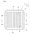
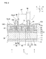
- IN laminate 12 and IP laminate 13 are formed on back surface 10b of semiconductor substrate 10. As shown in Fig. 1 , each of IN laminate 12 and IP laminate 13 is formed in a comb-teeth shape. IN laminate 12 and IP laminate 13 are configured to mesh with each other. Thus, on back surface 10b, IN laminate 12 and IP laminate 13 are alternately arranged along direction x perpendicular to intersection width direction y. IN laminate 12 and IP laminate 13 which are adjacent to each other in direction x are in contact with each other. More specifically, in this embodiment, substantially the entire back surface 10b is covered with IN laminate 12 and IP laminate 13. Note that width W1 (see Fig. 2 ) of IN laminate 12 and interval W2 of IN laminate 12 in direction x can be set to, for example, about 100 ⁇ m to 1.5 mm, respectively. Width W1 and interval W2 may be equal to or different from each other.
- IN laminate 12 is a laminate including i-type amorphous semiconductor layer 12i formed on back surface 10b and n-type amorphous semiconductor layer 12n formed on i-type amorphous semiconductor layer 12i.
- i-type amorphous semiconductor layer 12i is made of amorphous silicon containing hydrogen.
- the thickness of i-type amorphous semiconductor layer 12i is not particularly limited as long as it does not substantially contribute to power generation.
- the thickness of i-type amorphous semiconductor layer 12i can be set to, for example, about several ⁇ to 250 ⁇ .
- n-type amorphous semiconductor layer 12n is doped with an n-type dopant and has the same n-type conductivity as that of semiconductor substrate 10.
- n-type amorphous semiconductor layer 12n is made of n-type amorphous silicon containing hydrogen.
- the thickness of n-type amorphous semiconductor layer 12n is not particularly limited. The thickness of n-type amorphous semiconductor layer 12n can be set to, for example, about 20 ⁇ to 500 ⁇ .
- Insulating layer 18 is formed on both end portions of IN laminate 12 in direction x except for a center portion thereof. The center portion of IN laminate 12 in direction x is exposed from insulating layer 18.
- Width W3 of insulating layer 18 in direction x is not particularly limited but can be set to, for example, about 1/3 of width W1.
- interval W4 between insulating layers 18 in direction x is also not particularly limited but can be set to, for example, about 1/3 of width W1.
- Insulating layer 18 can be formed of, for example, silicon oxide, silicon nitride, silicon oxynitride or the like. Among those, it is preferable that insulating layer 18 is formed of silicon nitride. It is also preferable that insulating layer 18 contains hydrogen.
- IP laminate 13 is formed on a portion of back surface 10b exposed from IN laminate 12 and on end portions of insulating layer 18. Thus, both end portions of IP laminate 13 overlap with IN laminate 12 in height direction z.
- IP laminate 13 is a laminate including i-type amorphous semiconductor layer 13i formed on back surface 10b and p-type amorphous semiconductor layer 13p formed on i-type amorphous semiconductor layer 13i.
- i-type amorphous semiconductor layer 13i is made of amorphous silicon containing hydrogen.
- the thickness of i-type amorphous semiconductor layer 13i is not particularly limited as long as it does not substantially contribute to power generation.
- the thickness of i-type amorphous semiconductor layer 13i can be set to, for example, about several ⁇ to 250 ⁇ .
- p-type amorphous semiconductor layer 13p is an amorphous semiconductor layer which is doped with a p-type dopant and has a p-type conductivity.
- p-type amorphous semiconductor layer 13p is made of p-type amorphous silicon containing hydrogen.
- the thickness of p-type amorphous semiconductor layer 13p is not particularly limited. The thickness of p-type amorphous semiconductor layer 13p can be set to, for example, about 20 ⁇ to 500 ⁇ .
- a structure is formed in which i-type amorphous semiconductor layer 13i having the thickness that does not substantially contribute to power generation is provided between crystalline semiconductor substrate 10 and p-type amorphous semiconductor layer 13p.
- amorphous semiconductor layers 17, 12 and 13 contain hydrogen to improve passivation properties.
- n-side electrode 14 is formed as a first electrode to collect electrons.
- p-side electrode 15 is formed as a second electrode to collect holes.
- P-side electrode 15 and n-side electrode 14 are electrically insulated from each other. Note that interval W5 between n-side electrode 14 and p-side electrode 15 on insulating layer 18 can be set to, for example, about 1/3 of width W3.
- each of IN laminate 12 and IP laminate 13 is formed in the comb-teeth shape.
- n-side electrode 14 and p-side electrode 15 have bus bars 14A and 15A and multiple fingers 14B and 15B, respectively.
- each of n-side electrode 14 and p-side electrode 15 may be a so-called bus bar-less electrode including only multiple fingers and having no bus bar.
- bus bar 14A of n-side electrode 14 and bus bar 15A of p-side electrode 15 have substantially the same area.
- Fingers 14B of n-side electrode 14 are narrower than fingers 15B of p-side electrode 15. More specifically, width W6 of fingers 14B is smaller than width W7 of fingers 15B. Moreover, the number of fingers 14B is 1 fewer than the number of fingers 15B. Therefore, n-side electrode 14 is smaller in area than p-side electrode 15.
- W6/W7 is within the range of, for example, 0.5 to 1.
- N-side electrode 14 and p-side electrode 15 are not particularly limited as long as they can collect carriers.
- each of n-side electrode 14 and p-side electrode 15 includes a laminate of first to fourth conductive layers 19a to 19d.
- First conductive layer 19a can be formed of TCO (Transparent Conductive Oxide) or the like, such as ITO (indium tin oxide), for example.
- first conductive layer 19a is formed of ITO.
- the thickness of first conductive layer 19a can be set to, for example, about 50 to 100 nm.
- first conductive layer 19a can be formed by use of a thin-film formation method such as a sputtering method and a CVD (Chemical Vapor Deposition) method, for example.
- Second to fourth conductive layers 19b to 19d can be formed of metal or alloy such as Cu, for example.
- second and third conductive layers 19b and 19c are formed of Cu, respectively.
- Fourth conductive layer 19d is formed of Sn.
- the thicknesses of second to fourth conductive layers 19b to 19d are, for example, about 50 nm to 1 ⁇ m, about 10 ⁇ m to 20 ⁇ m, and about 1 ⁇ m to 5 ⁇ m, respectively.
- second conductive layer 19b among first to fourth conductive layers 19a to 19d forms a seed layer.
- the "seed layer” means a layer to be a source of plating growth.
- the seed layer is generally made of metal or alloy.
- Second conductive layer 19b as the seed layer can be formed by use of a thin-film formation method or the like, such as the sputtering method, a deposition method, a printing method or an ink jet method, besides a plating method.
- third and fourth conductive layers 19c and 19d are formed of plated films.
- semiconductor substrate 10 (see Figs. 4 and 2 ) is prepared.
- Step S1 light-receiving surface 10a and back surface 10b of semiconductor substrate 10 are cleaned.
- Semiconductor substrate 10 can be cleaned using, for example, an HF solution or the like. Note that, in this Step S1, a texture structure is formed on light-receiving surface 10a of semiconductor substrate 10. However, no texture structure is formed on back surface 10b.
- Step S2 i-type amorphous semiconductor layer 17i and n-type amorphous semiconductor layer 17n are formed on light-receiving surface 10a of semiconductor substrate 10.
- i-type amorphous semiconductor layer 21 and n-type amorphous semiconductor layer 22 are formed on back surface 10b.
- a method for forming i-type amorphous semiconductor layers 17i and 21 as well as n-type amorphous semiconductor layers 17n and 22 is not particularly limited.
- i-type amorphous semiconductor layers 17i and 21 as well as n-type amorphous semiconductor layers 17n and 22 can be formed using, for example, a CVD (Chemical Vapor Deposition) method, such as a plasma CVD method, or the like.
- CVD Chemical Vapor Deposition
- insulating layer 16 is formed on n-type amorphous semiconductor layer 17n, and insulating layer 23 is formed on n-type amorphous semiconductor layer 22.
- a method for forming insulating layers 16 and 23 is not particularly limited. Insulating layers 16 and 23 can be formed using a thin-film formation method or the like, such as a sputtering method and the CVD method, for example.
- Step S4 insulating layer 23 is etched to be partially removed. To be more specific, a portion of insulating layer 23, which is located on a region where a p-type semiconductor layer is to be joined to semiconductor substrate 10 in a subsequent step. Note that the etching of insulating layer 23 can be performed using an acid etchant such as the HF solution, for example, when insulating layer 23 is made of silicon oxide, silicon nitride or silicon oxynitride.
- an acid etchant such as the HF solution
- Step S5 using insulating layer 23 patterned in Step S4 as a mask, i-type amorphous semiconductor layer 21 and n-type amorphous semiconductor layer 22 are etched with an alkaline etchant. Thus, portions of i-type amorphous semiconductor layer 21 and n-type amorphous semiconductor layer 22, other than those covered with insulating layer 23 are removed. Accordingly, a portion of back surface 10b, above which no insulating layer 23 is located, is exposed. At the same time, i-type amorphous semiconductor layer 12i and n-type amorphous semiconductor layer 12n (see Fig. 2 ) are formed using semiconductor layers 21 and 22.
- insulating layer 23 is made of silicon oxide, silicon nitride or silicon oxynitride.
- an etching rate of insulating layer 23 using an acid etchant is high, an etching rate of insulating layer 23 using an alkaline etchant is low.
- semiconductor layers 21 and 22 are made of amorphous silicon.
- an etching rate using the acid etchant is low, and an etching rate using the alkaline etchant is high. Accordingly, with the acid etchant used in Step S4, insulating layer 23 is etched but semiconductor layers 21 and 22 are not substantially etched.
- Step S5 With the alkaline etchant used in Step S5, semiconductor layers 21 and 22 are etched but insulating layer 23 is not substantially etched. Therefore, in Steps S4 and S5, insulating layer 23 or semiconductor layers 21 and 22 can be selectively etched.
- semiconductor substrate 10 is prepared, which has back surface 10b as a first main surface and light-receiving surface 10a as a second main surface. Moreover, in semiconductor substrate 10, n-type amorphous semiconductor layer 12n made of an n-type semiconductor is formed on a part of back surface 10b, and insulating layer 23 is formed so as to cover n-type amorphous semiconductor layer 12n.
- Step S6 i-type amorphous semiconductor layer 24 and p-type amorphous semiconductor layer 25 are sequentially formed in this order so as to cover back surface 10b.
- a method for forming amorphous semiconductor layers 24 and 25 is not particularly limited. Amorphous semiconductor layers 24 and 25 can be formed using, for example, the CVD method or the like.
- Step S7 portions of amorphous semiconductor layers 24 and 25, which are located on insulating layer 23, are partially etched.
- i-type amorphous semiconductor layer 13i and p-type amorphous semiconductor layer 13p are formed from amorphous semiconductor layers 24 and 25.
- This Step S7 uses a first etching agent which etches amorphous semiconductor layers 24 and 25 at a higher etching rate than that for insulating layer 23. For this reason, among insulating layer 23 and amorphous semiconductor layers 24 and 25, amorphous semiconductor layers 24 and 25 are selectively etched.
- etching agent includes an etching paste and a viscosity-adjusted etching ink.
- insulating layer 23 is etched in Step S8.
- an exposed portion of insulating layer 23 is removed by etching, using a second etching agent, from above amorphous semiconductor layers 13i and 13p made of amorphous semiconductor layers 24 and 25 partially removed by the etching in Step S7.
- n-type amorphous semiconductor layer 12n is exposed, and insulating layer 18 is formed from insulating layer 23.
- This Step S8 uses the second etching agent which etches insulating layer 23 at a higher etching rate than that for amorphous semiconductor layers 24 and 25. For this reason, among insulating layer 23 and amorphous semiconductor layers 24 and 25, insulating layer 23 is selectively etched.
- solar cell substrate 20 is formed, which has a p-type surface (a surface of p-type amorphous semiconductor layer 13p) in one region of one main surface, and an n-type surface (a surface of n-type amorphous semiconductor layer 12n) in another region.
- Step S9 solar cell 1 can be completed by performing an electrode formation process to form n-side electrode 14 and p-side electrode 15 on n-type amorphous semiconductor layer 12n and p-type amorphous semiconductor layer 13p, respectively.
- Step S9-1 conductive layer 26 made of TCO and conductive layer 27 made of metal or alloy such as Cu are formed in this order using a CVD (Chemical Vapor Deposition) method such as a plasma CVD method or a thin-film formation method such as a sputtering method.
- CVD Chemical Vapor Deposition
- a plasma CVD method or a thin-film formation method such as a sputtering method.
- first and second conductive layers 19a and 19b are formed from conductive layers 26 and 27.
- second conductive layer 19b forms a seed layer as described above, seed layers are formed for n-side electrode 14 and p-side electrode 15, respectively.
- second conductive layer 19b as the seed layer includes first seed layer 19b1 positioned above n-type amorphous semiconductor layer 12n and second seed layer 19b2 positioned above p-type amorphous semiconductor layer 13p.
- first seed layer 19b1 and second seed layer 19b2 have different areas.
- the area of first seed layer 19b1 is smaller than that of second seed layer 19b2.
- a width of a portion forming fingers 14B of first seed layer 19b1 is smaller than that of a portion forming fingers 15B of second seed layer 19b2.
- conductive layers 26 and 27 can be performed using, for example, a photolithography method or the like.
- third conductive layer 19c made of Cu and fourth conductive layer 19d made of Sn are sequentially formed by electrolytic plating on first and second conductive layers 19a and 19b.
- n-side electrode 14 and p-side electrode 15 shown in Fig. 2 can be completed.
- first seed layer 19b1 is smaller than that of second seed layer 19b2.
- plated films having the same mass are formed on first and second seed layers 19b1 and 19b2, respectively.
- first plated film 19cd1 positioned on first seed layer 19b1 is larger in thickness than second plated film 19cd2 positioned on second seed layer 19b2, in conductive layers 19c and 19d.
- the same power source is used to supply currents to first seed layer 19b1 and second seed layer 19b2.
- the currents having the same magnitude are easily allowed to flow through both seed layers 19b1 and 19b2. Therefore, production of solar cell 1 is facilitated.
- both of the n-side electrode and the p-side electrode in large thickness.
- the n-side electrode and the p-side electrode, which are adjacent to each other are likely to come into contact with each other.
- the interval between the n-side electrode and the p-side electrode needs to be increased. This may lead to a situation where the areas of the n-side and p-side electrodes are reduced and the electrical resistance of the electrodes cannot be reduced.
- n-side electrode 14 which has a relatively small area and tends to have high electrical resistance, is formed to be taller than p-side electrode 15.
- n-side electrode 14 and p-side electrode 15 are unlikely to come into contact with each other. Accordingly, interval W5 between n-side electrode 14 and p-side electrode 15 can be reduced. As a result, the electrical resistance of n-side electrode 14 can be reduced more effectively.
- n-side electrode and the p-side electrode are formed in large thickness, a large stress is likely to act on the semiconductor substrate. As a result, warping of the semiconductor substrate is likely to occur.
- p-side electrode 15 is thinner than n-side electrode 14. Thus, a large stress is unlikely to act on semiconductor substrate 10. Therefore, the warping of semiconductor substrate 10 can be suppressed.
- a ratio of the thickness of n-side electrode 14 to the thickness of p-side electrode 15 is not particularly limited but is preferably within the range of 1 to 2.
- first and second plated films 19cd1 and 19cd2 can be adjusted by adjusting the currents to flow through first and second seed layers 19b1 and 19b2 during the formation of first and second plated films 19cd1 and 19cd2 in Step S9-1.
- allowing currents having different magnitudes to flow through first and second seed layers 19b1 and 19b2 enables formation of first and second plated films 19cd1 and 19cd2 having a thickness ratio different from that when the currents having the same magnitude are allowed to flow through first and second seed layers 19b1 and 19b2.
- first and second plated films 19cd1 and 19cd2 having the same thickness can also be formed. Therefore, the electrical resistance of n-side electrode 14 and p-side electrode 15 can be adjusted according to the requisite characteristics of solar cell 1.
- the invention is not limited to this configuration.
- heavily-doped n+ type region 31n may be formed in a portion of back surface 30b of n-type crystalline semiconductor substrate 30 by thermally diffusing an n-type dopant in a part of the portion of back surface 30b of crystalline semiconductor substrate 30.
- a heavily-doped n-type region may be formed by thermally diffusing an n-type dopant in one region of the back surface of n-type crystalline semiconductor substrate 30, and a p-type region may be formed by thermally diffusing a p-type dopant in another region.
- a surface of the n-type region which is more heavily doped than the semiconductor substrate forms an n-type surface of the invention, and a surface of the p-type region forms a p-type surface.
- first conductive layer 19a made of TCO does not particularly have to be provided.
- First conductive layer 19a made of TCO may be provided on the surface formed of the amorphous semiconductor layer, either the p-type surface or the n-type surface.
Landscapes
- Photovoltaic Devices (AREA)
- Engineering & Computer Science (AREA)
- Manufacturing & Machinery (AREA)
- Life Sciences & Earth Sciences (AREA)
- Sustainable Energy (AREA)
- Sustainable Development (AREA)
Abstract
Description
- The invention relates to a method of manufacturing a back junction solar cell, and a solar cell.
- In recent years, solar cells have been drawing keen attention as an energy source with a low impact on the environment. Thus, there have been active research and development in solar cells. Above all, the key issue is how to improve power generation efficiency of the solar cell. Thus, the research and development have been particularly active in a solar cell having improved power generation efficiency and in a method of manufacturing the same.
- As a solar cell having high power generation efficiency, the following
Patent Document 1 and the like, for example, proposes so-called a back junction solar cell having a p-type region and an n-type region formed on a back side of the solar cell. In this back junction solar cell, no electrode needs to be provided on a light-receiving side. Thus, the back junction solar cell can improve light reception efficiency. Therefore, more improved power generation efficiency can be achieved. Moreover, connection of solar cells by wiring can be performed only on the back side. Thus, wide wiring materials can be used. Therefore, a voltage drop due to connection of multiple solar cells by wiring can be prevented. - Patent Document 1: Japanese Patent Application Publication No.
2009-200267 - However, it is hard to say that ample studies have been done until now on an electrode structure or a method for forming electrodes to improve the power generation efficiency of the solar cell. Therefore, a significant challenge is to further improve the power generation efficiency of the solar cell by obtaining a more favorable electrode structure and method for forming electrodes.
- The invention is made in consideration of the foregoing problem. It is an objective of the invention to provide a method of manufacturing a solar cell having improved power generation efficiency and a solar cell having improved power generation efficiency.
- In a method of manufacturing a solar cell according to the invention, a solar cell substrate is formed which has one main surface and the other main surface and has a p-type surface and an n-type surface that are exposed on one region and another region in the one main surface, respectively. Seed layers in an electrically separated state are formed on the p-type surface and the n-type surface, respectively. A plated film is formed on the seed layer on each of the p-type surface and the n-type surface by an electrolytic plating method.
- A solar cell according to the invention includes a solar cell substrate and an electrode layer. The solar cell substrate has one main surface and the other main surface and has a p-type surface and an n-type surface which are exposed on one region and another region in the one main surface, respectively. The electrode layer is formed on each of the p-type surface and the n-type surface. An electrode formed on one of the p-type surface and the n-type surface, which has a larger area, is larger in thickness than an electrode formed on the other surface.
- The invention can provide a method of manufacturing a solar cell having improved power generation efficiency and a solar cell having improved power generation efficiency.
-
-
Fig. 1 is a schematic plan view of a solar cell according to a first embodiment. -
Fig. 2 is a schematic partial cross-sectional view taken along the line II-II inFig. 1 . -
Fig. 3 is a flowchart showing steps of production of the solar cell according to the first embodiment. -
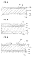
Fig. 4 is a schematic cross-sectional view for explaining the steps of production of the solar cell. -
Fig. 5 is a schematic cross-sectional view for explaining the steps of production of the solar cell. -
Fig. 6 is a schematic cross-sectional view for explaining the steps of production of the solar cell. -
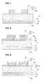
Fig. 7 is a schematic cross-sectional view for explaining the steps of production of the solar cell. -
Fig. 8 is a schematic cross-sectional view for explaining the steps of production of the solar cell. -
Fig. 9 is a schematic cross-sectional view for explaining the steps of production of the solar cell. -
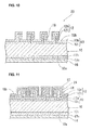
Fig. 10 is a schematic cross-sectional view for explaining the steps of production of the solar cell. -
Fig. 11 is a schematic cross-sectional view for explaining the steps of production of the solar cell. -
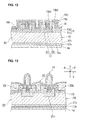
Fig. 12 is a schematic cross-sectional view for explaining the steps of production of the solar cell. -
Fig. 13 is a schematic cross-sectional view of a solar cell according to a second embodiment. - Examples of preferred embodiments of the invention are described below. However, the following embodiments are provided as examples but are not intended to limit the invention thereto.
- Note that, in the drawings to be referred to in the embodiments and the like, members having substantially the same functions are denoted by the same reference numerals. In addition, the drawings to be referred to in the embodiments and the like are schematic and ratios of dimensions and the like are different from actual ones. Moreover, the drawings also include portions having different dimensional relationships and ratios from each other. Therefore, specific dimensions and the like should be determined in consideration of the following description.
- First, a configuration of
solar cell 1 to be produced in this embodiment is described in detail with reference toFigs. 1 and2 . -
Solar cell 1 is a back junction solar cell. Note that whensolar cell 1 of this embodiment cannot achieve a sufficiently large output by itself, multiplesolar cells 1 may be connected by wiring and used as a solar cell module. -
Solar cell 1 includessemiconductor substrate 10.Semiconductor substrate 10 has light-receiving surface 10a as a second main surface andback surface 10b as a first main surface.Semiconductor substrate 10 receiveslight 11 on light-receivingsurface 10a to generate carriers. Here, the carriers are holes and electrons to be generated bysemiconductor substrate 10 absorbing light. -
Semiconductor substrate 10 is formed using a crystalline semiconductor substrate having an n-type or p-type conductivity. Specific examples of the crystalline semiconductor substrate include crystalline silicon substrates such as a single-crystal silicon substrate and a polycrystalline silicon substrate, for example. - Note that the semiconductor substrate can also be formed using semiconductor substrates other than the crystalline semiconductor substrate. For example, a compound semiconductor substrate made of GaAs, InP or the like can be used in place of
semiconductor substrate 10. In this embodiment, description is given below of an example wheresemiconductor substrate 10 is formed using an n-type crystalline silicon substrate. - On light-receiving
surface 10a ofsemiconductor substrate 10, i-typeamorphous semiconductor layer 17i is formed, which is made of an intrinsic amorphous semiconductor (the intrinsic semiconductor is hereinafter referred to as the "i-type semiconductor"). To be more specific, in this embodiment, i-typeamorphous semiconductor layer 17i is formed of i-type amorphous silicon containing hydrogen. The thickness of i-typeamorphous semiconductor layer 17i is not particularly limited as long as it does not substantially contribute to power generation. The thickness of i-typeamorphous semiconductor layer 17i can be set to, for example, about several Å to 250 Å. - Note that, in the invention, the "amorphous semiconductor" includes a microcrystalline semiconductor. The microcrystalline semiconductor is a semiconductor in which an average particle size of semiconductor crystal deposited in the amorphous semiconductor is in the range of about 1 to 80 nm.
- On i-type
amorphous semiconductor layer 17i, n-typeamorphous semiconductor layer 17n is formed, which has the same conductivity as that ofsemiconductor substrate 10. N-typeamorphous semiconductor layer 17n is an amorphous semiconductor layer which is doped with an n-type dopant and has the n-type conductivity. To be more specific, in this embodiment, n-typeamorphous semiconductor layer 17n is made of n-type amorphous silicon containing hydrogen. The thickness of n-typeamorphous semiconductor layer 17n is not particularly limited. The thickness of n-typeamorphous semiconductor layer 17n can be set to, for example, about 20 Å to 500 Å. - On n-type
amorphous semiconductor layer 17n, insulatinglayer 16 is formed, which serves both as an antireflection film and as a protective film. Insulatinglayer 16 can be formed of, for example, silicon oxide, silicon nitride or silicon oxynitride. The thickness of insulatinglayer 16 can be set according to antireflection properties and the like of the antireflection film to be provided. The thickness of insulatinglayer 16 can be set to, for example, about 80 nm to 1 µm. - The laminate structure of i-type
amorphous semiconductor layer 17i, n-typeamorphous semiconductor layer 17n and insulatinglayer 16 described above functions as a passivation layer and as an antireflection film forsemiconductor substrate 10. - On
back surface 10b ofsemiconductor substrate 10, INlaminate 12 andIP laminate 13 are formed. As shown inFig. 1 , each ofIN laminate 12 andIP laminate 13 is formed in a comb-teeth shape. INlaminate 12 andIP laminate 13 are configured to mesh with each other. Thus, onback surface 10b, INlaminate 12 andIP laminate 13 are alternately arranged along direction x perpendicular to intersection width direction y. INlaminate 12 andIP laminate 13 which are adjacent to each other in direction x are in contact with each other. More specifically, in this embodiment, substantially theentire back surface 10b is covered withIN laminate 12 andIP laminate 13. Note that width W1 (seeFig. 2 ) ofIN laminate 12 and interval W2 ofIN laminate 12 in direction x can be set to, for example, about 100 µm to 1.5 mm, respectively. Width W1 and interval W2 may be equal to or different from each other. - IN
laminate 12 is a laminate including i-typeamorphous semiconductor layer 12i formed onback surface 10b and n-typeamorphous semiconductor layer 12n formed on i-typeamorphous semiconductor layer 12i. As in the case of i-typeamorphous semiconductor layer 17i described above, i-typeamorphous semiconductor layer 12i is made of amorphous silicon containing hydrogen. The thickness of i-typeamorphous semiconductor layer 12i is not particularly limited as long as it does not substantially contribute to power generation. The thickness of i-typeamorphous semiconductor layer 12i can be set to, for example, about several Å to 250 Å. - As in the case of n-type
amorphous semiconductor layer 17n, n-typeamorphous semiconductor layer 12n is doped with an n-type dopant and has the same n-type conductivity as that ofsemiconductor substrate 10. To be more specific, in this embodiment, n-typeamorphous semiconductor layer 12n is made of n-type amorphous silicon containing hydrogen. The thickness of n-typeamorphous semiconductor layer 12n is not particularly limited. The thickness of n-typeamorphous semiconductor layer 12n can be set to, for example, about 20 Å to 500 Å. - Insulating
layer 18 is formed on both end portions ofIN laminate 12 in direction x except for a center portion thereof. The center portion ofIN laminate 12 in direction x is exposed from insulatinglayer 18. Width W3 of insulatinglayer 18 in direction x is not particularly limited but can be set to, for example, about 1/3 of width W1. Moreover, interval W4 between insulatinglayers 18 in direction x is also not particularly limited but can be set to, for example, about 1/3 of width W1. - The material of insulating
layer 18 is not particularly limited. Insulatinglayer 18 can be formed of, for example, silicon oxide, silicon nitride, silicon oxynitride or the like. Among those, it is preferable that insulatinglayer 18 is formed of silicon nitride. It is also preferable that insulatinglayer 18 contains hydrogen. -
IP laminate 13 is formed on a portion ofback surface 10b exposed fromIN laminate 12 and on end portions of insulatinglayer 18. Thus, both end portions ofIP laminate 13 overlap withIN laminate 12 in height direction z. -
IP laminate 13 is a laminate including i-type amorphous semiconductor layer 13i formed onback surface 10b and p-typeamorphous semiconductor layer 13p formed on i-type amorphous semiconductor layer 13i. - i-type amorphous semiconductor layer 13i is made of amorphous silicon containing hydrogen. The thickness of i-type amorphous semiconductor layer 13i is not particularly limited as long as it does not substantially contribute to power generation. The thickness of i-type amorphous semiconductor layer 13i can be set to, for example, about several Å to 250 Å.
- p-type
amorphous semiconductor layer 13p is an amorphous semiconductor layer which is doped with a p-type dopant and has a p-type conductivity. To be more specific, in this embodiment, p-typeamorphous semiconductor layer 13p is made of p-type amorphous silicon containing hydrogen. The thickness of p-typeamorphous semiconductor layer 13p is not particularly limited. The thickness of p-typeamorphous semiconductor layer 13p can be set to, for example, about 20 Å to 500 Å. - As described above, in this embodiment, a structure is formed in which i-type amorphous semiconductor layer 13i having the thickness that does not substantially contribute to power generation is provided between
crystalline semiconductor substrate 10 and p-typeamorphous semiconductor layer 13p. By adopting such a structure in this embodiment, minority carriers can be prevented from being recombined at the junction interface betweensemiconductor substrate 10 andIP laminate 13. As a result, photoelectric conversion efficiency can be improved. - Note that it is preferable that amorphous semiconductor layers 17, 12 and 13 contain hydrogen to improve passivation properties.
- On n-type
amorphous semiconductor layer 12n, n-side electrode 14 is formed as a first electrode to collect electrons. On the other hand, on p-typeamorphous semiconductor layer 13p, p-side electrode 15 is formed as a second electrode to collect holes. P-side electrode 15 and n-side electrode 14 are electrically insulated from each other. Note that interval W5 between n-side electrode 14 and p-side electrode 15 on insulatinglayer 18 can be set to, for example, about 1/3 of width W3. - As described above, in this embodiment, each of
IN laminate 12 andIP laminate 13 is formed in the comb-teeth shape. Thus, as shown inFig. 1 , n-side electrode 14 and p-side electrode 15 havebus bars multiple fingers side electrode 14 and p-side electrode 15 may be a so-called bus bar-less electrode including only multiple fingers and having no bus bar. - In this embodiment,
bus bar 14A of n-side electrode 14 andbus bar 15A of p-side electrode 15 have substantially the same area.Fingers 14B of n-side electrode 14 are narrower thanfingers 15B of p-side electrode 15. More specifically, width W6 offingers 14B is smaller than width W7 offingers 15B. Moreover, the number offingers 14B is 1 fewer than the number offingers 15B. Therefore, n-side electrode 14 is smaller in area than p-side electrode 15. - Note that it is preferable that W6/W7 is within the range of, for example, 0.5 to 1.
- N-
side electrode 14 and p-side electrode 15 are not particularly limited as long as they can collect carriers. In this embodiment, each of n-side electrode 14 and p-side electrode 15 includes a laminate of first to fourthconductive layers 19a to 19d. - First
conductive layer 19a can be formed of TCO (Transparent Conductive Oxide) or the like, such as ITO (indium tin oxide), for example. To be more specific, in this embodiment, firstconductive layer 19a is formed of ITO. The thickness of firstconductive layer 19a can be set to, for example, about 50 to 100 nm. Note that firstconductive layer 19a can be formed by use of a thin-film formation method such as a sputtering method and a CVD (Chemical Vapor Deposition) method, for example. - Second to fourth
conductive layers 19b to 19d can be formed of metal or alloy such as Cu, for example. To be more specific, in this embodiment, second and thirdconductive layers conductive layer 19d is formed of Sn. The thicknesses of second to fourthconductive layers 19b to 19d are, for example, about 50 nm to 1 µm, about 10 µm to 20 µm, and about 1 µm to 5 µm, respectively. - In this embodiment, second
conductive layer 19b among first to fourthconductive layers 19a to 19d forms a seed layer. Here, the "seed layer" means a layer to be a source of plating growth. The seed layer is generally made of metal or alloy. Secondconductive layer 19b as the seed layer can be formed by use of a thin-film formation method or the like, such as the sputtering method, a deposition method, a printing method or an ink jet method, besides a plating method. - In this embodiment, third and fourth
conductive layers - Next, a method of manufacturing
solar cell 1 of this embodiment is described mainly with reference toFigs. 3 to 13 . - First, semiconductor substrate 10 (see
Figs. 4 and2 ) is prepared. Next, in Step S1, light-receivingsurface 10a and backsurface 10b ofsemiconductor substrate 10 are cleaned.Semiconductor substrate 10 can be cleaned using, for example, an HF solution or the like. Note that, in this Step S1, a texture structure is formed on light-receivingsurface 10a ofsemiconductor substrate 10. However, no texture structure is formed onback surface 10b. - Next, in Step S2, i-type
amorphous semiconductor layer 17i and n-typeamorphous semiconductor layer 17n are formed on light-receivingsurface 10a ofsemiconductor substrate 10. At the same time, i-typeamorphous semiconductor layer 21 and n-typeamorphous semiconductor layer 22 are formed onback surface 10b. A method for forming i-typeamorphous semiconductor layers amorphous semiconductor layers amorphous semiconductor layers amorphous semiconductor layers - Then, in Step S3, insulating
layer 16 is formed on n-typeamorphous semiconductor layer 17n, and insulatinglayer 23 is formed on n-typeamorphous semiconductor layer 22. Note that a method for forming insulatinglayers layers - Next, in Step S4, insulating
layer 23 is etched to be partially removed. To be more specific, a portion of insulatinglayer 23, which is located on a region where a p-type semiconductor layer is to be joined tosemiconductor substrate 10 in a subsequent step. Note that the etching of insulatinglayer 23 can be performed using an acid etchant such as the HF solution, for example, when insulatinglayer 23 is made of silicon oxide, silicon nitride or silicon oxynitride. - Next, in Step S5, using insulating
layer 23 patterned in Step S4 as a mask, i-typeamorphous semiconductor layer 21 and n-typeamorphous semiconductor layer 22 are etched with an alkaline etchant. Thus, portions of i-typeamorphous semiconductor layer 21 and n-typeamorphous semiconductor layer 22, other than those covered with insulatinglayer 23 are removed. Accordingly, a portion ofback surface 10b, above which no insulatinglayer 23 is located, is exposed. At the same time, i-typeamorphous semiconductor layer 12i and n-typeamorphous semiconductor layer 12n (seeFig. 2 ) are formed usingsemiconductor layers - Here, as described above, in this embodiment, insulating
layer 23 is made of silicon oxide, silicon nitride or silicon oxynitride. Thus, while an etching rate of insulatinglayer 23 using an acid etchant is high, an etching rate of insulatinglayer 23 using an alkaline etchant is low. On the other hand, semiconductor layers 21 and 22 are made of amorphous silicon. Thus, as tosemiconductor layers layer 23 is etched but semiconductor layers 21 and 22 are not substantially etched. On the other hand, with the alkaline etchant used in Step S5, semiconductor layers 21 and 22 are etched but insulatinglayer 23 is not substantially etched. Therefore, in Steps S4 and S5, insulatinglayer 23 orsemiconductor layers - As described above, in Steps S1 to S5,
semiconductor substrate 10 is prepared, which has backsurface 10b as a first main surface and light-receivingsurface 10a as a second main surface. Moreover, insemiconductor substrate 10, n-typeamorphous semiconductor layer 12n made of an n-type semiconductor is formed on a part ofback surface 10b, and insulatinglayer 23 is formed so as to cover n-typeamorphous semiconductor layer 12n. - Next, in Step S6, i-type
amorphous semiconductor layer 24 and p-typeamorphous semiconductor layer 25 are sequentially formed in this order so as to cover backsurface 10b. A method for forming amorphous semiconductor layers 24 and 25 is not particularly limited. Amorphous semiconductor layers 24 and 25 can be formed using, for example, the CVD method or the like. - Thereafter, in Step S7, portions of amorphous semiconductor layers 24 and 25, which are located on insulating
layer 23, are partially etched. Thus, i-type amorphous semiconductor layer 13i and p-typeamorphous semiconductor layer 13p are formed from amorphous semiconductor layers 24 and 25. - This Step S7 uses a first etching agent which etches amorphous semiconductor layers 24 and 25 at a higher etching rate than that for insulating
layer 23. For this reason, among insulatinglayer 23 and amorphous semiconductor layers 24 and 25, amorphous semiconductor layers 24 and 25 are selectively etched. - Note that the "etching agent" includes an etching paste and a viscosity-adjusted etching ink.
- Next, insulating
layer 23 is etched in Step S8. To be more specific, an exposed portion of insulatinglayer 23 is removed by etching, using a second etching agent, from aboveamorphous semiconductor layers 13i and 13p made of amorphous semiconductor layers 24 and 25 partially removed by the etching in Step S7. Thus, n-typeamorphous semiconductor layer 12n is exposed, and insulatinglayer 18 is formed from insulatinglayer 23. - This Step S8 uses the second etching agent which etches insulating
layer 23 at a higher etching rate than that for amorphous semiconductor layers 24 and 25. For this reason, among insulatinglayer 23 and amorphous semiconductor layers 24 and 25, insulatinglayer 23 is selectively etched. - As described above, in Steps S1 to S8,
solar cell substrate 20 is formed, which has a p-type surface (a surface of p-typeamorphous semiconductor layer 13p) in one region of one main surface, and an n-type surface (a surface of n-typeamorphous semiconductor layer 12n) in another region. - Subsequently, in Step S9,
solar cell 1 can be completed by performing an electrode formation process to form n-side electrode 14 and p-side electrode 15 on n-typeamorphous semiconductor layer 12n and p-typeamorphous semiconductor layer 13p, respectively. - To be more specific, first, in Step S9-1,
conductive layer 26 made of TCO andconductive layer 27 made of metal or alloy such as Cu are formed in this order using a CVD (Chemical Vapor Deposition) method such as a plasma CVD method or a thin-film formation method such as a sputtering method. Thereafter, as shown inFig. 12 , portions ofconductive layers layer 18, are divided. Thus, first and secondconductive layers conductive layers conductive layer 19b forms a seed layer as described above, seed layers are formed for n-side electrode 14 and p-side electrode 15, respectively. - As shown in
Fig. 12 , secondconductive layer 19b as the seed layer includes first seed layer 19b1 positioned above n-typeamorphous semiconductor layer 12n and second seed layer 19b2 positioned above p-typeamorphous semiconductor layer 13p. In this embodiment, first seed layer 19b1 and second seed layer 19b2 have different areas. To be more specific, the area of first seed layer 19b1 is smaller than that of second seed layer 19b2. Moreover, a width of aportion forming fingers 14B of first seed layer 19b1 is smaller than that of aportion forming fingers 15B of second seed layer 19b2. - Note that the division of
conductive layers - Next, third
conductive layer 19c made of Cu and fourthconductive layer 19d made of Sn are sequentially formed by electrolytic plating on first and secondconductive layers side electrode 14 and p-side electrode 15 shown inFig. 2 can be completed. - Here, in this embodiment, as described above, the area of first seed layer 19b1 is smaller than that of second seed layer 19b2. Moreover, when currents having the same magnitude are allowed to flow through first seed layer 19b1 and second seed layer 19b2, plated films having the same mass are formed on first and second seed layers 19b1 and 19b2, respectively. Thus, when the currents having the same magnitude are allowed to flow through first seed layer 19b1 and second seed layer 19b2, first plated film 19cd1 positioned on first seed layer 19b1 is larger in thickness than second plated film 19cd2 positioned on second seed layer 19b2, in
conductive layers side electrode 14, which has a relatively small area and tends to have high electrical resistance, can be reduced effectively. As a result, power generation efficiency ofsolar cell 1 can be further improved. - Here, the same power source is used to supply currents to first seed layer 19b1 and second seed layer 19b2. Thus, the currents having the same magnitude are easily allowed to flow through both seed layers 19b1 and 19b2. Therefore, production of
solar cell 1 is facilitated. - For example, from the viewpoint of reduction of the electrical resistance of the electrodes, it is also conceivable to form both of the n-side electrode and the p-side electrode in large thickness. However, in such a case, the n-side electrode and the p-side electrode, which are adjacent to each other, are likely to come into contact with each other. For this reason, the interval between the n-side electrode and the p-side electrode needs to be increased. This may lead to a situation where the areas of the n-side and p-side electrodes are reduced and the electrical resistance of the electrodes cannot be reduced.
- On the other hand, in this embodiment, n-
side electrode 14, which has a relatively small area and tends to have high electrical resistance, is formed to be taller than p-side electrode 15. Thus, n-side electrode 14 and p-side electrode 15 are unlikely to come into contact with each other. Accordingly, interval W5 between n-side electrode 14 and p-side electrode 15 can be reduced. As a result, the electrical resistance of n-side electrode 14 can be reduced more effectively. - Moreover, when both of the n-side electrode and the p-side electrode are formed in large thickness, a large stress is likely to act on the semiconductor substrate. As a result, warping of the semiconductor substrate is likely to occur. In this embodiment, on the other hand, p-
side electrode 15 is thinner than n-side electrode 14. Thus, a large stress is unlikely to act onsemiconductor substrate 10. Therefore, the warping ofsemiconductor substrate 10 can be suppressed. - Note that a ratio of the thickness of n-
side electrode 14 to the thickness of p-side electrode 15 ((thickness of n-side electrode 14) / (thickness of p-side electrode 15)) is not particularly limited but is preferably within the range of 1 to 2. - Moreover, the thicknesses of first and second plated films 19cd1 and 19cd2 can be adjusted by adjusting the currents to flow through first and second seed layers 19b1 and 19b2 during the formation of first and second plated films 19cd1 and 19cd2 in Step S9-1. For example, allowing currents having different magnitudes to flow through first and second seed layers 19b1 and 19b2 enables formation of first and second plated films 19cd1 and 19cd2 having a thickness ratio different from that when the currents having the same magnitude are allowed to flow through first and second seed layers 19b1 and 19b2. To be more specific, first and second plated films 19cd1 and 19cd2 having the same thickness can also be formed. Therefore, the electrical resistance of n-
side electrode 14 and p-side electrode 15 can be adjusted according to the requisite characteristics ofsolar cell 1. - Furthermore, in the first embodiment, the description has been given of the example where the crystalline semiconductor substrate having the n-type conductivity is used as
semiconductor substrate 10, and n-typeamorphous semiconductor layer 12n and p-typeamorphous semiconductor layer 13p are formed onsemiconductor substrate 10 as shown inFig. 2 . However, the invention is not limited to this configuration. - For example, as shown in
Fig. 13 , heavily-dopedn+ type region 31n may be formed in a portion ofback surface 30b of n-typecrystalline semiconductor substrate 30 by thermally diffusing an n-type dopant in a part of the portion ofback surface 30b ofcrystalline semiconductor substrate 30. - Moreover, a heavily-doped n-type region may be formed by thermally diffusing an n-type dopant in one region of the back surface of n-type
crystalline semiconductor substrate 30, and a p-type region may be formed by thermally diffusing a p-type dopant in another region. In this case, a surface of the n-type region which is more heavily doped than the semiconductor substrate forms an n-type surface of the invention, and a surface of the p-type region forms a p-type surface. - Furthermore, when the p-type surface or the n-type surface is formed of the surface of the crystalline semiconductor substrate, first
conductive layer 19a made of TCO does not particularly have to be provided. Firstconductive layer 19a made of TCO may be provided on the surface formed of the amorphous semiconductor layer, either the p-type surface or the n-type surface. -
1 solar cell 10 semiconductor substrate 10a light-receiving surface 10b back surface 11 light 12 IN laminate 12i i-type amorphous semiconductor layer 12n n-type amorphous semiconductor layer 13 IP laminate 13i i-type amorphous semiconductor layer 13p p-type amorphous semiconductor layer 14 n-side electrode 15 p- side electrode 14A, 15A bus bar 14B, 15B finger 16 insulating layer 17i i-type amorphous semiconductor layer 17n n-type amorphous semiconductor layer 18 insulating layer 19a first conductive layer 19b second conductive layer 19b1 first seed layer 19b2 second seed layer 19c third conductive layer 19d fourth conductive layer 19cd1 first plated film 19cd2 second plated film 20 solar cell substrate 21 i-type amorphous semiconductor layer 22 n-type amorphous semiconductor layer 23 insulating layer 24 i-type amorphous semiconductor layer 25 p-type amorphous semiconductor layer 26, 27 conductive layer 30 amorphous semiconductor substrate 30b back surface 31n n+ type region
Claims (10)
- Amethod of manufacturing a solar cell, comprising:forming a solar cell substrate having one main surface and the other main surface and having a p-type surface and an n-type surface which are exposed on one region and another region in the one main surface, respectively;forming seed layers in an electrically separated state on the p-type surface and the n-type surface, respectively; andforming a plated film on the seed layer on each of the p-type surface and the n-type surface by an electrolytic plating method.
- The method of manufacturing a solar cell, according to claim 1, wherein
a common power source is used to supply currents to the seed layers on the p-type surface and the n-type surface. - The method of manufacturing a solar cell, according to one of claims 1 and 2, wherein
the step of forming the seed layers in the electrically separated state on the p-type surface and the n-type surface, respectively, includes a step of forming a continuous metal layer on the p-type surface and on the n-type surface and then electrically separating the metal layer. - The method of manufacturing a solar cell, according to any one of claims 1 to 3, wherein
the solar cell substrate has a first conductivity type of semiconductor substrate,
the method further comprising the step of:forming an insulating layer on one of the p-type surface and the n-type surface, which has the same conductivity type as that of the semiconductor substrate,whereinthe metal layer is formed to be continuous on the p-type surface and the n-type surface including the insulating layer, and then the electrically separated seed layers are formed by removing the metal layer on the insulating layer. - The method of manufacturing a solar cell, according to any one of claims 1 to 4, wherein
the plated film formed on one of the p-type surface and the n-type surface, which has a larger area than the other of the p-type surface and the n-type surface, is larger in thickness than the plated film formed on the other surface. - The method of manufacturing a solar cell, according to any one of claims 1 to 5, wherein
the other main surface of the solar cell substrate is a light-receiving surface. - The method of manufacturing a solar cell, according to claim 6, wherein
the solar cell substrate has a passivation film on the other main surface. - A solar cell comprising:a solar cell substrate having one main surface and the other main surface and having a p-type surface and an n-type surface which are exposed on one region and another region in the one main surface, respectively; andan electrode layer formed on each of the p-type surface and the n-type surface,wherein an electrode formed on one of the p-type surface and the n-type surface, which has a larger area which has a larger area than the other of the p-type surface and the n-type surface, is larger in thickness than an electrode formed on the other surface.
- The solar cell according to claim 8, wherein
the other main surface is a light-receiving surface. - The solar cell according to claim 8, wherein
the solar cell substrate has a passivation film on the other main surface.
Applications Claiming Priority (2)
| Application Number | Priority Date | Filing Date | Title |
|---|---|---|---|
| JP2010171340A JP5485062B2 (en) | 2010-07-30 | 2010-07-30 | Solar cell manufacturing method and solar cell |
| PCT/JP2011/067281 WO2012014983A1 (en) | 2010-07-30 | 2011-07-28 | Process for production of solar cell, and solar cell |
Publications (2)
| Publication Number | Publication Date |
|---|---|
| EP2600414A1 true EP2600414A1 (en) | 2013-06-05 |
| EP2600414A4 EP2600414A4 (en) | 2014-10-22 |
Family
ID=45530183
Family Applications (1)
| Application Number | Title | Priority Date | Filing Date |
|---|---|---|---|
| EP11812572.3A Withdrawn EP2600414A4 (en) | 2010-07-30 | 2011-07-28 | METHOD FOR MANUFACTURING SOLAR CELL AND SOLAR CELL |
Country Status (4)
| Country | Link |
|---|---|
| US (1) | US10134940B2 (en) |
| EP (1) | EP2600414A4 (en) |
| JP (1) | JP5485062B2 (en) |
| WO (1) | WO2012014983A1 (en) |
Cited By (1)
| Publication number | Priority date | Publication date | Assignee | Title |
|---|---|---|---|---|
| EP2851963A1 (en) * | 2013-09-24 | 2015-03-25 | Sanyo Electric Co., Ltd | Solar cell |
Families Citing this family (14)
| Publication number | Priority date | Publication date | Assignee | Title |
|---|---|---|---|---|
| JPWO2012132835A1 (en) * | 2011-03-25 | 2014-07-28 | 三洋電機株式会社 | Solar cell |
| WO2012132655A1 (en) * | 2011-03-25 | 2012-10-04 | 三洋電機株式会社 | Back-junction photoelectric conversion element and method for manufacturing back-junction photoelectric conversion element |
| EP2690667A4 (en) * | 2011-03-25 | 2014-10-08 | Sanyo Electric Co | METHOD FOR PRODUCING PHOTOELECTRIC CONVERSION DEVICE |
| WO2012132654A1 (en) * | 2011-03-25 | 2012-10-04 | 三洋電機株式会社 | Back-junction photoelectric conversion element and method for manufacturing back-junction photoelectric conversion element |
| JP6312060B2 (en) * | 2012-10-31 | 2018-04-18 | パナソニックIpマネジメント株式会社 | Solar cell |
| JP6206843B2 (en) * | 2013-09-09 | 2017-10-04 | パナソニックIpマネジメント株式会社 | Solar cell |
| JP6423373B2 (en) * | 2014-02-10 | 2018-11-14 | シャープ株式会社 | Photoelectric conversion element and solar cell module including the same |
| JP6350858B2 (en) | 2014-05-26 | 2018-07-04 | パナソニックIpマネジメント株式会社 | Solar cell manufacturing method and solar cell |
| JP6369680B2 (en) | 2014-05-30 | 2018-08-08 | パナソニックIpマネジメント株式会社 | Solar cell |
| WO2016143698A1 (en) * | 2015-03-11 | 2016-09-15 | シャープ株式会社 | Photoelectric conversion element |
| CN107112375B (en) | 2015-03-31 | 2020-05-12 | 株式会社钟化 | Solar cell and solar cell module |
| WO2018181499A1 (en) * | 2017-03-31 | 2018-10-04 | 株式会社カネカ | Photoelectric conversion element and photoelectric conversion element manufacturing method |
| CN114242810B (en) * | 2022-02-24 | 2022-04-29 | 广东爱旭科技有限公司 | Electrode structures, cells, assemblies, and battery systems for back-contact cells |
| CN118472056B (en) * | 2024-07-10 | 2025-04-29 | 隆基绿能科技股份有限公司 | Back contact battery, manufacturing method thereof and photovoltaic module |
Family Cites Families (17)
| Publication number | Priority date | Publication date | Assignee | Title |
|---|---|---|---|---|
| US7388147B2 (en) * | 2003-04-10 | 2008-06-17 | Sunpower Corporation | Metal contact structure for solar cell and method of manufacture |
| JP2005260157A (en) * | 2004-03-15 | 2005-09-22 | Sharp Corp | Solar cell and solar cell module |
| FR2880989B1 (en) * | 2005-01-20 | 2007-03-09 | Commissariat Energie Atomique | SEMICONDUCTOR DEVICE WITH HETEROJUNCTIONS AND INTERDIGITAL STRUCTURE |
| DE102006027737A1 (en) * | 2006-06-10 | 2007-12-20 | Hahn-Meitner-Institut Berlin Gmbh | Unilaterally contacted solar cell with plated-through holes and method of manufacture |
| US7799182B2 (en) * | 2006-12-01 | 2010-09-21 | Applied Materials, Inc. | Electroplating on roll-to-roll flexible solar cell substrates |
| WO2009052511A2 (en) * | 2007-10-18 | 2009-04-23 | Belano Holdings, Ltd. | Mono-silicon solar cells |
| DE102008030880A1 (en) * | 2007-12-11 | 2009-06-18 | Institut Für Solarenergieforschung Gmbh | Rear contact solar cell with large backside emitter areas and manufacturing method therefor |
| EP2239788A4 (en) * | 2008-01-30 | 2017-07-12 | Kyocera Corporation | Solar battery element and solar battery element manufacturing method |
| DE102008013446A1 (en) * | 2008-02-15 | 2009-08-27 | Ersol Solar Energy Ag | Process for producing monocrystalline n-silicon solar cells and solar cell, produced by such a process |
| JP5230222B2 (en) * | 2008-02-21 | 2013-07-10 | 三洋電機株式会社 | Solar cell |
| DE102008028104A1 (en) * | 2008-06-13 | 2009-12-24 | Deutsche Cell Gmbh | Metallization process for solar cells |
| JP2010123859A (en) * | 2008-11-21 | 2010-06-03 | Kyocera Corp | Solar battery element and production process of solar battery element |
| US8242354B2 (en) * | 2008-12-04 | 2012-08-14 | Sunpower Corporation | Backside contact solar cell with formed polysilicon doped regions |
| JP2010147324A (en) * | 2008-12-19 | 2010-07-01 | Kyocera Corp | Solar cell element and method of manufacturing solar cell element |
| US8409911B2 (en) * | 2009-02-24 | 2013-04-02 | Sunpower Corporation | Methods for metallization of solar cells |
| CN102725858B (en) * | 2010-01-26 | 2015-12-09 | 三洋电机株式会社 | Solar cell and manufacture method thereof |
| EP2395554A3 (en) * | 2010-06-14 | 2015-03-11 | Imec | Fabrication method for interdigitated back contact photovoltaic cells |
-
2010
- 2010-07-30 JP JP2010171340A patent/JP5485062B2/en not_active Expired - Fee Related
-
2011
- 2011-07-28 WO PCT/JP2011/067281 patent/WO2012014983A1/en not_active Ceased
- 2011-07-28 EP EP11812572.3A patent/EP2600414A4/en not_active Withdrawn
-
2013
- 2013-01-28 US US13/751,349 patent/US10134940B2/en not_active Expired - Fee Related
Cited By (2)
| Publication number | Priority date | Publication date | Assignee | Title |
|---|---|---|---|---|
| EP2851963A1 (en) * | 2013-09-24 | 2015-03-25 | Sanyo Electric Co., Ltd | Solar cell |
| US9780241B2 (en) | 2013-09-24 | 2017-10-03 | Panasonic Intellectual Property Management Co., Ltd. | Solar cell |
Also Published As
| Publication number | Publication date |
|---|---|
| JP5485062B2 (en) | 2014-05-07 |
| US10134940B2 (en) | 2018-11-20 |
| US20130180585A1 (en) | 2013-07-18 |
| JP2012033666A (en) | 2012-02-16 |
| WO2012014983A1 (en) | 2012-02-02 |
| EP2600414A4 (en) | 2014-10-22 |
Similar Documents
| Publication | Publication Date | Title |
|---|---|---|
| US10134940B2 (en) | Method of manufacturing solar cell | |
| EP4576225A1 (en) | Back-contact solar cell and preparation method therefor | |
| US8877545B2 (en) | Method of manufacturing solar cell | |
| JP5705968B2 (en) | Photoelectric conversion device and manufacturing method thereof | |
| JP6351601B2 (en) | Photovoltaic device using electroplated metal grid | |
| CN103283033B (en) | The manufacture method of solar cell and solar cell | |
| US9142706B2 (en) | Method of manufacturing solar cell | |
| JP5461028B2 (en) | Solar cell | |
| EP2408021A1 (en) | Process for producing solar battery, and solar battery | |
| US20150090317A1 (en) | Solar cell, solar cell module, and method for producing solar cell | |
| JP5388970B2 (en) | Manufacturing method of solar cell | |
| EP2403005A1 (en) | Process for manufacturing solar cell | |
| EP2624306A1 (en) | Process for manufacturing solar cell | |
| US20140020742A1 (en) | Photoelectric conversion device and method for producing photoelectric conversion device | |
| US20140130862A1 (en) | Solar cell | |
| US20140020740A1 (en) | Solar cell | |
| JP5884030B2 (en) | Method for manufacturing photoelectric conversion device | |
| US20140020757A1 (en) | Photoelectric conversion device and method for producing photoelectric conversion device | |
| US9627557B2 (en) | Solar cell | |
| US20140020741A1 (en) | Solar cell and method for producing solar cell | |
| WO2012132614A1 (en) | Photoelectric converter | |
| WO2012090650A1 (en) | Solar cell | |
| US20140020755A1 (en) | Solar cell and method for producing solar cell |
Legal Events
| Date | Code | Title | Description |
|---|---|---|---|
| PUAI | Public reference made under article 153(3) epc to a published international application that has entered the european phase |
Free format text: ORIGINAL CODE: 0009012 |
|
| 17P | Request for examination filed |
Effective date: 20130218 |
|
| AK | Designated contracting states |
Kind code of ref document: A1 Designated state(s): AL AT BE BG CH CY CZ DE DK EE ES FI FR GB GR HR HU IE IS IT LI LT LU LV MC MK MT NL NO PL PT RO RS SE SI SK SM TR |
|
| DAX | Request for extension of the european patent (deleted) | ||
| A4 | Supplementary search report drawn up and despatched |
Effective date: 20140924 |
|
| RIC1 | Information provided on ipc code assigned before grant |
Ipc: H01L 31/068 20120101ALI20140918BHEP Ipc: H01L 31/078 20120101ALI20140918BHEP Ipc: H01L 31/04 20140101AFI20140918BHEP Ipc: H01L 31/18 20060101ALI20140918BHEP Ipc: H01L 31/0224 20060101ALI20140918BHEP Ipc: H01L 31/0747 20120101ALI20140918BHEP |
|
| RAP1 | Party data changed (applicant data changed or rights of an application transferred) |
Owner name: PANASONIC INTELLECTUAL PROPERTY MANAGEMENT CO., LT |
|
| STAA | Information on the status of an ep patent application or granted ep patent |
Free format text: STATUS: EXAMINATION IS IN PROGRESS |
|
| 17Q | First examination report despatched |
Effective date: 20170306 |
|
| STAA | Information on the status of an ep patent application or granted ep patent |
Free format text: STATUS: THE APPLICATION IS DEEMED TO BE WITHDRAWN |
|
| 18D | Application deemed to be withdrawn |
Effective date: 20210706 |