EP2600380A1 - Inductively coupled plasma source as an electron beam source for spectroscopic analysis - Google Patents
Inductively coupled plasma source as an electron beam source for spectroscopic analysis Download PDFInfo
- Publication number
- EP2600380A1 EP2600380A1 EP12194516.6A EP12194516A EP2600380A1 EP 2600380 A1 EP2600380 A1 EP 2600380A1 EP 12194516 A EP12194516 A EP 12194516A EP 2600380 A1 EP2600380 A1 EP 2600380A1
- Authority
- EP
- European Patent Office
- Prior art keywords
- sample
- electrons
- source
- plasma
- voltage
- Prior art date
- Legal status (The legal status is an assumption and is not a legal conclusion. Google has not performed a legal analysis and makes no representation as to the accuracy of the status listed.)
- Granted
Links
- 238000009616 inductively coupled plasma Methods 0.000 title claims abstract description 28
- 238000010894 electron beam technology Methods 0.000 title description 30
- 238000004611 spectroscopical analysis Methods 0.000 title 1
- 239000002245 particle Substances 0.000 claims description 54
- 150000002500 ions Chemical class 0.000 claims description 48
- 238000010884 ion-beam technique Methods 0.000 claims description 31
- 238000000034 method Methods 0.000 claims description 29
- 239000000463 material Substances 0.000 claims description 21
- 239000000203 mixture Substances 0.000 claims description 8
- -1 oxygen ions Chemical class 0.000 claims description 8
- 229910052724 xenon Inorganic materials 0.000 claims description 7
- XKRFYHLGVUSROY-UHFFFAOYSA-N Argon Chemical compound [Ar] XKRFYHLGVUSROY-UHFFFAOYSA-N 0.000 claims description 4
- 239000001301 oxygen Substances 0.000 claims description 4
- 229910052760 oxygen Inorganic materials 0.000 claims description 4
- XUIMIQQOPSSXEZ-UHFFFAOYSA-N Silicon Chemical compound [Si] XUIMIQQOPSSXEZ-UHFFFAOYSA-N 0.000 claims description 3
- 230000008878 coupling Effects 0.000 claims description 3
- 238000010168 coupling process Methods 0.000 claims description 3
- 238000005859 coupling reaction Methods 0.000 claims description 3
- 230000004044 response Effects 0.000 claims description 3
- 229910052710 silicon Inorganic materials 0.000 claims description 3
- 239000010703 silicon Substances 0.000 claims description 3
- 229910052786 argon Inorganic materials 0.000 claims description 2
- FHNFHKCVQCLJFQ-UHFFFAOYSA-N xenon atom Chemical compound [Xe] FHNFHKCVQCLJFQ-UHFFFAOYSA-N 0.000 claims description 2
- 238000002149 energy-dispersive X-ray emission spectroscopy Methods 0.000 abstract description 16
- 238000004458 analytical method Methods 0.000 abstract description 11
- 239000007789 gas Substances 0.000 description 14
- 230000008569 process Effects 0.000 description 8
- XEEYBQQBJWHFJM-UHFFFAOYSA-N Iron Chemical compound [Fe] XEEYBQQBJWHFJM-UHFFFAOYSA-N 0.000 description 6
- 238000004519 manufacturing process Methods 0.000 description 6
- 230000003287 optical effect Effects 0.000 description 6
- 238000001228 spectrum Methods 0.000 description 6
- 238000005530 etching Methods 0.000 description 5
- 238000003384 imaging method Methods 0.000 description 5
- GYHNNYVSQQEPJS-UHFFFAOYSA-N Gallium Chemical compound [Ga] GYHNNYVSQQEPJS-UHFFFAOYSA-N 0.000 description 4
- 229910052733 gallium Inorganic materials 0.000 description 4
- 230000003993 interaction Effects 0.000 description 4
- 238000003801 milling Methods 0.000 description 4
- 238000004626 scanning electron microscopy Methods 0.000 description 4
- 238000002083 X-ray spectrum Methods 0.000 description 3
- 230000004075 alteration Effects 0.000 description 3
- 238000000151 deposition Methods 0.000 description 3
- 229910052742 iron Inorganic materials 0.000 description 3
- 239000000126 substance Substances 0.000 description 3
- NINIDFKCEFEMDL-UHFFFAOYSA-N Sulfur Chemical compound [S] NINIDFKCEFEMDL-UHFFFAOYSA-N 0.000 description 2
- 150000001875 compounds Chemical class 0.000 description 2
- 230000008021 deposition Effects 0.000 description 2
- 230000009977 dual effect Effects 0.000 description 2
- 230000005684 electric field Effects 0.000 description 2
- 238000000605 extraction Methods 0.000 description 2
- 239000010410 layer Substances 0.000 description 2
- 230000007246 mechanism Effects 0.000 description 2
- 150000004767 nitrides Chemical class 0.000 description 2
- 230000000704 physical effect Effects 0.000 description 2
- 239000002243 precursor Substances 0.000 description 2
- NIFIFKQPDTWWGU-UHFFFAOYSA-N pyrite Chemical compound [Fe+2].[S-][S-] NIFIFKQPDTWWGU-UHFFFAOYSA-N 0.000 description 2
- 229910052683 pyrite Inorganic materials 0.000 description 2
- 239000011028 pyrite Substances 0.000 description 2
- 239000007787 solid Substances 0.000 description 2
- 229910052717 sulfur Inorganic materials 0.000 description 2
- 239000011593 sulfur Substances 0.000 description 2
- 125000003821 2-(trimethylsilyl)ethoxymethyl group Chemical group [H]C([H])([H])[Si](C([H])([H])[H])(C([H])([H])[H])C([H])([H])C(OC([H])([H])[*])([H])[H] 0.000 description 1
- 239000004593 Epoxy Substances 0.000 description 1
- 238000004833 X-ray photoelectron spectroscopy Methods 0.000 description 1
- 238000000441 X-ray spectroscopy Methods 0.000 description 1
- 230000001133 acceleration Effects 0.000 description 1
- 230000015572 biosynthetic process Effects 0.000 description 1
- 239000013590 bulk material Substances 0.000 description 1
- 239000000919 ceramic Substances 0.000 description 1
- 238000012512 characterization method Methods 0.000 description 1
- 238000010276 construction Methods 0.000 description 1
- 239000013078 crystal Substances 0.000 description 1
- 230000007547 defect Effects 0.000 description 1
- 238000001514 detection method Methods 0.000 description 1
- 238000010586 diagram Methods 0.000 description 1
- 238000000313 electron-beam-induced deposition Methods 0.000 description 1
- 238000000921 elemental analysis Methods 0.000 description 1
- 230000003628 erosive effect Effects 0.000 description 1
- 238000000227 grinding Methods 0.000 description 1
- 229910052500 inorganic mineral Inorganic materials 0.000 description 1
- 238000005468 ion implantation Methods 0.000 description 1
- 229910052746 lanthanum Inorganic materials 0.000 description 1
- FZLIPJUXYLNCLC-UHFFFAOYSA-N lanthanum atom Chemical compound [La] FZLIPJUXYLNCLC-UHFFFAOYSA-N 0.000 description 1
- 239000007788 liquid Substances 0.000 description 1
- 229910001338 liquidmetal Inorganic materials 0.000 description 1
- 238000004949 mass spectrometry Methods 0.000 description 1
- 239000011159 matrix material Substances 0.000 description 1
- 238000005459 micromachining Methods 0.000 description 1
- 239000011707 mineral Substances 0.000 description 1
- 150000002902 organometallic compounds Chemical class 0.000 description 1
- 238000000682 scanning probe acoustic microscopy Methods 0.000 description 1
- 238000001004 secondary ion mass spectrometry Methods 0.000 description 1
- 238000004088 simulation Methods 0.000 description 1
- 238000012358 sourcing Methods 0.000 description 1
- 238000004544 sputter deposition Methods 0.000 description 1
- 238000006467 substitution reaction Methods 0.000 description 1
- 239000002344 surface layer Substances 0.000 description 1
- WFKWXMTUELFFGS-UHFFFAOYSA-N tungsten Chemical compound [W] WFKWXMTUELFFGS-UHFFFAOYSA-N 0.000 description 1
- 229910052721 tungsten Inorganic materials 0.000 description 1
- 239000010937 tungsten Substances 0.000 description 1
- 238000000177 wavelength dispersive X-ray spectroscopy Methods 0.000 description 1
Images


Classifications
-
- H—ELECTRICITY
- H01—ELECTRIC ELEMENTS
- H01J—ELECTRIC DISCHARGE TUBES OR DISCHARGE LAMPS
- H01J27/00—Ion beam tubes
- H01J27/02—Ion sources; Ion guns
- H01J27/16—Ion sources; Ion guns using high-frequency excitation, e.g. microwave excitation
-
- H—ELECTRICITY
- H01—ELECTRIC ELEMENTS
- H01J—ELECTRIC DISCHARGE TUBES OR DISCHARGE LAMPS
- H01J37/00—Discharge tubes with provision for introducing objects or material to be exposed to the discharge, e.g. for the purpose of examination or processing thereof
- H01J37/26—Electron or ion microscopes; Electron or ion diffraction tubes
- H01J37/285—Emission microscopes, e.g. field-emission microscopes
-
- G—PHYSICS
- G01—MEASURING; TESTING
- G01T—MEASUREMENT OF NUCLEAR OR X-RADIATION
- G01T1/00—Measuring X-radiation, gamma radiation, corpuscular radiation, or cosmic radiation
- G01T1/16—Measuring radiation intensity
- G01T1/28—Measuring radiation intensity with secondary-emission detectors
-
- H—ELECTRICITY
- H01—ELECTRIC ELEMENTS
- H01J—ELECTRIC DISCHARGE TUBES OR DISCHARGE LAMPS
- H01J37/00—Discharge tubes with provision for introducing objects or material to be exposed to the discharge, e.g. for the purpose of examination or processing thereof
- H01J37/02—Details
- H01J37/04—Arrangements of electrodes and associated parts for generating or controlling the discharge, e.g. electron-optical arrangement, ion-optical arrangement
- H01J37/05—Electron or ion-optical arrangements for separating electrons or ions according to their energy or mass
-
- H—ELECTRICITY
- H01—ELECTRIC ELEMENTS
- H01J—ELECTRIC DISCHARGE TUBES OR DISCHARGE LAMPS
- H01J37/00—Discharge tubes with provision for introducing objects or material to be exposed to the discharge, e.g. for the purpose of examination or processing thereof
- H01J37/02—Details
- H01J37/04—Arrangements of electrodes and associated parts for generating or controlling the discharge, e.g. electron-optical arrangement, ion-optical arrangement
- H01J37/06—Electron sources; Electron guns
- H01J37/077—Electron guns using discharge in gases or vapours as electron sources
-
- H—ELECTRICITY
- H01—ELECTRIC ELEMENTS
- H01J—ELECTRIC DISCHARGE TUBES OR DISCHARGE LAMPS
- H01J37/00—Discharge tubes with provision for introducing objects or material to be exposed to the discharge, e.g. for the purpose of examination or processing thereof
- H01J37/02—Details
- H01J37/04—Arrangements of electrodes and associated parts for generating or controlling the discharge, e.g. electron-optical arrangement, ion-optical arrangement
- H01J37/08—Ion sources; Ion guns
-
- H—ELECTRICITY
- H01—ELECTRIC ELEMENTS
- H01J—ELECTRIC DISCHARGE TUBES OR DISCHARGE LAMPS
- H01J37/00—Discharge tubes with provision for introducing objects or material to be exposed to the discharge, e.g. for the purpose of examination or processing thereof
- H01J37/02—Details
- H01J37/04—Arrangements of electrodes and associated parts for generating or controlling the discharge, e.g. electron-optical arrangement, ion-optical arrangement
- H01J37/10—Lenses
-
- H—ELECTRICITY
- H01—ELECTRIC ELEMENTS
- H01J—ELECTRIC DISCHARGE TUBES OR DISCHARGE LAMPS
- H01J37/00—Discharge tubes with provision for introducing objects or material to be exposed to the discharge, e.g. for the purpose of examination or processing thereof
- H01J37/02—Details
- H01J37/04—Arrangements of electrodes and associated parts for generating or controlling the discharge, e.g. electron-optical arrangement, ion-optical arrangement
- H01J37/147—Arrangements for directing or deflecting the discharge along a desired path
- H01J37/1471—Arrangements for directing or deflecting the discharge along a desired path for centering, aligning or positioning of ray or beam
-
- H—ELECTRICITY
- H01—ELECTRIC ELEMENTS
- H01J—ELECTRIC DISCHARGE TUBES OR DISCHARGE LAMPS
- H01J37/00—Discharge tubes with provision for introducing objects or material to be exposed to the discharge, e.g. for the purpose of examination or processing thereof
- H01J37/26—Electron or ion microscopes; Electron or ion diffraction tubes
- H01J37/261—Details
- H01J37/265—Controlling the tube; circuit arrangements adapted to a particular application not otherwise provided, e.g. bright-field-dark-field illumination
-
- H—ELECTRICITY
- H01—ELECTRIC ELEMENTS
- H01J—ELECTRIC DISCHARGE TUBES OR DISCHARGE LAMPS
- H01J37/00—Discharge tubes with provision for introducing objects or material to be exposed to the discharge, e.g. for the purpose of examination or processing thereof
- H01J37/30—Electron-beam or ion-beam tubes for localised treatment of objects
- H01J37/304—Controlling tubes by information coming from the objects or from the beam, e.g. correction signals
-
- H—ELECTRICITY
- H01—ELECTRIC ELEMENTS
- H01J—ELECTRIC DISCHARGE TUBES OR DISCHARGE LAMPS
- H01J37/00—Discharge tubes with provision for introducing objects or material to be exposed to the discharge, e.g. for the purpose of examination or processing thereof
- H01J37/30—Electron-beam or ion-beam tubes for localised treatment of objects
- H01J37/305—Electron-beam or ion-beam tubes for localised treatment of objects for casting, melting, evaporating or etching
- H01J37/3053—Electron-beam or ion-beam tubes for localised treatment of objects for casting, melting, evaporating or etching for evaporating or etching
- H01J37/3056—Electron-beam or ion-beam tubes for localised treatment of objects for casting, melting, evaporating or etching for evaporating or etching for microworking, e.g. etching of gratings, trimming of electrical components
-
- H—ELECTRICITY
- H01—ELECTRIC ELEMENTS
- H01J—ELECTRIC DISCHARGE TUBES OR DISCHARGE LAMPS
- H01J2237/00—Discharge tubes exposing object to beam, e.g. for analysis treatment, etching, imaging
- H01J2237/06—Sources
- H01J2237/08—Ion sources
- H01J2237/0815—Methods of ionisation
- H01J2237/0817—Microwaves
-
- H—ELECTRICITY
- H01—ELECTRIC ELEMENTS
- H01J—ELECTRIC DISCHARGE TUBES OR DISCHARGE LAMPS
- H01J2237/00—Discharge tubes exposing object to beam, e.g. for analysis treatment, etching, imaging
- H01J2237/244—Detection characterized by the detecting means
- H01J2237/2441—Semiconductor detectors, e.g. diodes
- H01J2237/24415—X-ray
-
- H—ELECTRICITY
- H01—ELECTRIC ELEMENTS
- H01J—ELECTRIC DISCHARGE TUBES OR DISCHARGE LAMPS
- H01J2237/00—Discharge tubes exposing object to beam, e.g. for analysis treatment, etching, imaging
- H01J2237/244—Detection characterized by the detecting means
- H01J2237/2445—Photon detectors for X-rays, light, e.g. photomultipliers
-
- H—ELECTRICITY
- H01—ELECTRIC ELEMENTS
- H01J—ELECTRIC DISCHARGE TUBES OR DISCHARGE LAMPS
- H01J2237/00—Discharge tubes exposing object to beam, e.g. for analysis treatment, etching, imaging
- H01J2237/244—Detection characterized by the detecting means
- H01J2237/24475—Scattered electron detectors
-
- H—ELECTRICITY
- H01—ELECTRIC ELEMENTS
- H01J—ELECTRIC DISCHARGE TUBES OR DISCHARGE LAMPS
- H01J2237/00—Discharge tubes exposing object to beam, e.g. for analysis treatment, etching, imaging
- H01J2237/244—Detection characterized by the detecting means
- H01J2237/2448—Secondary particle detectors
-
- H—ELECTRICITY
- H01—ELECTRIC ELEMENTS
- H01J—ELECTRIC DISCHARGE TUBES OR DISCHARGE LAMPS
- H01J2237/00—Discharge tubes exposing object to beam, e.g. for analysis treatment, etching, imaging
- H01J2237/30—Electron or ion beam tubes for processing objects
- H01J2237/317—Processing objects on a microscale
- H01J2237/31749—Focused ion beam
Definitions
- the present invention relates to charged particle beam systems and, in particular, to the use of an inductively coupled plasma source to provide electrons or ions to process and analyze a sample.
- Focused charged particle beam systems such as ion and electron beam systems, are used to image, analyze, and modify samples on a microscopic or nanoscopic scale.
- An electron beam for example, can be used in a scanning electron microscope (SEM) to form images of a sample by the detection of secondary electrons and for elemental analysis by measuring an x-ray spectrum.
- a focused ion beam (FIB) system for example, can be used in a variety of applications in nanotechnology and integrated circuit manufacturing to create and alter microscopic and nanoscopic structures.
- FIB systems can be used, for example, to image, mill, deposit, and analyze with great precision. Milling or micromachining involves the removal of bulk material at or near the surface of a sample.
- Milling can be performed without an etch-assisting gas, in a process called sputtering, or using an etch-assisting gas, in a process referred to as chemically-assisted ion beam etching.
- U.S. Pat. No. 5,188,705 which is assigned to the assignee of the present invention, describes a chemically-assisted ion beam etching process.
- an etch-enhancing gas reacts in the presence of the ion beam to combine with the surface material to form volatile compounds.
- a precursor gas such as an organometallic compound, decomposes in the presence of the ion beam to deposit material onto the target surface.
- the charged particles can be produced from a variety of sources.
- a "bright” source is desirable because it can produce more charged particles into a smaller spot.
- the "brightness" of a charged particle beam source is related to the number of charged particles emitted per area and the solid angle into which the particles are emitted.
- the area from which the particles appear to be emitted is referred to as the "virtual source.”
- High brightness sources typically have small virtual source sizes and can be focused onto smaller spots, which provides for higher resolution processing.
- a liquid metal ion source is very bright and can provide high resolution processing, but is limited to a low beam current at high resolution.
- a typical system using a gallium LMIS can provide five to seven nanometers of lateral resolution. Such systems are widely used in the characterization and treatment of materials on microscopic to nanoscopic scales.
- a gallium LMIS comprises a pointed needle coated with a layer of gallium. An electric field is applied to the liquid gallium to extract ions from the source.
- the current in a beam from an LMIS must be kept relatively low, which means low etch rates and longer processing times. As the beam current is increased beyond a certain point, the resolution rapidly degrades.
- Plasma ion sources ionize gas in a plasma chamber and extract ions to form a beam that is focused on a work piece.
- Plasma ion sources have larger virtual source sizes than LMISs and are much less bright. An ion beam from a plasma source, therefore, cannot be focused to as small of a spot as the beam from an LMIS, although a plasma source can produce significantly more current.
- Plasma sources such as a duoplasmatron source described by Coath and Long, "A High-Brightness Duoplasmatron Ion Source Microprobe Secondary Ion Mass Spectroscopy," Rev. Sci. Instruments 66(2), p.
- ICP inductively coupled plasma
- ICP sources such as the one described in U.S. Pat. No. 7,241,361 , which is assigned to the assignee of the present invention, include a radio frequency (RF) antenna typically wrapped around a ceramic plasma chamber. The RF antenna provides energy to maintain the gas in an ionized state within the chamber. Because the virtual source size of a plasma source is much larger than the virtual source size of an LMIS, the plasma source is much less bright.
- RF radio frequency
- Electron beams are used in a scanning electron microscope (SEM) to form images of a work piece.
- the electrons are typically provided by a tungsten or lanthanum hexaboride thermionic emitter or a field emission gun, such as a Schottky emitter or a cold cathode emitter.
- Such emitters provide a small virtual source and can be focused to a very small spot.
- a typical electron emitter used in an SEM may have a reduced brightness of between about 2 x 10 7 A/m 2 ⁇ sr ⁇ V and 8.2 x 10 7 A/m 2 ⁇ sr ⁇ V. Electrons can be focused to a smaller spot than ions and cause less damage to the sample.
- An electron beam focusing column is significantly different from an ion beam focusing column.
- electron beam columns typically uses magnetic focusing lenses because of their lower aberration
- ion beam columns typically use electrostatic focusing lenses because an excessively large current would be required to focus the heavy ions using a magnetic lens.
- An SEM can be used not only to form an image of a work piece, but also to analyze the processed area for chemical or elemental composition.
- Energy dispersive spectroscopy (EDS) systems are commonly found on SEMs and are useful in performing localized chemical analysis of a sample.
- EDS systems utilize the x-ray spectrum emitted by a material impacted by high-energy electrons from the focused beam of electrons of the SEM imaging operation. When an electron impacts the sample, the electron loses energy by a variety of mechanisms. One energy loss mechanism includes transferring the electron energy to an inner shell electron, which can be ejected from the atom as a result. An outer shell electron will then fall into the inner shell, and a characteristic x-ray may be emitted.
- the energy of the characteristic x-ray is determined by the difference in energies between the inner shell and the outer shell. Because the energies of the shells are characteristic of the element, the energy of the x-ray is also characteristic of the material from which it is emitted.
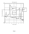
- a characteristic spectrum such as the spectrum of pyrite shown in FIG. 1 .
- the peaks are named for the corresponding original and final shell of the electron that originated the x-ray.
- FIG. 1 shows the sulfur K ⁇ peak, the iron K ⁇ peak and the iron K ⁇ peaks.
- a known solution to reduce this overhead is a dual-beam system consisting of a FIB column and SEM column on the same platform. Each column is optimized for the type of particle beam that it produces. A dual column system is costly because of the two separate focusing columns.
- the SEM of a dual beam system such as the Quanta 3D system from FEI Company, the assignee of the present invention, typically has an imaging resolution of better than five nanometers.
- plasma sources are not typically used for an SEM because the large virtual source size makes for poor resolution compared to other sources.
- electrons are extracted from a plasma source, negative ions are also extracted.
- using the same column for both ions and electrons would result in less than optimum resolution for ions, electrons, or both.
- An object of the invention is to provide a method and apparatus for electron dispersive x-ray spectroscopy analysis of a FIB prepared sample using a single optical column having inductively coupled plasma source.
- a single column inductively coupled plasma source system is outfitted with a power supply and configuration scheme capable of operating in at least two user selectable modes, ion-mode for FIB processing and electron-mode for SEM analysis.
- An attached x-ray detector, spectrometer or other spectrum analyzing system is used to collect the information necessary to determine the physical properties of the sample.
- FIG. 1 shows an example x-ray spectrum of pyrite, which includes iron and sulfur.
- FIG. 2 shows a cross-sectional schematic view of an embodiment of the invention including a portion of an inductively-coupled plasma source with EDS capability.
- FIG. 3 shows a method of one embodiment of the invention in which a sample is prepared in FIB mode then analyzed in SEM mode with EDS.
- FIG. 4 shows a flowchart of an application using a system like the one in FIG. 2 .
- X-rays can escape from a much greater depth and so detectable x-rays continue to be generated as the electron moves downwards and is scattered sideways.
- the "interaction volume,” that is, the region from which signal is detected is much larger for x-rays, typically about a cubic micron, than for secondary electrons.
- the interaction volume not the beam spot size, becomes the critical factor in resolution.
- a preferred embodiment of the invention uses an ICP source equipped with a high voltage bipolar power supply which is capable of selectable modes of operation and sourcing the appropriate voltages for each mode, enabling the generation of a beam of ions or electrons.
- bipolar power supply refers to a power supply capable of switching or reversing polarities of the supplied voltages.
- Power supply means any source of one or more voltages or currents and is not limited to any specific type, form or composition. In an ion mode, the source operates at a high positive potential with respect to ground, and the extractor operates at a high negative voltage with respect to the source voltage.
- the source In electron mode, the source operates at a high negative potential with respect to ground and the extractor operates at high positive potential with respect to the source voltage. It is understood that the different properties of ion and electrons, with the electrons being several orders of magnitude lighter than the ions, requires different operating parameters in the plasma source and in the optical elements in the focusing column. The setting will vary with the type of ion and the application. Based on the guidance provided herein, optimum column settings for a specific application can be readily determined through simulation and routine experimentation. An attached x-ray detector, spectrometer or other spectrum analyzer is used to collect the information necessary to determine the physical properties of the sample.
- FIG. 2 is a schematic diagram of a charged particle beam system 200 of the present invention.
- An RF power supply 222 supplies RF power to a match box 220 which is connected to an antenna 204 which surrounds a source tube 254 within which a plasma is generated.
- a split Faraday shield (not shown) is preferably positioned between the antenna 204 and the interior of the plasma tube 254 to reduce capacitive coupling, thereby reducing the energy spread of the extracted charged particles, reducing chromatic aberration and allowing the particles to be focused to a smaller spot.
- RF power supply 222 could also apply power to the antenna in a "balanced" manner, as described in U.S. Pat. No. 7,241,361 , to further reduce energy spread of the particles in the extracted beam.
- a feed gas to be ionized is fed into the source tube 254 through a feed system 202.
- a biasing power supply 230 is connected to a source biasing electrode 206.
- the source biasing electrode can be biased to a large negative voltage when an electron beam or beam of negative ions is to be generated or to a high positive voltage when a beam of positive ions is to be generated.
- the plasma is typically biased to about positive 30 kV when ions are extract for ion beam milling; the plasma is typically biased to between about negative 20 kV and negative 30 kV when electrons extract for EDS analysis, and the plasma is typically biased to between about negative 1 kV and negative 10 kV when electrons extract for forming a scanning electron beam image.
- Use of an ICP with a split faraday shield and a balanced antenna facilitates the production of a higher resolution beam which is suitable for some application in which a large spot size would not be adequate.
- An extractor electrode 208 in the optical column is biased by a power supply 234, referenced to the output voltage of the biasing power supply 230.
- the power supply 234 is preferably a bipolar power supply so that it can supply either a positive or negative bias to the extractor electrode.
- source biasing electron 208 is preferably a bipolar power supply, capable of applying a positive or negative voltage.
- a condenser electrode 210 in the column is biased by a power supply 232, also referenced to the output voltage of the biasing power supply 230.
- Condenser electrode power supply 232 is preferably bipolar and can bias condenser electrode 210 to a positive or negative bias depending on the charged of particles extracted from the plasma source.
- Ions or electrons are extracted from the plasma contained in the source tube 254 due to the high electric field induced at the lower end of the source tube 254 by the bias voltage on the extractor electrode 208 relative to the voltage on the source biasing electrode 206.
- the ions or electrons extracted from the source tube 254 emerge downwards through the opening in the source biasing electrode 206, forming a charged particle beam which enters the optical column.
- a mass filter 290 typically comprising a deflection in the beam path or a chicane, is used to separate electrons from negative ions that are simultaneously extracted.
- the mass filter 290 is controlled by the mass filter actuator 292.
- the particles could be deflected, for example, by a magnetic deflection element such as a dipole or a quadrupole or by an E x B mass filter.
- the plasma at the lower end of the source tube 254 serves as a "virtual source” of ions or electrons for the charged particle beam column.
- a large portion of the charged particle beam going down the optical column strikes one or more apertures in the column, such as apertures 216, 256, or 214, preferably composed of a material that is resistant to erosion by the ion beam.
- apertures 216, 256, or 214 preferably composed of a material that is resistant to erosion by the ion beam.
- three apertures are shown: 1) an aperture 216 in the source biasing electrode 206, 2) a beam acceptance aperture (BAA) 256, and 3) a beam defining aperture (BDA) 214.
- BAA beam acceptance aperture
- BDA beam defining aperture
- the position of the beam acceptance aperture 256 is controlled by the beam acceptance aperture actuator 236.
- the position and choice of beam defining aperture 214 is controlled by the beam defining aperture actuator 238.
- Two lenses 212 and 242, preferably electrostatic einzel lenses, are shown forming a focused beam 260 on the surface of a sample 240 supported and moved by a sample stage 244 within a vacuum enclosure 246.
- Lenses 212 and 242 are preferably bipolar lenses so that they can act as accelerating lens or decelerating lenses for positively charged or negatively charged particles.
- Lens 212 has a power supply 250, while lens 242 has a power supply 252.
- a pair of deflectors 270 position and move the beam across the work piece surface. Deflectors 270 are controlled by a deflector control 258.
- a pair of x-ray detectors 280 such as solid state silicon drift detectors or Si(Li) detectors collect x-rays to form a spectrum of the work piece.
- a secondary electron detector 282 collects secondary electrons for forming an image by scanning electron microscopy or scanning ion beam imaging.
- System 200 optionally includes other components, such as a gas injector for charged particle beam assisted etching and deposition.
- a controller 284 controls the operation of system 200, and can switch the voltages on the source biasing electrode, on the extractor electrode, and optionally on other components in the system to switch between directing an electron beam toward the work piece or directing an ion beam toward the work piece.
- Embodiments of the invention provide a high current, medium resolution electron beam, which is particularly suited, though not limited, to EDS applications.
- Skilled persons will understand that the operating parameters of the plasma source and the focusing column are typically optimized for the type of particles extracted from the plasma source. Table I shows typical operating parameters for operating with xenon ions, positive oxygen ions, and electrons.
- Skilled persons understand that an einzel lens can be operated as an "acceleration lens” or a "deceleration lens,” depending on the voltage on the lens. In some embodiments, it is preferable to operate the first and second lenses as a accelerating lenses when focusing low energy charged particles and as a decelerating lens when focusing high energy charged particles.
- the electron beam is estimated to have a spot size of less than 80 nm at a beam current of 50 pA, less than 200 nm at a beam current of about 1 nA, less than 1 ⁇ m at a beam current of 100 nA, and less than 2.3 ⁇ m at a beam current of 1 pA.
- spot size is not as small at low beam currents as a convention electron source, considering the interaction volume of one micrometer square for the production of x-rays, the spot size is adequately small for useful EDS analysis, particularly for analyzing sample regions, such as crystal grains, that are typically larger than those spot sizes.
- the brightness of the ICP as an electron source is typically about 6 x 10 4 A/m 2 ⁇ sr ⁇ V.
- FIG. 3 is a flow chart showing a method of one embodiment of the invention in which a sample is prepared in FIB mode then analyzed in SEM mode with EDS.
- the user selects the desired operating mode of the ICP system, ion-mode or electron-mode. For example, if ion-mode is selected, step 304 would follow.
- the appropriate power supplies, gas, and system parameters are setup for FIB operations with the beam voltage source configured with a high positive voltage with respect to ground applied to the source electrode and a high negative voltage with respect to the beam voltage applied to the extractor electrode. With the ion source gas provided and the plasma ignited, an ion beam is generated. Voltages are applied to the focusing lens for focusing the ions.
- the ion beam is directed to the sample for processing.
- the sample is processed by FIB operations which include, for example, imaging, milling, depositing, and analyzing with great precision.
- the user may want to follow-up with SEM imaging and an EDS analysis.
- the user simply switches the ICP operating mode to the electron-mode in step 302.
- the appropriate power supplies, gas, and system parameters are then setup for SEM operations with the beam voltage source configured with a high negative voltage with respect to ground applied to the source electrode and a high positive voltage with respect to the beam voltage applied to the extractor electrode.
- the electron source gas provided and the plasma ignited, an electron beam is generated.
- the electron beam is directed to the sample.
- x-rays are emitted from the surface in response to the impact of the electrons upon the sample and are detected and the energy measured by an energy dispersive x-ray detector.
- step 316 If it is determined in step 316 that not all points in the sample have been scanned, then the electron beam is moved to the next dwell point in step 318, and additional x-rays are collected at that point. The scan continues until the desired portion of the sample surface is completed, with x-rays being collected at each point. After the scan is complete, the x-rays collected while the beam was positioned at each of the scan points are analyzed in step 320, determining which materials are present.
- FIG. 4 shows an application of a system like the one in FIG. 2 .
- a mineral sample is prepared from in an epoxy matrix by known methods. Such samples typically have a 30 mm diameter.
- the sample block is placed in the sample chamber of the charged particle beam system having an ICP charged particle source.
- the sample chamber is evacuated.
- the operating parameters of the plasma source and focusing column are set for an ion beam, such as a beam of xenon ions.
- xenon ions are extracted from the plasma source and directed in a beam toward the sample to remove a small amount of material, such as approximately between 0.1 and 5 microns, from the top surface, depending upon the sample porosity, naturally occurring oxide/nitride thickness, and the grinding method. Because Xenon ions are relatively heavy, they can remove material more rapidly than lighter ions and are less likely to penetrate and remain in the sample.
- the operating parameters of the system are adjusted in step 412 for use with an electron beam.
- the electron beam is scanned across the sample, with x-rays are collected at points on the sample.
- the spectrum collected is analyzed to determine a map of the composition of different points on the sample.
- Removing a material such as a surface layer with the ion beam and then analyzing the exposed material is preferably performed in the same vacuum chamber without exposing the work piece to atmosphere. This provides a clean surface for analysis and prevents the formation of oxides, nitrides, or other compounds that could alter the analysis.
- the ion beam from the plasma source can be used to remove material more rapidly than a LMIS because of the much larger beam current. This is particularly useful in failure analysis of packaged "flip chip" integrated circuits, whose circuitry is exposed from the back side by the ion beam, requiring a great deal of material to be removed.
- the electron beam can them be used to obtain an image and perform a spectroscopic examination of an exposed defect.
- Some embodiments of the invention provide a single charged particle beam column that is switchable between producing an electron beam and producing an ion beam from a single plasma source.
- Some embodiments of the invention use the plasma source as a source of electrons for various operations and analytical techniques. While the embodiments described use the electron beam for EDS analysis, the invention is not limited to any specific use of the electron beam.
- the electron beam could be used for electron beam induced deposition or etching with a suitable precursor gas.
- the electron beam could be used for Auger Electron Spectroscopy, X-ray photoelectron spectroscopy, or wavelength dispersive x-ray spectroscopy.
- the embodiments described above uses an ICP electron source, the invention is not limited to any particular type of plasma electron source and other types of plasma sources, such as a duoplasmatron plasma source, may be useable in some embodiments.
- a charged particle beam system comprises a plasma chamber for maintaining a plasma, a biasing electrode for biasing the plasma to an operating voltage, a power source capable of providing a positive or negative voltage to the biasing electrode, wherein the power source is capable of switching polarity to selectively extract positively or negatively charged particles from the plasma chamber; an extractor electrode for extracting charged particles from the plasma source, an extractor electrode power source capable of providing a positive or negative voltage to the extractor electrode, and a focusing column for focusing the charged particles extracted from the plasma source onto a work piece, wherein the focusing column focuses the positive or negatively charged particles onto the work piece.
- the charged particle beam system further comprises an x-ray detector for detecting x-rays generated by the impact of electrons extracted from the plasma chamber and focused onto the work piece by the focusing column.
- the plasma chamber is part of an inductively coupled plasma source.
- an apparatus for processing and determining properties of a sample comprises an inductively coupled plasma source which selectively operates in a first mode as an ion source and a second mode as an electron source, a power supply configured to selectively provide a first voltage configuration corresponding to the first mode, allowing focused ion beam operations and at least a second voltage configuration corresponding to at least a second mode, allowing SEM operations, and an x-ray detector to collect information necessary to determine a property of a sample.
- the detector is an energy dispersive x-ray detector.
- the energy dispersive x-ray detector is of the silicon drift detector type.
- the property of a sample comprises chemical or elemental composition of the sample.
- the first voltage configuration is comprised of a high positive voltage with respect to ground applied to a source electrode and a high negative voltage with respect to the source electrode voltage applied to an extractor electrode
- the second voltage configuration is comprised of a high negative voltage with respect to ground applied to the source electrode and a high positive voltage with respect to the source electrode voltage applied to the extractor electrode
- a method for processing a sample comprises providing a single column inductively coupled plasma source having user selectable modes of operation such that an ion beam is generated in a first mode and an electron beam is generated in at least a second mode, selecting a mode of operation of the inductively coupled plasma source, directing the generated beam toward a sample, and processing the sample with the generated beam.
- directing the generated beam toward a sample comprises directing a beam having a spot size of less than 200 nm toward the sample. And in accordance with another aspect of some embodiments of the invention, directing the generated beam toward a sample comprises directing the ion beam toward the sample in the first mode and directing the electron beam toward the sample in the second mode.
- processing the sample with the generated beam comprises processing the sample with the ion beam to perform a focused ion beam operation and scanning the sample with the electron beam while collecting emitted x-rays to determining properties of the sample.
- processing the sample with the ion beam to perform a focused ion beam operation includes exposing material for analysis by the electron beam.
- exposing material for analysis by the electron beam includes removing a layer of material from the sample surface.
- a method of processing a sample comprises inductively coupling radio frequency energy from an antenna into a plasma chamber through a split Faraday shield to provide a plasma in the plasma chamber, extracting electrons from the plasma in the plasma chamber, and forming the electrons into a focused beam and directing the beam toward the sample.
- the focused beam of electrons has a spot size at the sample of less than 200 nm with an electron current of 1 nA or greater. And in accordance with another aspect of some embodiments of the invention, the focused beam of electrons has a spot size at the sample of less than 2.3 ⁇ m with an electron current of 1 pA or greater.
- the method further includes detecting emissions from the points impacted by electrons during a scan, and determining properties of the sample from the emissions collected.
- the emissions are x-rays. And in accordance with another aspect of some embodiments of the invention, the emissions are secondary electrons or backscattered electrons.
- the method further comprises extracting ions from the plasma chamber, and forming the ions into a focused beam and directing the beam toward the sample.
- forming the ions into a focused beam and directing the beam toward the sample includes removing material from the sample surface to expose underlying material, and forming the electrons into a focused beam and directing the beam toward the sample includes directing the beam toward the exposed underlying material, without removing the sample from the vacuum chamber.
- extracting ions from the plasma chamber includes extracting argon, xenon, or oxygen ions.
- a method includes extracting ions from the plasma source of an inductively coupled plasma chamber; directing the ions through a focusing column toward the sample to remove material from the sample to expose a surface on the sample; extracting electrons from the plasma source of the inductively coupled plasma chamber; directing the electrons through the focusing column toward the exposed surface on the sample, wherein the inductively coupled plasma source provides the ions in a first user selectable mode of operation to the focusing column that focuses the ions onto the work piece and provides in a second user selectable mode of operation the electrons to the same focusing column to focus the electrons onto the work piece, and detecting emissions generated by the impact of the electrons on the sample to determine a characteristic of the exposed surface.
- Some embodiments include a charged particle beam system, comprising: a plasma chamber for maintaining a plasma; a biasing electrode (206) for electrically biasing the plasma relative to a sample to an operating voltage; a power source (230) capable of providing a positive or negative voltage to the biasing electrode, wherein the power source is capable of switching polarity to selectively extract positively or negatively charged particles from the plasma chamber; an extractor electrode (208) for extracting charged particles from the plasma source; an extractor electrode power source (234) capable of providing a positive or negative voltage to the extractor electrode; a focusing column for focusing the charged particles extracted from the plasma source onto a work piece (240); and a detector (280) for detecting emission from the work piece in the response to the impact of the charged particles on the surface; wherein the power source is capable of switching polarity to selectively extract positively or negatively charged particles from the plasma chamber; the focusing column focuses the positive or negatively charged particles onto the work piece; and the detector detects emissions generated by the impact of electrons extracted from the plasma chamber when the biasing
Abstract
Description
- The present invention relates to charged particle beam systems and, in particular, to the use of an inductively coupled plasma source to provide electrons or ions to process and analyze a sample.
- Focused charged particle beam systems, such as ion and electron beam systems, are used to image, analyze, and modify samples on a microscopic or nanoscopic scale. An electron beam, for example, can be used in a scanning electron microscope (SEM) to form images of a sample by the detection of secondary electrons and for elemental analysis by measuring an x-ray spectrum. A focused ion beam (FIB) system, for example, can be used in a variety of applications in nanotechnology and integrated circuit manufacturing to create and alter microscopic and nanoscopic structures. FIB systems can be used, for example, to image, mill, deposit, and analyze with great precision. Milling or micromachining involves the removal of bulk material at or near the surface of a sample. Milling can be performed without an etch-assisting gas, in a process called sputtering, or using an etch-assisting gas, in a process referred to as chemically-assisted ion beam etching.
U.S. Pat. No. 5,188,705 , which is assigned to the assignee of the present invention, describes a chemically-assisted ion beam etching process. In chemically-assisted ion beam etching, an etch-enhancing gas reacts in the presence of the ion beam to combine with the surface material to form volatile compounds. In FIB deposition, a precursor gas, such as an organometallic compound, decomposes in the presence of the ion beam to deposit material onto the target surface. - The charged particles can be produced from a variety of sources. A "bright" source is desirable because it can produce more charged particles into a smaller spot. The "brightness" of a charged particle beam source is related to the number of charged particles emitted per area and the solid angle into which the particles are emitted. The area from which the particles appear to be emitted is referred to as the "virtual source." High brightness sources typically have small virtual source sizes and can be focused onto smaller spots, which provides for higher resolution processing.
- A liquid metal ion source (LMIS) is very bright and can provide high resolution processing, but is limited to a low beam current at high resolution. A typical system using a gallium LMIS can provide five to seven nanometers of lateral resolution. Such systems are widely used in the characterization and treatment of materials on microscopic to nanoscopic scales. A gallium LMIS comprises a pointed needle coated with a layer of gallium. An electric field is applied to the liquid gallium to extract ions from the source. To produce a very narrow beam for high resolution processing, the current in a beam from an LMIS must be kept relatively low, which means low etch rates and longer processing times. As the beam current is increased beyond a certain point, the resolution rapidly degrades.
- Plasma ion sources ionize gas in a plasma chamber and extract ions to form a beam that is focused on a work piece. Plasma ion sources have larger virtual source sizes than LMISs and are much less bright. An ion beam from a plasma source, therefore, cannot be focused to as small of a spot as the beam from an LMIS, although a plasma source can produce significantly more current. Plasma sources, such as a duoplasmatron source described by Coath and Long, "A High-Brightness Duoplasmatron Ion Source Microprobe Secondary Ion Mass Spectroscopy," Rev. Sci. Instruments 66(2), p. 1018 (1995), have been used as ion sources for ion beam systems, particularly for applications in mass spectroscopy and ion implantation. Inductively coupled plasma (ICP) sources have been used more recently with a focusing column to form a focused beam of charged particles, i.e., ions or electrons.
- An inductively coupled plasma source is capable of providing charged particles within a narrow energy range, which allows the particles to be focused to a smaller spot than ions from a duoplasmatron source. ICP sources, such as the one described in
U.S. Pat. No. 7,241,361 , which is assigned to the assignee of the present invention, include a radio frequency (RF) antenna typically wrapped around a ceramic plasma chamber. The RF antenna provides energy to maintain the gas in an ionized state within the chamber. Because the virtual source size of a plasma source is much larger than the virtual source size of an LMIS, the plasma source is much less bright. - Electron beams are used in a scanning electron microscope (SEM) to form images of a work piece. The electrons are typically provided by a tungsten or lanthanum hexaboride thermionic emitter or a field emission gun, such as a Schottky emitter or a cold cathode emitter. Such emitters provide a small virtual source and can be focused to a very small spot. A typical electron emitter used in an SEM may have a reduced brightness of between about 2 x 10⁷ A/m2·sr·V and 8.2 x 10⁷ A/m2·sr·V. Electrons can be focused to a smaller spot than ions and cause less damage to the sample.
- An electron beam focusing column is significantly different from an ion beam focusing column. For example, electron beam columns typically uses magnetic focusing lenses because of their lower aberration, whereas ion beam columns typically use electrostatic focusing lenses because an excessively large current would be required to focus the heavy ions using a magnetic lens.
- An SEM can be used not only to form an image of a work piece, but also to analyze the processed area for chemical or elemental composition. Energy dispersive spectroscopy (EDS) systems are commonly found on SEMs and are useful in performing localized chemical analysis of a sample. EDS systems utilize the x-ray spectrum emitted by a material impacted by high-energy electrons from the focused beam of electrons of the SEM imaging operation. When an electron impacts the sample, the electron loses energy by a variety of mechanisms. One energy loss mechanism includes transferring the electron energy to an inner shell electron, which can be ejected from the atom as a result. An outer shell electron will then fall into the inner shell, and a characteristic x-ray may be emitted. The energy of the characteristic x-ray is determined by the difference in energies between the inner shell and the outer shell. Because the energies of the shells are characteristic of the element, the energy of the x-ray is also characteristic of the material from which it is emitted. When the number of x-rays at different energies is plotted on a graph, one obtains a characteristic spectrum, such as the spectrum of pyrite shown in
FIG. 1 . The peaks are named for the corresponding original and final shell of the electron that originated the x-ray.FIG. 1 shows the sulfur Kα peak, the iron Kα peak and the iron Kβ peaks. - It is often useful to prepare a sample using a FIB and then use an SEM to image or to perform an EDS analysis. If two separate instruments are used, the user is faced with a lengthy process of removing the sample from the FIB system and then setting up the sample in the EDS capable system which can take upwards of 30 minutes or more. This makes for an unacceptably long time for many applications to be able to analyze a prepared sample.
- A known solution to reduce this overhead is a dual-beam system consisting of a FIB column and SEM column on the same platform. Each column is optimized for the type of particle beam that it produces. A dual column system is costly because of the two separate focusing columns. The SEM of a dual beam system, such as the Quanta 3D system from FEI Company, the assignee of the present invention, typically has an imaging resolution of better than five nanometers.
- While it is known that a plasma chamber can be used as a source of electrons as well as ions, plasma sources are not typically used for an SEM because the large virtual source size makes for poor resolution compared to other sources. Moreover, when electrons are extracted from a plasma source, negative ions are also extracted. Lastly, because the difference in the configuration of the optical columns for focusing electron and focusing ions, using the same column for both ions and electrons would result in less than optimum resolution for ions, electrons, or both.
- An object of the invention is to provide a method and apparatus for electron dispersive x-ray spectroscopy analysis of a FIB prepared sample using a single optical column having inductively coupled plasma source.
- In a preferred embodiment, a single column inductively coupled plasma source system is outfitted with a power supply and configuration scheme capable of operating in at least two user selectable modes, ion-mode for FIB processing and electron-mode for SEM analysis. An attached x-ray detector, spectrometer or other spectrum analyzing system is used to collect the information necessary to determine the physical properties of the sample.
- The foregoing has outlined rather broadly the features and technical advantages of the present invention in order that the detailed description of the invention that follows may be better understood. Additional features and advantages of the invention will be described hereinafter. It should be appreciated by those skilled in the art that the conception and specific embodiments disclosed may be readily utilized as a basis for modifying or designing other structures for carrying out the same purposes of the present invention. It should also be realized by those skilled in the art that such equivalent constructions do not depart from the spirit and scope of the invention as set forth in the appended claims.
- For a more thorough understanding of the present invention, and advantages thereof, reference is now made to the following descriptions taken in conjunction with the accompanying drawings, in which:
-
FIG. 1 shows an example x-ray spectrum of pyrite, which includes iron and sulfur. -
FIG. 2 shows a cross-sectional schematic view of an embodiment of the invention including a portion of an inductively-coupled plasma source with EDS capability. -
FIG. 3 shows a method of one embodiment of the invention in which a sample is prepared in FIB mode then analyzed in SEM mode with EDS. -
FIG. 4 shows a flowchart of an application using a system like the one inFIG. 2 . - While it is known that the resolution of an electron beam from a plasma electron source is poorer than the resolution of an electron beam from a thermionic or field emission source, applicants have recognized that beam resolution is not the limiting factor in many applications, such as EDS. In scanning electron microscopy, secondary electrons used to form the image come from a relatively small interaction volume around the impact point of the primary beam. As the beam electrons penetrate beneath the sample surface, they are scattered randomly away from the beam's point of impact. Only secondary electrons generated near the top surface are capable of escaping and being detected, and those secondary electron typically come from close to the point of impact of the primary beam. X-rays, on the other hand, can escape from a much greater depth and so detectable x-rays continue to be generated as the electron moves downwards and is scattered sideways. Thus, the "interaction volume," that is, the region from which signal is detected, is much larger for x-rays, typically about a cubic micron, than for secondary electrons. For x-rays, the interaction volume, not the beam spot size, becomes the critical factor in resolution. Thus, applicants have found that using a relatively low brightness plasma electron source can provide adequate resolution for EDS, particularly in applications, such as natural resources, in which the sample is relatively uniform over a scale of hundreds of nanometers.
- A preferred embodiment of the invention uses an ICP source equipped with a high voltage bipolar power supply which is capable of selectable modes of operation and sourcing the appropriate voltages for each mode, enabling the generation of a beam of ions or electrons. The term "bipolar power supply" as used herein refers to a power supply capable of switching or reversing polarities of the supplied voltages. "Power supply," as used herein, means any source of one or more voltages or currents and is not limited to any specific type, form or composition. In an ion mode, the source operates at a high positive potential with respect to ground, and the extractor operates at a high negative voltage with respect to the source voltage. In electron mode, the source operates at a high negative potential with respect to ground and the extractor operates at high positive potential with respect to the source voltage. It is understood that the different properties of ion and electrons, with the electrons being several orders of magnitude lighter than the ions, requires different operating parameters in the plasma source and in the optical elements in the focusing column. The setting will vary with the type of ion and the application. Based on the guidance provided herein, optimum column settings for a specific application can be readily determined through simulation and routine experimentation. An attached x-ray detector, spectrometer or other spectrum analyzer is used to collect the information necessary to determine the physical properties of the sample.
-
FIG. 2 is a schematic diagram of a chargedparticle beam system 200 of the present invention. AnRF power supply 222 supplies RF power to amatch box 220 which is connected to anantenna 204 which surrounds asource tube 254 within which a plasma is generated. A split Faraday shield (not shown) is preferably positioned between theantenna 204 and the interior of theplasma tube 254 to reduce capacitive coupling, thereby reducing the energy spread of the extracted charged particles, reducing chromatic aberration and allowing the particles to be focused to a smaller spot.RF power supply 222 could also apply power to the antenna in a "balanced" manner, as described inU.S. Pat. No. 7,241,361 , to further reduce energy spread of the particles in the extracted beam. A feed gas to be ionized is fed into thesource tube 254 through afeed system 202. A biasingpower supply 230 is connected to asource biasing electrode 206. The source biasing electrode can be biased to a large negative voltage when an electron beam or beam of negative ions is to be generated or to a high positive voltage when a beam of positive ions is to be generated. For example, the plasma is typically biased to about positive 30 kV when ions are extract for ion beam milling; the plasma is typically biased to between about negative 20 kV and negative 30 kV when electrons extract for EDS analysis, and the plasma is typically biased to between about negative 1 kV and negative 10 kV when electrons extract for forming a scanning electron beam image. Use of an ICP with a split faraday shield and a balanced antenna facilitates the production of a higher resolution beam which is suitable for some application in which a large spot size would not be adequate. - An extractor electrode 208 in the optical column is biased by a
power supply 234, referenced to the output voltage of the biasingpower supply 230. Thepower supply 234 is preferably a bipolar power supply so that it can supply either a positive or negative bias to the extractor electrode. When electrons or negative ions are being extracted, a voltage positive to the source biasing electron is used; when positive ions are being extracted, a voltage negative to the source biasing electron is used. Thus, source biasing electron 208 is preferably a bipolar power supply, capable of applying a positive or negative voltage. Acondenser electrode 210 in the column is biased by apower supply 232, also referenced to the output voltage of the biasingpower supply 230. Condenserelectrode power supply 232 is preferably bipolar and can biascondenser electrode 210 to a positive or negative bias depending on the charged of particles extracted from the plasma source. - Ions or electrons are extracted from the plasma contained in the
source tube 254 due to the high electric field induced at the lower end of thesource tube 254 by the bias voltage on the extractor electrode 208 relative to the voltage on thesource biasing electrode 206. The ions or electrons extracted from thesource tube 254 emerge downwards through the opening in thesource biasing electrode 206, forming a charged particle beam which enters the optical column. Amass filter 290, typically comprising a deflection in the beam path or a chicane, is used to separate electrons from negative ions that are simultaneously extracted. Themass filter 290 is controlled by themass filter actuator 292. The particles could be deflected, for example, by a magnetic deflection element such as a dipole or a quadrupole or by an E x B mass filter. - Thus, the plasma at the lower end of the
source tube 254 serves as a "virtual source" of ions or electrons for the charged particle beam column. In general, a large portion of the charged particle beam going down the optical column strikes one or more apertures in the column, such asapertures FIG. 2 , three apertures are shown: 1) anaperture 216 in thesource biasing electrode 206, 2) a beam acceptance aperture (BAA) 256, and 3) a beam defining aperture (BDA) 214. - The position of the
beam acceptance aperture 256 is controlled by the beamacceptance aperture actuator 236. The position and choice ofbeam defining aperture 214 is controlled by the beam definingaperture actuator 238. Twolenses focused beam 260 on the surface of asample 240 supported and moved by asample stage 244 within avacuum enclosure 246.Lenses Lens 212 has apower supply 250, whilelens 242 has apower supply 252. - A pair of
deflectors 270 position and move the beam across the work piece surface.Deflectors 270 are controlled by adeflector control 258. A pair ofx-ray detectors 280, such as solid state silicon drift detectors or Si(Li) detectors collect x-rays to form a spectrum of the work piece. Asecondary electron detector 282 collects secondary electrons for forming an image by scanning electron microscopy or scanning ion beam imaging.System 200 optionally includes other components, such as a gas injector for charged particle beam assisted etching and deposition. Acontroller 284 controls the operation ofsystem 200, and can switch the voltages on the source biasing electrode, on the extractor electrode, and optionally on other components in the system to switch between directing an electron beam toward the work piece or directing an ion beam toward the work piece. - Embodiments of the invention provide a high current, medium resolution electron beam, which is particularly suited, though not limited, to EDS applications. Skilled persons will understand that the operating parameters of the plasma source and the focusing column are typically optimized for the type of particles extracted from the plasma source. Table I shows typical operating parameters for operating with xenon ions, positive oxygen ions, and electrons. Skilled persons understand that an einzel lens can be operated as an "acceleration lens" or a "deceleration lens," depending on the voltage on the lens. In some embodiments, it is preferable to operate the first and second lenses as a accelerating lenses when focusing low energy charged particles and as a decelerating lens when focusing high energy charged particles.
Operating parameter Xenon ions Oxygen ions Electrons Gas pressure in plasma chamber .001 mbar to 1.2 mbar .001 mbar to 1.2 mbar .001 mbar to 1.2 mbar Plasma bias voltage + 1 kV to + 30 kV + 1 kV to + 30 kV -1 kV to - 30 kV Extractor electrode voltage (relative to beam voltage) -2 kV to -15 kV -2 kV to -15 kV +2 kV to +15 kV Deflection voltage range -150 V to + 150 V -150 V to + 150 V -150 V to + 150 V First lens voltage 0 V to + 30 kV 0 V to + 30 kV - 30 kV to 0 V Second lens voltage -15 V to + 30 kV -15 V to + 30 kV -30 kV to +15 V RF Power 25 W to 1000 W 25 W to 1000 W 25 W to 1000 W Gas pressure in specimen chamber 5 x 10⁻⁷ mbar to 1 x 10⁻⁷ mbar 5 x 10⁻⁷ mbar to 1 x 10⁻⁷ mbar 5 x 10⁻⁷ mbar to 1 x 10⁻⁷ mbar - Fixed design parameters of the column, such as the position and design of the lenses, is typically optimized for ion beams, although the column design can be optimized for an electron beam or can be a compromise between optimizing for ions and electrons. The electron beam is estimated to have a spot size of less than 80 nm at a beam current of 50 pA, less than 200 nm at a beam current of about 1 nA, less than 1µm at a beam current of 100 nA, and less than 2.3 µm at a beam current of 1 pA. While the spot size is not as small at low beam currents as a convention electron source, considering the interaction volume of one micrometer square for the production of x-rays, the spot size is adequately small for useful EDS analysis, particularly for analyzing sample regions, such as crystal grains, that are typically larger than those spot sizes.
- The brightness of the ICP as an electron source is typically about 6 x 10⁴ A/m2·sr·V.
-
FIG. 3 is a flow chart showing a method of one embodiment of the invention in which a sample is prepared in FIB mode then analyzed in SEM mode with EDS. Instep 302, the user selects the desired operating mode of the ICP system, ion-mode or electron-mode. For example, if ion-mode is selected,step 304 would follow. Instep 304, the appropriate power supplies, gas, and system parameters are setup for FIB operations with the beam voltage source configured with a high positive voltage with respect to ground applied to the source electrode and a high negative voltage with respect to the beam voltage applied to the extractor electrode. With the ion source gas provided and the plasma ignited, an ion beam is generated. Voltages are applied to the focusing lens for focusing the ions. Instep 306, the ion beam is directed to the sample for processing. Instep 308, the sample is processed by FIB operations which include, for example, imaging, milling, depositing, and analyzing with great precision. - Once the sample is FIB processed or prepared, the user may want to follow-up with SEM imaging and an EDS analysis. In such case, the user simply switches the ICP operating mode to the electron-mode in
step 302. Instep 310, the appropriate power supplies, gas, and system parameters are then setup for SEM operations with the beam voltage source configured with a high negative voltage with respect to ground applied to the source electrode and a high positive voltage with respect to the beam voltage applied to the extractor electrode. With the electron source gas provided and the plasma ignited, an electron beam is generated. Instep 312, the electron beam is directed to the sample. Instep 314, x-rays are emitted from the surface in response to the impact of the electrons upon the sample and are detected and the energy measured by an energy dispersive x-ray detector. If it is determined instep 316 that not all points in the sample have been scanned, then the electron beam is moved to the next dwell point instep 318, and additional x-rays are collected at that point. The scan continues until the desired portion of the sample surface is completed, with x-rays being collected at each point. After the scan is complete, the x-rays collected while the beam was positioned at each of the scan points are analyzed instep 320, determining which materials are present. -
FIG. 4 shows an application of a system like the one inFIG. 2 . Instep 402, a mineral sample is prepared from in an epoxy matrix by known methods. Such samples typically have a 30 mm diameter. Instep 404, the sample block is placed in the sample chamber of the charged particle beam system having an ICP charged particle source. Instep 406, the sample chamber is evacuated. Instep 408, the operating parameters of the plasma source and focusing column are set for an ion beam, such as a beam of xenon ions. Instep 410, xenon ions are extracted from the plasma source and directed in a beam toward the sample to remove a small amount of material, such as approximately between 0.1 and 5 microns, from the top surface, depending upon the sample porosity, naturally occurring oxide/nitride thickness, and the grinding method. Because Xenon ions are relatively heavy, they can remove material more rapidly than lighter ions and are less likely to penetrate and remain in the sample. After the top surface of the sample is removed, the operating parameters of the system are adjusted instep 412 for use with an electron beam. Instep 414, the electron beam is scanned across the sample, with x-rays are collected at points on the sample. Instep 416, the spectrum collected is analyzed to determine a map of the composition of different points on the sample. Removing a material such as a surface layer with the ion beam and then analyzing the exposed material is preferably performed in the same vacuum chamber without exposing the work piece to atmosphere. This provides a clean surface for analysis and prevents the formation of oxides, nitrides, or other compounds that could alter the analysis. - In integrated circuit analysis, the ion beam from the plasma source can be used to remove material more rapidly than a LMIS because of the much larger beam current. This is particularly useful in failure analysis of packaged "flip chip" integrated circuits, whose circuitry is exposed from the back side by the ion beam, requiring a great deal of material to be removed. The electron beam can them be used to obtain an image and perform a spectroscopic examination of an exposed defect.
- Some embodiments of the invention provide a single charged particle beam column that is switchable between producing an electron beam and producing an ion beam from a single plasma source. Some embodiments of the invention use the plasma source as a source of electrons for various operations and analytical techniques. While the embodiments described use the electron beam for EDS analysis, the invention is not limited to any specific use of the electron beam. For example, the electron beam could be used for electron beam induced deposition or etching with a suitable precursor gas. The electron beam could be used for Auger Electron Spectroscopy, X-ray photoelectron spectroscopy, or wavelength dispersive x-ray spectroscopy. While the embodiments described above uses an ICP electron source, the invention is not limited to any particular type of plasma electron source and other types of plasma sources, such as a duoplasmatron plasma source, may be useable in some embodiments.
- In accordance with one aspect of some embodiments of the invention, a charged particle beam system comprises a plasma chamber for maintaining a plasma, a biasing electrode for biasing the plasma to an operating voltage, a power source capable of providing a positive or negative voltage to the biasing electrode, wherein the power source is capable of switching polarity to selectively extract positively or negatively charged particles from the plasma chamber; an extractor electrode for extracting charged particles from the plasma source, an extractor electrode power source capable of providing a positive or negative voltage to the extractor electrode, and a focusing column for focusing the charged particles extracted from the plasma source onto a work piece, wherein the focusing column focuses the positive or negatively charged particles onto the work piece.
- In accordance with another aspect of some embodiments of the invention, the charged particle beam system further comprises an x-ray detector for detecting x-rays generated by the impact of electrons extracted from the plasma chamber and focused onto the work piece by the focusing column. And in accordance with another aspect of some embodiments of the invention, the plasma chamber is part of an inductively coupled plasma source.
- In accordance with another aspect of some embodiments of the invention, an apparatus for processing and determining properties of a sample comprises an inductively coupled plasma source which selectively operates in a first mode as an ion source and a second mode as an electron source, a power supply configured to selectively provide a first voltage configuration corresponding to the first mode, allowing focused ion beam operations and at least a second voltage configuration corresponding to at least a second mode, allowing SEM operations, and an x-ray detector to collect information necessary to determine a property of a sample.
- In accordance with another aspect of some embodiments of the invention, the detector is an energy dispersive x-ray detector. And in accordance with another aspect of some embodiments of the invention, the energy dispersive x-ray detector is of the silicon drift detector type.
- In accordance with another aspect of some embodiments of the invention, the property of a sample comprises chemical or elemental composition of the sample.
- In accordance with another aspect of some embodiments of the invention, the first voltage configuration is comprised of a high positive voltage with respect to ground applied to a source electrode and a high negative voltage with respect to the source electrode voltage applied to an extractor electrode, and the second voltage configuration is comprised of a high negative voltage with respect to ground applied to the source electrode and a high positive voltage with respect to the source electrode voltage applied to the extractor electrode.
- In accordance with another aspect of some embodiments of the invention, a method for processing a sample comprises providing a single column inductively coupled plasma source having user selectable modes of operation such that an ion beam is generated in a first mode and an electron beam is generated in at least a second mode, selecting a mode of operation of the inductively coupled plasma source, directing the generated beam toward a sample, and processing the sample with the generated beam.
- In accordance with another aspect of some embodiments of the invention directing the generated beam toward a sample comprises directing a beam having a spot size of less than 200 nm toward the sample. And in accordance with another aspect of some embodiments of the invention, directing the generated beam toward a sample comprises directing the ion beam toward the sample in the first mode and directing the electron beam toward the sample in the second mode.
- In accordance with another aspect of some embodiments of the invention, processing the sample with the generated beam comprises processing the sample with the ion beam to perform a focused ion beam operation and scanning the sample with the electron beam while collecting emitted x-rays to determining properties of the sample. And in accordance with another aspect of some embodiments of the invention, processing the sample with the ion beam to perform a focused ion beam operation includes exposing material for analysis by the electron beam. In accordance with another aspect of some embodiments of the invention, exposing material for analysis by the electron beam includes removing a layer of material from the sample surface.
- In accordance with another aspect of some embodiments of the invention, a method of processing a sample comprises inductively coupling radio frequency energy from an antenna into a plasma chamber through a split Faraday shield to provide a plasma in the plasma chamber, extracting electrons from the plasma in the plasma chamber, and forming the electrons into a focused beam and directing the beam toward the sample.
- In accordance with another aspect of some embodiments of the invention, the focused beam of electrons has a spot size at the sample of less than 200 nm with an electron current of 1 nA or greater. And in accordance with another aspect of some embodiments of the invention, the focused beam of electrons has a spot size at the sample of less than 2.3 µm with an electron current of 1 pA or greater.
- In accordance with another aspect of some embodiments of the invention, the method further includes detecting emissions from the points impacted by electrons during a scan, and determining properties of the sample from the emissions collected.
- In accordance with another aspect of some embodiments of the invention, the emissions are x-rays. And in accordance with another aspect of some embodiments of the invention, the emissions are secondary electrons or backscattered electrons.
- In accordance with another aspect of some embodiments of the invention, the method further comprises extracting ions from the plasma chamber, and forming the ions into a focused beam and directing the beam toward the sample.
- In accordance with another aspect of some embodiments of the invention, forming the ions into a focused beam and directing the beam toward the sample includes removing material from the sample surface to expose underlying material, and forming the electrons into a focused beam and directing the beam toward the sample includes directing the beam toward the exposed underlying material, without removing the sample from the vacuum chamber. And in accordance with another aspect of some embodiments of the invention, extracting ions from the plasma chamber includes extracting argon, xenon, or oxygen ions.
- In some embodiments of the invention, a method includes extracting ions from the plasma source of an inductively coupled plasma chamber; directing the ions through a focusing column toward the sample to remove material from the sample to expose a surface on the sample; extracting electrons from the plasma source of the inductively coupled plasma chamber; directing the electrons through the focusing column toward the exposed surface on the sample, wherein the inductively coupled plasma source provides the ions in a first user selectable mode of operation to the focusing column that focuses the ions onto the work piece and provides in a second user selectable mode of operation the electrons to the same focusing column to focus the electrons onto the work piece, and detecting emissions generated by the impact of the electrons on the sample to determine a characteristic of the exposed surface.
- Some embodiments include a charged particle beam system, comprising: a plasma chamber for maintaining a plasma; a biasing electrode (206) for electrically biasing the plasma relative to a sample to an operating voltage; a power source (230) capable of providing a positive or negative voltage to the biasing electrode, wherein the power source is capable of switching polarity to selectively extract positively or negatively charged particles from the plasma chamber; an extractor electrode (208) for extracting charged particles from the plasma source; an extractor electrode power source (234) capable of providing a positive or negative voltage to the extractor electrode; a focusing column for focusing the charged particles extracted from the plasma source onto a work piece (240); and a detector (280) for detecting emission from the work piece in the response to the impact of the charged particles on the surface; wherein the power source is capable of switching polarity to selectively extract positively or negatively charged particles from the plasma chamber; the focusing column focuses the positive or negatively charged particles onto the work piece; and the detector detects emissions generated by the impact of electrons extracted from the plasma chamber when the biasing electrode is biased negative relative to the sample and focused onto the work piece by the focusing column.
- Although the present invention and its advantages have been described in detail, it should be understood that various changes, substitutions and alterations can be made herein without departing from the spirit and scope of the invention as defined by the appended claims. Moreover, the scope of the present application is not intended to be limited to the particular embodiments of the process, machine, manufacture, composition of matter, means, methods and steps described in the specification. As one of ordinary skill in the art will readily appreciate from the disclosure of the present invention, processes, machines, manufacture, compositions of matter, means, methods, or steps, presently existing or later to be developed that perform substantially the same function or achieve substantially the same result as the corresponding embodiments described herein may be utilized according to the present invention. Accordingly, the appended claims are intended to include within their scope such processes, machines, manufacture, compositions of matter, means, methods, or steps.
Claims (14)
- A method for processing a sample (240), comprising:extracting ions from the plasma source of an inductively coupled plasma chamber;directing the ions through a focusing column toward the sample to remove material from the sample to expose a surface on the sample;extracting electrons from the plasma source of the inductively coupled plasma chamber;directing the electrons through the focusing column toward the exposed surface on the sample;characterized in that the inductively coupled plasma source provides the ions in a first user selectable mode of operation to the focusing column that focuses the ions onto the work piece and provides in a second user selectable mode of operation the electrons to the same focusing column to focus the electrons onto the work piece, anddetecting emissions generated by the impact of the electrons on the sample to determine a characteristic of the exposed surface.
- The method of claim 1 in which detecting emissions generated by the impact of the electrons includes detecting x-rays to determine the composition of the exposed surface.
- The method of claim 1 in which detecting emissions generated by the impact of the electrons includes detecting secondary electrons or backscattered electrons.
- The method of claims 1 - 3 in which plasma from the plasma source is provided by inductively coupling radio frequency energy from an antenna (204) into the inductively coupled plasma chamber through a split Faraday shield.
- The method of claims 1 - 4 in which directing the electrons through the focusing column toward the exposed surface includes directing the electrons through the focusing column toward the exposed surface with a spot size at the sample of less than 200 nm with an electron current of 1 nA or greater.
- The method of claims 1 - 4 in which directing the electrons through the focusing column toward the exposed surface on the sample includes directing the electrons through the focusing column toward the exposed surface with a spot size at the sample of less than 2.3 µm with an electron current of 1 pA or greater.
- The method of claims 1 - 6 in which directing the electrons through the focusing column toward the exposed surface includes directing the electrons through the focusing column toward the exposed surface without removing the sample from the vacuum chamber.
- The method of claim 1 in which extracting ions from the plasma source includes extracting argon, xenon, or oxygen ions.
- A charged particle beam system (200), comprising:a plasma chamber for maintaining a plasma;a biasing electrode (206) for electrically biasing the plasma relative to a sample to an operating voltage;a power source (230) capable of providing a positive or negative voltage to the biasing electrode, wherein the power source is capable of switching polarity to selectively extract positively or negatively charged particles from the plasma chamber;an extractor electrode (208) for extracting charged particles from the plasma source;an extractor electrode power source (234) capable of providing a positive or negative voltage to the extractor electrode;a focusing column for focusing the charged particles extracted from the plasma source onto a work piece (240); anda detector (280) for detecting emission from the work piece in the response to the impact of the charged particles on the surface;characterized in that the power source is capable of switching polarity to selectively extract positively or negatively charged particles from the plasma chamber;the focusing column focuses the positively or negatively charged particles onto the work piece; andthe detector detects emissions generated by the impact of electrons extracted from the plasma chamber when the biasing electrode is biased negative relative to the sample and focused onto the work piece by the focusing column.
- The charged particle beam system of claim 9 in which the detector is an x-ray detector.
- The charged particle beam system of claim 10 in which the x-ray detector is an energy dispersive x-ray detector.
- The charged particle beam system of claim 11 in which the energy dispersive x-ray detector is of the silicon drift detector type.
- The charged particle beam system of claim 9 in which the detector is a backscattered electron detector.
- The charged particle beam system of any of claims 9 - 13 in which:the power supply can be configured to selectively provide a first voltage configuration to allow ion beam operations, the first voltage configuration comprised of a high positive voltage with respect to ground applied to a source electrode and a high negative voltage with respect to the source electrode voltage applied to an extractor electrode; andthe power supply can be configured to selectively provide a second voltage configuration comprised of a high negative voltage with respect to ground applied to the source electrode and a high positive voltage with respect to the source electrode voltage applied to the extractor electrode.
Applications Claiming Priority (1)
| Application Number | Priority Date | Filing Date | Title |
|---|---|---|---|
| US13/306,032 US8716673B2 (en) | 2011-11-29 | 2011-11-29 | Inductively coupled plasma source as an electron beam source for spectroscopic analysis |
Publications (2)
| Publication Number | Publication Date |
|---|---|
| EP2600380A1 true EP2600380A1 (en) | 2013-06-05 |
| EP2600380B1 EP2600380B1 (en) | 2016-04-20 |
Family
ID=47630089
Family Applications (1)
| Application Number | Title | Priority Date | Filing Date |
|---|---|---|---|
| EP12194516.6A Active EP2600380B1 (en) | 2011-11-29 | 2012-11-28 | Inductively coupled plasma source as an electron beam source for spectroscopic analysis |
Country Status (4)
| Country | Link |
|---|---|
| US (3) | US8716673B2 (en) |
| EP (1) | EP2600380B1 (en) |
| JP (1) | JP2013115047A (en) |
| CN (1) | CN103137418B (en) |
Families Citing this family (23)
| Publication number | Priority date | Publication date | Assignee | Title |
|---|---|---|---|---|
| EP2732299A4 (en) | 2011-07-15 | 2015-03-25 | Orbotech Ltd | Electrical inspection of electronic devices using electron-beam induced plasma probes |
| US8716673B2 (en) * | 2011-11-29 | 2014-05-06 | Fei Company | Inductively coupled plasma source as an electron beam source for spectroscopic analysis |
| EP2653891A1 (en) | 2012-04-19 | 2013-10-23 | Fei Company | Method for analyzing an EDS signal |
| WO2013169973A1 (en) * | 2012-05-11 | 2013-11-14 | Ingrain, Inc. | A method and system for multi-energy computer tomographic cuttings analysis |
| US9105438B2 (en) | 2012-05-31 | 2015-08-11 | Fei Company | Imaging and processing for plasma ion source |
| US8664595B2 (en) | 2012-06-28 | 2014-03-04 | Fei Company | Cluster analysis of unknowns in SEM-EDS dataset |
| CN104380425B (en) | 2012-06-29 | 2017-05-31 | Fei 公司 | Multiple types ion gun |
| US9188555B2 (en) | 2012-07-30 | 2015-11-17 | Fei Company | Automated EDS standards calibration |
| US8937282B2 (en) | 2012-10-26 | 2015-01-20 | Fei Company | Mineral identification using mineral definitions including variability |
| US9048067B2 (en) | 2012-10-26 | 2015-06-02 | Fei Company | Mineral identification using sequential decomposition into elements from mineral definitions |
| US9778215B2 (en) | 2012-10-26 | 2017-10-03 | Fei Company | Automated mineral classification |
| US9091635B2 (en) | 2012-10-26 | 2015-07-28 | Fei Company | Mineral identification using mineral definitions having compositional ranges |
| US9194829B2 (en) | 2012-12-28 | 2015-11-24 | Fei Company | Process for performing automated mineralogy |
| US20160299103A1 (en) * | 2013-10-03 | 2016-10-13 | Photon Dynamics Inc. | Application of electron-beam induced plasma probes to inspection, test, debug and surface modifications |
| KR102301793B1 (en) * | 2014-12-18 | 2021-09-14 | 삼성전자주식회사 | Image creating metohd and imaging system for performing the same |
| JP6584787B2 (en) * | 2015-02-13 | 2019-10-02 | 株式会社日立ハイテクノロジーズ | Plasma ion source and charged particle beam device |
| EP3261110A1 (en) * | 2016-06-21 | 2017-12-27 | Excillum AB | X-ray source with ionisation tool |
| US9899181B1 (en) | 2017-01-12 | 2018-02-20 | Fei Company | Collision ionization ion source |
| US9941094B1 (en) | 2017-02-01 | 2018-04-10 | Fei Company | Innovative source assembly for ion beam production |
| CN108878239B (en) * | 2017-05-09 | 2020-07-07 | Fei 公司 | Image processing in charged particle microscope |
| CN111095471B (en) * | 2017-09-18 | 2023-01-24 | Asml荷兰有限公司 | Field programmable detector array |
| JP7094752B2 (en) * | 2018-03-29 | 2022-07-04 | 株式会社ニューフレアテクノロジー | Charged particle beam irradiator |
| US11915908B2 (en) * | 2021-10-14 | 2024-02-27 | Carl Zeiss Smt Gmbh | Method for measuring a sample and microscope implementing the method |
Citations (6)
| Publication number | Priority date | Publication date | Assignee | Title |
|---|---|---|---|---|
| US5188705A (en) | 1991-04-15 | 1993-02-23 | Fei Company | Method of semiconductor device manufacture |
| US20040036032A1 (en) * | 2001-08-31 | 2004-02-26 | Ka-Ngo Leung | Focused electron and ion beam systems |
| US7241361B2 (en) | 2004-02-20 | 2007-07-10 | Fei Company | Magnetically enhanced, inductively coupled plasma source for a focused ion beam system |
| US20100059672A1 (en) * | 2008-09-04 | 2010-03-11 | Ulrike Zeile | Device and method for analyzing a sample |
| EP2312611A2 (en) * | 2009-10-14 | 2011-04-20 | FEI Company | Charged particle beam system having multiple user-selectable operating modes |
| EP2341525A2 (en) * | 2009-12-30 | 2011-07-06 | FEI Company | Plasma source for charged particle beam system |
Family Cites Families (10)
| Publication number | Priority date | Publication date | Assignee | Title |
|---|---|---|---|---|
| JP4067640B2 (en) * | 1998-04-28 | 2008-03-26 | 株式会社ルネサステクノロジ | Charged particle source, charged particle beam apparatus, defect analysis method, and semiconductor device manufacturing method |
| JP3993094B2 (en) * | 2000-07-27 | 2007-10-17 | 株式会社荏原製作所 | Sheet beam inspection system |
| FR2841609B1 (en) * | 2002-06-27 | 2004-09-10 | Snecma Moteurs | BLOWER RETAINER LEVEL RETAINER |
| JP5371142B2 (en) | 2006-07-14 | 2013-12-18 | エフ・イ−・アイ・カンパニー | Multi-source plasma focused ion beam system |
| US7939809B2 (en) * | 2008-05-22 | 2011-05-10 | Vladimir Balakin | Charged particle beam extraction method and apparatus used in conjunction with a charged particle cancer therapy system |
| US8080791B2 (en) | 2008-12-12 | 2011-12-20 | Fei Company | X-ray detector for electron microscope |
| US8124942B2 (en) * | 2010-02-16 | 2012-02-28 | Fei Company | Plasma igniter for an inductively coupled plasma ion source |
| US8633452B2 (en) | 2011-07-13 | 2014-01-21 | Fei Company | Methods and structures for rapid switching between different process gases in an inductively-coupled plasma (ICP) ion source |
| US20130098871A1 (en) * | 2011-10-19 | 2013-04-25 | Fei Company | Internal Split Faraday Shield for an Inductively Coupled Plasma Source |
| US8716673B2 (en) * | 2011-11-29 | 2014-05-06 | Fei Company | Inductively coupled plasma source as an electron beam source for spectroscopic analysis |
-
2011
- 2011-11-29 US US13/306,032 patent/US8716673B2/en active Active
-
2012
- 2012-11-24 JP JP2012256983A patent/JP2013115047A/en active Pending
- 2012-11-28 EP EP12194516.6A patent/EP2600380B1/en active Active
- 2012-11-29 CN CN201210595867.7A patent/CN103137418B/en active Active
-
2014
- 2014-05-06 US US14/271,298 patent/US9275828B2/en active Active
-
2016
- 2016-02-24 US US15/052,650 patent/US9601312B2/en active Active
Patent Citations (6)
| Publication number | Priority date | Publication date | Assignee | Title |
|---|---|---|---|---|
| US5188705A (en) | 1991-04-15 | 1993-02-23 | Fei Company | Method of semiconductor device manufacture |
| US20040036032A1 (en) * | 2001-08-31 | 2004-02-26 | Ka-Ngo Leung | Focused electron and ion beam systems |
| US7241361B2 (en) | 2004-02-20 | 2007-07-10 | Fei Company | Magnetically enhanced, inductively coupled plasma source for a focused ion beam system |
| US20100059672A1 (en) * | 2008-09-04 | 2010-03-11 | Ulrike Zeile | Device and method for analyzing a sample |
| EP2312611A2 (en) * | 2009-10-14 | 2011-04-20 | FEI Company | Charged particle beam system having multiple user-selectable operating modes |
| EP2341525A2 (en) * | 2009-12-30 | 2011-07-06 | FEI Company | Plasma source for charged particle beam system |
Non-Patent Citations (2)
| Title |
|---|
| COATH C D ET AL: "A HIGH-BRIGHTNESS DUOPLASMATRON ION SOURCE FOR MICROPROBE SECONDARY-ION MASS SPECTROMETRY", REVIEW OF SCIENTIFIC INSTRUMENTS, AIP, MELVILLE, NY, US, vol. 66, no. 2, PART 01, 1 February 1995 (1995-02-01), pages 1018 - 1023, XP000503514, ISSN: 0034-6748, DOI: 10.1063/1.1146038 * |
| COATH; LONG: "A High-Brightness Duoplasmatron Ion Source Microprobe Secondary Ion Mass Spectroscopy", REV. SCI. INSTRUMENTS, vol. 66, no. 2, 1995, pages 1018, XP000503514, DOI: doi:10.1063/1.1146038 |
Also Published As
| Publication number | Publication date |
|---|---|
| CN103137418A (en) | 2013-06-05 |
| CN103137418B (en) | 2017-05-24 |
| US8716673B2 (en) | 2014-05-06 |
| US20140326877A1 (en) | 2014-11-06 |
| US20130134307A1 (en) | 2013-05-30 |
| US9275828B2 (en) | 2016-03-01 |
| US9601312B2 (en) | 2017-03-21 |
| US20160172156A1 (en) | 2016-06-16 |
| EP2600380B1 (en) | 2016-04-20 |
| JP2013115047A (en) | 2013-06-10 |
Similar Documents
| Publication | Publication Date | Title |
|---|---|---|
| US9601312B2 (en) | Source for selectively providing positively or negatively charged particles for a focusing column | |
| US10522327B2 (en) | Method of operating a charged particle beam specimen inspection system | |
| US20110163068A1 (en) | Multibeam System | |
| US8835880B2 (en) | Charged particle-beam processing using a cluster source | |
| US7326942B2 (en) | Ion beam system and machining method | |
| JP6118846B2 (en) | Composite focused ion beam apparatus and sample processing method using the same | |
| US8785879B1 (en) | Electron beam wafer inspection system and method of operation thereof | |
| EP2312611A2 (en) | Charged particle beam system having multiple user-selectable operating modes | |
| US9721781B2 (en) | Device for mass spectrometry | |
| US10636615B2 (en) | Composite beam apparatus | |
| EP2787523A1 (en) | Low energy ion milling or deposition | |
| CN107026065B (en) | Charged particle microscope with astigmatism compensation and energy selection | |
| WO2008152132A2 (en) | Apparatus and method for performing secondary ion mass spectroscopy | |
| JPH07296756A (en) | Fine working method, and device therefor | |
| Rauscher | Development of an advanced low energy focused ion beam system based on immersion optics | |
| KR102557373B1 (en) | Focused ion beam impurity identification | |
| US20160042914A1 (en) | Achromatic dual-fib instrument for microfabrication and microanalysis | |
| US20230341341A1 (en) | Particle-induced x-ray emission (pixe) using hydrogen and multi-species focused ion beams | |
| Havelka et al. | S9000X-Next Generation of Ultra-High Resolution SEM for Enhanced Analysis and Xe Plasma FIB for Ultra-Fast and Gentle Sputtering | |
| Bussmann et al. | Stronger field-emission science via coupling novel nanoscale imaging techniques | |
| JP6068553B2 (en) | Ion beam processing / observation apparatus and ion beam processing / observation method using the same | |
| Gnauck et al. | Real Time SEM Imaging of FIB Milling Processes for Extended Accuracy on TEM Samples for EFTEM Analysis |
Legal Events
| Date | Code | Title | Description |
|---|---|---|---|
| PUAI | Public reference made under article 153(3) epc to a published international application that has entered the european phase |
Free format text: ORIGINAL CODE: 0009012 |
|
| AK | Designated contracting states |
Kind code of ref document: A1 Designated state(s): AL AT BE BG CH CY CZ DE DK EE ES FI FR GB GR HR HU IE IS IT LI LT LU LV MC MK MT NL NO PL PT RO RS SE SI SK SM TR |
|
| AX | Request for extension of the european patent |
Extension state: BA ME |
|
| 17P | Request for examination filed |
Effective date: 20131114 |
|
| RBV | Designated contracting states (corrected) |
Designated state(s): AL AT BE BG CH CY CZ DE DK EE ES FI FR GB GR HR HU IE IS IT LI LT LU LV MC MK MT NL NO PL PT RO RS SE SI SK SM TR |
|
| RIC1 | Information provided on ipc code assigned before grant |
Ipc: G01T 1/28 20060101ALI20151104BHEP Ipc: H01J 37/304 20060101ALI20151104BHEP Ipc: H01J 37/26 20060101ALI20151104BHEP Ipc: H01J 37/305 20060101ALI20151104BHEP Ipc: H01J 37/08 20060101AFI20151104BHEP Ipc: H01J 37/30 20060101ALI20151104BHEP Ipc: H01J 27/16 20060101ALI20151104BHEP Ipc: H01J 37/05 20060101ALI20151104BHEP Ipc: H01J 37/077 20060101ALI20151104BHEP |
|
| GRAP | Despatch of communication of intention to grant a patent |
Free format text: ORIGINAL CODE: EPIDOSNIGR1 |
|
| INTG | Intention to grant announced |
Effective date: 20151211 |
|
| GRAS | Grant fee paid |
Free format text: ORIGINAL CODE: EPIDOSNIGR3 |
|
| GRAA | (expected) grant |
Free format text: ORIGINAL CODE: 0009210 |
|
| AK | Designated contracting states |
Kind code of ref document: B1 Designated state(s): AL AT BE BG CH CY CZ DE DK EE ES FI FR GB GR HR HU IE IS IT LI LT LU LV MC MK MT NL NO PL PT RO RS SE SI SK SM TR |
|
| REG | Reference to a national code |
Ref country code: GB Ref legal event code: FG4D |
|
| REG | Reference to a national code |
Ref country code: CH Ref legal event code: EP |
|
| REG | Reference to a national code |
Ref country code: AT Ref legal event code: REF Ref document number: 793248 Country of ref document: AT Kind code of ref document: T Effective date: 20160515 |
|
| REG | Reference to a national code |
Ref country code: IE Ref legal event code: FG4D |
|
| REG | Reference to a national code |
Ref country code: DE Ref legal event code: R096 Ref document number: 602012017265 Country of ref document: DE |
|
| REG | Reference to a national code |
Ref country code: LT Ref legal event code: MG4D |
|
| REG | Reference to a national code |
Ref country code: AT Ref legal event code: MK05 Ref document number: 793248 Country of ref document: AT Kind code of ref document: T Effective date: 20160420 |
|
| REG | Reference to a national code |
Ref country code: NL Ref legal event code: MP Effective date: 20160420 |
|
| PG25 | Lapsed in a contracting state [announced via postgrant information from national office to epo] |
Ref country code: PL Free format text: LAPSE BECAUSE OF FAILURE TO SUBMIT A TRANSLATION OF THE DESCRIPTION OR TO PAY THE FEE WITHIN THE PRESCRIBED TIME-LIMIT Effective date: 20160420 Ref country code: NL Free format text: LAPSE BECAUSE OF FAILURE TO SUBMIT A TRANSLATION OF THE DESCRIPTION OR TO PAY THE FEE WITHIN THE PRESCRIBED TIME-LIMIT Effective date: 20160420 Ref country code: FI Free format text: LAPSE BECAUSE OF FAILURE TO SUBMIT A TRANSLATION OF THE DESCRIPTION OR TO PAY THE FEE WITHIN THE PRESCRIBED TIME-LIMIT Effective date: 20160420 Ref country code: NO Free format text: LAPSE BECAUSE OF FAILURE TO SUBMIT A TRANSLATION OF THE DESCRIPTION OR TO PAY THE FEE WITHIN THE PRESCRIBED TIME-LIMIT Effective date: 20160720 Ref country code: LT Free format text: LAPSE BECAUSE OF FAILURE TO SUBMIT A TRANSLATION OF THE DESCRIPTION OR TO PAY THE FEE WITHIN THE PRESCRIBED TIME-LIMIT Effective date: 20160420 |
|
| PG25 | Lapsed in a contracting state [announced via postgrant information from national office to epo] |
Ref country code: HR Free format text: LAPSE BECAUSE OF FAILURE TO SUBMIT A TRANSLATION OF THE DESCRIPTION OR TO PAY THE FEE WITHIN THE PRESCRIBED TIME-LIMIT Effective date: 20160420 Ref country code: AT Free format text: LAPSE BECAUSE OF FAILURE TO SUBMIT A TRANSLATION OF THE DESCRIPTION OR TO PAY THE FEE WITHIN THE PRESCRIBED TIME-LIMIT Effective date: 20160420 Ref country code: PT Free format text: LAPSE BECAUSE OF FAILURE TO SUBMIT A TRANSLATION OF THE DESCRIPTION OR TO PAY THE FEE WITHIN THE PRESCRIBED TIME-LIMIT Effective date: 20160822 Ref country code: RS Free format text: LAPSE BECAUSE OF FAILURE TO SUBMIT A TRANSLATION OF THE DESCRIPTION OR TO PAY THE FEE WITHIN THE PRESCRIBED TIME-LIMIT Effective date: 20160420 Ref country code: GR Free format text: LAPSE BECAUSE OF FAILURE TO SUBMIT A TRANSLATION OF THE DESCRIPTION OR TO PAY THE FEE WITHIN THE PRESCRIBED TIME-LIMIT Effective date: 20160721 Ref country code: SE Free format text: LAPSE BECAUSE OF FAILURE TO SUBMIT A TRANSLATION OF THE DESCRIPTION OR TO PAY THE FEE WITHIN THE PRESCRIBED TIME-LIMIT Effective date: 20160420 Ref country code: LV Free format text: LAPSE BECAUSE OF FAILURE TO SUBMIT A TRANSLATION OF THE DESCRIPTION OR TO PAY THE FEE WITHIN THE PRESCRIBED TIME-LIMIT Effective date: 20160420 Ref country code: ES Free format text: LAPSE BECAUSE OF FAILURE TO SUBMIT A TRANSLATION OF THE DESCRIPTION OR TO PAY THE FEE WITHIN THE PRESCRIBED TIME-LIMIT Effective date: 20160420 |
|
| PG25 | Lapsed in a contracting state [announced via postgrant information from national office to epo] |
Ref country code: BE Free format text: LAPSE BECAUSE OF FAILURE TO SUBMIT A TRANSLATION OF THE DESCRIPTION OR TO PAY THE FEE WITHIN THE PRESCRIBED TIME-LIMIT Effective date: 20160420 Ref country code: IT Free format text: LAPSE BECAUSE OF FAILURE TO SUBMIT A TRANSLATION OF THE DESCRIPTION OR TO PAY THE FEE WITHIN THE PRESCRIBED TIME-LIMIT Effective date: 20160420 |
|
| REG | Reference to a national code |
Ref country code: DE Ref legal event code: R097 Ref document number: 602012017265 Country of ref document: DE |
|
| REG | Reference to a national code |
Ref country code: FR Ref legal event code: PLFP Year of fee payment: 5 |
|
| PG25 | Lapsed in a contracting state [announced via postgrant information from national office to epo] |
Ref country code: DK Free format text: LAPSE BECAUSE OF FAILURE TO SUBMIT A TRANSLATION OF THE DESCRIPTION OR TO PAY THE FEE WITHIN THE PRESCRIBED TIME-LIMIT Effective date: 20160420 Ref country code: RO Free format text: LAPSE BECAUSE OF FAILURE TO SUBMIT A TRANSLATION OF THE DESCRIPTION OR TO PAY THE FEE WITHIN THE PRESCRIBED TIME-LIMIT Effective date: 20160420 Ref country code: SK Free format text: LAPSE BECAUSE OF FAILURE TO SUBMIT A TRANSLATION OF THE DESCRIPTION OR TO PAY THE FEE WITHIN THE PRESCRIBED TIME-LIMIT Effective date: 20160420 Ref country code: CZ Free format text: LAPSE BECAUSE OF FAILURE TO SUBMIT A TRANSLATION OF THE DESCRIPTION OR TO PAY THE FEE WITHIN THE PRESCRIBED TIME-LIMIT Effective date: 20160420 Ref country code: EE Free format text: LAPSE BECAUSE OF FAILURE TO SUBMIT A TRANSLATION OF THE DESCRIPTION OR TO PAY THE FEE WITHIN THE PRESCRIBED TIME-LIMIT Effective date: 20160420 |
|
| PLBE | No opposition filed within time limit |
Free format text: ORIGINAL CODE: 0009261 |
|
| STAA | Information on the status of an ep patent application or granted ep patent |
Free format text: STATUS: NO OPPOSITION FILED WITHIN TIME LIMIT |
|
| PG25 | Lapsed in a contracting state [announced via postgrant information from national office to epo] |
Ref country code: SM Free format text: LAPSE BECAUSE OF FAILURE TO SUBMIT A TRANSLATION OF THE DESCRIPTION OR TO PAY THE FEE WITHIN THE PRESCRIBED TIME-LIMIT Effective date: 20160420 |
|
| 26N | No opposition filed |
Effective date: 20170123 |
|
| PG25 | Lapsed in a contracting state [announced via postgrant information from national office to epo] |
Ref country code: SI Free format text: LAPSE BECAUSE OF FAILURE TO SUBMIT A TRANSLATION OF THE DESCRIPTION OR TO PAY THE FEE WITHIN THE PRESCRIBED TIME-LIMIT Effective date: 20160420 |
|
| REG | Reference to a national code |
Ref country code: CH Ref legal event code: PL |
|
| PG25 | Lapsed in a contracting state [announced via postgrant information from national office to epo] |
Ref country code: CH Free format text: LAPSE BECAUSE OF NON-PAYMENT OF DUE FEES Effective date: 20161130 Ref country code: LI Free format text: LAPSE BECAUSE OF NON-PAYMENT OF DUE FEES Effective date: 20161130 |
|
| REG | Reference to a national code |
Ref country code: IE Ref legal event code: MM4A |
|
| PG25 | Lapsed in a contracting state [announced via postgrant information from national office to epo] |
Ref country code: LU Free format text: LAPSE BECAUSE OF NON-PAYMENT OF DUE FEES Effective date: 20161130 |
|
| REG | Reference to a national code |
Ref country code: FR Ref legal event code: PLFP Year of fee payment: 6 |
|
| PG25 | Lapsed in a contracting state [announced via postgrant information from national office to epo] |
Ref country code: IE Free format text: LAPSE BECAUSE OF NON-PAYMENT OF DUE FEES Effective date: 20161128 |
|
| PG25 | Lapsed in a contracting state [announced via postgrant information from national office to epo] |
Ref country code: HU Free format text: LAPSE BECAUSE OF FAILURE TO SUBMIT A TRANSLATION OF THE DESCRIPTION OR TO PAY THE FEE WITHIN THE PRESCRIBED TIME-LIMIT; INVALID AB INITIO Effective date: 20121128 Ref country code: CY Free format text: LAPSE BECAUSE OF FAILURE TO SUBMIT A TRANSLATION OF THE DESCRIPTION OR TO PAY THE FEE WITHIN THE PRESCRIBED TIME-LIMIT Effective date: 20160420 |
|
| PG25 | Lapsed in a contracting state [announced via postgrant information from national office to epo] |
Ref country code: MC Free format text: LAPSE BECAUSE OF FAILURE TO SUBMIT A TRANSLATION OF THE DESCRIPTION OR TO PAY THE FEE WITHIN THE PRESCRIBED TIME-LIMIT Effective date: 20160420 Ref country code: TR Free format text: LAPSE BECAUSE OF FAILURE TO SUBMIT A TRANSLATION OF THE DESCRIPTION OR TO PAY THE FEE WITHIN THE PRESCRIBED TIME-LIMIT Effective date: 20160420 Ref country code: MK Free format text: LAPSE BECAUSE OF FAILURE TO SUBMIT A TRANSLATION OF THE DESCRIPTION OR TO PAY THE FEE WITHIN THE PRESCRIBED TIME-LIMIT Effective date: 20160420 Ref country code: IS Free format text: LAPSE BECAUSE OF FAILURE TO SUBMIT A TRANSLATION OF THE DESCRIPTION OR TO PAY THE FEE WITHIN THE PRESCRIBED TIME-LIMIT Effective date: 20160420 |
|
| PG25 | Lapsed in a contracting state [announced via postgrant information from national office to epo] |
Ref country code: BG Free format text: LAPSE BECAUSE OF FAILURE TO SUBMIT A TRANSLATION OF THE DESCRIPTION OR TO PAY THE FEE WITHIN THE PRESCRIBED TIME-LIMIT Effective date: 20160420 |
|
| PG25 | Lapsed in a contracting state [announced via postgrant information from national office to epo] |
Ref country code: MT Free format text: LAPSE BECAUSE OF NON-PAYMENT OF DUE FEES Effective date: 20161128 |
|
| REG | Reference to a national code |
Ref country code: FR Ref legal event code: PLFP Year of fee payment: 7 |
|
| PG25 | Lapsed in a contracting state [announced via postgrant information from national office to epo] |
Ref country code: AL Free format text: LAPSE BECAUSE OF FAILURE TO SUBMIT A TRANSLATION OF THE DESCRIPTION OR TO PAY THE FEE WITHIN THE PRESCRIBED TIME-LIMIT Effective date: 20160420 |
|
| P01 | Opt-out of the competence of the unified patent court (upc) registered |
Effective date: 20230520 |
|
| PGFP | Annual fee paid to national office [announced via postgrant information from national office to epo] |
Ref country code: GB Payment date: 20231128 Year of fee payment: 12 |
|
| PGFP | Annual fee paid to national office [announced via postgrant information from national office to epo] |
Ref country code: FR Payment date: 20231129 Year of fee payment: 12 Ref country code: DE Payment date: 20231116 Year of fee payment: 12 |