EP2600255A2 - Electronic device and method for switching modes of thunderbolt connector thereof - Google Patents
Electronic device and method for switching modes of thunderbolt connector thereof Download PDFInfo
- Publication number
- EP2600255A2 EP2600255A2 EP20120193446 EP12193446A EP2600255A2 EP 2600255 A2 EP2600255 A2 EP 2600255A2 EP 20120193446 EP20120193446 EP 20120193446 EP 12193446 A EP12193446 A EP 12193446A EP 2600255 A2 EP2600255 A2 EP 2600255A2
- Authority
- EP
- European Patent Office
- Prior art keywords
- control unit
- switch circuit
- thunderbolt
- coupled
- thunderbolt control
- Prior art date
- Legal status (The legal status is an assumption and is not a legal conclusion. Google has not performed a legal analysis and makes no representation as to the accuracy of the status listed.)
- Granted
Links
Images





Classifications
-
- G—PHYSICS
- G06—COMPUTING OR CALCULATING; COUNTING
- G06F—ELECTRIC DIGITAL DATA PROCESSING
- G06F13/00—Interconnection of, or transfer of information or other signals between, memories, input/output devices or central processing units
- G06F13/38—Information transfer, e.g. on bus
- G06F13/40—Bus structure
- G06F13/4004—Coupling between buses
- G06F13/4022—Coupling between buses using switching circuits, e.g. switching matrix, connection or expansion network
-
- G—PHYSICS
- G06—COMPUTING OR CALCULATING; COUNTING
- G06F—ELECTRIC DIGITAL DATA PROCESSING
- G06F13/00—Interconnection of, or transfer of information or other signals between, memories, input/output devices or central processing units
- G06F13/38—Information transfer, e.g. on bus
- G06F13/382—Information transfer, e.g. on bus using universal interface adapter
- G06F13/385—Information transfer, e.g. on bus using universal interface adapter for adaptation of a particular data processing system to different peripheral devices
-
- G—PHYSICS
- G06—COMPUTING OR CALCULATING; COUNTING
- G06F—ELECTRIC DIGITAL DATA PROCESSING
- G06F13/00—Interconnection of, or transfer of information or other signals between, memories, input/output devices or central processing units
- G06F13/38—Information transfer, e.g. on bus
- G06F13/40—Bus structure
- G06F13/4063—Device-to-bus coupling
- G06F13/4068—Electrical coupling
-
- G—PHYSICS
- G06—COMPUTING OR CALCULATING; COUNTING
- G06F—ELECTRIC DIGITAL DATA PROCESSING
- G06F2213/00—Indexing scheme relating to interconnection of, or transfer of information or other signals between, memories, input/output devices or central processing units
- G06F2213/0026—PCI express
Definitions
- the invention relates to an electronic device and, more particularly, to a method for switching modes of a thunderbolt connector.
- a conventional electronic device with a thunderbolt connector can only execute one of the host mode and the end-point device mode, and it cannot switch between the host mode and the end-point device mode dynamically.
- the electronic device may be considered as a host or an end-point device via the method for switching modes of the thunderbolt connector.
- the electronic device includes a core unit, a peripheral component interconnection express (PCIE) device, a thunderbolt connecter, a thunderbolt control unit, a first switch circuit and a second switch circuit.
- the core unit includes two PCIE ports.
- the PCIE device includes a PCIE port.
- the thunderbolt connector is coupled to a connecting terminal of the thunderbolt control unit.
- the thunderbolt control unit can be set at a host mode or an end-point device mode dynamically.
- a first common terminal of the first switch circuit is coupled to a PCIE port of the PCIE device, and a first selection terminal of the first switch circuit is coupled to a first PCIE port of the core unit.
- a first common terminal of the second switch circuit is coupled to a first PCIE port of the thunderbolt control unit.
- a first selection terminal of the second switch circuit is coupled to a second PCIE port of the core unit, and a second selection terminal of the second switch circuit is coupled to a second selection terminal of the second switch circuit.
- a method for switching modes of the thunderbolt connector includes providing a thunderbolt control unit.
- the thunderbolt control unit can be set at a host mode or an end-point device mode.
- the thunderbolt control unit is coupled to the core unit of the electronic device and the PCIE device is coupled to the core unit when the thunderbolt control unit is at the host mode.
- the PCIE device is coupled to the thunderbolt control unit when the thunderbolt control unit is at the end-point device mode.
- the electronic device can be both considered as a host and an end-point device by varying the connection among the core unit, the PCIE device and the thunderbolt control unit by switching the first switch circuit and the second circuit.
- FIG.1 is a block diagram showing an electronic device in a first embodiment
- FIG.2 is a block diagram showing an electronic device in a second embodiment
- FIG.3 is a block diagram showing an electronic device in a third embodiment
- FIG.4 is a block diagram showing an electronic device in a fourth embodiment
- FIG.5 is a block diagram showing an electronic device in a fifth embodiment
- FIG.6A and FIG. 6B are block diagrams showing the thunderbolt control unit in FIG.1 ;
- FIG.7 is a block diagram showing an electronic device in a sixth embodiment
- FIG.8 is a block diagram showing an electronic device in a seventh embodiment
- FIG.9 is a flowchart showing a method for switching modes of a thunderbolt connector of an electronic device in a first embodiment
- FIG.10 is a flowchart showing a method for switching modes of a thunderbolt connector of an electronic device in a second embodiment
- FIG.11 is a flowchart showing a method for switching modes of a thunderbolt connector of an electronic device in a third embodiment.
- FIG.12 is a flowchart showing the method for switching modes of a thunderbolt connector of an electronic device in a fourth embodiment.
- FIG.1 is a block diagram showing an electronic device 100 in a first embodiment.
- the electronic device 100 includes a core unit 110, a peripheral component interconnection express (PCIE) device 120, a thunderbolt connector 130, a thunderbolt control unit 140, a first switch circuit 150 and a second switch 160.
- the core unit 110 includes PCIE ports 111 and 112.
- the PCIE device 120 includes a PCIE port 121.
- the PCIE device 120 may be any device connected to a PCIE bus such as a universal serial bus (USB) chip, a wireless local area network (WLAN) chip, and an external serial advanced technology attachment (ESATA) chip.
- USB universal serial bus
- WLAN wireless local area network
- ESATA external serial advanced technology attachment
- the electronic device 100 may be connected to different peripheral devices via different PCIE devices.
- the thunderbolt connector 130 is coupled to a connecting terminal of the thunderbolt control unit 140.
- the thunderbolt control unit 140 is connected to external thunderbolt devices via the thunderbolt connector 130.
- the thunderbolt control unit 140 can be set at a host mode or an end-point device mode dynamically.
- the host mode may be a router mode, which is not limited herein.
- the thunderbolt control unit 140 operates at the host mode, the electronic device 100 is considered as a thunderbolt host.
- the thunderbolt control unit 140 operates at the end-point device mode, the electronic device 100 is considered as an end-point device.
- the first switch circuit 150 and the second switch circuit 160 may be any circuit with the function of connecting and switching signals, such as a Q-switch, a multiplexer, or a switch.
- the first switch circuit 150 can connect a common terminal 151 to one of the selection terminals 152 and 153 selectively.
- the second switch circuit 160 can connect a common terminal 161 to the one of the selection terminals 162 and 163 selectively.
- the common terminal 151 of the first switch circuit 150 is coupled to the PCIE port 121 of the PCIE device 120.
- the selection terminal 152 of the first switch circuit 150 is coupled to the PCIE port 111 of the core unit 110.
- the common terminal 161 of the second switch circuit 160 is coupled to the PCIE port 141 of the thunderbolt control unit 140.
- the selection terminal 162 of the second switch circuit 160 is coupled to the PCIE port 112 of the core unit 110.
- the selection terminal 163 of the second switch circuit 160 is coupled to the selection terminal 153 of the first switch circuit 150.
- the thunderbolt control unit 140 may selectively operate at the host mode or the end-point device mode according to the commands of a user, and it also may be operated at the host mode or the end-point device mode according to whether the core unit 110 is enabled.
- the method for enabling and disabling the core unit 110 may be any method according to the requirements of products. For example, when the core unit 110 operates at a sleep mode (such as the S3 mode), the hibernation mode (such as the S4 mode) or the power off mode or in any other disable mode, the thunderbolt control unit 140 operates at the end-point device mode, which is not limited herein.
- the core unit 110 operates at a normal mode
- the PCIE ports 111 and 112 of the core unit 110 are disabled or turned off. At the moment, although the core unit 110 operates at the normal mode, it is disabled for the thunder control unit 140.
- the thunderbolt control unit 140 may operate at the end-point device mode.
- the thunderbolt control unit 140 may operate at the host mode, which is not limited herein.
- the common terminal 151 of the first switch circuit 150 is coupled to the selection terminal 152 of the first switch circuit 150, and the common terminal 161 of the second switch circuit 160 is coupled to the selection terminal 162 of the second switch circuit 160.
- the PCIE device 120 and the thunderbolt control unit 140 are coupled to the PCIE ports 111 and 112 of the core unit 110 respectively, and the PCIE device 120 is not coupled to the thunderbolt control unit 140. Consequently, the electronic device 100 can be considered as the thunderbolt host, and the core unit 110 can use the PCIE device 120 via the PCIE port 111 and the first switch circuit 150.
- the core unit 110 can also use the external end-point devices (such as a hard disk drive, a display, a network or any other external end-point device) connected to the thunderbolt connector 130 via the PCIE port 112, the second switch circuit 160 and the thunderbolt control unit 140.
- the external end-point devices such as a hard disk drive, a display, a network or any other external end-point device
- the core unit 110 When the thunderbolt control unit 140 operates at the end-point device mode, the core unit 110 may be disabled (such as in the S3 mode, S4 mode, S5 mode or other disable modes) or enabled (or in a normal mode).
- the thunderbolt control unit 140 also may be set to operate at the end-point device mode or the host mode dynamically when the core unit 110 is enabled (or in a normal mode).
- the common terminal 151 of the first switch circuit 150 is coupled to the selection terminal 153 of the first switch circuit 150.
- the common terminal 161 of the second switch circuit 160 is coupled to the selection terminal 163 of the second switch circuit 160. Consequently, the core unit 110 is not coupled to the PCIE device 120 and the thunderbolt control unit 140, and the PCIE device 120 is coupled to the thunderbolt control unit 140. Therefore the electronic device 100 can be used as a thunderbolt end-point device. That is, the external thunderbolt host can use the PCIE device 120 in the electronic device 100 via the thunderbolt connector 130, the thunderbolt control unit 140, the second switch circuit 160 and the first switch circuit 150. Consequently, the user can use electronic devices such as a notebook in the thunderbolt host mode to use the interface and resource connected to the PCIE device 120 via the thunderbolt connector 130 and the thunderbolt control unit 140.
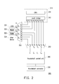
- FIG.2 is a block diagram showing an electronic device 200 in a second embodiment.
- the electronic device 200 includes a core unit 210, PCIE devices 221, 222, 223, 224, a thunderbolt connector 230, a thunderbolt control unit 240, a first switch circuit 250, and a second switch circuit 260.
- the PCIE devices 221 to 224 may be any device connected to the PCIE bus.
- the PCIE device 221 may be a USB host control chip
- the PCIE device 222 may be a WLAN chip
- the PCIE device 223 may be an ESATA chip
- the PCIE device 224 may be any other PCIE device, which is not limited herein
- the core unit 210 includes a central processing unit (CPU) and a south bridge 212.
- the CPU 211 is coupled to the south bridge 212.
- the south bridge 212 includes eight PCIE ports (P1 to P8).
- the first switch circuit 250 includes eight selection terminals (C1 to C8) and four common terminals (X1 to X4).
- the second switch circuit 260 includes eight selection terminals (A1 to A8) and four common terminals (Y1 to Y4).
- the PCIE ports P1 to P4 of the south bridge 212 are coupled to the selection terminals C1 to C4 of the switch circuit 250, respectively.
- the PCIE ports P5 to P8 of the south bridge 212 are coupled to the selection terminal A5 to A8 of the second switch circuit 260, respectively.
- the selection terminals C5 to C8 of the first switch circuit 250 are coupled to the selection terminals A1 to A4 of the second switch circuit 260, respectively.
- the common terminal X1 of the switch circuit 250 is coupled to the PCIE port U1 of the PCIE device 221.
- the common terminal X2 of the first switch circuit 250 is coupled to the PCIE port U2 of the PCIE device 222.
- the common terminal X3 of the switch circuit 250 is coupled to the PCIE port U3 of the PCIE device 223.
- the common terminal X4 of the first switch circuit 250 is coupled to the PCIE port U4 of the PCIE device 224.
- the common terminals Y1 to Y4 of the second switch circuit 250 are coupled to the PCIE ports E1 to E4 of the thunderbolt control unit 220, respectively.
- the common terminals X1 to X4 of the first switch circuit 250 are coupled to the selection terminals C1 to C4 of the first switch circuit 250, respectively, and the common terminals Y1 to Y4 of the second switch circuit 260 are coupled to the selection terminals A5 to A8 of the second switch circuit 260, respectively.
- the CPU (211) 211 of the core unit 210 can use the PCIE devices 221 to 224 via the south bridge 212 and the first switch circuit 250.
- the CPU 211 of the core unit 210 is coupled to the thunderbolt control unit 240 via the south bridge 212 and the second switch circuit 260. Consequently, the CPU (211) 211 can use external thunderbolt devices (such as an external hard disk drive, a display, a network) connected to the thunderbolt port 230 via the thunderbolt control unit 240 in the host mode.
- the core unit 210 When the thunderbolt control unit 240 operates at the end-point device mode, the core unit 210 may be disabled. In another embodiment, when the thunderbolt control unit 240 operates at the end-point device mode, the core unit 210 also may be enabled (or at a normal mode). When the thunderbolt control unit 240 operates at the end-point device mode, the common terminals X1 to X4 of the first switch circuit 250 are coupled to the selection terminals C5 to C8 of the first switch circuit 250 respectively, and the common terminals Y1 to Y4 of the second switch circuit 260 are coupled to the selection terminals A1 to A4 of the second switch circuit 260, respectively.
- the core unit 210 is not coupled to the PCIE devices 221 to 224 and the thunderbolt control unit 240, and the PCIE devices 221 to 224 are coupled to the thunderbolt control unit 240, respectively. Consequently, the external thunderbolt host (such as a notebook) can use the PCIE devices 221 to 224 via the thunderbolt connector 230, the thunderbolt control unit 240, the second switch circuit 260 and the first switch circuit 250.
- the external thunderbolt host such as a notebook
- FIG.3 is a block diagram showing an electronic device 300 in a third embodiment.
- the embodiment shown in FIG.3 can be analogized reference to descriptions about FIG.1 and FIG.2 .
- the electronic device 300 is similar to the electronic device 100, the differences between them are that the core unit 310 of the electronic device 300 includes a CPU 313 and the PCIE device 320 includes a graphics processing unit (GPU) 322.
- the PCIE port 311 of the CPU (211) 313 is coupled to the selection terminal 152 of the first switch circuit 150.
- the CPU 313 is coupled to the selection terminal 162 of the second switch circuit 160 via the PCIE port 312.
- the GPU 322 is coupled to the common terminal 151 of the first circuit 150 via the PCIE port 321.
- the selection terminal 153 of the first switch circuit 150 is coupled to the selection terminal of the second switch circuit 160.
- the GPU 322 and the thunderbolt control unit 140 are coupled to the CPU (211) 313 via the first switch circuit 150 and the second switch circuit 160, respectively.
- the CPU 313 can use the GPU 322 via the first switch circuit 150, which can accelerate the image processing speed and reduce the burden of the CPU (211) 313.
- the CPU 313 can also use the external end-point devices (such as an external hard disk drive, a display, a network) connected to the thunderbolt port 130 via the second switch circuit 160 and the thunderbolt control unit 140.
- the CPU (211) 313 When the thunderbolt control unit 140 operates at the end-point device mode, the CPU (211) 313 is disabled (such as in the S3 mode, S4 mode, S5 mode). In one embodiment, when the thunderbolt control unit 140 operates at the end-point device mode, the CPU (211) mode 313 can also be enabled (or in a normal mode).
- the GPU 322 When the thunderbolt control unit 140 operates at the end-point device mode, the GPU 322 is coupled to the thunderbolt control unit 140 via the first switch circuit 150 and the second switch circuit 160.
- the CPU 313 is not coupled to the GPU 322 and the thunderbolt control unit 140.
- the external thunderbolt host (such as a note book) can use the GPU 322 to process images via the thunderbolt connector 130 and the thunderbolt control unit 140.
- FIG.4 is a block diagram showing an electronic device 400 in a fourth embodiment.
- the embodiment shown in FIG.3 can be analogized reference to descriptions of FIG.1 , FIG.2 and FIG.3 .
- the electronic device 400 is similar to the electronic device 300, the differences between them is that the core unit 410 includes a north bridge 414 except for a CPU 413.
- the north bridge 414 is coupled to the CPU (211) 413.
- the north bridge 414 is coupled to the selection terminal 152 of the first switch circuit via the PCIE port 411.
- the north bridge 414 is coupled to the selection terminal 162 of the second switch circuit 160 via the PCIE port 412.
- the GPU 322 is coupled to the common terminal 151 of the first switch circuit via the PCIE port 321.
- the selection port 153 of the switch circuit 150 is coupled to the selection terminal 163 of the second switch circuit 160.
- the GPU 322 and the thunderbolt control unit 140 are coupled to the PCIE ports 411 and 412 of the north bridge 414 respectively.
- the CPU 413 can use the GPU 322 via the north bridge 414 and the first switch circuit 150, which can accelerate the image processing speed and reduce the burden of the CPU (211) 413.
- the CPU 413 can use the external end-point devices (such as an external hard disk drive, a display, a network) connected to the thunderbolt port 130 via the second switch circuit 160 and the thunderbolt control unit 140.
- the GPU 414 When the thunderbolt control unit 140 operates at the end-point device mode, the GPU 414 is disabled. In one embodiment, when the thunderbolt control unit 140 operates at the end-point device mode, the CPU (211) mode 313 can also be enabled (or in a normal mode). When the thunderbolt control unit 140 operates at the end-point device mode, the south bridge 414 is not coupled to the GPU 322 and the thunderbolt control unit 140, and the GPU 322 is coupled to the thunderbolt control unit 140.
- the external thunderbolt host (such as note book) can use the GPU 322 to process images via the thunderbolt port 130 and the thunderbolt control unit 140.
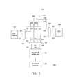
- FIG.5 is a block diagram showing an electronic device 500 in a fifth embodiment.
- the embodiment shown in FIG.3 can be analogized reference to descriptions about FIG.1 and FIG.2 .
- the electronic device 500 includes a core unit 510, a PCIE device 120, a thunderbolt connector 130, a thunderbolt control unit 140, a first switch circuit 150, a second switch circuit 160, a third switch circuit 520 and a GPU 530.
- the core unit 510 includes a south bridge 514 and a CPU 515, and the south bridge 514 is coupled to CPU 515.
- the PCIE port 511 of the south bridge 514 is coupled to the selection terminal 152 of the first switch circuit 150.
- the PCIE port 512 of the south bridge 514 is coupled to the selection terminal 162 of the second switch circuit 160.
- the PCIE port 512 of the south bridge 514 is coupled to selection terminal 166 of the second switch circuit 160.
- the PCIE port 516 of the CPU (211) 515 is coupled to the selection terminal 522 of the third switch circuit 520.
- the common terminal 161 of the second switch circuit 160 is coupled to the PCIE port 141 of the thunderbolt control unit 140.
- the common terminal 165 of the second switch circuit 160 is coupled to the PCIE port 142 of the thunderbolt control unit 140.
- the selection terminal 523 of the third switch circuit 520 is coupled to the selection terminal 164 of the second switch circuit 160.
- the common terminal 521 of the third switch circuit 520 is coupled to the PCIE port 531 of the GPU 530.
- the common terminal 151 of the first switch circuit 150 is coupled to the selection terminal 152 of the first switch circuit 150.
- the common terminal 161 of the second switch circuit 160 is coupled to the selection terminal 162 of the second switch circuit 160.
- the common terminal 165 of the second switch circuit 160 is coupled to the selection terminal 166 of the second switch circuit 160.
- the common terminal 521 of the third switch circuit 520 is coupled to the selection 522 of the third switch circuit 520.
- the CPU 515 is coupled to the PCIE device 120 via the south bridge 514.
- the PCIE device 120 can be a USB control chip, a WLAN chip, an ESATA chip and other PCIE devices.
- the CPU 515 is coupled to the GPU 530 via the PCIE port 516.
- the CPU 515 can use the PCIE device 120 via the south bridge 514, which can improve the image processing ability and reduce the burden of the CPU (211) 515 by using the GPU 530.
- the CPU 515 also may use external end-point devices connected to the thunderbolt port 130 via the south bridge 514, the second switch circuit 160 and the thunderbolt control unit 140.
- the CPU (211) 515 and the south bridge chip 514 When the thunderbolt control unit 140 operates at the end-point device mode, the CPU (211) 515 and the south bridge chip 514 is disabled. In one embodiment, when the thunderbolt control unit 140 operates at the end-point device mode, the CPU (211) 515 and the south bridge chip 514 may also be enabled (or normal mode).
- the common terminal 151 of the first switch circuit 150 is coupled to the selection terminal 153 of the first switch circuit 150.
- the common terminal 161 of the second switch circuit 160 is coupled to the selection terminal 163 of the second switch circuit 160.
- the common terminal 165 of the second switch circuit 160 is coupled to the selection terminal 164 of the second switch circuit 160.
- the common terminal 521 of the third switch circuit 520 is coupled to the selection terminal 523 of the third switch circuit 520.
- the thunderbolt control unit 140 is coupled to the PCIE device 120 via the first switch circuit 150 and the second switch circuit 160, and the thunderbolt control unit 140 is coupled to the GPU 530 via the second switch circuit 160 and the third switch circuit 520.
- the external thunderbolt host (such as note book) can use the PCIE device 120 and the GPU 530 via the thunderbolt port 130 and the thunderbolt control unit 140, and the PCIE device 120 may be a low speed transmission device such as a USB.
- FIG.6A is a block diagram showing the thunderbolt control unit 140 in FIG.1 .
- the thunderbolt control unit 240 in FIG.2 and the thunderbolt control units 140 in FIG.3 to FIG.5 can be analogized reference to descriptions about FIG.6A .
- the thunderbolt control unit 140 includes a memory 143 and a thunderbolt control chip 144.
- the memory 143 may be any kind of memory, such as a non-volatile memory (NVM), a read only memory (ROM), a flash memory, an electrically erasable programmable read-only memory (EEPROM), a programmable read-only memory (PROM), an electrically programmable read-only-memory (EPROM) or any other memory.
- the memory 143 may be a Volatile memory such as a random-access memory (RAM).
- the volatile memory may be supplied via a battery to store data therein.
- the memory 143 includes a host mode firmware 143a and an end-point device mode firmware 143b.
- the thunderbolt control unit 144 is coupled to the common terminal 161 of the second switch circuit 160 via the PCIE port 141.
- the thunderbolt control chip 144 is coupled to the memory 143 and the thunderbolt connector 130.
- the thunderbolt control unit 140 When the thunderbolt control chip executes the host mode firmware 143a, the thunderbolt control unit 140 operates at the host mode. When the thunderbolt control chip 144 executes the end-point mode firmware 143b, the thunderbolt control unit 140 is at the end-point mode. To switch the thunderbolt control unit 140 from the host mode to the end-point device mode, it should reset the thunderbolt control chip 144, and then the thunderbolt control chip 144 executes the end-point device mode firmware 143b. Similarly, to switch the thunderbolt control unit 140 from the end-point device mode to the host mode, it should reset the thunderbolt control chip 144 first, and then the thunderbolt control chip 144 executes the host mode firmware 143a.
- FIG.6B is a block diagram showing a thunderbolt control unit 140 in FIG.1 .
- the thunderbolt control unit 240 of FIG.2 and the thunderbolt control unit 140 of FIG.3 to FIG.5 can be analogized reference to descriptions of FIG.6B .
- the thunderbolt control unit 140 includes a thunderbolt control chip 144, a first memory 145, a second memory 146 and a switch 147.
- the first memory 145 and the second memory 146 may be any kind of memory such as a NVM and a volatile memory.
- the first memory 145 and the second memory 146 may be a ROM, a FLASH memory, an EEPROM, a PROM, an EPROM or any other memory.
- the first memory 145 and the second memory 146 are volatile memories, they may be supplied via a battery to store the data therein.
- the thunderbolt control chip 144 is coupled to the common terminal 161 of the second switch circuit 160 via the PCIE port 141.
- the thunderbolt control chip 144 also may be coupled to the thunderbolt connector 130.
- the first memory 145 includes a host mode firmware 145a.
- the second memory 146 includes an end-point device mode firmware 146a.
- a selection terminal 147a of the switch 147 is coupled to the first memory 145, a selection terminal 147b of the switch 147 is coupled to the second memory 146, and a common terminal 147c of the switch 147 is coupled to the thunderbolt control chip 144.
- the thunderbolt control chip 144 When the common terminal 147c of the switch 147 is coupled to the selection terminal 147a of the switch 147, the thunderbolt control chip 144 is coupled to the first memory 145. Consequently, the thunderbolt control chip 144 reads and executes the Host mode firmware 145a via the switch 147. At the moment, the thunderbolt control unit 140 operates at the Host mode.
- the thunderbolt control chip 144 When the common terminal 147c of the switch 147 is coupled to the selection terminal 147b of the switch 147, the thunderbolt control chip 144 is coupled to the second memory 146. After resetting the thunderbolt control chip 144, the thunderbolt control chip 144 reads and executes the end-point device mode firmware 146a in the second memory 146. At the moment, the thunderbolt control unit 140 operates at the end-point device mode.
- the electronic device in one embodiment includes two thunderbolt control units.
- FIG.7 is a block diagram showing an electronic device 700 in a sixth embodiment, and it can be analogized reference to descriptions about FIG.1 to FIG.5 , FIG.6A, and FIG.6B .
- the electronic device 700 in FIG.7 is similar to the electronic device 200 in FIG.2 , the differences between them are that the electronic device 700 further includes a GPU 530, a third switch circuit 710, and a fourth switch circuit 720, the thunderbolt control unit 240 is replaced by two thunderbolt control units 740 and 770, and the memory 790, and the thunderbolt connector 230 is replaced by two thunderbolt connectors 730 and 780.
- the CPU 211 includes four PCIE ports T1 to T4, and the south bridge 212 includes twelve PCIE ports P1 to P12.
- the thunderbolt control unit 740 includes PCIE ports R1 to R8, and the thunderbolt control unit 770 includes PCIE ports Q1 to Q8.
- the third switch circuit 710 includes selection terminals D1 to D8 and common terminals V1 to V4, the fourth switch circuit 720 includes selection terminals N1 to N8 and common terminals Z1 to Z4, and the GPU 530 includes four PCIE ports G1 to G4.
- the selection terminals D1 to D4 of the third switch circuit 710 are coupled to the PCIE ports T1 to T4 of the CPU (211) 211, respectively.
- the selection terminals D5 to D8 of the third circuit 710 are coupled to the selection terminals N5 to N8 of the fourth switch circuit 720, respectively.
- the common terminals V1 to V4 of the third switch circuit 710 are coupled to the PCIE ports G1 to G4 of the GPU 530, respectively.
- the selection terminals N1 to N4 of the fourth switch circuit 720 are coupled to the PCIE ports P9 to P12 of the south bridge 212, respectively.
- the common terminals Z1 to Z4 of the fourth switch circuit 720 are coupled to the PCIE ports Q1 to Q4 of the thunderbolt control unit 770, respectively.
- the PCIE ports R1 to R4 are coupled to the common terminals Y1 to Y4 of the second switch circuit 260, respectively.
- the thunderbolt control unit 740 is coupled to the thunderbolt control unit 770.
- the thunderbolt control unit 740 is coupled to the thunderbolt control unit 730.
- the thunderbolt control unit 770 is coupled to the thunderbolt connector 780.
- the memory 790 may be any kind of memory such as a non-volatile memory or a volatile memory.
- the memory 143 may be a ROM, a FLASH memory, an EEPROM, a PROM, and an EPROM or any other memory.
- the memory 790 is a volatile memory, and it may be supplied via a battery to keep data stored therein.
- the memory 790 may be analogized reference to descriptions about the memories 145, 146 and the switch 147 in FIG.6B .
- the embodiment of FIG.7 may be analogized reference to descriptions about FIG.2 .
- the thunderbolt control unit 740 is coupled to the memory 790.
- the memory 790 includes a host mode firmware 791 and an end-point device mode firmware 792.
- the thunderbolt control unit 740 reads and executes the host mode firmware 791 of the memory 790, the thunderbolt control unit 740 operates at the host mode.
- the thunderbolt control unit 740 reads and executes the end-point device mode firmware 792 of the memory 790
- the thunderbolt control unit 740 operates at the end-point device mode.
- the thunderbolt control unit 770 is coupled to the memory 760.
- the memory 760 includes a host mode firmware 761 and the end-point device mode firmware 762.
- the thunderbolt control unit 770 may operate at the host mode or the end-point device mode dynamically, which is similar to the method for switching modes of the thunderbolt control unit 740.
- the implementation of the thunderbolt control unit 770 and the memory 760 can be referred to descriptions of the thunderbolt control unit 740 and the memory 790, which is omitted herein.
- the common terminals X1 to X4 of the first switch circuit 250 are coupled to the selection terminals C1 to C4 of the first switch circuit 250, respectively.
- the common terminals Y1 to Y4 of the second switch circuit 260 are coupled to the selection terminals A5 to A8 of the second switch circuit 260, respectively.
- the selection terminals D1 to D4 of the third switch circuit 710 are coupled to the common terminals V1 to V4 of the third switch circuit 710, respectively.
- the selection terminals N1 to N4 of the fourth switch circuit 720 are coupled to the common terminals Z1 to Z4 of the fourth switch circuit 720, respectively.
- the CPU (211) 211 of the core unit 210 can use the PCIE devices 221 to 224 via the south bridge 212 and the first switch circuit 250.
- the CPU 211 can use the GPU 530 via the third switch circuit 710.
- the CPU 211 can use external thunderbolt devices connected to the thunderbolt control unit 730 via the south bridge 212, the second switch circuit 260 and the thunderbolt control unit 740.
- the CPU 211 can use external thunderbolt devices connected to the thunderbolt control connector 780 via the south bridge 212, the fourth switch circuit 720 and the thunderbolt control unit 770.
- the data transmission speed of the electronic device 700 can be accelerated in the host mode.
- the thunderbolt control unit 740 is coupled to the thunderbolt control unit 770, the external thunderbolt devices coupled to the thunderbolt connector 730 can exchange data with the external thunderbolt devices coupled to the thunderbolt connector 780 via the thunderbolt control units 740 and 770 to accelerate the data transmission speed.
- the thunderbolt control units 740 and 770 When the thunderbolt control units 740 and 770 operate at the end- point device mode, one or both of the CPU (211) 211 and the south bridge 212 are disabled. In one embodiment, when the thunderbolt control units 740 and 770 operate at the end-point device mode, the CPU (211) 211 and the south bridge 212 also may be enabled (or in a normal mode).
- the thunderbolt control units 740 and 770 operate at the end-point device mode, the common terminals X1 to X4 of the first switch circuit 250 are coupled to the selection terminals C5 to C8 of the first switch circuit 250 respectively, and the common terminals Y1 to Y4 of the second switch circuit 260 are coupled to the selection terminals A1 to A4 of the second switch circuit 260, respectively.
- the common terminals V1 to V4 of the third switch circuit 710 are coupled to the selection terminals D5 to D8 via the third circuit 710, respectively.
- the common terminals Z1 to Z4 of the fourth switch circuit 720 are coupled to the selection terminals N5 to N8 of the fourth switch circuit 720, respectively. Consequently, the external thunderbolt host (such as a notebook) can use the PCIE devices 221 to 224 via the thunderbolt connector 730, the thunderbolt control unit 740, the second switch circuit 260 and the first switch circuit 250.
- the external thunderbolt host can use the GPU 530 via the thunderbolt connector 780, the thunderbolt control unit 770, the fourth switch circuit 720 and the third switch circuit 710.
- the external thunderbolt host in the end-point device mode can be connected to more PCIE devices, and the external devices coupled to the thunderbolt connectors 730, 780 can exchange data with each other.
- FIG.8 is a block diagram showing an electronic device 800 in a seventh embodiment.
- the electronic device 800 is similar to the electronic device 100, and the difference between them is that electronic device 800 further includes a micro-controller 801.
- the embodiments of FIG.1 to FIG.8 can be analogized reference to related descriptions.
- the micro-controller 801 is coupled to the first circuit 150, the second circuit 160, the core unit 110 and the thunderbolt control unit 140.
- a user can give a mode switching command to the micro-controller 801 via the operation interface.
- the micro-controller 801 controls the thunderbolt control unit 140, the first switch circuit 150 and the second switch circuit 160 according to the switching commands.
- the first switch circuit 150 switches the selection terminal 152 to be coupled to the common terminal 151
- the second switch circuit 160 switches the selection terminal 162 to be coupled to the common terminal 161.
- the micro-controller 801 controls the thunderbolt control unit140 to switch at the host mode.
- the user can give a mode switching command to the micro-controller 801 via the operation interface.
- the micro-controller 801 can control the thunderbolt control unit 140, the first switch circuit 150 and the second switch 160 according to the switching command.
- the selection terminal 153 of the first switch circuit 150 is coupled to the common terminal 151
- the selection terminal 163 of the second switch circuit 160 is coupled to the common terminal 161.
- the micro-controller 801 controls the thunderbolt control unit to switch at the end-point device mode.
- the micro-controller 801 may disable the core unit 110 (such as in the S3 mode, S4 mode, S5 mode or other disable modes). In one embodiment, when the thunderbolt control unit 140 operates at the end-point device mode, the micro-controller 801 controls the core unit 110 to operate at the enable mode.
- the micro-controller 801 also may be used in embodiments shown in FIG. 2 , FIG. 3 , FIG. 4 , FIG. 5 , and FIG. 7 .
- FIG.9 is a flowchart showing the process of the method for switching modes of a thunderbolt connector of the electronic device 100 in a first embodiment.
- step S901 providing a thunderbolt control unit 140 with the host mode and the end-point device mode.
- step S902 determining whether the thunderbolt control unit 140 operates at the host mode. If the thunderbolt control unit 140 operates at the host mode, step S903 is executed, otherwise, step S904 is executed.
- step S903 when the thunderbolt control unit 140 operates at the host mode, the thunderbolt control unit 140 is coupled to the core unit 110 of the electronic device 100, and the PCIE device 120 of the electronic device 100 is coupled to the core unit 110.
- the core unit 110 can use the PCIE device 120 and external end-point devices connected to the thunderbolt connector 130.
- step S904 when the thunderbolt control unit 140 operates at the end-point device mode, the thunderbolt control unit 140 is not coupled to the core unit 110, and the PCIE device 120 is coupled to the thunderbolt control unit 140 but not the core unit 110. Consequently, the external thunderbolt host (such as a notebook) can use the PCIE device 120 via the thunderbolt connector 130 and the thunderbolt control unit 140.
- the thunderbolt control unit 140 operates at the end-point device mode
- FIG.10 is a flowchart showing the process 1000 of the method for switching modes of a thunderbolt connector of an electronic device in a second embodiment. Steps of the flowchart 1000 are similar to steps of the process 900, and the difference between them is that the step S904 is replaced by the step S1004. In contrast with step S904, the step S1004 further includes a step of disabling the core unit 110 when the thunderbolt control unit 140 operates at the end-point device mode.
- FIG.11 is a flowchart showing the process 1100 of the method for switching modes of a thunderbolt of an electronic device in a third embodiment. Steps of the process 1100 are similar to steps of the process 900, the difference between them is that step S1105 is further executed after step S903, and step S 1106 is further executed after step S904.
- step S1105 the thunderbolt control unit 140 executes the host mode firmware of the thunderbolt control unit 140.
- step S 1106 the thunderbolt control unit 140 executes the end-point device mode firmware of the thunderbolt control unit 140.
- step S904 can be replaced by step S1004.
- FIG.12 is a flowchart showing the process 1200 of the method for switching modes of a thunderbolt connector of an electronic device in a fourth embodiment. Steps S901 to S904 in process 1200 is same to those in FIG.9 .
- step S1205 is executed to determine whether the thunderbolt control unit 140 operates at the host mode. That is, whether the Thunderbolt control unit 140 executes the host mode firmware is determined. If the determining result is "YES”, step S1206 is execute to maintain the state, and the thunderbolt control unit 140 continues to execute the host mode firmware. If the determining result is "NO”, step S1207 is executed, the thunderbolt control unit 140 is reset and the thunderbolt control unit 140 executes the host mode firmware.
- step S1205 is executed to determine whether the thunderbolt control unit 140 executes the host mode firmware. If the determining result is "YES”, step S1208 is executed to reset the thunderbolt 140, and the thunderbolt control unit 140 executes the end-point device mode firmware. If the determining result is "NO”, the thunderbolt control unit 140 continues executing the end-point device mode firmware.
- the electronic device and the method for switching modes of a thunderbolt connector can allow the thunderbolt control unit 140 to operate at the host mode or the end-point device mode by switching the connection among the selection terminals and the common terminals of the first switch circuit and the second switch circuit.
- the thunderbolt control unit of the electronic device in the embodiments can be considered as a host to use external end-point devices, and it also can be considered as an end-point device to use the PCIE devices coupled to the thunderbolt control unit.
Landscapes
- Engineering & Computer Science (AREA)
- Theoretical Computer Science (AREA)
- General Engineering & Computer Science (AREA)
- Physics & Mathematics (AREA)
- General Physics & Mathematics (AREA)
- Computer Hardware Design (AREA)
- Mathematical Physics (AREA)
- Information Transfer Systems (AREA)
- Details Of Connecting Devices For Male And Female Coupling (AREA)
Abstract
Description
- The invention relates to an electronic device and, more particularly, to a method for switching modes of a thunderbolt connector.
- A conventional electronic device with a thunderbolt connector can only execute one of the host mode and the end-point device mode, and it cannot switch between the host mode and the end-point device mode dynamically.
- An electronic device and a method for switching modes of a thunderbolt connector are provided. The electronic device may be considered as a host or an end-point device via the method for switching modes of the thunderbolt connector.
- An electronic device is provided. The electronic device includes a core unit, a peripheral component interconnection express (PCIE) device, a thunderbolt connecter, a thunderbolt control unit, a first switch circuit and a second switch circuit. The core unit includes two PCIE ports. The PCIE device includes a PCIE port. The thunderbolt connector is coupled to a connecting terminal of the thunderbolt control unit. The thunderbolt control unit can be set at a host mode or an end-point device mode dynamically. A first common terminal of the first switch circuit is coupled to a PCIE port of the PCIE device, and a first selection terminal of the first switch circuit is coupled to a first PCIE port of the core unit. A first common terminal of the second switch circuit is coupled to a first PCIE port of the thunderbolt control unit. A first selection terminal of the second switch circuit is coupled to a second PCIE port of the core unit, and a second selection terminal of the second switch circuit is coupled to a second selection terminal of the second switch circuit.
- A method for switching modes of the thunderbolt connector is provided. The method includes providing a thunderbolt control unit. The thunderbolt control unit can be set at a host mode or an end-point device mode. The thunderbolt control unit is coupled to the core unit of the electronic device and the PCIE device is coupled to the core unit when the thunderbolt control unit is at the host mode. The PCIE device is coupled to the thunderbolt control unit when the thunderbolt control unit is at the end-point device mode.
- Consequently, the electronic device can be both considered as a host and an end-point device by varying the connection among the core unit, the PCIE device and the thunderbolt control unit by switching the first switch circuit and the second circuit.
- These and other features, aspects and advantages of the present invention will become better understood with regard to the following description, appended claims, and accompanying drawings.
- The accompanying drawings are included to provide a further understanding of the invention, and are incorporated in and constitute a part of this specification. The drawings illustrate embodiments of the invention and, together with the description, serve to explain the principles of the invention.
-
FIG.1 is a block diagram showing an electronic device in a first embodiment; -
FIG.2 is a block diagram showing an electronic device in a second embodiment; -
FIG.3 is a block diagram showing an electronic device in a third embodiment; -
FIG.4 is a block diagram showing an electronic device in a fourth embodiment; -
FIG.5 is a block diagram showing an electronic device in a fifth embodiment; -
FIG.6A and FIG. 6B are block diagrams showing the thunderbolt control unit inFIG.1 ; -
FIG.7 is a block diagram showing an electronic device in a sixth embodiment; -
FIG.8 is a block diagram showing an electronic device in a seventh embodiment; -
FIG.9 is a flowchart showing a method for switching modes of a thunderbolt connector of an electronic device in a first embodiment; -
FIG.10 is a flowchart showing a method for switching modes of a thunderbolt connector of an electronic device in a second embodiment; -
FIG.11 is a flowchart showing a method for switching modes of a thunderbolt connector of an electronic device in a third embodiment; and -
FIG.12 is a flowchart showing the method for switching modes of a thunderbolt connector of an electronic device in a fourth embodiment. - Reference will now be made in detail to the present preferred embodiments of the invention, examples of which are illustrated in the accompanying drawings. Wherever possible, the same reference numbers are used in the drawings and the description to refer to the same or like parts.
-
FIG.1 is a block diagram showing anelectronic device 100 in a first embodiment. Theelectronic device 100 includes acore unit 110, a peripheral component interconnection express (PCIE)device 120, athunderbolt connector 130, athunderbolt control unit 140, afirst switch circuit 150 and asecond switch 160. Thecore unit 110 includesPCIE ports PCIE device 120 includes aPCIE port 121. ThePCIE device 120 may be any device connected to a PCIE bus such as a universal serial bus (USB) chip, a wireless local area network (WLAN) chip, and an external serial advanced technology attachment (ESATA) chip. Theelectronic device 100 may be connected to different peripheral devices via different PCIE devices. - The
thunderbolt connector 130 is coupled to a connecting terminal of thethunderbolt control unit 140. Thethunderbolt control unit 140 is connected to external thunderbolt devices via thethunderbolt connector 130. Thethunderbolt control unit 140 can be set at a host mode or an end-point device mode dynamically. The host mode may be a router mode, which is not limited herein. When thethunderbolt control unit 140 operates at the host mode, theelectronic device 100 is considered as a thunderbolt host. When thethunderbolt control unit 140 operates at the end-point device mode, theelectronic device 100 is considered as an end-point device. - The
first switch circuit 150 and thesecond switch circuit 160 may be any circuit with the function of connecting and switching signals, such as a Q-switch, a multiplexer, or a switch. Thefirst switch circuit 150 can connect acommon terminal 151 to one of theselection terminals second switch circuit 160 can connect acommon terminal 161 to the one of theselection terminals common terminal 151 of thefirst switch circuit 150 is coupled to thePCIE port 121 of thePCIE device 120. Theselection terminal 152 of thefirst switch circuit 150 is coupled to thePCIE port 111 of thecore unit 110. Thecommon terminal 161 of thesecond switch circuit 160 is coupled to thePCIE port 141 of thethunderbolt control unit 140. Theselection terminal 162 of thesecond switch circuit 160 is coupled to thePCIE port 112 of thecore unit 110. Theselection terminal 163 of thesecond switch circuit 160 is coupled to theselection terminal 153 of thefirst switch circuit 150. - The
thunderbolt control unit 140 may selectively operate at the host mode or the end-point device mode according to the commands of a user, and it also may be operated at the host mode or the end-point device mode according to whether thecore unit 110 is enabled. The method for enabling and disabling thecore unit 110 may be any method according to the requirements of products. For example, when thecore unit 110 operates at a sleep mode (such as the S3 mode), the hibernation mode (such as the S4 mode) or the power off mode or in any other disable mode, thethunderbolt control unit 140 operates at the end-point device mode, which is not limited herein. For example, when thecore unit 110 operates at a normal mode, thePCIE ports core unit 110 are disabled or turned off. At the moment, although thecore unit 110 operates at the normal mode, it is disabled for thethunder control unit 140. When thePCIE ports thunderbolt control unit 140 may operate at the end-point device mode. - When the
core unit 110 is at the normal mode (such as the S0 mode or other enable mode), thethunderbolt control unit 140 may operate at the host mode, which is not limited herein. - When the
thunder control unit 140 operates at the host mode, thecommon terminal 151 of thefirst switch circuit 150 is coupled to theselection terminal 152 of thefirst switch circuit 150, and thecommon terminal 161 of thesecond switch circuit 160 is coupled to theselection terminal 162 of thesecond switch circuit 160. ThePCIE device 120 and thethunderbolt control unit 140 are coupled to thePCIE ports core unit 110 respectively, and thePCIE device 120 is not coupled to thethunderbolt control unit 140. Consequently, theelectronic device 100 can be considered as the thunderbolt host, and thecore unit 110 can use thePCIE device 120 via thePCIE port 111 and thefirst switch circuit 150. Thecore unit 110 can also use the external end-point devices (such as a hard disk drive, a display, a network or any other external end-point device) connected to thethunderbolt connector 130 via thePCIE port 112, thesecond switch circuit 160 and thethunderbolt control unit 140. - When the
thunderbolt control unit 140 operates at the end-point device mode, thecore unit 110 may be disabled (such as in the S3 mode, S4 mode, S5 mode or other disable modes) or enabled (or in a normal mode). Thethunderbolt control unit 140 also may be set to operate at the end-point device mode or the host mode dynamically when thecore unit 110 is enabled (or in a normal mode). - The
common terminal 151 of thefirst switch circuit 150 is coupled to theselection terminal 153 of thefirst switch circuit 150. Thecommon terminal 161 of thesecond switch circuit 160 is coupled to theselection terminal 163 of thesecond switch circuit 160. Consequently, thecore unit 110 is not coupled to thePCIE device 120 and thethunderbolt control unit 140, and thePCIE device 120 is coupled to thethunderbolt control unit 140. Therefore theelectronic device 100 can be used as a thunderbolt end-point device. That is, the external thunderbolt host can use thePCIE device 120 in theelectronic device 100 via thethunderbolt connector 130, thethunderbolt control unit 140, thesecond switch circuit 160 and thefirst switch circuit 150. Consequently, the user can use electronic devices such as a notebook in the thunderbolt host mode to use the interface and resource connected to thePCIE device 120 via thethunderbolt connector 130 and thethunderbolt control unit 140. -
FIG.2 is a block diagram showing anelectronic device 200 in a second embodiment. The embodiment shown inFIG.2 can be analogized reference to descriptions aboutFIG.1 . As shown inFIG.2 , theelectronic device 200 includes acore unit 210,PCIE devices thunderbolt connector 230, athunderbolt control unit 240, afirst switch circuit 250, and asecond switch circuit 260. ThePCIE devices 221 to 224 may be any device connected to the PCIE bus. For example, as shown inFIG.2 , thePCIE device 221 may be a USB host control chip, thePCIE device 222 may be a WLAN chip, thePCIE device 223 may be an ESATA chip, and thePCIE device 224 may be any other PCIE device, which is not limited herein - In the embodiment, the
core unit 210 includes a central processing unit (CPU) and asouth bridge 212. TheCPU 211 is coupled to thesouth bridge 212. Thesouth bridge 212 includes eight PCIE ports (P1 to P8). Thefirst switch circuit 250 includes eight selection terminals (C1 to C8) and four common terminals (X1 to X4). Thesecond switch circuit 260 includes eight selection terminals (A1 to A8) and four common terminals (Y1 to Y4). The PCIE ports P1 to P4 of thesouth bridge 212 are coupled to the selection terminals C1 to C4 of theswitch circuit 250, respectively. The PCIE ports P5 to P8 of thesouth bridge 212 are coupled to the selection terminal A5 to A8 of thesecond switch circuit 260, respectively. The selection terminals C5 to C8 of thefirst switch circuit 250 are coupled to the selection terminals A1 to A4 of thesecond switch circuit 260, respectively. The common terminal X1 of theswitch circuit 250 is coupled to the PCIE port U1 of thePCIE device 221. The common terminal X2 of thefirst switch circuit 250 is coupled to the PCIE port U2 of thePCIE device 222. The common terminal X3 of theswitch circuit 250 is coupled to the PCIE port U3 of thePCIE device 223. The common terminal X4 of thefirst switch circuit 250 is coupled to the PCIE port U4 of thePCIE device 224. The common terminals Y1 to Y4 of thesecond switch circuit 250 are coupled to the PCIE ports E1 to E4 of the thunderbolt control unit 220, respectively. - When the
thunderbolt control unit 240 operates at the host mode, the common terminals X1 to X4 of thefirst switch circuit 250 are coupled to the selection terminals C1 to C4 of thefirst switch circuit 250, respectively, and the common terminals Y1 to Y4 of thesecond switch circuit 260 are coupled to the selection terminals A5 to A8 of thesecond switch circuit 260, respectively. As a result, the CPU (211) 211 of thecore unit 210 can use thePCIE devices 221 to 224 via thesouth bridge 212 and thefirst switch circuit 250. TheCPU 211 of thecore unit 210 is coupled to thethunderbolt control unit 240 via thesouth bridge 212 and thesecond switch circuit 260. Consequently, the CPU (211) 211 can use external thunderbolt devices (such as an external hard disk drive, a display, a network) connected to thethunderbolt port 230 via thethunderbolt control unit 240 in the host mode. - When the
thunderbolt control unit 240 operates at the end-point device mode, thecore unit 210 may be disabled. In another embodiment, when thethunderbolt control unit 240 operates at the end-point device mode, thecore unit 210 also may be enabled (or at a normal mode). When thethunderbolt control unit 240 operates at the end-point device mode, the common terminals X1 to X4 of thefirst switch circuit 250 are coupled to the selection terminals C5 to C8 of thefirst switch circuit 250 respectively, and the common terminals Y1 to Y4 of thesecond switch circuit 260 are coupled to the selection terminals A1 to A4 of thesecond switch circuit 260, respectively. Thecore unit 210 is not coupled to thePCIE devices 221 to 224 and thethunderbolt control unit 240, and thePCIE devices 221 to 224 are coupled to thethunderbolt control unit 240, respectively. Consequently, the external thunderbolt host (such as a notebook) can use thePCIE devices 221 to 224 via thethunderbolt connector 230, thethunderbolt control unit 240, thesecond switch circuit 260 and thefirst switch circuit 250. -
FIG.3 is a block diagram showing anelectronic device 300 in a third embodiment. The embodiment shown inFIG.3 can be analogized reference to descriptions aboutFIG.1 andFIG.2 . Theelectronic device 300 is similar to theelectronic device 100, the differences between them are that thecore unit 310 of theelectronic device 300 includes aCPU 313 and thePCIE device 320 includes a graphics processing unit (GPU) 322. ThePCIE port 311 of the CPU (211) 313 is coupled to theselection terminal 152 of thefirst switch circuit 150. TheCPU 313 is coupled to theselection terminal 162 of thesecond switch circuit 160 via thePCIE port 312. TheGPU 322 is coupled to thecommon terminal 151 of thefirst circuit 150 via thePCIE port 321. Theselection terminal 153 of thefirst switch circuit 150 is coupled to the selection terminal of thesecond switch circuit 160. - When the
thunderbolt control unit 140 operates at the host mode, theGPU 322 and thethunderbolt control unit 140 are coupled to the CPU (211) 313 via thefirst switch circuit 150 and thesecond switch circuit 160, respectively. TheCPU 313 can use theGPU 322 via thefirst switch circuit 150, which can accelerate the image processing speed and reduce the burden of the CPU (211) 313. TheCPU 313 can also use the external end-point devices (such as an external hard disk drive, a display, a network) connected to thethunderbolt port 130 via thesecond switch circuit 160 and thethunderbolt control unit 140. - When the
thunderbolt control unit 140 operates at the end-point device mode, the CPU (211) 313 is disabled (such as in the S3 mode, S4 mode, S5 mode). In one embodiment, when thethunderbolt control unit 140 operates at the end-point device mode, the CPU (211)mode 313 can also be enabled (or in a normal mode). When thethunderbolt control unit 140 operates at the end-point device mode, theGPU 322 is coupled to thethunderbolt control unit 140 via thefirst switch circuit 150 and thesecond switch circuit 160. TheCPU 313 is not coupled to theGPU 322 and thethunderbolt control unit 140. The external thunderbolt host (such as a note book) can use theGPU 322 to process images via thethunderbolt connector 130 and thethunderbolt control unit 140. -
FIG.4 is a block diagram showing anelectronic device 400 in a fourth embodiment. The embodiment shown inFIG.3 can be analogized reference to descriptions ofFIG.1 ,FIG.2 andFIG.3 . Theelectronic device 400 is similar to theelectronic device 300, the differences between them is that thecore unit 410 includes anorth bridge 414 except for aCPU 413. Thenorth bridge 414 is coupled to the CPU (211) 413. Thenorth bridge 414 is coupled to theselection terminal 152 of the first switch circuit via thePCIE port 411. Thenorth bridge 414 is coupled to theselection terminal 162 of thesecond switch circuit 160 via thePCIE port 412. TheGPU 322 is coupled to thecommon terminal 151 of the first switch circuit via thePCIE port 321. Theselection port 153 of theswitch circuit 150 is coupled to theselection terminal 163 of thesecond switch circuit 160. - When the
thunderbolt control unit 140 operates at the host mode, theGPU 322 and thethunderbolt control unit 140 are coupled to thePCIE ports north bridge 414 respectively. TheCPU 413 can use theGPU 322 via thenorth bridge 414 and thefirst switch circuit 150, which can accelerate the image processing speed and reduce the burden of the CPU (211) 413. TheCPU 413 can use the external end-point devices (such as an external hard disk drive, a display, a network) connected to thethunderbolt port 130 via thesecond switch circuit 160 and thethunderbolt control unit 140. - When the
thunderbolt control unit 140 operates at the end-point device mode, theGPU 414 is disabled. In one embodiment, when thethunderbolt control unit 140 operates at the end-point device mode, the CPU (211)mode 313 can also be enabled (or in a normal mode). When thethunderbolt control unit 140 operates at the end-point device mode, thesouth bridge 414 is not coupled to theGPU 322 and thethunderbolt control unit 140, and theGPU 322 is coupled to thethunderbolt control unit 140. The external thunderbolt host (such as note book) can use theGPU 322 to process images via thethunderbolt port 130 and thethunderbolt control unit 140. -
FIG.5 is a block diagram showing anelectronic device 500 in a fifth embodiment. The embodiment shown inFIG.3 can be analogized reference to descriptions aboutFIG.1 andFIG.2 . Theelectronic device 500 includes acore unit 510, aPCIE device 120, athunderbolt connector 130, athunderbolt control unit 140, afirst switch circuit 150, asecond switch circuit 160, athird switch circuit 520 and aGPU 530. Thecore unit 510 includes asouth bridge 514 and aCPU 515, and thesouth bridge 514 is coupled toCPU 515. ThePCIE port 511 of thesouth bridge 514 is coupled to theselection terminal 152 of thefirst switch circuit 150. ThePCIE port 512 of thesouth bridge 514 is coupled to theselection terminal 162 of thesecond switch circuit 160. ThePCIE port 512 of thesouth bridge 514 is coupled toselection terminal 166 of thesecond switch circuit 160. ThePCIE port 516 of the CPU (211) 515 is coupled to theselection terminal 522 of thethird switch circuit 520. Thecommon terminal 161 of thesecond switch circuit 160 is coupled to thePCIE port 141 of thethunderbolt control unit 140. Thecommon terminal 165 of thesecond switch circuit 160 is coupled to thePCIE port 142 of thethunderbolt control unit 140. Theselection terminal 523 of thethird switch circuit 520 is coupled to theselection terminal 164 of thesecond switch circuit 160. Thecommon terminal 521 of thethird switch circuit 520 is coupled to thePCIE port 531 of theGPU 530. - When the
thunderbolt control unit 140 operates at the host mode. Thecommon terminal 151 of thefirst switch circuit 150 is coupled to theselection terminal 152 of thefirst switch circuit 150. Thecommon terminal 161 of thesecond switch circuit 160 is coupled to theselection terminal 162 of thesecond switch circuit 160. Thecommon terminal 165 of thesecond switch circuit 160 is coupled to theselection terminal 166 of thesecond switch circuit 160. Thecommon terminal 521 of thethird switch circuit 520 is coupled to theselection 522 of thethird switch circuit 520. TheCPU 515 is coupled to thePCIE device 120 via thesouth bridge 514. ThePCIE device 120 can be a USB control chip, a WLAN chip, an ESATA chip and other PCIE devices. TheCPU 515 is coupled to theGPU 530 via thePCIE port 516. TheCPU 515 can use thePCIE device 120 via thesouth bridge 514, which can improve the image processing ability and reduce the burden of the CPU (211) 515 by using theGPU 530. TheCPU 515 also may use external end-point devices connected to thethunderbolt port 130 via thesouth bridge 514, thesecond switch circuit 160 and thethunderbolt control unit 140. - When the
thunderbolt control unit 140 operates at the end-point device mode, the CPU (211) 515 and thesouth bridge chip 514 is disabled. In one embodiment, when thethunderbolt control unit 140 operates at the end-point device mode, the CPU (211) 515 and thesouth bridge chip 514 may also be enabled (or normal mode). When thethunderbolt control unit 140 operates at the end-point device mode, thecommon terminal 151 of thefirst switch circuit 150 is coupled to theselection terminal 153 of thefirst switch circuit 150. Thecommon terminal 161 of thesecond switch circuit 160 is coupled to theselection terminal 163 of thesecond switch circuit 160. Thecommon terminal 165 of thesecond switch circuit 160 is coupled to theselection terminal 164 of thesecond switch circuit 160. Thecommon terminal 521 of thethird switch circuit 520 is coupled to theselection terminal 523 of thethird switch circuit 520. Thethunderbolt control unit 140 is coupled to thePCIE device 120 via thefirst switch circuit 150 and thesecond switch circuit 160, and thethunderbolt control unit 140 is coupled to theGPU 530 via thesecond switch circuit 160 and thethird switch circuit 520. The external thunderbolt host (such as note book) can use thePCIE device 120 and theGPU 530 via thethunderbolt port 130 and thethunderbolt control unit 140, and thePCIE device 120 may be a low speed transmission device such as a USB. -
FIG.6A is a block diagram showing thethunderbolt control unit 140 inFIG.1 . Thethunderbolt control unit 240 inFIG.2 and thethunderbolt control units 140 inFIG.3 to FIG.5 can be analogized reference to descriptions aboutFIG.6A . As shown inFIG.6A , thethunderbolt control unit 140 includes amemory 143 and athunderbolt control chip 144. Thememory 143 may be any kind of memory, such as a non-volatile memory (NVM), a read only memory (ROM), a flash memory, an electrically erasable programmable read-only memory (EEPROM), a programmable read-only memory (PROM), an electrically programmable read-only-memory (EPROM) or any other memory. In one embodiment, thememory 143 may be a Volatile memory such as a random-access memory (RAM). The volatile memory may be supplied via a battery to store data therein. - The
memory 143 includes ahost mode firmware 143a and an end-pointdevice mode firmware 143b. Thethunderbolt control unit 144 is coupled to thecommon terminal 161 of thesecond switch circuit 160 via thePCIE port 141. Thethunderbolt control chip 144 is coupled to thememory 143 and thethunderbolt connector 130. - When the thunderbolt control chip executes the
host mode firmware 143a, thethunderbolt control unit 140 operates at the host mode. When thethunderbolt control chip 144 executes the end-point mode firmware 143b, thethunderbolt control unit 140 is at the end-point mode. To switch thethunderbolt control unit 140 from the host mode to the end-point device mode, it should reset thethunderbolt control chip 144, and then thethunderbolt control chip 144 executes the end-pointdevice mode firmware 143b. Similarly, to switch thethunderbolt control unit 140 from the end-point device mode to the host mode, it should reset thethunderbolt control chip 144 first, and then thethunderbolt control chip 144 executes thehost mode firmware 143a. -
FIG.6B is a block diagram showing athunderbolt control unit 140 inFIG.1 . Thethunderbolt control unit 240 ofFIG.2 and thethunderbolt control unit 140 ofFIG.3 to FIG.5 can be analogized reference to descriptions ofFIG.6B . As shown inFIG.6B , thethunderbolt control unit 140 includes athunderbolt control chip 144, afirst memory 145, asecond memory 146 and aswitch 147. Thefirst memory 145 and thesecond memory 146 may be any kind of memory such as a NVM and a volatile memory. For example, thefirst memory 145 and thesecond memory 146 may be a ROM, a FLASH memory, an EEPROM, a PROM, an EPROM or any other memory. When thefirst memory 145 and thesecond memory 146 are volatile memories, they may be supplied via a battery to store the data therein. - The
thunderbolt control chip 144 is coupled to thecommon terminal 161 of thesecond switch circuit 160 via thePCIE port 141. Thethunderbolt control chip 144 also may be coupled to thethunderbolt connector 130. Thefirst memory 145 includes ahost mode firmware 145a. Thesecond memory 146 includes an end-pointdevice mode firmware 146a. A selection terminal 147a of theswitch 147 is coupled to thefirst memory 145, aselection terminal 147b of theswitch 147 is coupled to thesecond memory 146, and acommon terminal 147c of theswitch 147 is coupled to thethunderbolt control chip 144. - When the
common terminal 147c of theswitch 147 is coupled to the selection terminal 147a of theswitch 147, thethunderbolt control chip 144 is coupled to thefirst memory 145. Consequently, thethunderbolt control chip 144 reads and executes theHost mode firmware 145a via theswitch 147. At the moment, thethunderbolt control unit 140 operates at the Host mode. - When the
common terminal 147c of theswitch 147 is coupled to theselection terminal 147b of theswitch 147, thethunderbolt control chip 144 is coupled to thesecond memory 146. After resetting thethunderbolt control chip 144, thethunderbolt control chip 144 reads and executes the end-pointdevice mode firmware 146a in thesecond memory 146. At the moment, thethunderbolt control unit 140 operates at the end-point device mode. - The electronic device in one embodiment includes two thunderbolt control units.
-
FIG.7 is a block diagram showing anelectronic device 700 in a sixth embodiment, and it can be analogized reference to descriptions aboutFIG.1 to FIG.5 ,FIG.6A, and FIG.6B . Theelectronic device 700 inFIG.7 is similar to theelectronic device 200 inFIG.2 , the differences between them are that theelectronic device 700 further includes aGPU 530, athird switch circuit 710, and afourth switch circuit 720, thethunderbolt control unit 240 is replaced by twothunderbolt control units memory 790, and thethunderbolt connector 230 is replaced by twothunderbolt connectors CPU 211 includes four PCIE ports T1 to T4, and thesouth bridge 212 includes twelve PCIE ports P1 to P12. Thethunderbolt control unit 740 includes PCIE ports R1 to R8, and thethunderbolt control unit 770 includes PCIE ports Q1 to Q8. Thethird switch circuit 710 includes selection terminals D1 to D8 and common terminals V1 to V4, thefourth switch circuit 720 includes selection terminals N1 to N8 and common terminals Z1 to Z4, and theGPU 530 includes four PCIE ports G1 to G4. - The selection terminals D1 to D4 of the
third switch circuit 710 are coupled to the PCIE ports T1 to T4 of the CPU (211) 211, respectively. The selection terminals D5 to D8 of thethird circuit 710 are coupled to the selection terminals N5 to N8 of thefourth switch circuit 720, respectively. The common terminals V1 to V4 of thethird switch circuit 710 are coupled to the PCIE ports G1 to G4 of theGPU 530, respectively. The selection terminals N1 to N4 of thefourth switch circuit 720 are coupled to the PCIE ports P9 to P12 of thesouth bridge 212, respectively. The common terminals Z1 to Z4 of thefourth switch circuit 720 are coupled to the PCIE ports Q1 to Q4 of thethunderbolt control unit 770, respectively. The PCIE ports R1 to R4 are coupled to the common terminals Y1 to Y4 of thesecond switch circuit 260, respectively. Thethunderbolt control unit 740 is coupled to thethunderbolt control unit 770. Thethunderbolt control unit 740 is coupled to thethunderbolt control unit 730. Thethunderbolt control unit 770 is coupled to thethunderbolt connector 780. - The
memory 790 may be any kind of memory such as a non-volatile memory or a volatile memory. For example, thememory 143 may be a ROM, a FLASH memory, an EEPROM, a PROM, and an EPROM or any other memory. In one embodiment, thememory 790 is a volatile memory, and it may be supplied via a battery to keep data stored therein. In another embodiment, thememory 790 may be analogized reference to descriptions about thememories switch 147 inFIG.6B . - The embodiment of
FIG.7 may be analogized reference to descriptions aboutFIG.2 . Thethunderbolt control unit 740 is coupled to thememory 790. Thememory 790 includes ahost mode firmware 791 and an end-pointdevice mode firmware 792. When thethunderbolt control unit 740 reads and executes thehost mode firmware 791 of thememory 790, thethunderbolt control unit 740 operates at the host mode. When thethunderbolt control unit 740 reads and executes the end-pointdevice mode firmware 792 of thememory 790, thethunderbolt control unit 740 operates at the end-point device mode. Thethunderbolt control unit 770 is coupled to thememory 760. Thememory 760 includes ahost mode firmware 761 and the end-pointdevice mode firmware 762. Thethunderbolt control unit 770 may operate at the host mode or the end-point device mode dynamically, which is similar to the method for switching modes of thethunderbolt control unit 740. The implementation of thethunderbolt control unit 770 and thememory 760 can be referred to descriptions of thethunderbolt control unit 740 and thememory 790, which is omitted herein. - When the
thunderbolt control units first switch circuit 250 are coupled to the selection terminals C1 to C4 of thefirst switch circuit 250, respectively. The common terminals Y1 to Y4 of thesecond switch circuit 260 are coupled to the selection terminals A5 to A8 of thesecond switch circuit 260, respectively. The selection terminals D1 to D4 of thethird switch circuit 710 are coupled to the common terminals V1 to V4 of thethird switch circuit 710, respectively. The selection terminals N1 to N4 of thefourth switch circuit 720 are coupled to the common terminals Z1 to Z4 of thefourth switch circuit 720, respectively. Consequently, the CPU (211) 211 of thecore unit 210 can use thePCIE devices 221 to 224 via thesouth bridge 212 and thefirst switch circuit 250. TheCPU 211 can use theGPU 530 via thethird switch circuit 710. TheCPU 211 can use external thunderbolt devices connected to thethunderbolt control unit 730 via thesouth bridge 212, thesecond switch circuit 260 and the thunderbolt control unit 740.TheCPU 211 can use external thunderbolt devices connected to thethunderbolt control connector 780 via thesouth bridge 212, thefourth switch circuit 720 and thethunderbolt control unit 770. The data transmission speed of theelectronic device 700 can be accelerated in the host mode. Additionally, since thethunderbolt control unit 740 is coupled to thethunderbolt control unit 770, the external thunderbolt devices coupled to thethunderbolt connector 730 can exchange data with the external thunderbolt devices coupled to thethunderbolt connector 780 via thethunderbolt control units - When the
thunderbolt control units south bridge 212 are disabled. In one embodiment, when thethunderbolt control units south bridge 212 also may be enabled (or in a normal mode). When thethunderbolt control units first switch circuit 250 are coupled to the selection terminals C5 to C8 of thefirst switch circuit 250 respectively, and the common terminals Y1 to Y4 of thesecond switch circuit 260 are coupled to the selection terminals A1 to A4 of thesecond switch circuit 260, respectively. The common terminals V1 to V4 of thethird switch circuit 710 are coupled to the selection terminals D5 to D8 via thethird circuit 710, respectively. The common terminals Z1 to Z4 of thefourth switch circuit 720 are coupled to the selection terminals N5 to N8 of thefourth switch circuit 720, respectively. Consequently, the external thunderbolt host (such as a notebook) can use thePCIE devices 221 to 224 via thethunderbolt connector 730, thethunderbolt control unit 740, thesecond switch circuit 260 and thefirst switch circuit 250. The external thunderbolt host can use theGPU 530 via thethunderbolt connector 780, thethunderbolt control unit 770, thefourth switch circuit 720 and thethird switch circuit 710. As a result, the external thunderbolt host in the end-point device mode can be connected to more PCIE devices, and the external devices coupled to thethunderbolt connectors -
FIG.8 is a block diagram showing anelectronic device 800 in a seventh embodiment. Theelectronic device 800 is similar to theelectronic device 100, and the difference between them is thatelectronic device 800 further includes amicro-controller 801. The embodiments ofFIG.1 to FIG.8 can be analogized reference to related descriptions. As shown inFIG.8 , themicro-controller 801 is coupled to thefirst circuit 150, thesecond circuit 160, thecore unit 110 and thethunderbolt control unit 140. - To operate the
electronic device 800 at the host mode, a user can give a mode switching command to themicro-controller 801 via the operation interface. Themicro-controller 801 controls thethunderbolt control unit 140, thefirst switch circuit 150 and thesecond switch circuit 160 according to the switching commands. With the controlling of themicro-controller 801, thefirst switch circuit 150 switches theselection terminal 152 to be coupled to thecommon terminal 151, and thesecond switch circuit 160 switches theselection terminal 162 to be coupled to thecommon terminal 161. Furthermore, themicro-controller 801 controls the thunderbolt control unit140 to switch at the host mode. - To operate the
electronic device 800 at the end-point device mode, the user can give a mode switching command to themicro-controller 801 via the operation interface. Themicro-controller 801 can control thethunderbolt control unit 140, thefirst switch circuit 150 and thesecond switch 160 according to the switching command. With the control of themicro-controller 801, theselection terminal 153 of thefirst switch circuit 150 is coupled to thecommon terminal 151, and theselection terminal 163 of thesecond switch circuit 160 is coupled to thecommon terminal 161. Themicro-controller 801 controls the thunderbolt control unit to switch at the end-point device mode. Themicro-controller 801 may disable the core unit 110 (such as in the S3 mode, S4 mode, S5 mode or other disable modes). In one embodiment, when thethunderbolt control unit 140 operates at the end-point device mode, themicro-controller 801 controls thecore unit 110 to operate at the enable mode. - According to the descriptions of the embodiment, persons having ordinary skills in the art can apply the embodiment to embodiments of
FIG.1 to FIG.7 . For example, themicro-controller 801 also may be used in embodiments shown inFIG. 2 ,FIG. 3 ,FIG. 4 ,FIG. 5 , andFIG. 7 . -
FIG.9 is a flowchart showing the process of the method for switching modes of a thunderbolt connector of theelectronic device 100 in a first embodiment. As shown inFIG.1 andFIG.9 , in step S901, providing athunderbolt control unit 140 with the host mode and the end-point device mode. In step S902, determining whether thethunderbolt control unit 140 operates at the host mode. If thethunderbolt control unit 140 operates at the host mode, step S903 is executed, otherwise, step S904 is executed. - In step S903, when the
thunderbolt control unit 140 operates at the host mode, thethunderbolt control unit 140 is coupled to thecore unit 110 of theelectronic device 100, and thePCIE device 120 of theelectronic device 100 is coupled to thecore unit 110. As a result, thecore unit 110 can use thePCIE device 120 and external end-point devices connected to thethunderbolt connector 130. - In step S904, when the
thunderbolt control unit 140 operates at the end-point device mode, thethunderbolt control unit 140 is not coupled to thecore unit 110, and thePCIE device 120 is coupled to thethunderbolt control unit 140 but not thecore unit 110. Consequently, the external thunderbolt host (such as a notebook) can use thePCIE device 120 via thethunderbolt connector 130 and thethunderbolt control unit 140. -
FIG.10 is a flowchart showing theprocess 1000 of the method for switching modes of a thunderbolt connector of an electronic device in a second embodiment. Steps of theflowchart 1000 are similar to steps of theprocess 900, and the difference between them is that the step S904 is replaced by the step S1004. In contrast with step S904, the step S1004 further includes a step of disabling thecore unit 110 when thethunderbolt control unit 140 operates at the end-point device mode. -
FIG.11 is a flowchart showing theprocess 1100 of the method for switching modes of a thunderbolt of an electronic device in a third embodiment. Steps of theprocess 1100 are similar to steps of theprocess 900, the difference between them is that step S1105 is further executed after step S903, and stepS 1106 is further executed after step S904. In step S1105, thethunderbolt control unit 140 executes the host mode firmware of thethunderbolt control unit 140. Instep S 1106, thethunderbolt control unit 140 executes the end-point device mode firmware of thethunderbolt control unit 140. In another embodiment, step S904 can be replaced by step S1004. -
FIG.12 is a flowchart showing theprocess 1200 of the method for switching modes of a thunderbolt connector of an electronic device in a fourth embodiment. Steps S901 to S904 inprocess 1200 is same to those inFIG.9 . In theprocess 1200, after step S903, step S1205 is executed to determine whether thethunderbolt control unit 140 operates at the host mode. That is, whether theThunderbolt control unit 140 executes the host mode firmware is determined. If the determining result is "YES", step S1206 is execute to maintain the state, and thethunderbolt control unit 140 continues to execute the host mode firmware. If the determining result is "NO", step S1207 is executed, thethunderbolt control unit 140 is reset and thethunderbolt control unit 140 executes the host mode firmware. - After step S904, step S1205 is executed to determine whether the
thunderbolt control unit 140 executes the host mode firmware. If the determining result is "YES", step S1208 is executed to reset thethunderbolt 140, and thethunderbolt control unit 140 executes the end-point device mode firmware. If the determining result is "NO", thethunderbolt control unit 140 continues executing the end-point device mode firmware. - Consequently, the electronic device and the method for switching modes of a thunderbolt connector can allow the
thunderbolt control unit 140 to operate at the host mode or the end-point device mode by switching the connection among the selection terminals and the common terminals of the first switch circuit and the second switch circuit. Unlike conventional thunderbolt controllers, the thunderbolt control unit of the electronic device in the embodiments can be considered as a host to use external end-point devices, and it also can be considered as an end-point device to use the PCIE devices coupled to the thunderbolt control unit. - Although the present invention has been described in considerable detail with reference to certain preferred embodiments thereof, the disclosure is not for limiting the scope of the invention. Persons having ordinary skill in the art may make various modifications and changes without departing from the scope of the invention. Therefore, the scope of the appended claims should not be limited to the description of the preferred embodiments described above.
Claims (15)
- An electronic device (100), characterized by comprising:a core unit (110) including a first peripheral component interconnection express (PCIE) port (111) and a second PCIE port (112);a peripheral device (120) including a PCIE port (121);a thunderbolt connector (130);a thunderbolt control unit (140) coupled to the thunderbolt connector (130), wherein the thunderbolt control unit (140) includes a host mode and an end-point device mode;a first switch circuit (150), wherein, a first common terminal (151) of the first switch circuit (150) is coupled to the PCIE port (121) of the peripheral device (120), and a first selection terminal (152) of the first switch circuit (150) is coupled to the first PCIE port (111) of the core unit (110); anda second switch circuit (160), wherein a first common terminal (161) is coupled to a first PCIE port (141) of the thunderbolt control unit (140), a first selection terminal (162) of the second switch circuit (160) is coupled to the second PCIE port (112) of the core unit (110), and a second selection terminal (163) of the second switch circuit (160) is coupled to a second selection terminal (153) of the first switch circuit (150).
- The electronic device (100) according to claim 1, characterized in that when the thunderbolt control unit (140) operates at the host mode, the first common terminal (151) of the first switch circuit (150) is coupled to the first selection terminal (152) of the first switch circuit (150), the first common terminal (161) of the second switch circuit (160) is coupled to the first selection terminal (162) of the second switch circuit (160); and when the thunderbolt control unit (140) operates at the end-point device mode, the first common terminal (151) of the first switch circuit (150) is coupled to the second selection terminal (153) of the first switch circuit (150), the first common terminal (161) of the second switch circuit (160) is coupled to the second selection terminal (163) of the second switch circuit (160).
- The electronic device (100) according to claim 1, characterized in that the core unit (110) includes a central processing unit (CPU) (211), the peripheral device (120) includes a graphic processing unit (GPU) (322); when the thunderbolt control unit (140) operate at the host mode, the GPU (322) is coupled to the CPU (211) via the first switch circuit (150), the thunderbolt control unit (140) is coupled to the GPU (322) via the second switch circuit (160); and when the thunderbolt control unit (140) operate at the end-point device mode, the GPU (322) is coupled to the thunderbolt control unit (140) via the first switch circuit (150) and second switch circuit (160).
- The electronic device (100) according to claim 1, characterized in that the core unit (110) includes a north bridge (414), and the peripheral device (120) includes a GPU (322); when the thunderbolt control unit (140) operates at the host mode, the GPU (322) is coupled to the north bridge (414) via the first switch circuit (150), the thunderbolt control unit (140) is coupled to the north bridge (414) via the second switch circuit (160); and when the thunderbolt control unit (140) operates at the end-point device mode, the GPU (322) is coupled to the thunderbolt control unit (140) via the first switch circuit (150) and second switch circuit (160).
- The electronic device (100) according to claim 1, characterized in that the core unit (110) includes a south bridge (212), the first selection terminal (152) of the first switch circuit (150) is coupled to the south bridge (212); when the thunderbolt control unit (140) operates at the host mode, the peripheral device (120) is coupled to the south bridge (212) via the first switch circuit (150), and the thunderbolt control unit (140) is coupled to the south bridge (212) via the second switch circuit (160); when the thunderbolt control unit (140) operates at the end-point device mode, the peripheral device (120) is coupled to the thunderbolt control unit (140) via the first switch circuit (150) and the second switch circuit (160).
- The electronic device (100) according to claim 5, characterized in that the core unit (110) further includes a CPU (211), and the electronic device (100) further includes:a GPU (322) including a PCIE port (531); anda third switch circuit (520), wherein a common terminal (161) of the third switch circuit (520) is coupled to the PCIE port (531) of the GPU (322), a first selection terminal (522) of the third switch circuit (520) is coupled to the CPU (211), a second selection terminal (523) of the third switch circuit (520) is coupled to a third selection terminal (164) of the second switch circuit (160);wherein a second common terminal (161) of the second switch circuit (160) is coupled to a second PCIE port (142) of the thunderbolt control unit (140); when the thunderbolt control unit (140) operates at the host mode, the GPU (322) is coupled to the CPU (211) via the third switch circuit (520); and when the thunderbolt control unit (140) operates at the end-point device mode, the GPU (322) is coupled to the thunderbolt control unit (140) via the third switch circuit (520) and the second switch circuit (160).
- The electronic device (100) according to claim 1, characterized in that the thunderbolt control unit (140) includes:a memory (143) storing a host mode firmware (143a) and an end-point device mode firmware (143b); anda thunderbolt control chip (144) is coupled to the first common terminal (161) of the second switch circuit (160) and the memory (143);wherein when the thunderbolt control chip (144) executes the host mode firmware (143a), the thunderbolt control unit (140) operates at the host mode; and when the thunderbolt control chip (144) executes the end-point device mode firmware (143b), the thunderbolt control unit (140) operates at the end-point mode.
- The electronic device (100) according to claim 7, characterized in that the host mode firmware (143a) is executed after the thunderbolt control chip (144) is reset to switch from the end-point device mode to the host mode; and the end-point device mode firmware (143b) is executed after the thunderbolt control chip (144) is reset to switch from the host mode to the end-point device mode.
- The electronic device (100) according to claim 1, characterized in that the thunderbolt control unit (140) includes:a thunderbolt control chip (144) coupled to the first common terminal (161) of the second switch circuit (160);a first memory (145) storing a host mode firmware (145a);a second memory (146) storing an end-point device mode firmware (146a); anda switch 147, wherein a first selection terminal (147a) of the switch (147) is coupled to the first memory (145), a second selection terminal (147b) of the switch (147) is coupled to the second memory (146), and a common terminal (147c) is coupled to the thunderbolt control chip (144);wherein when the thunderbolt control chip (144) reads and executes the host mode firmware (145a) via the switch (147), the thunderbolt control unit (140) operates at the host mode; and when the thunderbolt control chip (144) reads and executes the end-point device mode firmware (146a), the thunderbolt control unit (140) operates at the end-point device mode.
- The electronic device (100) according to claim 1, characterized in that the peripheral device (120) is a universal serial bus (USB) chip, a wireless local area network (WLAN) chip, or an external serial advanced technology attachment (ESATA) chip.
- A method for switching modes of a thunderbolt connector (130) of an electronic device (100), characterized by comprising:providing a thunderbolt control unit (140), wherein the thunderbolt control unit (140) includes a host mode and an end-point device mode;coupling the thunderbolt control unit (140) to a core unit (110) of the electronic device (100) and coupling a peripheral device (120) to the core unit (110) when the thunderbolt control unit (140) operates at the host mode; andcoupling the peripheral device (120) to the thunderbolt control unit (140) when the thunderbolt control unit (140) operates at the end-point device mode.
- The method for switching modes of the thunderbolt connector (130) of the electronic device (100) according to claim 11, characterized in that the core unit (110) is disabled when the thunderbolt control unit (140) operates at the end-point device mode.
- The method for switching modes of the thunderbolt connector (130) of the electronic device (100) according to claim 11, characterized by further comprising that the thunderbolt control unit (140) operates at the host mode when the thunderbolt control unit (140) executes the host mode firmware (143a); and the thunderbolt control unit (140) operates at the end-device mode when the thunderbolt control unit (140) executes the end-point device mode firmware (143b).
- The method for switching modes of the thunderbolt connector (130) of the electronic device (100) according to claim 13, characterized by further comprising:resetting the thunderbolt control unit (140) and executing the host mode firmware (143a) via the thunderbolt control unit (140) to switch from the end-point device mode to the host mode;resetting the thunderbolt control unit (140) and executing the end-point device mode firmware (143b) via the thunderbolt control unit (140) to switch from the host mode to the end-point device mode.
- The method for switching modes of the thunderbolt connector (130) of the electronic device (100) according to claim 11, characterized in that the peripheral device (120) is a GPU, a USB chip, a WLAN chip, an ESATA chip, or any other PCIE device.
Applications Claiming Priority (2)
| Application Number | Priority Date | Filing Date | Title |
|---|---|---|---|
| US201161566006P | 2011-12-02 | 2011-12-02 | |
| TW101124809A TWI461921B (en) | 2011-12-02 | 2012-07-10 | Electronic device and method for switching mode of thunderbolt connector thereof |
Publications (3)
| Publication Number | Publication Date |
|---|---|
| EP2600255A2 true EP2600255A2 (en) | 2013-06-05 |
| EP2600255A3 EP2600255A3 (en) | 2014-08-20 |
| EP2600255B1 EP2600255B1 (en) | 2016-10-12 |
Family
ID=47216127
Family Applications (1)
| Application Number | Title | Priority Date | Filing Date |
|---|---|---|---|
| EP12193446.7A Active EP2600255B1 (en) | 2011-12-02 | 2012-11-20 | Electronic device and method for switching modes of thunderbolt connector thereof |
Country Status (2)
| Country | Link |
|---|---|
| US (1) | US9081909B2 (en) |
| EP (1) | EP2600255B1 (en) |
Families Citing this family (9)
| Publication number | Priority date | Publication date | Assignee | Title |
|---|---|---|---|---|
| US9141311B2 (en) * | 2012-08-17 | 2015-09-22 | New Concepts Development Corp. | Multi-use adapters, solid state storage modules and high capacity storage systems |
| US9698604B1 (en) * | 2013-09-27 | 2017-07-04 | Western Digital Technologies, Inc. | Extending high power delivery to an incompatible device by emulating a compatible device |
| JP2015153075A (en) * | 2014-02-13 | 2015-08-24 | 富士通株式会社 | Transmission equipment and control unit |
| US9672183B2 (en) * | 2014-12-01 | 2017-06-06 | Western Digital Technologies, Inc. | Integration of downstream ports in a multiple interface device |
| US9842081B2 (en) | 2015-01-27 | 2017-12-12 | International Business Machines Corporation | Implementing modal selection of bimodal coherent accelerator |
| CN106340782B (en) * | 2015-07-14 | 2019-09-03 | 华为终端有限公司 | a wearable device |
| TWM516186U (en) * | 2015-08-10 | 2016-01-21 | 宏正自動科技股份有限公司 | Lightning sharing control device |
| US11321267B2 (en) | 2016-09-30 | 2022-05-03 | Hewlett-Packard Development Company, L.P. | Safe peripheral device communications |
| US11507421B2 (en) * | 2019-06-11 | 2022-11-22 | Dell Products L.P. | Information handling system and method to allocate peripheral component interconnect express (PCIe) bus resources |
Family Cites Families (5)
| Publication number | Priority date | Publication date | Assignee | Title |
|---|---|---|---|---|
| US6845409B1 (en) | 2000-07-25 | 2005-01-18 | Sun Microsystems, Inc. | Data exchange methods for a switch which selectively forms a communication channel between a processing unit and multiple devices |
| JP2002288112A (en) | 2001-03-27 | 2002-10-04 | Hitachi Ltd | Communication control semiconductor device and interface system |
| US7096305B2 (en) * | 2003-05-15 | 2006-08-22 | Broadcom Corporation | Peripheral bus switch having virtual peripheral bus and configurable host bridge |
| US8051217B2 (en) * | 2007-01-12 | 2011-11-01 | Dell Products L.P. | System and method for providing PCIe over displayport |
| US8866828B2 (en) * | 2011-11-01 | 2014-10-21 | Apple Inc. | Enabling display commands from an electronic device to an integrated display on a computer system |
-
2012
- 2012-11-20 EP EP12193446.7A patent/EP2600255B1/en active Active
- 2012-11-21 US US13/684,141 patent/US9081909B2/en active Active
Non-Patent Citations (1)
| Title |
|---|
| None |
Also Published As
| Publication number | Publication date |
|---|---|
| EP2600255B1 (en) | 2016-10-12 |
| US9081909B2 (en) | 2015-07-14 |
| EP2600255A3 (en) | 2014-08-20 |
| US20130145071A1 (en) | 2013-06-06 |
Similar Documents
| Publication | Publication Date | Title |
|---|---|---|
| EP2600255B1 (en) | Electronic device and method for switching modes of thunderbolt connector thereof | |
| JP4810349B2 (en) | I/O device and method | |
| US20060056401A1 (en) | Peripheral sharing USB hub | |
| US20060227759A1 (en) | Peripheral Sharing USB Hub | |
| EP3159804A1 (en) | Chip interconnection method, chip and device | |
| KR100993885B1 (en) | Memory card corresponding to plural standards | |
| JP2012063817A (en) | Communication device | |
| US20110302350A1 (en) | Switching interface method for a multi-interface storage device | |
| CN114153780A (en) | BIOS data interaction method, device and medium | |
| US9787543B2 (en) | Communication apparatus and communication method | |
| TW201901455A (en) | Host-to-host automatic switching of universal serial bus | |
| JPWO2013150792A1 (en) | I/O device sharing system and I/O device sharing method | |
| US20120226829A1 (en) | Electronic apparatus and method for controlling the same | |
| JP5293231B2 (en) | IC chip, IC card, issuing device, issuing method and issuing system | |
| EP2339428A2 (en) | Apparatus and method for using multiple memories in a portable terminal | |
| TWI461921B (en) | Electronic device and method for switching mode of thunderbolt connector thereof | |
| CN116049030A (en) | Method and device for data access, electronic device, storage medium | |
| KR100962101B1 (en) | How to switch between memory card and memory card control | |
| US10169281B2 (en) | Switch system and operation method thereof | |
| JP5058890B2 (en) | Bus control device | |
| JP5468061B2 (en) | Electronic device system and electronic device | |
| JP5840586B2 (en) | Power saving system and image forming apparatus | |
| CN107395475B (en) | CAN communication polarity control method, device and system and multi-connected air conditioning unit | |
| JP2013222397A (en) | Microcomputer, and terminal sharing method for reset terminal | |
| CN107241252A (en) | CAN communication polarity control circuit and system and multi-connected air conditioning system |
Legal Events
| Date | Code | Title | Description |
|---|---|---|---|
| PUAI | Public reference made under article 153(3) epc to a published international application that has entered the european phase |
Free format text: ORIGINAL CODE: 0009012 |
|
| AK | Designated contracting states |
Kind code of ref document: A2 Designated state(s): AL AT BE BG CH CY CZ DE DK EE ES FI FR GB GR HR HU IE IS IT LI LT LU LV MC MK MT NL NO PL PT RO RS SE SI SK SM TR |
|
| AX | Request for extension of the european patent |
Extension state: BA ME |
|
| PUAL | Search report despatched |
Free format text: ORIGINAL CODE: 0009013 |
|
| AK | Designated contracting states |
Kind code of ref document: A3 Designated state(s): AL AT BE BG CH CY CZ DE DK EE ES FI FR GB GR HR HU IE IS IT LI LT LU LV MC MK MT NL NO PL PT RO RS SE SI SK SM TR |
|
| AX | Request for extension of the european patent |
Extension state: BA ME |
|
| RIC1 | Information provided on ipc code assigned before grant |
Ipc: G06F 13/38 20060101ALI20140717BHEP Ipc: G06F 13/40 20060101AFI20140717BHEP |
|
| 17P | Request for examination filed |
Effective date: 20150211 |
|
| RBV | Designated contracting states (corrected) |
Designated state(s): AL AT BE BG CH CY CZ DE DK EE ES FI FR GB GR HR HU IE IS IT LI LT LU LV MC MK MT NL NO PL PT RO RS SE SI SK SM TR |
|
| GRAP | Despatch of communication of intention to grant a patent |
Free format text: ORIGINAL CODE: EPIDOSNIGR1 |
|
| INTG | Intention to grant announced |
Effective date: 20160421 |
|
| GRAJ | Information related to disapproval of communication of intention to grant by the applicant or resumption of examination proceedings by the epo deleted |
Free format text: ORIGINAL CODE: EPIDOSDIGR1 |
|
| GRAR | Information related to intention to grant a patent recorded |
Free format text: ORIGINAL CODE: EPIDOSNIGR71 |
|
| GRAS | Grant fee paid |
Free format text: ORIGINAL CODE: EPIDOSNIGR3 |
|
| GRAJ | Information related to disapproval of communication of intention to grant by the applicant or resumption of examination proceedings by the epo deleted |
Free format text: ORIGINAL CODE: EPIDOSDIGR1 |
|
| GRAP | Despatch of communication of intention to grant a patent |
Free format text: ORIGINAL CODE: EPIDOSNIGR1 |
|
| GRAS | Grant fee paid |
Free format text: ORIGINAL CODE: EPIDOSNIGR3 |
|
| GRAR | Information related to intention to grant a patent recorded |
Free format text: ORIGINAL CODE: EPIDOSNIGR71 |
|
| GRAS | Grant fee paid |
Free format text: ORIGINAL CODE: EPIDOSNIGR3 |
|
| INTC | Intention to grant announced (deleted) | ||
| GRAA | (expected) grant |
Free format text: ORIGINAL CODE: 0009210 |
|
| INTG | Intention to grant announced |
Effective date: 20160831 |
|
| AK | Designated contracting states |
Kind code of ref document: B1 Designated state(s): AL AT BE BG CH CY CZ DE DK EE ES FI FR GB GR HR HU IE IS IT LI LT LU LV MC MK MT NL NO PL PT RO RS SE SI SK SM TR |
|
| REG | Reference to a national code |
Ref country code: GB Ref legal event code: FG4D |
|
| REG | Reference to a national code |
Ref country code: CH Ref legal event code: EP |
|
| REG | Reference to a national code |
Ref country code: AT Ref legal event code: REF Ref document number: 837091 Country of ref document: AT Kind code of ref document: T Effective date: 20161015 |
|
| REG | Reference to a national code |
Ref country code: FR Ref legal event code: PLFP Year of fee payment: 5 |
|
| REG | Reference to a national code |
Ref country code: IE Ref legal event code: FG4D |
|
| REG | Reference to a national code |
Ref country code: DE Ref legal event code: R096 Ref document number: 602012023985 Country of ref document: DE |
|
| REG | Reference to a national code |
Ref country code: LT Ref legal event code: MG4D |
|
| REG | Reference to a national code |
Ref country code: NL Ref legal event code: MP Effective date: 20161012 |
|
| PG25 | Lapsed in a contracting state [announced via postgrant information from national office to epo] |
Ref country code: BE Free format text: LAPSE BECAUSE OF NON-PAYMENT OF DUE FEES Effective date: 20161130 Ref country code: LV Free format text: LAPSE BECAUSE OF FAILURE TO SUBMIT A TRANSLATION OF THE DESCRIPTION OR TO PAY THE FEE WITHIN THE PRESCRIBED TIME-LIMIT Effective date: 20161012 |
|
| REG | Reference to a national code |
Ref country code: AT Ref legal event code: MK05 Ref document number: 837091 Country of ref document: AT Kind code of ref document: T Effective date: 20161012 |
|
| PG25 | Lapsed in a contracting state [announced via postgrant information from national office to epo] |
Ref country code: GR Free format text: LAPSE BECAUSE OF FAILURE TO SUBMIT A TRANSLATION OF THE DESCRIPTION OR TO PAY THE FEE WITHIN THE PRESCRIBED TIME-LIMIT Effective date: 20170113 Ref country code: SE Free format text: LAPSE BECAUSE OF FAILURE TO SUBMIT A TRANSLATION OF THE DESCRIPTION OR TO PAY THE FEE WITHIN THE PRESCRIBED TIME-LIMIT Effective date: 20161012 Ref country code: NO Free format text: LAPSE BECAUSE OF FAILURE TO SUBMIT A TRANSLATION OF THE DESCRIPTION OR TO PAY THE FEE WITHIN THE PRESCRIBED TIME-LIMIT Effective date: 20170112 Ref country code: LT Free format text: LAPSE BECAUSE OF FAILURE TO SUBMIT A TRANSLATION OF THE DESCRIPTION OR TO PAY THE FEE WITHIN THE PRESCRIBED TIME-LIMIT Effective date: 20161012 |
|
| PG25 | Lapsed in a contracting state [announced via postgrant information from national office to epo] |
Ref country code: IS Free format text: LAPSE BECAUSE OF FAILURE TO SUBMIT A TRANSLATION OF THE DESCRIPTION OR TO PAY THE FEE WITHIN THE PRESCRIBED TIME-LIMIT Effective date: 20170212 Ref country code: RS Free format text: LAPSE BECAUSE OF FAILURE TO SUBMIT A TRANSLATION OF THE DESCRIPTION OR TO PAY THE FEE WITHIN THE PRESCRIBED TIME-LIMIT Effective date: 20161012 Ref country code: FI Free format text: LAPSE BECAUSE OF FAILURE TO SUBMIT A TRANSLATION OF THE DESCRIPTION OR TO PAY THE FEE WITHIN THE PRESCRIBED TIME-LIMIT Effective date: 20161012 Ref country code: PL Free format text: LAPSE BECAUSE OF FAILURE TO SUBMIT A TRANSLATION OF THE DESCRIPTION OR TO PAY THE FEE WITHIN THE PRESCRIBED TIME-LIMIT Effective date: 20161012 Ref country code: PT Free format text: LAPSE BECAUSE OF FAILURE TO SUBMIT A TRANSLATION OF THE DESCRIPTION OR TO PAY THE FEE WITHIN THE PRESCRIBED TIME-LIMIT Effective date: 20170213 Ref country code: AT Free format text: LAPSE BECAUSE OF FAILURE TO SUBMIT A TRANSLATION OF THE DESCRIPTION OR TO PAY THE FEE WITHIN THE PRESCRIBED TIME-LIMIT Effective date: 20161012 Ref country code: ES Free format text: LAPSE BECAUSE OF FAILURE TO SUBMIT A TRANSLATION OF THE DESCRIPTION OR TO PAY THE FEE WITHIN THE PRESCRIBED TIME-LIMIT Effective date: 20161012 Ref country code: NL Free format text: LAPSE BECAUSE OF FAILURE TO SUBMIT A TRANSLATION OF THE DESCRIPTION OR TO PAY THE FEE WITHIN THE PRESCRIBED TIME-LIMIT Effective date: 20161012 Ref country code: BE Free format text: LAPSE BECAUSE OF FAILURE TO SUBMIT A TRANSLATION OF THE DESCRIPTION OR TO PAY THE FEE WITHIN THE PRESCRIBED TIME-LIMIT Effective date: 20161012 Ref country code: HR Free format text: LAPSE BECAUSE OF FAILURE TO SUBMIT A TRANSLATION OF THE DESCRIPTION OR TO PAY THE FEE WITHIN THE PRESCRIBED TIME-LIMIT Effective date: 20161012 |
|
| REG | Reference to a national code |
Ref country code: CH Ref legal event code: PL |
|
| REG | Reference to a national code |
Ref country code: DE Ref legal event code: R097 Ref document number: 602012023985 Country of ref document: DE |
|
| PG25 | Lapsed in a contracting state [announced via postgrant information from national office to epo] |
Ref country code: EE Free format text: LAPSE BECAUSE OF FAILURE TO SUBMIT A TRANSLATION OF THE DESCRIPTION OR TO PAY THE FEE WITHIN THE PRESCRIBED TIME-LIMIT Effective date: 20161012 Ref country code: CH Free format text: LAPSE BECAUSE OF NON-PAYMENT OF DUE FEES Effective date: 20161130 Ref country code: DK Free format text: LAPSE BECAUSE OF FAILURE TO SUBMIT A TRANSLATION OF THE DESCRIPTION OR TO PAY THE FEE WITHIN THE PRESCRIBED TIME-LIMIT Effective date: 20161012 Ref country code: CZ Free format text: LAPSE BECAUSE OF FAILURE TO SUBMIT A TRANSLATION OF THE DESCRIPTION OR TO PAY THE FEE WITHIN THE PRESCRIBED TIME-LIMIT Effective date: 20161012 Ref country code: RO Free format text: LAPSE BECAUSE OF FAILURE TO SUBMIT A TRANSLATION OF THE DESCRIPTION OR TO PAY THE FEE WITHIN THE PRESCRIBED TIME-LIMIT Effective date: 20161012 Ref country code: LI Free format text: LAPSE BECAUSE OF NON-PAYMENT OF DUE FEES Effective date: 20161130 Ref country code: SK Free format text: LAPSE BECAUSE OF FAILURE TO SUBMIT A TRANSLATION OF THE DESCRIPTION OR TO PAY THE FEE WITHIN THE PRESCRIBED TIME-LIMIT Effective date: 20161012 Ref country code: MC Free format text: LAPSE BECAUSE OF FAILURE TO SUBMIT A TRANSLATION OF THE DESCRIPTION OR TO PAY THE FEE WITHIN THE PRESCRIBED TIME-LIMIT Effective date: 20161012 |
|
| PLBE | No opposition filed within time limit |
Free format text: ORIGINAL CODE: 0009261 |
|
| STAA | Information on the status of an ep patent application or granted ep patent |
Free format text: STATUS: NO OPPOSITION FILED WITHIN TIME LIMIT |
|
| REG | Reference to a national code |
Ref country code: IE Ref legal event code: MM4A |
|
| PG25 | Lapsed in a contracting state [announced via postgrant information from national office to epo] |
Ref country code: BG Free format text: LAPSE BECAUSE OF FAILURE TO SUBMIT A TRANSLATION OF THE DESCRIPTION OR TO PAY THE FEE WITHIN THE PRESCRIBED TIME-LIMIT Effective date: 20170112 Ref country code: IT Free format text: LAPSE BECAUSE OF FAILURE TO SUBMIT A TRANSLATION OF THE DESCRIPTION OR TO PAY THE FEE WITHIN THE PRESCRIBED TIME-LIMIT Effective date: 20161012 Ref country code: SM Free format text: LAPSE BECAUSE OF FAILURE TO SUBMIT A TRANSLATION OF THE DESCRIPTION OR TO PAY THE FEE WITHIN THE PRESCRIBED TIME-LIMIT Effective date: 20161012 |
|
| 26N | No opposition filed |
Effective date: 20170713 |
|
| REG | Reference to a national code |
Ref country code: FR Ref legal event code: PLFP Year of fee payment: 6 |
|
| PG25 | Lapsed in a contracting state [announced via postgrant information from national office to epo] |
Ref country code: LU Free format text: LAPSE BECAUSE OF NON-PAYMENT OF DUE FEES Effective date: 20161130 |
|
| PG25 | Lapsed in a contracting state [announced via postgrant information from national office to epo] |
Ref country code: SI Free format text: LAPSE BECAUSE OF FAILURE TO SUBMIT A TRANSLATION OF THE DESCRIPTION OR TO PAY THE FEE WITHIN THE PRESCRIBED TIME-LIMIT Effective date: 20161012 Ref country code: IE Free format text: LAPSE BECAUSE OF NON-PAYMENT OF DUE FEES Effective date: 20161120 |
|
| PG25 | Lapsed in a contracting state [announced via postgrant information from national office to epo] |
Ref country code: HU Free format text: LAPSE BECAUSE OF FAILURE TO SUBMIT A TRANSLATION OF THE DESCRIPTION OR TO PAY THE FEE WITHIN THE PRESCRIBED TIME-LIMIT; INVALID AB INITIO Effective date: 20121120 Ref country code: CY Free format text: LAPSE BECAUSE OF FAILURE TO SUBMIT A TRANSLATION OF THE DESCRIPTION OR TO PAY THE FEE WITHIN THE PRESCRIBED TIME-LIMIT Effective date: 20161012 |
|
| PG25 | Lapsed in a contracting state [announced via postgrant information from national office to epo] |
Ref country code: MK Free format text: LAPSE BECAUSE OF FAILURE TO SUBMIT A TRANSLATION OF THE DESCRIPTION OR TO PAY THE FEE WITHIN THE PRESCRIBED TIME-LIMIT Effective date: 20161012 Ref country code: TR Free format text: LAPSE BECAUSE OF FAILURE TO SUBMIT A TRANSLATION OF THE DESCRIPTION OR TO PAY THE FEE WITHIN THE PRESCRIBED TIME-LIMIT Effective date: 20161012 |
|
| REG | Reference to a national code |
Ref country code: FR Ref legal event code: PLFP Year of fee payment: 7 |
|
| PG25 | Lapsed in a contracting state [announced via postgrant information from national office to epo] |
Ref country code: MT Free format text: LAPSE BECAUSE OF NON-PAYMENT OF DUE FEES Effective date: 20161120 |
|
| PG25 | Lapsed in a contracting state [announced via postgrant information from national office to epo] |
Ref country code: AL Free format text: LAPSE BECAUSE OF FAILURE TO SUBMIT A TRANSLATION OF THE DESCRIPTION OR TO PAY THE FEE WITHIN THE PRESCRIBED TIME-LIMIT Effective date: 20161012 |
|
| P01 | Opt-out of the competence of the unified patent court (upc) registered |
Effective date: 20230427 |
|
| PGFP | Annual fee paid to national office [announced via postgrant information from national office to epo] |
Ref country code: GB Payment date: 20250901 Year of fee payment: 14 |
|
| PGFP | Annual fee paid to national office [announced via postgrant information from national office to epo] |
Ref country code: FR Payment date: 20250901 Year of fee payment: 14 |
|
| PGFP | Annual fee paid to national office [announced via postgrant information from national office to epo] |
Ref country code: DE Payment date: 20250821 Year of fee payment: 14 |