EP2595398A2 - Display device and driving method thereof - Google Patents
Display device and driving method thereof Download PDFInfo
- Publication number
- EP2595398A2 EP2595398A2 EP12192371.8A EP12192371A EP2595398A2 EP 2595398 A2 EP2595398 A2 EP 2595398A2 EP 12192371 A EP12192371 A EP 12192371A EP 2595398 A2 EP2595398 A2 EP 2595398A2
- Authority
- EP
- European Patent Office
- Prior art keywords
- image
- period
- signal
- group pixel
- displayed
- Prior art date
- Legal status (The legal status is an assumption and is not a legal conclusion. Google has not performed a legal analysis and makes no representation as to the accuracy of the status listed.)
- Granted
Links
Images




Classifications
-
- H—ELECTRICITY
- H04—ELECTRIC COMMUNICATION TECHNIQUE
- H04N—PICTORIAL COMMUNICATION, e.g. TELEVISION
- H04N13/00—Stereoscopic video systems; Multi-view video systems; Details thereof
- H04N13/30—Image reproducers
-
- G—PHYSICS
- G09—EDUCATION; CRYPTOGRAPHY; DISPLAY; ADVERTISING; SEALS
- G09G—ARRANGEMENTS OR CIRCUITS FOR CONTROL OF INDICATING DEVICES USING STATIC MEANS TO PRESENT VARIABLE INFORMATION
- G09G3/00—Control arrangements or circuits, of interest only in connection with visual indicators other than cathode-ray tubes
- G09G3/20—Control arrangements or circuits, of interest only in connection with visual indicators other than cathode-ray tubes for presentation of an assembly of a number of characters, e.g. a page, by composing the assembly by combination of individual elements arranged in a matrix no fixed position being assigned to or needed to be assigned to the individual characters or partial characters
- G09G3/22—Control arrangements or circuits, of interest only in connection with visual indicators other than cathode-ray tubes for presentation of an assembly of a number of characters, e.g. a page, by composing the assembly by combination of individual elements arranged in a matrix no fixed position being assigned to or needed to be assigned to the individual characters or partial characters using controlled light sources
- G09G3/30—Control arrangements or circuits, of interest only in connection with visual indicators other than cathode-ray tubes for presentation of an assembly of a number of characters, e.g. a page, by composing the assembly by combination of individual elements arranged in a matrix no fixed position being assigned to or needed to be assigned to the individual characters or partial characters using controlled light sources using electroluminescent panels
-
- G—PHYSICS
- G09—EDUCATION; CRYPTOGRAPHY; DISPLAY; ADVERTISING; SEALS
- G09G—ARRANGEMENTS OR CIRCUITS FOR CONTROL OF INDICATING DEVICES USING STATIC MEANS TO PRESENT VARIABLE INFORMATION
- G09G3/00—Control arrangements or circuits, of interest only in connection with visual indicators other than cathode-ray tubes
- G09G3/001—Control arrangements or circuits, of interest only in connection with visual indicators other than cathode-ray tubes using specific devices not provided for in groups G09G3/02 - G09G3/36, e.g. using an intermediate record carrier such as a film slide; Projection systems; Display of non-alphanumerical information, solely or in combination with alphanumerical information, e.g. digital display on projected diapositive as background
- G09G3/003—Control arrangements or circuits, of interest only in connection with visual indicators other than cathode-ray tubes using specific devices not provided for in groups G09G3/02 - G09G3/36, e.g. using an intermediate record carrier such as a film slide; Projection systems; Display of non-alphanumerical information, solely or in combination with alphanumerical information, e.g. digital display on projected diapositive as background to produce spatial visual effects
-
- G—PHYSICS
- G09—EDUCATION; CRYPTOGRAPHY; DISPLAY; ADVERTISING; SEALS
- G09G—ARRANGEMENTS OR CIRCUITS FOR CONTROL OF INDICATING DEVICES USING STATIC MEANS TO PRESENT VARIABLE INFORMATION
- G09G3/00—Control arrangements or circuits, of interest only in connection with visual indicators other than cathode-ray tubes
- G09G3/20—Control arrangements or circuits, of interest only in connection with visual indicators other than cathode-ray tubes for presentation of an assembly of a number of characters, e.g. a page, by composing the assembly by combination of individual elements arranged in a matrix no fixed position being assigned to or needed to be assigned to the individual characters or partial characters
- G09G3/22—Control arrangements or circuits, of interest only in connection with visual indicators other than cathode-ray tubes for presentation of an assembly of a number of characters, e.g. a page, by composing the assembly by combination of individual elements arranged in a matrix no fixed position being assigned to or needed to be assigned to the individual characters or partial characters using controlled light sources
- G09G3/30—Control arrangements or circuits, of interest only in connection with visual indicators other than cathode-ray tubes for presentation of an assembly of a number of characters, e.g. a page, by composing the assembly by combination of individual elements arranged in a matrix no fixed position being assigned to or needed to be assigned to the individual characters or partial characters using controlled light sources using electroluminescent panels
- G09G3/32—Control arrangements or circuits, of interest only in connection with visual indicators other than cathode-ray tubes for presentation of an assembly of a number of characters, e.g. a page, by composing the assembly by combination of individual elements arranged in a matrix no fixed position being assigned to or needed to be assigned to the individual characters or partial characters using controlled light sources using electroluminescent panels semiconductive, e.g. using light-emitting diodes [LED]
- G09G3/3208—Control arrangements or circuits, of interest only in connection with visual indicators other than cathode-ray tubes for presentation of an assembly of a number of characters, e.g. a page, by composing the assembly by combination of individual elements arranged in a matrix no fixed position being assigned to or needed to be assigned to the individual characters or partial characters using controlled light sources using electroluminescent panels semiconductive, e.g. using light-emitting diodes [LED] organic, e.g. using organic light-emitting diodes [OLED]
- G09G3/3225—Control arrangements or circuits, of interest only in connection with visual indicators other than cathode-ray tubes for presentation of an assembly of a number of characters, e.g. a page, by composing the assembly by combination of individual elements arranged in a matrix no fixed position being assigned to or needed to be assigned to the individual characters or partial characters using controlled light sources using electroluminescent panels semiconductive, e.g. using light-emitting diodes [LED] organic, e.g. using organic light-emitting diodes [OLED] using an active matrix
- G09G3/3233—Control arrangements or circuits, of interest only in connection with visual indicators other than cathode-ray tubes for presentation of an assembly of a number of characters, e.g. a page, by composing the assembly by combination of individual elements arranged in a matrix no fixed position being assigned to or needed to be assigned to the individual characters or partial characters using controlled light sources using electroluminescent panels semiconductive, e.g. using light-emitting diodes [LED] organic, e.g. using organic light-emitting diodes [OLED] using an active matrix with pixel circuitry controlling the current through the light-emitting element
-
- H—ELECTRICITY
- H04—ELECTRIC COMMUNICATION TECHNIQUE
- H04N—PICTORIAL COMMUNICATION, e.g. TELEVISION
- H04N13/00—Stereoscopic video systems; Multi-view video systems; Details thereof
-
- H—ELECTRICITY
- H04—ELECTRIC COMMUNICATION TECHNIQUE
- H04N—PICTORIAL COMMUNICATION, e.g. TELEVISION
- H04N13/00—Stereoscopic video systems; Multi-view video systems; Details thereof
- H04N13/30—Image reproducers
- H04N13/332—Displays for viewing with the aid of special glasses or head-mounted displays [HMD]
- H04N13/341—Displays for viewing with the aid of special glasses or head-mounted displays [HMD] using temporal multiplexing
-
- H—ELECTRICITY
- H04—ELECTRIC COMMUNICATION TECHNIQUE
- H04N—PICTORIAL COMMUNICATION, e.g. TELEVISION
- H04N13/00—Stereoscopic video systems; Multi-view video systems; Details thereof
- H04N13/30—Image reproducers
- H04N13/398—Synchronisation thereof; Control thereof
-
- G—PHYSICS
- G09—EDUCATION; CRYPTOGRAPHY; DISPLAY; ADVERTISING; SEALS
- G09G—ARRANGEMENTS OR CIRCUITS FOR CONTROL OF INDICATING DEVICES USING STATIC MEANS TO PRESENT VARIABLE INFORMATION
- G09G2300/00—Aspects of the constitution of display devices
- G09G2300/08—Active matrix structure, i.e. with use of active elements, inclusive of non-linear two terminal elements, in the pixels together with light emitting or modulating elements
- G09G2300/0809—Several active elements per pixel in active matrix panels
- G09G2300/0842—Several active elements per pixel in active matrix panels forming a memory circuit, e.g. a dynamic memory with one capacitor
- G09G2300/0852—Several active elements per pixel in active matrix panels forming a memory circuit, e.g. a dynamic memory with one capacitor being a dynamic memory with more than one capacitor
-
- G—PHYSICS
- G09—EDUCATION; CRYPTOGRAPHY; DISPLAY; ADVERTISING; SEALS
- G09G—ARRANGEMENTS OR CIRCUITS FOR CONTROL OF INDICATING DEVICES USING STATIC MEANS TO PRESENT VARIABLE INFORMATION
- G09G2300/00—Aspects of the constitution of display devices
- G09G2300/08—Active matrix structure, i.e. with use of active elements, inclusive of non-linear two terminal elements, in the pixels together with light emitting or modulating elements
- G09G2300/0809—Several active elements per pixel in active matrix panels
- G09G2300/0842—Several active elements per pixel in active matrix panels forming a memory circuit, e.g. a dynamic memory with one capacitor
- G09G2300/0861—Several active elements per pixel in active matrix panels forming a memory circuit, e.g. a dynamic memory with one capacitor with additional control of the display period without amending the charge stored in a pixel memory, e.g. by means of additional select electrodes
-
- H—ELECTRICITY
- H04—ELECTRIC COMMUNICATION TECHNIQUE
- H04N—PICTORIAL COMMUNICATION, e.g. TELEVISION
- H04N13/00—Stereoscopic video systems; Multi-view video systems; Details thereof
- H04N13/30—Image reproducers
- H04N2013/40—Privacy aspects, i.e. devices showing different images to different viewers, the images not being viewpoints of the same scene
- H04N2013/405—Privacy aspects, i.e. devices showing different images to different viewers, the images not being viewpoints of the same scene the images being stereoscopic or three dimensional
Definitions
- An embodiment of the present invention relates to a display device and a driving method thereof.
- embodiments of the present invention relate to an active matrix type display device and a driving method thereof.
- a display device displays a stereoscopic (i.e. 3D) image
- the display device alternately displays a left-eye image and a right-eye image.
- a frame frequency of an image source signal input to the display device is different from a driving frequency of the display device.
- a driving frequency of the display device is 240Hz and a frame frequency of the image source signal is 24Hz
- a total of 10 left-eye and right-eye images are displayed in the display device during one frame period of the image source signal.
- the display device When the display device displays two different images A and B as a stereoscopic image under such a condition, the display device arranges a left-eye image and a right-eye image of the first image A and a left-eye image and a right-eye image of the second image B to form 10 images during one frame period of the image source signal. However, when 10 images are formed in one frame period, one of the first image A and the second image B is displayed one more time than the other image.
- the present invention has been made in an effort to provide a display device that can display a stereoscopic image or a planar image in an environment requiring at least one of enlargement of the display device and high resolution of the display device.
- a display device configured to display a selected image type, the image type comprising a first image and a second image according to an image source signal.
- the display device includes: a display unit including a first group pixel and a second group pixel and an image processor adapted to arrange the image source signals for each frame of the display device according to a sequence of displaying the first image and the second image in a first group pixel and a second group pixel.
- the image processor changes the image type displayed during remaining period, where the remaining period is a period remaining after dividing the frame unit of the image source signal by an integer multiple of a unit display period.
- the unit display period is a period during which the first image and the second image are displayed in the first group pixel and the second group pixel for each frame.
- the image processor adds an image source signal alignment corresponding to the remaining period to an image source signal alignment of a period corresponding to the integer multiple of the unit display period
- the image processor is adapted to determine a first left-eye image signal, a first right-eye image signal, a second left-eye image signal, and a second right-eye image signal included in the image source signalas an image signal respectively displayed in the first group pixel and the second group pixel per one frame unit of the image source signal, and forms a basic alignment corresponding to the unit display period by arranging the determined image signals according to the display sequence.
- the image processor is adapted to form the basic alignment by arranging image signals according to a sequence of an image signal displayed in the first group pixel among the first left-eye image signal, an image signal displayed in the second group pixel among the first left-eye image signal, an image signal displayed in the first group pixel among the first right-eye image signal, an image signal displayed in the second group pixel among the first right-eye image signal, an image signal displayed in the second group pixel among the first right-eye image signal, an image signal displayed in the first group pixel among the second left-eye image signal, an image signal displayed in the second group pixel among the second left-eye image signal, an image signal displayed in the first group pixel among the second right-eye image signal, and an image signal displayed in the second group pixel among the second right-eye image signal.
- the image processor is adapted to form the basic alignment by arranging image signals according to a sequence of an image signal displayed in the first group pixel among the first right-eye image signal, an image signal displayed in the second group pixel among the first right-eye image signal, an image signal displayed in the first group pixel among the first left-eye image signal, an image signal displayed in the second group pixel among the first left-eye image signal, an image signal displayed in the first group pixel among the second right-eye image signal, an image signal displayed in the second group pixel among the second right-eye image signal, an image signal displayed in the first group pixel among the second left-eye image signal, and an image signal displayed in the second group pixel among the second left-eye image signal.
- the image processor is adapted to repeat the basic alignment integer times the unit display period, and arranges image signals of the type of an image corresponding to the current frame of the image source signal among the determined image signals number of times of the number of frames of the display device and adds the alignment to the repeated basic alignment.
- the display unit further includes a plurality of scan lines transmitting a plurality of scan signals to the first and second group pixels, a plurality of data lines transmitting a plurality of data lines to the first and second group pixels and a light emission period during which the first group pixels emit light according to the plurality of data signals and a scan period during which the plurality of data signals transmitted to the second group pixels overlap each other.
- the plurality of data signals depend on the image source signals arranged by the image processor.
- Each of the first and second group pixels includes a driving transistor providing a driving current according to a written data signal and an organic light emitting diode connected to the driving transistor and emitting light according to the driving current, wherein a first power source voltage applied to the driving transistor is lower than a second power source voltage applied to a cathode of the organic light emitting diode during a reset period, said reset period being a period during which a voltage of an anode of the organic light emitting diode is reset.
- each of the first and second group pixels further includes a capacitor connected to a gate of the driving transistor, the capacitor being coupled to the first power source voltage, wherein a threshold voltage of the driving transistor is stored in the capacitor during a compensation period, the compensation period being a period during which the driving transistor is diode-connected.
- the first power source voltage is higher than the first power source voltage of the reset period, the compensation period, and the scan period.
- one frame of the display device includes the reset period, the compensation period, the scan period, and the light emission period, and is operated in a sequence of the reset period, the compensation period, the scan period, and the light emission period.
- blank periods between first fields formed of frames in which the first group pixel emits light and second fields formed of frames in which the second group pixel emits light are set to be different from each other according to at least one of the image type and a view point of an image between the adjacent first and second fields.
- the numbers of blanks between the first fields and the second fields are set to be different from each other according to at least one of the image type and the view point of the image, the number of blanks between the first field and the second field indicating a period between a light emission period of the first field and a light emission period of the second field that is adjacent to the first field.
- the numbers of blanks are set to be different from each other according to at least one of the type of the image and the view point of the image in order to prevent the number of blanks from being a fractional number.
- a default number of blanks is set to an integer acquired by dividing the number of blanks allocated to each frame unit of the image source signal by the number of frames of the display device included in one frame unit of the image source signal and eliminating fractional numbers from the division result, and when the image type of the first field is different from the image type of the adjacent second field , the number of blanks is set to be greater than the default number of blanks.
- the display device sets the number of blanks to be greater than the default number of blanks when a view point of an image of the first field is different from that a view point of an image of the adjacent second field.
- the display device further includes a timing controller setting the numbers of blanks between the vertical synchronization signals to be different from each other according to the type of an image and a view point of an image between adjacent fields.
- the display device is adapted to operate in concert with first shutter spectacles that are opened while the first image is displayed in the first group pixel and the second group pixel and second shutter spectacles that are opened while the second image is displayed in the first group pixel and the second group pixel.
- the first shutter spectacles includes a first left-eye lens opened while a first left-eye image signal of the first image is displayed in the first group pixel, the second group pixel and a second right-eye lens opened while a first right-eye image signal of the first image is displayed in the first group pixel and the second group pixel
- the second shutter spectacles includes a second left-eye lens opened while a second left-eye image signal of the second image is displayed in the first group pixel and the second group pixel and a second right-eye lens opened while a second right-eye image signal of the second image is displayed in the first group pixel and the second group pixel.
- a display device configured to display a selected image type, comprising a first image and a second image as a stereoscopic image according to an image source signal representing the first image and the second image.
- the display device includes: a display unit including a first group pixel and a second group pixel; an image processor adapted to arrange the image source signal for each frame unit of the image source signal according to a display sequence of the first image and the second image in the first group pixel and the second group pixel; and a timing controller setting blank periods between first fields formed of frames during which the first group pixel emits light and second fields formed of frames during which the second group pixel emits light according to at least one of theimage type and a view point of an image between a first field and a second field that are adjacent to each other.
- the image processor changes the type of each of images displayed during remaining periods other than a period integer multiples of a unit display period of one frame of the image source signal, and adds an image source signal alignment corresponding to the remaining periods to an image source signal alignment corresponding to the period integer times the unit display period.
- the image source signal includes a first left-eye image signal, a first right-eye image signal, a second left-eye image signal, and a second right-eye image signal
- the unit display period is a period during which the first left-eye image signal, the first right-eye image signal, the second left-eye image signal, and the second right-eye image signal are displayed according to the display sequence in the first group pixel and the second group pixel by one frame unit of the image source signal.
- a view point of the image of the first left-eye image signal is different from a view point of the image of the right-eye image signal
- a view point of the image of the second left-eye image signal is different from a view point of the image of the second right-eye image signal
- the unit display period is a period during which the first left-eye image signal, the first right-eye image signal, the second left-eye image signal, and the second right-eye image signal are displayed in the first group pixel and the second group pixel for each frame.
- One frame of the display device includes a scan period during which a data signal is written in a plurality of pixels and a light emission period during which the plurality of pixels emit light according to the written data signal, and a light emission period of the first field and a scan period of the second field overlap each other.
- the frame of the display device further includes a reset period for resetting an anode voltage of an organic light emitting diode of the pixel and a compensation period compensating a threshold voltage of a driving transistor supplying a driving current to the organic light emitting diode.
- a level of a first power source voltage supplied to the driving transistor is different from at least one of the reset period, the compensation period, and the scan period during the light emission period.
- a driving method of a display according to another embodiment of the present invention is applied to a display device including a first group pixel and a second group pixel.
- the driving method includes: arranging image source signals representing a first image and a second image according to a display sequence of the first image and the second image in the first group pixel and the second group pixel for each frame unit of the image source signal; repeating a basic alignment corresponding to a unit display period by a number of time that the unit display period is included in the frame unit of the image source signal, the unit display period being a period during which the first image and the second image are displayed in the first group pixel and the second group pixel for each frame of the display device; alternately selecting the image type to be displayed during a remaining period, the remaining period being a period after the unit display period is passed the integer multiple during one frame period of the image source signal by one frame unit of the image source signal; and adding an image source signal alignment corresponding to the remaining period to the repeated basic alignment.
- the arranging of the image source signal includes: determining each of a first left-eye image signal, a first right-eye image signal, a second left-eye image signal, and a second right-eye image signal included in the image source signal for an image signal displayed in the first group pixel and an image signal displayed in the second group pixel for each frame unit of the image source signal; and forming the basic alignment by arranging the determined image signals according to the display sequence.
- the adding of the image source signal alignment corresponding to the remaining period includes arranging image signals of the selected image type among the determined image signals by the number of frames of the display device, corresponding to the remaining period and adding the arranged image signals to the repeated basic alignment.
- the driving method further includes a light emission step of the first group pixel according to a plurality of written data signals and a scan step for transmitting a plurality of data signals to the second group pixel, and the light emission step and the scan step are temporally overlapped with each other.
- the driving method of the display device further includes: resetting a voltage of an anode of an organic light emitting diode connected to a driving transistor to which a driving current flows according to a written data signal and emitting light according to the driving current by decreasing a first power source voltage applied to the driving transistor; and a compensation step for diode-connection of the driving transistor and storing a threshold voltage of the driving transistor in a capacitor.
- the driving method of the display device further includes setting blank periods between first fields formed of frames during which the first group pixel emits light and second fields formed of frames during which the second group pixel emits light to be different from each other according to at least one of the type of an image and a view point of an image between adjacent first and second fields.
- the setting of the blank periods includes setting the numbers of blanks between the first fields and the second fields to be different from each other according to at least one of the type of an image and a view point of an image between the first field and the second field, and the number of blanks between the first field and the second field represents a period between a light emission period of the first field and a light emission period of the second field that is adjacent to the first field.
- the setting of the number of blanks includes: setting a default number of blanks with an integer acquired by dividing the number of blanks allocated to each frame of the image source signal by the number of frames of the display device, included in one frame of the image source signal and eliminating numbers below the decimal point from the division; and setting the number of blanks to be greater than the default number of blanks when the image type of the first field is different from the image type of the second field that is adjacent to the first field.
- the setting of the number of blanks includes: setting a default number of blanks with an integer acquired by dividing the number of blanks allocated to each frame of the image source signal by the number of frames of the display device, included in one frame of the image source signal and eliminating numbers below the decimal point; and setting the number of blanks to be greater than the default number of blanks when a view point of the first field is different from a view point of the second field that is adjacent to the first field.
- the present invention provides a display device that can reduce motion artifact and assure maximum light emission duration, and a driving method thereof.
- a display device that can display a stereoscopic image with a lower driving frequency than a conventional display device in an environment requiring at least one of enlargement and high-resolution of the display device, and a driving method thereof can be provided.
- a display device that can prevent image quality difference between two different images displayed therein, and a driving method thereof can be provided.
- a display device according to Claim 1. Preferred features of this aspect are set out in Claims 2 to 10. According to a further aspect of the present invention, there is provided a driving method of a display device according to Claim 11 Preferred features of this aspect are set out in Claims 12 to 15.
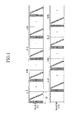
- FIG. 1 shows a driving method of a display device according to an embodiment of the present invention.
- FIG. 2 shows a display device according to an embodiment of the present invention.
- FIG. 3 shows a plurality of frames displayed by the display device during two frames of an image source signal.
- FIG. 4 shows a display portion according to an embodiment of the present invention.
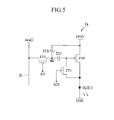
- FIG. 5 shows a first group pixel
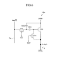
- FIG. 6 shows a second group pixel
- FIG. 7 shows a first power source voltage, a second power source voltage, a second power source voltage, a plurality of scan signals, a compensation control signal, and a data signal according to one of driving methods according to an embodiment of the present invention.
- FIG. 8 shows a first power source voltage, a second power source voltage, a plurality of scan signal, a compensation control signal, and a data signal according to another driving method of the driving methods according to an embodiment of the present invention.
- FIG. 9 shows the number of blanks between neighboring light emission periods in the driving method according to an embodiment of the present invention.
- FIG. 1 shows a driving method of a display device according to an embodiment of the present invention.
- a panel of a display device driven by the driving method according to an embodiment of the present invention includes a first group pixel E and a second group pixel O.
- the first group pixel E includes pixels emitting light in an odd-numbered frame
- the second group pixel O includes pixels emitting light in an even-numbered frame.
- sequential alignment of a plurality of odd numbered frames will be referred to as a first field EFD and sequential alignment of a plurality of even numbered frames will be referred to as a second field OFD.
- the display device displays two different first images A and B as stereoscopic images.
- the display device displays a left-eye image A_L of the image A in a frame A_LE of the first field EFD and a frame A_LO of the second field OFD and displays a right-eye image A-R of the image A in a frame A_RE of the first field EFD and a frame A_RO of the second field OFD.
- a view point of the left-eye image is a left eye and a view point of the right-eye image is a right-eye.
- the display device displays a left-eye image of the image B in a frame B_LE of the first field EFD and a frame B_LO of the second field OFD and displays a right-eye image of the image B in a frame B_RE of the first field EFD and a frame B_RO of the second field OFD.
- the present invention is not limited thereto, and the right-eye image A_R of the image A is displayed prior to the left-eye image A_L.
- the right-eye image B_R of the image B is displayed prior to the left-eye image B_L.
- Each frame sequentially includes a reset period 1, a compensation period 2, a scan period 3, and a light emission period 4. Each period will be described.
- the first field EFD and the second field OFD are driven by being synchronized while being time shifted relative to each other by a predetermined period SF.
- one frame A_LO of the second field which is temporally adjacent to one frame A_LE of the first field EFD is shifted by the period SF from one frame A_LE.
- the period SF is set to prevent the scan periods 3 of the respective fields from being overlapped with each other.
- the scan period 3 is generated, during which a data signal corresponding to each of the second group pixels is written.
- the scan period 3 is generated during which a data signal corresponding to each of the first group pixels is written.
- the light emission period 4 of the first group pixel E and the light emission period 4 of the second group pixel O are separated from each other, a maximum current for light emission duration is decreased and accordingly, the cost of a power source circuit for supplying power to the display device is reduced.
- FIG. 2 shows the display device according to an embodiment of the present invention.
- a display device 10 includes a display unit 700 and further includes one or more of an image processor 100, a timing controller 200, a data driver 300, a scan driver 400, a power controller 500, a compensation control signal unit 600, and.
- the image processor 100 generates an image display signal ImS and a synchronization signal from an input signal InS.
- the synchronization signal includes a horizontal synchronization signal Hsync, a vertical synchronization signal Vsync, and a main clock signal CLK.
- the image processor 100 determines whether the signal is a left-eye image signal (indicating a left-eye image) or a right-eye image signal (indicating a right-eye image).
- the input signal InS input to the image processor 100 includes image source signals indicating two different images, that is, a first image A and a second image B.
- the image processor 100 arranges image source signals for each frame unit according to a display sequence of the first image A and the second image B in the first group pixel E and the second group pixel O.
- the image processor 100 changes the type of an image displayed during a remaining period , which isa period that remains after a period that corresponds to integer multiples of a "unit display period" in one frame unit of the image source signal.
- the "unit display period” is a period where the first image A and the second image B are respectively time-divided and thus displayed in the first group pixel E and the second group pixel O by one frame unit of the image source signal.
- the image source signal included in the image signal InS includes a first image source signal AS indicating the first image A and a second image source signal BS indicating the second image B.
- the display device 10 displays the first image A and the second image B as a stereoscopic image.
- the first image source signal AS includes a first left-eye image signal ASL and a first right-eye image signal ASR.
- the second image source signal BS includes a second left-eye image signal BSL and a second right-eye image signal BSR.
- the image processor 100 detects the first left-eye image signal ASL, the first right-eye image signal ASR, the second left-eye image signal BSL, and the second right-eye image signal BSR from the input signal InS.
- the image processor 100 arranges the first left-eye image signal ASL, the first right-eye image signal ASR, the second left-eye image signal BSL, and the second right-eye image signal BSR according to a display sequence.
- the display sequence refers to a sequence of displaying of the first image A and the second image B in the first group pixel E and the second group pixel O of FIG. 1 .
- the first left-eye image signal ASL is displayed in the first group pixel E with one frame and in the second group pixel O with one frame
- the first right-eye image signal ASR is displayed in the first group pixel E with one frame and in the second group pixel O with one frame.
- the second left-eye image signal BSL is displayed in the first group pixel E with one frame and in the second group pixel O with one frame
- the second right-eye image signal BSR is displayed in the first group pixel E with one frame and in the second group pixel O with one frame.
- the unit display period corresponds to a period during which 8 frames are displayed (i.e. ASL_E, ASL_O, ASR_E, ASR_O, BSL_E, BSL_O, BSR_E, BSR_O).
- the image processor 100 divides the first left-eye image signal ASL into an image signal ASL_E written in the first group pixel E and an image signal ASL_O written in the second group pixel O. Similarly, the image processor 100 divides the first right-eye image signal ASR, the second left-eye image signal BSL, and the second right-eye image signal BSR respectively as image signals ASR_E, BSL_E, and BSR_E written in the first group pixel E and image signals ASR_O, BSL_O, and BSR_O written in the second group pixel O.
- the image processor 100 arranges the image signals ASL_E, ASR_E, BSL_E, and BSR_E and the image signals ASL_O, ASR_O, BSL_O, and BSR_O in one frame unit according to the display sequence.
- the basic alignment is formed by arranging each frame of each of the plurality of image signals ASL_E, ASL_O, ASR_E, ASR_O, BSL_E, BSL_O, BSR_E, and BSR_O according to the display sequence of FIG. 1 .
- the basic alignment of the present invention is not limited thereto.
- the image processor 100 arranges each frame of the plurality of image signals as ASR_E, ASR_O, ASL_E, ASL_O, BSR_E, BSR_O, BSL_E, and BSL_O.
- FIG. 3 shows a plurality of frames displayed by the display device during two frames of an image source signal according to an embodiment of the current invention.
- FIG. 3 uses the reference numerals of FIG. 1 to determine a light emission period 4 of each frame of the display device 10.
- A_LE and A_LO respectively indicates a light emission period 4 of one frame A_LE of a first field EFD and a light emission period 4 of one frame A_LO of a second frame OFD.
- one frame of an image source signal corresponds to a period from a time T1 to a time T2 and a successive frame unit of the image source signal corresponds to a period from the time T2 to a time T3.
- FIG. 3 illustrates that a unit display period PB is included two times (PB_1 and PB_2) in the period T1 to T2.
- the unit display period PB is a period during which an image is displayed according to the basic alignment.
- the unit display period PB may include the above-stated sequence of image signals ASL_E, ASL_O, ASR_E, ASR_O, BSL_E, BSL_O, BSR_E, and BSR_O, or integer multiples of the sequence.
- PR is a period that remains after dividing one frame unit of the image source signal (i.e., dividing T1 to T2, or dividing T2 to T3) by an integer multiple of the unit display period PB.
- the image type signals displayed during the remaining period PR are changed with each frame unit of the image source signal.
- image type may alternate during the remaining period PR, i.e., the display of the first image A and the display of the second image B during the remaining period PR may alternate with each successive frame unit of the image source signal (e.g., A in PR_1 of T1 to T2, and B in PR_2 of T2 to T3).
- a period that is an integer multiple of the unit display period PB (e.g., 2 times PB; the integer is 2 in FIG. 3 ) is used to display an image according to the basic alignment, and the remaining period PR is used to display the first image A or the second image B as a stereoscopic image.
- two times PB plus PR for either A or B occurs in the respective image source signal frames T1 to T2 and T2 to T3.
- the type of the image (the first image A or the second image B) displayed during the remaining period PR may be changed per one frame unit of the image source signal.
- FIG. 3 uses the reference numerals of FIG. 1 to determine the light emission period 4 of each frame of the display device 10.
- A_LE and A_LO respectively indicate the light emission period 4 of the frame A_LE of the first field EFD and the light emission period 4 of the frame A_LO of the second field OFD.
- FIG. 3 illustrates that the unit display period PB is included two times in the period T1 to T2, but the present invention is not limited thereto. That is, the period T1 to T2 can include integer multiples of the unit display period PB, e.g. where the integer is an integer other than two.
- PR is the period that remains after dividing one frame unit of the image source signal (i.e., dividing T1 to T2, or dividing T2 to T3) by the an integer multiple of the unit display period PB.
- the remaining period from dividing of the period T1 to T2 with the unit display period PB is PR_1. That is, during a remaining period PR1 in the unit frame T1 to T2 in FIG. 3 , the display device 10 displays image signals ASL_E, ASL_O, ASR_E, and ASR_O of the first image A.
- the display device 10 displays image signals BSL_E, BSL_O, BSR_E, and BSR_O of the second image B.
- the image processor 100 alternately selects one of the first image A and the second image B for each frame unit of the image source signal, and additionally arranges image signals indicating the selected image after an integer multiple (two times in FIG. 3 ) of the unit display period PB.
- the image processor 100 generates an image display signal ImS by arranging the image signals ASL_E, ASL_O, ASR_E, ASR_O, BSL_E, BSL_O, BSR_E, and BSR_O indicating the first image A and the second image B for each frame unit of the image source signal.
- the image processor 100 generates a vertical synchronization signal Vsync, a horizontal synchronization signal Hsync, and a main clock signal CLK according to a driving frequency of the display device 10.
- the image processor 100 determines the number of times of basic alignment by dividing the driving frequency of the display device with a frame frequency of the image signal, and calculates a remaining period.
- the display device 10 displays 20 images during one frame unit of the image source signal.
- the basic alignment is formed of 8 frames of the display device 10, and therefore the image processor 100 determines the number of times of the basic alignment to 2 and calculates the remaining period to four frames of the display device.
- the image processor also 100 determines the type of an image alternately displayed during the remaining period for each frame unit of the image source signal.
- the image processor 100 determines the number of times of basic alignment, a remaining period, and the type of image displayed during the remaining period for each frame unit of the image source signal, and generates an image display signal ImS by arranging image signals according to the determination result.
- the timing controller 200 generates first to fourth driving control signals CONT1 to CONT4 and an image data signal ImD according to the image display signal ImS, the vertical synchronization signal Vsync, the horizontal synchronization signal Hsync, and the main clock signal CLK.
- the timing controller 200 determines the image display signal ImS by a frame unit of the first or second field according to the vertical synchronization signal Vsync, generates the image data signal ImD by determining the image display signal ImS with a scan line unit according to the horizontal synchronization signal Hsync, and transmits the image data signal ImD and the first driving control signal CONT1 to the data driver 300.
- the data driver 300 samples and holds the image data signal ImD input according to the first driving control signal CONT1, and transmits a plurality of data signals data[1] to data[m] to respective data lines.
- the scan driver 400 generates a plurality of scan signals S[1] to S[n] with a gate-on level during a reset period 1 and a compensation period 2, simultaneously transmits a plurality of scan lines, sequentially generates the plurality of scan signals S[1] to S[n] with the gate-on level, and transmits the scan signal to the corresponding scan line among the plurality of scan lines according to the second driving control signal CONT2.
- the scan driver 400 generates all the plurality of scan signals S[1] to S[n] with a gate-off level.
- the power controller 500 determines levels of power source voltages EVDD, EVSS, OVDD, and OVSS according to a reset period 1, a compensation period 2, a scan period 3, and a light emission period 4 of each of the first group pixel and the second group pixel according to the third driving control signal, and supplies the power source voltages to a power source line.
- the compensation control signal unit 600 determines levels of compensation control signals CGE and GCO during a compensation period 2 of each of the first and second group pixels according to the fourth driving control signal CONT4 and supplies the compensation control signals to a control signal line.
- the timing controller 200 generates a first spectacles driving signal GDS1 for controlling opening and closing of a left-eye lens 800_L and a right-eye lens 800_R of first shutter spectacles 800 and a second spectacles driving signal GDS2 for controlling of operation of a left-eye lens 900_L and a right-eye lens 900_R of second shutter spectacles 900.
- the left-eye lens 800_L of the first shutter spectacles 800 is opened and the right-eye lens 800_R of the first shutter spectacles 800 is closed by the first spectacles driving signal GDS1 for a period PS1 during which an image according to left-eye image signals ASL_E and ASL_O of the first image A is displayed.
- the left-eye lens 800_L of the first shutter spectacles 800 is closed and the right-eye lens 800_R thereof is opened by the first spectacles driving signal GDS1.
- the left-eye lens 900_L of the second shutter spectacles 900 is opened and the right-eye lens 900_R thereof is closed by the second spectacles driving signal GDS2.
- the right-eye lens 900_R of the second shutter spectacles 900 is opened and the left-eye lens 900_L thereof is closed by the second spectacles driving signal GDS2.
- the display unit 700 includes a plurality of pixels as a display area including the first group pixels E and the second group pixels O.
- a plurality of data lines transmitting the plurality of data signals data[1]-data[n], a plurality of scan lines transmitting a plurality of scan signals S[1]-S[n], a plurality of power source lines, and a plurality of control signal lines are formed in the plurality of pixels, and the plurality of pixels are formed in areas where the plurality of data lines and the plurality of scan lines cross each other.
- FIG. 4 shows the display unit according to an embodiment of the present invention.
- the first group pixels E and the second group pixels O are arranged in a 2x1 pattern, but the present invention is not limited thereto.
- FIG. 4 illustrates a plurality of scan lines S1 to Sn transmitting a plurality of scan signals S[1]-S[n], a plurality of data lines D1 to Dm transmitting a plurality of data signals data[1]-data[m], a plurality of power source wires (VDDE1-VDDEk+1) supplying the power source voltage EVDD to the first group pixels E, a plurality of second power source wires (VDDO1-VDDOk) supplying the power source voltage OVDD to the second group pixels O, a plurality of first control signal lines (GCE1-GCEr) transmitting the compensation control signal GCE to the first group pixels E, and a plurality of second control signal lines (GCO1-GCOr+1) transmitting the compensation signal GCO to the second group pixels O.
- VDDE1-VDDEk+1 power source wires
- VDDO1-VDDOk supplying the power source voltage OVDD to the second group pixels O
- GCE1-GCEr
- the plurality of first control signal lines (GCE1-GCEr) and the plurality of second control signal lines (GCO1-GCOr+1) are alternately arranged row by row.
- the plurality of first power source wires (VDDE1-VDDEk+1) and the plurality of second power source wires (VDDO1-VDDOk) are alternately arranged column by column.
- the present invention is not limited thereto, and the plurality of first control signal lines (GCE1-GCEr) and the plurality of second control signal lines (GCO1-GCOr+1) are alternately arranged column by column and the plurality of first power source wires (VDDE1-VDDEk+1) and the plurality of second power source wires (VDDO1-VDDOk) are alternately arranged row by row.
- a plurality of first control signal lines (GCE1-GCEr) and the plurality of second control signal lines (GCO1-GCOr+1) are arranged row by row, and other plurality of first control signal lines and other plurality of second control signal lines are alternately arranged column by column.
- areas where a plurality of first control signal lines arranged in a row direction and a plurality of first control signal lines arranged in a column direction cross each other form a node where an electric connection is established.
- areas where the plurality of second control signal lines arranged in a row direction and the plurality of second control signal lines arranged in a column direction cross each other form a node where an electric connection is established.
- This is called a mesh structure.
- the plurality of first power source wires and the plurality of second power source wires is formed in the mesh structure.
- the first group pixel E and the second group pixel O are alternately arranged in a 2x1 pattern in areas where the plurality of scan lines S1-Sm and the plurality of data lines D1-Dm cross each other.
- the alignment pattern of the first and second group pixels E and O is not limited to the 2x1 pattern, and various patterns can be applied.
- each row the first group pixels E and the second group pixels O are alternately arranged.
- Each of the plurality of scan lines S1-Sn is connected with the first group pixel E and the second group pixel O of each row.
- Each of the plurality of data lines D1-Dm is connected to the first group pixel E and the second group pixel O of each column.
- the second group pixels O connected to the scan lines S1 and Sn are connected to the second compensation control lines (GCO1 and GCOr+1).
- the first group pixel E connected to the scan line S1 and the first group pixel E connected to the second scan line S2 are connected to the first compensation control line GCE1.
- the second group pixel O connected to the scan line S2 and the second group pixel O connected to the scan line S3 are connected to the second compensation control line GCO2.
- the first group pixels E and the second group pixels O are connected to the corresponding first or second compensation control line.
- the first group pixels E connected to the data lines D1 and Dm are connected to the first power source wires (VDDE1 and VDDEk+1).
- the first group pixels E connected to the data lines D2 and D3 are connected to the first power source wire VDDE2.
- the second group pixels O connected to the data lines D1 and D2 are connected to the first power source wire VDDO1.
- the first group pixels E and the second group pixels O are connected to the corresponding first or second compensation control line.
- FIG. 5 shows the first group pixel.
- FIG. 5 illustrates a first group pixel Eij connected to the scan line Si and the data line Dj.
- one pixel Eij of the first group pixels E includes a switching transistor ETS, a driving transistor ETR, a compensation transistor ETH, a compensation capacitor ECH, and a storage capacitor ECS.
- the driving transistor ETR includes a drain electrode connected with an anode of an organic light emitting diode OLED_E, a gate electrode connected to a first electrode of the compensation capacitor ECH, and a source electrode connected to the first power source voltage EVDD.
- the driving transistor ETR controls a driving current supplied to the organic light emitting diode OLED_E.
- the compensation transistor ETH includes a gate electrode to which a first compensation control signal GCE is input and two electrodes respectively connected to the drain electrode and the gate electrode of the driving transistor ETR.
- a second electrode of the compensation capacitor ETH is connected to a first electrode of the storage capacitor ECS and a first electrode of the switching transistor ETS.
- a second electrode of the storage capacitor ECS is connected to the first power source voltage EVDD.
- a scan signal S[i] is input to the gate electrode of the switching transistor ETS and the second electrode of the switching transistor ETS is connected to the data line Dj.
- the data signal data[j] is transmitted through the data line Dj.
- a cathode of the organic light emitting diode OLED_E is connected to the second power source voltage EVSS.
- the first power source voltage EVDD and the second power source voltage EVSS supply driving voltages for pixel operation.
- the first power source voltage EVDD and the second power source voltage EVSS supply driving voltages for operation of each of the driving transistor ETR and the organic light emitting diode OLED_E during the reset period 1, the compensation period 2, the scan period 3, and the light emission period 4.
- a power source voltage connected to an anode through the driving transistor is referred to as a first power source voltage without regard to the first group pixels E and the second group pixels O
- a power source voltage connected to a cathode is referred to as a second power source voltage without regard to the first group pixels E and the second group pixels O.
- FIG. 6 shows the second group pixel O.
- FIG. 6 illustrates a second group pixel Opq connected to a scan line Sp and a data line Dq.
- one pixel Opq of the second group pixels O includes a switching transistor OTS, a driving transistor OTR, a compensation transistor OTH, a compensation capacitor OCH, and a storage capacitor OCS.
- the driving transistor OTR includes a drain electrode connected to the anode of an organic light emitting diode OLED_O, a gate electrode connected to a first electrode of the compensation capacitor OCH, and a source electrode connected to a third power source voltage OVDD.
- the compensation transistor OTH includes a gate electrode to which a second compensation control signal GCO is input and two electrodes respectively connected to the drain electrode and the gate electrode of the driving transistor OTR.
- the second electrode of the compensation capacitor OCH is connected to a first electrode of the storage capacitor OCS and a first electrode of the switching transistor OTS.
- a second electrode of the storage capacitor OCS is connected to the first power source voltage EVDD.
- a scan signal S[p] is input to the gate electrode of the switching transistor OTS, and the second electrode of the switching transistor OTS is connected with a data line Dq.
- a data signal [q] is transmitted through the data line Dq.
- the cathode of the organic light emitting diode OLED_O is connected to the second power source voltage OVSS.
- the first power source voltage OVDD has at least two levels according to the reset period 1, the compensation period 2, the scan period 3, and the light emission period 4.
- the second compensation control signal GCO has a level that turns on the compensation transistor OTH only during the compensation period 2.
- FIG. 7 shows a first power source voltage, a second power source voltage, a plurality of scan signals, a compensation control signal, and a data signal according to one of the driving methods of an embodiment of the present invention.
- FIG. 7 illustrates that an initialization period is further included before a reset period 1, but an embodiment of the present invention does not include the initial period.
- FIG. 7 shows waveforms of signals during one frame period of a first field. However, waveforms of signals during one frame period of a second field are the same as the waveforms shown in FIG. 7 . Pixel operation by each signal will also be described with reference to FIG. 5 .
- scan signals S[1]-S[n] are changed from high level to low level.
- the driving transistor ETR is turned off.
- all the pixels are reset to a predetermined voltage. Since the initialization period is provided before operation of each frame begins, any influence of the previous frame can be eliminated and all the pixels perform compensation operation and data signal input operation under the same condition.
- an input data signal input to the previous frame can be prevented from changing the initial operation state of the driving transistor. That is, deterioration of display quality such as after-image, moving picture echo, crosstalk between left-eye and right-eye view points in 3D display can be prevented and display quality can be made uniform.
- the second power source voltage EVSS is maintained in high level during a reset period 1, and the plurality of data signals data[1]-data[n] become low level during the reset period 1 and maintain the low level for a predetermined period RT1.
- the gate voltage of the driving transistors ETR and OTR of the pixel can be sufficiently decreased such that the driving transistors ETR and OTR can provide much more current.
- a voltage stored in an intrinsic capacitor of the organic light emitting diode OLED is discharged to make the anode voltages of the organic light emitting diodes OLED_E and OLED_O equal the power source voltages EVDD and OVDD during the reset period 1.
- the voltage stored in the intrinsic capacitor is higher by about 0 to 3V than VSS.
- the voltage of the data signals data[1]-data[n] becomes the lowest value such that the current driving capability of the driving transistors ETR and OTR becomes maximized, and accordingly the anode voltage of the organic light emitting diode OLED can be decreased within the shortest time.
- the level of the plurality of scan signals S[1]-S[n] should be low level during at least a period overlapped with the period RT1 for a predetermined time period.
- the plurality of scan signals S[1]-S[n] are set to be in low level during the reset period 1 and the compensation period 2.
- FIG. 7 illustrates the scan signal S[i] among the plurality of scan signals S[1]-S[n].
- a predetermined interval PT1 is provided between the reset period 1 and the compensation period 2.
- the second power source voltage EVSS is decreased to low level (i.e., 0V) at the termination time point of the reset period 1.
- the first compensation control signal GCE is decreased to low level at the start time point of the compensation period 2, and the first compensation control signal GCE maintains the low level during the compensation period 2.
- the plurality of data signals data[1]-data[m] are high level, and the first power source voltage EVDD maintains the low level.
- the compensation transistor ETH is turned on according to the first compensation control signal GCE and thus the driving transistor ETR is diode-connected, and a voltage acquired by subtracting a threshold voltage VTH of the driving transistor ETR from the first power source voltage EVDD is supplied to the gate electrode of the driving transistor ETR.
- the compensation capacitor ECH is charged with a voltage corresponds to a difference between the voltage of the data signal data[j] and the (EVDD-VTH) voltage.
- a predetermined interval PT2 is provided between the compensation period 2 and the scan period 3, and the plurality of scan signals S[1]-S[i] become high level during the interval PT2.
- the plurality of scan signals S[1]-S[n] sequentially become low level such that the switching transistor ETS is turned on. While the switching transistor ETS is in the turn-on state, the data signal data[j] is transmitted to a node ND where the second electrode of the compensation capacitor ECH and the first electrode of the storage capacitor ECS meet each other.
- the first electrode of the compensation capacitor ECH is connected to the gate electrode of the driving transistor ETR and is being floated.
- the variation of a voltage of the node ND is distributed according to a capacitor ratio between the storage capacitor ECS and the compensation capacitor ECH, and the voltage variation ⁇ V distributed to the compensation capacitor ECH is reflected to the gate voltage of the driving transistor ETR.
- the gate voltage of the driving transistor ETR becomes EVDD-VTH+ ⁇ V.
- EVDD is an EVDD voltage level during the compensation period, that is, 3V for example.
- the plurality of data signals data[1]-data[m] become high level voltages, and a predetermined interval PT3 is provided between the scan period 3 and the light emission period 4.
- the first power source voltage EVDD is increased to high level and the plurality of scan signals S[1]-S[n] are increased from the high level to a further higher level.
- the scan signal S[i] is increased to the further higher level, the switching transistor ETS performs full-off such that a leakage current that occurs during the light emission period 4 can be blocked. Since the voltage of the node ND is approximately included within a voltage range of the data line Dj before the light emission period 4, a voltage difference between the drain electrode and the source electrode of the switch transistor ETS is insignificant.
- the voltage of the node ND and the gate voltage of the driving transistor ETR are increased due to coupling of the capacitors ECS and ECH.
- the voltage of the node ND is also increased by 10V so that the drain-source voltage of the switching transistor ETS is correspondingly increased.
- the leakage current of the transistor is proportional to the drain-source voltage, the amount of the leakage current flowing to the data line from the node ND is increased.
- the drain-source voltage can be decreased and accordingly the leakage current can be reduced.
- the voltage of the node ND is included in the voltage range right after the scan period.
- the voltage of the node ND has the voltage range of 11 V to 16V, and in the worst case, the voltage of the data line Dj becomes 1V and the voltage of the node ND becomes 16V so that the drain-source voltage of the switching transistor becomes 15V.
- the leakage current can be reduced approximately to 1/6 (15/2.5).
- a driving current is generated in the driving transistor ETR due to a source-gate voltage difference. Since a voltage obtained by subtracting the gate voltage EVDD(3V)-Vth+ ⁇ V from the source voltage EVDD 12V of the driving transistor ETR and then the threshold voltage VTH is subtracted from the voltage, a driving current of the driving transistor ETR becomes a current corresponding to a square of the voltage (9V- ⁇ V). That is, deviation due to the same data signals between driving currents does not occur due to a threshold voltage deviation between the driving transistors.
- the first power source voltage EVDD becomes low level and a light emission off period PT4 is generated.
- the light emission off period PT4 is provided between the next frame and a current frame and pixels do not emit light during the light emission off period PT4.
- FIG. 7 illustrates pixels emitting light in the first field EFD, but pixels emitting light in the second field OFD emit light through the same method of the pixels emitting in the first field EFD.
- a high level or a low level is an example of a voltage level, and the voltage level is not limited thereto.
- FIG. 8 shows a first power source voltage, a second power source voltage, a plurality of scan signals, a compensation control signal, and a data signal.
- second power source voltages EVSS and OVSS are maintained with a constant voltage and supplied to one electrode of each pixel without regarding the first group pixels and the second group pixels.
- the light emission period 4 of the first field EFD and the reset period 1 of the second field OFD should not overlap each other, and the light emission period 4 of the second field OFD and the reset period 1 of the first field EFD should not overlap each other.
- a first power source voltage EVDD is lower than the first power source voltage EVDD in the reset period 1 of FIG. 1 .
- the first power source voltage EVDD of FIG. 7 is 0V and the first power source voltage EVDD of FIG. 8 is -3V.
- the second power source voltage EVSS is maintained in low level, that is, 0V.
- the anode voltage of the organic light emitting diode OLED becomes higher than the first power source voltage EVDD, and the anode of the organic light emitting diode becomes a source of the driving transistor.
- Gate voltages of the driving transistors ETR and OTR are approximately similar to the first and second power source voltages EVDD and OVDD, and the anode voltages of the organic light emitting diodes OLED_E and OLED_O are voltages (power source voltage VSS + voltages (0 to 3V) stored in the organic light emitting diodes OLED_E and OLED_O) and therefore a gate-source voltage of each of the driving transistors ETR and OTR becomes a sufficient negative voltage such that the driving transistors ETR and OTR are turned on.
- a current flowing through the driving transistors ETR and OTR flows toward the first and second power source voltages EVDD and OVDD from the anodes of the organic light emitting diodes OLED_E and OLED_O, and eventually it flows until the anode voltages of the organic light emitting diodes OLED_E and OLED_O become equal to the power source voltages EVDD and OVDD.
- the gate voltages of the driving transistors ETR and OTR may not be able to be sufficiently low.
- voltages of the data signals data[1]-data[m] are set to be low voltages and the scan signals S[1]-S[n] are set at a low level to lower the gate voltages during the reset period 1.
- the data signal becomes a low voltage during the reset period 1.
- the present invention is not limited thereto, and when the power source voltage EVDD is sufficiently low, the data signal does not need to be changed to a low level and all the scan signals can be set to a high level.
- the first power source voltage EVDD is increased to 3V from -3V. Operation of remaining periods are the same as that described with reference to FIG. 7 , and therefore no further description will be provided.
- the display device alternately displays one of the image A and the image B by each frame unit of an image signal during remaining periods in one frame unit of the image source signal. Accordingly, a difference in image quality between the two images can be prevented.
- a predetermined blank period is provided between the plurality of light emission periods A_LE, A_LO, A_RE, A_RO, B_LE, B_LO, B_RE, and B_RO shown in FIG. 3 .
- the blank period corresponds to a period between the light emission period 4 of the first field EFD and a light emission period 4 of its neighboring second field OED of FIG. 1 .
- the blank period is represented by the number of blanks.
- the blank period is extended as the number of blanks is increased.
- the number of blanks in one frame of an image source signal is set to 90.
- the present invention is not limited thereto.
- the number of blanks for each light emission period becomes 4.5 if the 90 blanks are evenly divided.
- 0.5 is a fractional number (i.e. having a non-zero didgut) below the decimal point, and requires much more memory capacity when being realized as a digital signal.
- accurate and even division of the blanks for each light emission period requires complicated logic and causes costs to increase.
- blank periods between fields are set to be different from each other according to the type of an image between adjacent fields.
- blank periods between fields are set to be different from each other according to a view point of an image between adjacent fields.
- the left-eye image is an image generated with a view point of left-eye and the right-eye image is an image generated with a view point of right-eye.
- the number of blanks between fields set to be different from each other is determined according to the type of an image and a view point of an image between adjacent fields.
- the numbers of blanks between fields are set to be different from each other according to at least one of the type of an image and a view point of an image between adjacent fields.
- the number of blanks is set to be an integer that does not have numbers below the decimal point (i.e. a whole or non-fractional number).
- FIG. 9 shows the numbers of blanks between respective adjacent light emission periods in the driving method according to an embodiment of the present invention.
- a default number of blanks between a first field and a second field is acquired by dividing the number of blanks allocated to each frame of an image source signal by the number of frames of the display device 10, included in one frame unit of the image source signal and eliminating numbers below the decimal point from the division result.
- the number of blanks between a left-eye image and a right-eye image is larger by 1 than the default number of blanks. Further, the number of blanks between fields of different images is greater by 1 than the default number of blanks. "1" is an example, and remaining blanks are distributed to prevent a total number of blanks during one frame of an image source signal from having numbers below the decimal point.
- the number of blanks between the first field in which the left-eye image A_LE of the first image A is displayed and the second field in which the left-eye image A_LO of the first image A is displayed is set to 4.
- the number of blanks between the second field in which the left-eye image A_LO of the first image A is displayed and the first field in which the right-eye image A_RE of the first image A is displayed is set to 5.
- the number of blanks between the second field in which the right-eye image A_RO of the first image A is displayed and the first field in which the left-eye image B_LE of the second image B is set to 5.
- a blank period can be controlled through such a method, thereby reducing and/or preventing occurrence of flickering.
- the timing controller 200 sets the numbers of blanks between horizontal synchronization signals Vsync to be different from each other according to the type of an image or a view point of an image between adjacent fields to realize the method of FIG. 9 .
- the number of blanks between the vertical synchronization signals Vsync implies the number of blanks between a time point instructing termination of the previous frame and a time point instructing start of a current frame.
- the timing controller 200 sets a default number of blanks 4 between vertical synchronization signals Vsync of each of adjacent fields displaying the same image, the number of blanks 5 between vertical synchronization signals Vsync of each of adjacent fields respectively displaying different images, and the number of blanks 5 between vertical synchronization signals Vsync of each of adjacent fields respectively having a different image view point to be different from each other.
- the number of blanks 5 between the vertical synchronization signals Vsync of each of the adjacent fields respectively displaying different images and the number of blanks 5 between the vertical synchronization signals Vsync of each of the adjacent fields respectively having the different image view point are set to be equal to each other, but the present invention is not limited thereto. That is, the two numbers of blanks are set to be different from each other.
- an image quality difference between a first image A and a second image B results when one of the first image A and the second image B is displayed one more time than the other image when, e.g., 10 images are formed in one frame period.
- embodiments provide a display device that can reduce motion artifacts and increase light emission duration, and a driving method thereof.
- Embodiments of the invention provide a display device that can display a stereoscopic image with a lower driving frequency in a large and/or high-resolution display device, and a driving method thereof.
- a display device that can prevent image quality difference between two different images displayed therein, and a driving method thereof is be provided.
- embodiments of the invention provide a display device that can display a stereoscopic image or a planar image in large and/or high resolution of the display device.
- Embodiments can be applied to, e.g., an active matrix type display device and a driving method thereof.
Landscapes
- Engineering & Computer Science (AREA)
- Multimedia (AREA)
- Signal Processing (AREA)
- Physics & Mathematics (AREA)
- Computer Hardware Design (AREA)
- General Physics & Mathematics (AREA)
- Theoretical Computer Science (AREA)
- Control Of Indicators Other Than Cathode Ray Tubes (AREA)
- Control Of El Displays (AREA)
- Electroluminescent Light Sources (AREA)
Abstract
Description
- An embodiment of the present invention relates to a display device and a driving method thereof. In Particular, embodiments of the present invention relate to an active matrix type display device and a driving method thereof.
- When a display device displays a stereoscopic (i.e. 3D) image, the display device alternately displays a left-eye image and a right-eye image. In this case, a frame frequency of an image source signal input to the display device is different from a driving frequency of the display device.
- For example, when a driving frequency of the display device is 240Hz and a frame frequency of the image source signal is 24Hz, a total of 10 left-eye and right-eye images are displayed in the display device during one frame period of the image source signal.
- When the display device displays two different images A and B as a stereoscopic image under such a condition, the display device arranges a left-eye image and a right-eye image of the first image A and a left-eye image and a right-eye image of the second image B to form 10 images during one frame period of the image source signal. However, when 10 images are formed in one frame period, one of the first image A and the second image B is displayed one more time than the other image.
- This causes an image quality difference between the first image A and the second image B.
- The above information disclosed in this Background section is only for enhancement of understanding of the background of the invention and therefore it may contain information that does not form prior art that is already known to a person of ordinary skill in the art.
- The present invention has been made in an effort to provide a display device that can display a stereoscopic image or a planar image in an environment requiring at least one of enlargement of the display device and high resolution of the display device.
- A display device according to an embodiment of the present invention configured to display a selected image type, the image type comprising a first image and a second image according to an image source signal. The display device includes: a display unit including a first group pixel and a second group pixel and an image processor adapted to arrange the image source signals for each frame of the display device according to a sequence of displaying the first image and the second image in a first group pixel and a second group pixel.
- The image processor changes the image type displayed during remaining period, where the remaining period is a period remaining after dividing the frame unit of the image source signal by an integer multiple of a unit display period. The unit display period is a period during which the first image and the second image are displayed in the first group pixel and the second group pixel for each frame. The image processor adds an image source signal alignment corresponding to the remaining period to an image source signal alignment of a period corresponding to the integer multiple of the unit display period
- The image processor is adapted to determine a first left-eye image signal, a first right-eye image signal, a second left-eye image signal, and a second right-eye image signal included in the image source signalas an image signal respectively displayed in the first group pixel and the second group pixel per one frame unit of the image source signal, and forms a basic alignment corresponding to the unit display period by arranging the determined image signals according to the display sequence.
- The image processor is adapted to form the basic alignment by arranging image signals according to a sequence of an image signal displayed in the first group pixel among the first left-eye image signal, an image signal displayed in the second group pixel among the first left-eye image signal, an image signal displayed in the first group pixel among the first right-eye image signal, an image signal displayed in the second group pixel among the first right-eye image signal, an image signal displayed in the first group pixel among the second left-eye image signal, an image signal displayed in the second group pixel among the second left-eye image signal, an image signal displayed in the first group pixel among the second right-eye image signal, and an image signal displayed in the second group pixel among the second right-eye image signal.
- The image processor is adapted to form the basic alignment by arranging image signals according to a sequence of an image signal displayed in the first group pixel among the first right-eye image signal, an image signal displayed in the second group pixel among the first right-eye image signal, an image signal displayed in the first group pixel among the first left-eye image signal, an image signal displayed in the second group pixel among the first left-eye image signal, an image signal displayed in the first group pixel among the second right-eye image signal, an image signal displayed in the second group pixel among the second right-eye image signal, an image signal displayed in the first group pixel among the second left-eye image signal, and an image signal displayed in the second group pixel among the second left-eye image signal.
- The image processor is adapted to repeat the basic alignment integer times the unit display period, and arranges image signals of the type of an image corresponding to the current frame of the image source signal among the determined image signals number of times of the number of frames of the display device and adds the alignment to the repeated basic alignment.
- In embodiments of the invention, the display unit further includes a plurality of scan lines transmitting a plurality of scan signals to the first and second group pixels, a plurality of data lines transmitting a plurality of data lines to the first and second group pixels and a light emission period during which the first group pixels emit light according to the plurality of data signals and a scan period during which the plurality of data signals transmitted to the second group pixels overlap each other. Optionally, the plurality of data signals depend on the image source signals arranged by the image processor.
- Each of the first and second group pixels includes a driving transistor providing a driving current according to a written data signal and an organic light emitting diode connected to the driving transistor and emitting light according to the driving current, wherein a first power source voltage applied to the driving transistor is lower than a second power source voltage applied to a cathode of the organic light emitting diode during a reset period, said reset period being a period during which a voltage of an anode of the organic light emitting diode is reset.
- In embodiments of the invention, each of the first and second group pixels further includes a capacitor connected to a gate of the driving transistor, the capacitor being coupled to the first power source voltage, wherein a threshold voltage of the driving transistor is stored in the capacitor during a compensation period, the compensation period being a period during which the driving transistor is diode-connected.
- In embodiments of the invention, during the light emission period, the first power source voltage is higher than the first power source voltage of the reset period, the compensation period, and the scan period.
- In yet further embodiments of the invention, one frame of the display device includes the reset period, the compensation period, the scan period, and the light emission period, and is operated in a sequence of the reset period, the compensation period, the scan period, and the light emission period.
- In still further embodiments of the invention, blank periods between first fields formed of frames in which the first group pixel emits light and second fields formed of frames in which the second group pixel emits light are set to be different from each other according to at least one of the image type and a view point of an image between the adjacent first and second fields.
- The numbers of blanks between the first fields and the second fields are set to be different from each other according to at least one of the image type and the view point of the image, the number of blanks between the first field and the second field indicating a period between a light emission period of the first field and a light emission period of the second field that is adjacent to the first field.
- In yet still further embodiments, the numbers of blanks are set to be different from each other according to at least one of the type of the image and the view point of the image in order to prevent the number of blanks from being a fractional number.
- A default number of blanks is set to an integer acquired by dividing the number of blanks allocated to each frame unit of the image source signal by the number of frames of the display device included in one frame unit of the image source signal and eliminating fractional numbers from the division result, and when the image type of the first field is different from the image type of the adjacent second field , the number of blanks is set to be greater than the default number of blanks.
- In further embodiments, the display device sets the number of blanks to be greater than the default number of blanks when a view point of an image of the first field is different from that a view point of an image of the adjacent second field.
- In further embodiments, the display device further includes a timing controller setting the numbers of blanks between the vertical synchronization signals to be different from each other according to the type of an image and a view point of an image between adjacent fields.
- In yet further embodiments, the display device is adapted to operate in concert with first shutter spectacles that are opened while the first image is displayed in the first group pixel and the second group pixel and second shutter spectacles that are opened while the second image is displayed in the first group pixel and the second group pixel.
- The first shutter spectacles includes a first left-eye lens opened while a first left-eye image signal of the first image is displayed in the first group pixel, the second group pixel and a second right-eye lens opened while a first right-eye image signal of the first image is displayed in the first group pixel and the second group pixel, and the second shutter spectacles includes a second left-eye lens opened while a second left-eye image signal of the second image is displayed in the first group pixel and the second group pixel and a second right-eye lens opened while a second right-eye image signal of the second image is displayed in the first group pixel and the second group pixel.
- A display device according to another embodiment of the present invention configured to display a selected image type, comprising a first image and a second image as a stereoscopic image according to an image source signal representing the first image and the second image. The display device includes: a display unit including a first group pixel and a second group pixel; an image processor adapted to arrange the image source signal for each frame unit of the image source signal according to a display sequence of the first image and the second image in the first group pixel and the second group pixel; and a timing controller setting blank periods between first fields formed of frames during which the first group pixel emits light and second fields formed of frames during which the second group pixel emits light according to at least one of theimage type and a view point of an image between a first field and a second field that are adjacent to each other.
- The image processor changes the type of each of images displayed during remaining periods other than a period integer multiples of a unit display period of one frame of the image source signal, and adds an image source signal alignment corresponding to the remaining periods to an image source signal alignment corresponding to the period integer times the unit display period. The image source signal includes a first left-eye image signal, a first right-eye image signal, a second left-eye image signal, and a second right-eye image signal, and the unit display period is a period during which the first left-eye image signal, the first right-eye image signal, the second left-eye image signal, and the second right-eye image signal are displayed according to the display sequence in the first group pixel and the second group pixel by one frame unit of the image source signal.
- A view point of the image of the first left-eye image signal is different from a view point of the image of the right-eye image signal, and a view point of the image of the second left-eye image signal is different from a view point of the image of the second right-eye image signal, and the unit display period is a period during which the first left-eye image signal, the first right-eye image signal, the second left-eye image signal, and the second right-eye image signal are displayed in the first group pixel and the second group pixel for each frame.
- One frame of the display device includes a scan period during which a data signal is written in a plurality of pixels and a light emission period during which the plurality of pixels emit light according to the written data signal, and a light emission period of the first field and a scan period of the second field overlap each other.
- The frame of the display device further includes a reset period for resetting an anode voltage of an organic light emitting diode of the pixel and a compensation period compensating a threshold voltage of a driving transistor supplying a driving current to the organic light emitting diode.
- A level of a first power source voltage supplied to the driving transistor is different from at least one of the reset period, the compensation period, and the scan period during the light emission period.
- A driving method of a display according to another embodiment of the present invention is applied to a display device including a first group pixel and a second group pixel. The driving method includes: arranging image source signals representing a first image and a second image according to a display sequence of the first image and the second image in the first group pixel and the second group pixel for each frame unit of the image source signal; repeating a basic alignment corresponding to a unit display period by a number of time that the unit display period is included in the frame unit of the image source signal, the unit display period being a period during which the first image and the second image are displayed in the first group pixel and the second group pixel for each frame of the display device; alternately selecting the image type to be displayed during a remaining period, the remaining period being a period after the unit display period is passed the integer multiple during one frame period of the image source signal by one frame unit of the image source signal; and adding an image source signal alignment corresponding to the remaining period to the repeated basic alignment.
- The arranging of the image source signal includes: determining each of a first left-eye image signal, a first right-eye image signal, a second left-eye image signal, and a second right-eye image signal included in the image source signal for an image signal displayed in the first group pixel and an image signal displayed in the second group pixel for each frame unit of the image source signal; and forming the basic alignment by arranging the determined image signals according to the display sequence.
- The adding of the image source signal alignment corresponding to the remaining period includes arranging image signals of the selected image type among the determined image signals by the number of frames of the display device, corresponding to the remaining period and adding the arranged image signals to the repeated basic alignment.
- In further embodiments, the driving method further includes a light emission step of the first group pixel according to a plurality of written data signals and a scan step for transmitting a plurality of data signals to the second group pixel, and the light emission step and the scan step are temporally overlapped with each other.
- In yet further embodiments, the driving method of the display device further includes: resetting a voltage of an anode of an organic light emitting diode connected to a driving transistor to which a driving current flows according to a written data signal and emitting light according to the driving current by decreasing a first power source voltage applied to the driving transistor; and a compensation step for diode-connection of the driving transistor and storing a threshold voltage of the driving transistor in a capacitor.
- In still further embodiments, the driving method of the display device further includes setting blank periods between first fields formed of frames during which the first group pixel emits light and second fields formed of frames during which the second group pixel emits light to be different from each other according to at least one of the type of an image and a view point of an image between adjacent first and second fields.
- The setting of the blank periods includes setting the numbers of blanks between the first fields and the second fields to be different from each other according to at least one of the type of an image and a view point of an image between the first field and the second field, and the number of blanks between the first field and the second field represents a period between a light emission period of the first field and a light emission period of the second field that is adjacent to the first field.
- The setting of the number of blanks includes: setting a default number of blanks with an integer acquired by dividing the number of blanks allocated to each frame of the image source signal by the number of frames of the display device, included in one frame of the image source signal and eliminating numbers below the decimal point from the division; and setting the number of blanks to be greater than the default number of blanks when the image type of the first field is different from the image type of the second field that is adjacent to the first field.
- The setting of the number of blanks includes: setting a default number of blanks with an integer acquired by dividing the number of blanks allocated to each frame of the image source signal by the number of frames of the display device, included in one frame of the image source signal and eliminating numbers below the decimal point; and setting the number of blanks to be greater than the default number of blanks when a view point of the first field is different from a view point of the second field that is adjacent to the first field.
- The present invention provides a display device that can reduce motion artifact and assure maximum light emission duration, and a driving method thereof. By such an effect, a display device that can display a stereoscopic image with a lower driving frequency than a conventional display device in an environment requiring at least one of enlargement and high-resolution of the display device, and a driving method thereof can be provided.
- In addition, a display device that can prevent image quality difference between two different images displayed therein, and a driving method thereof can be provided.
- According to an aspect of the present invention, there is provided a display device according to
Claim 1. Preferred features of this aspect are set out inClaims 2 to 10. According to a further aspect of the present invention, there is provided a driving method of a display device according to Claim 11 Preferred features of this aspect are set out in Claims 12 to 15. -
FIG. 1 shows a driving method of a display device according to an embodiment of the present invention. -
FIG. 2 shows a display device according to an embodiment of the present invention. -
FIG. 3 shows a plurality of frames displayed by the display device during two frames of an image source signal. -
FIG. 4 shows a display portion according to an embodiment of the present invention. -
FIG. 5 shows a first group pixel. -
FIG. 6 shows a second group pixel. -
FIG. 7 shows a first power source voltage, a second power source voltage, a second power source voltage, a plurality of scan signals, a compensation control signal, and a data signal according to one of driving methods according to an embodiment of the present invention. -
FIG. 8 shows a first power source voltage, a second power source voltage, a plurality of scan signal, a compensation control signal, and a data signal according to another driving method of the driving methods according to an embodiment of the present invention. -
FIG. 9 shows the number of blanks between neighboring light emission periods in the driving method according to an embodiment of the present invention. - In the following detailed description, only certain embodiments of the present invention have been shown and described, simply by way of illustration. As those skilled in the art will realize, the described embodiments can be modified in various different ways, all without departing from the scope of the presently claimed invention. Accordingly, the drawings and description are to be regarded as illustrative in nature and not restrictive. Like reference numerals designate like elements throughout the specification.
- Throughout this specification and the claims that follow, when it is described that an element is "coupled" to another element, the element can be "directly coupled" to the other element or "electrically coupled" to the other element through a third element. In addition, unless explicitly described to the contrary, the word "comprise" and variations such as "comprises" or "comprising" will be understood to imply the inclusion of stated elements but not the exclusion of any other elements.
-
FIG. 1 shows a driving method of a display device according to an embodiment of the present invention. - A panel of a display device driven by the driving method according to an embodiment of the present invention includes a first group pixel E and a second group pixel O. The first group pixel E includes pixels emitting light in an odd-numbered frame, and the second group pixel O includes pixels emitting light in an even-numbered frame. Hereinafter, sequential alignment of a plurality of odd numbered frames will be referred to as a first field EFD and sequential alignment of a plurality of even numbered frames will be referred to as a second field OFD.
- In addition, the display device displays two different first images A and B as stereoscopic images. To display the stereoscopic images, the display device displays a left-eye image A_L of the image A in a frame A_LE of the first field EFD and a frame A_LO of the second field OFD and displays a right-eye image A-R of the image A in a frame A_RE of the first field EFD and a frame A_RO of the second field OFD. A view point of the left-eye image is a left eye and a view point of the right-eye image is a right-eye.
- Subsequent to the image A, the display device displays a left-eye image of the image B in a frame B_LE of the first field EFD and a frame B_LO of the second field OFD and displays a right-eye image of the image B in a frame B_RE of the first field EFD and a frame B_RO of the second field OFD.
- However, the present invention is not limited thereto, and the right-eye image A_R of the image A is displayed prior to the left-eye image A_L. Alternatively, the right-eye image B_R of the image B is displayed prior to the left-eye image B_L.
- Each frame sequentially includes a
reset period 1, acompensation period 2, ascan period 3, and alight emission period 4. Each period will be described. - The first field EFD and the second field OFD are driven by being synchronized while being time shifted relative to each other by a predetermined period SF. In further detail, one frame A_LO of the second field which is temporally adjacent to one frame A_LE of the first field EFD is shifted by the period SF from one frame A_LE. The period SF is set to prevent the
scan periods 3 of the respective fields from being overlapped with each other. - During the
light emission period 4 of the first group pixel, thescan period 3 is generated, during which a data signal corresponding to each of the second group pixels is written. During thelight emission period 4 of the second group pixel, thescan period 3 is generated during which a data signal corresponding to each of the first group pixels is written. Thus, thescan periods 3 can be sufficiently assured and accordingly, a temporal margin for driving of the display panel can be increased. - In addition, since a scan frequency can be decreased, bandwidths of the data driver generating and transmitting the data signal and the scan driver generating the scan signal can be decreased, thereby reducing the cost of circuit parts.
- Further, since the
light emission period 4 of the first group pixel E and thelight emission period 4 of the second group pixel O are separated from each other, a maximum current for light emission duration is decreased and accordingly, the cost of a power source circuit for supplying power to the display device is reduced. -
FIG. 2 shows the display device according to an embodiment of the present invention. - As shown in
FIG. 2 , adisplay device 10 includes adisplay unit 700 and further includes one or more of animage processor 100, atiming controller 200, adata driver 300, ascan driver 400, apower controller 500, a compensationcontrol signal unit 600, and. - The
image processor 100 generates an image display signal ImS and a synchronization signal from an input signal InS. The synchronization signal includes a horizontal synchronization signal Hsync, a vertical synchronization signal Vsync, and a main clock signal CLK. - When a signal (hereinafter, an image source signal) for two images A and B included in the image signal InS is a signal displaying a stereoscopic image, the
image processor 100 determines whether the signal is a left-eye image signal (indicating a left-eye image) or a right-eye image signal (indicating a right-eye image). - The input signal InS input to the
image processor 100 according to an embodiment of the present invention includes image source signals indicating two different images, that is, a first image A and a second image B. - The
image processor 100 arranges image source signals for each frame unit according to a display sequence of the first image A and the second image B in the first group pixel E and the second group pixel O. - The
image processor 100 changes the type of an image displayed during a remaining period , which isa period that remains after a period that corresponds to integer multiples of a "unit display period" in one frame unit of the image source signal. The "unit display period" is a period where the first image A and the second image B are respectively time-divided and thus displayed in the first group pixel E and the second group pixel O by one frame unit of the image source signal. - In further detail, the image source signal included in the image signal InS includes a first image source signal AS indicating the first image A and a second image source signal BS indicating the second image B. The
display device 10 according to an embodiment of the present invention displays the first image A and the second image B as a stereoscopic image. - In this case, the first image source signal AS includes a first left-eye image signal ASL and a first right-eye image signal ASR. The second image source signal BS includes a second left-eye image signal BSL and a second right-eye image signal BSR.
- The
image processor 100 detects the first left-eye image signal ASL, the first right-eye image signal ASR, the second left-eye image signal BSL, and the second right-eye image signal BSR from the input signal InS. Theimage processor 100 arranges the first left-eye image signal ASL, the first right-eye image signal ASR, the second left-eye image signal BSL, and the second right-eye image signal BSR according to a display sequence. - The display sequence refers to a sequence of displaying of the first image A and the second image B in the first group pixel E and the second group pixel O of
FIG. 1 . For example, in an embodiment of the present invention, the first left-eye image signal ASL is displayed in the first group pixel E with one frame and in the second group pixel O with one frame, and the first right-eye image signal ASR is displayed in the first group pixel E with one frame and in the second group pixel O with one frame. Subsequently, the second left-eye image signal BSL is displayed in the first group pixel E with one frame and in the second group pixel O with one frame, and the second right-eye image signal BSR is displayed in the first group pixel E with one frame and in the second group pixel O with one frame. In this case, the unit display period corresponds to a period during which 8 frames are displayed (i.e. ASL_E, ASL_O, ASR_E, ASR_O, BSL_E, BSL_O, BSR_E, BSR_O). - Hereinafter, the 8 frames will be described as a "basic alignment" in embodiments of the present invention.
- The
image processor 100 divides the first left-eye image signal ASL into an image signal ASL_E written in the first group pixel E and an image signal ASL_O written in the second group pixel O. Similarly, theimage processor 100 divides the first right-eye image signal ASR, the second left-eye image signal BSL, and the second right-eye image signal BSR respectively as image signals ASR_E, BSL_E, and BSR_E written in the first group pixel E and image signals ASR_O, BSL_O, and BSR_O written in the second group pixel O. - The
image processor 100 arranges the image signals ASL_E, ASR_E, BSL_E, and BSR_E and the image signals ASL_O, ASR_O, BSL_O, and BSR_O in one frame unit according to the display sequence. The basic alignment is formed by arranging each frame of each of the plurality of image signals ASL_E, ASL_O, ASR_E, ASR_O, BSL_E, BSL_O, BSR_E, and BSR_O according to the display sequence ofFIG. 1 . The basic alignment of the present invention is not limited thereto. When the right-eye image is displayed ahead of the left-eye image, theimage processor 100 arranges each frame of the plurality of image signals as ASR_E, ASR_O, ASL_E, ASL_O, BSR_E, BSR_O, BSL_E, and BSL_O. -
FIG. 3 shows a plurality of frames displayed by the display device during two frames of an image source signal according to an embodiment of the current invention. -
FIG. 3 uses the reference numerals ofFIG. 1 to determine alight emission period 4 of each frame of thedisplay device 10. For example, inFIG. 3 , A_LE and A_LO respectively indicates alight emission period 4 of one frame A_LE of a first field EFD and alight emission period 4 of one frame A_LO of a second frame OFD. - In
FIG. 3 , one frame of an image source signal corresponds to a period from a time T1 to a time T2 and a successive frame unit of the image source signal corresponds to a period from the time T2 to a time T3.FIG. 3 illustrates that a unit display period PB is included two times (PB_1 and PB_2) in the period T1 to T2. The unit display period PB is a period during which an image is displayed according to the basic alignment. Thus, the unit display period PB may include the above-stated sequence of image signals ASL_E, ASL_O, ASR_E, ASR_O, BSL_E, BSL_O, BSR_E, and BSR_O, or integer multiples of the sequence. - In
FIG. 3 , PR is a period that remains after dividing one frame unit of the image source signal (i.e., dividing T1 to T2, or dividing T2 to T3) by an integer multiple of the unit display period PB. - Referring to
FIG. 3 , a driving method for driving the display device, while changing the type of the image signal (A or B) during the remaining period PR, will now be described in further detail. - In the present example embodiment, the image type signals displayed during the remaining period PR are changed with each frame unit of the image source signal. For example, image type may alternate during the remaining period PR, i.e., the display of the first image A and the display of the second image B during the remaining period PR may alternate with each successive frame unit of the image source signal (e.g., A in PR_1 of T1 to T2, and B in PR_2 of T2 to T3).
- As described above, in the present example embodiment, a period that is an integer multiple of the unit display period PB (e.g., 2 times PB; the integer is 2 in
FIG. 3 ) is used to display an image according to the basic alignment, and the remaining period PR is used to display the first image A or the second image B as a stereoscopic image. This occurs in one frame unit of the image source signal. For example, , inFIG. 3 , two times PB plus PR for either A or B occurs in the respective image source signal frames T1 to T2 and T2 to T3. Thus, the type of the image (the first image A or the second image B) displayed during the remaining period PR may be changed per one frame unit of the image source signal. -
FIG. 3 uses the reference numerals ofFIG. 1 to determine thelight emission period 4 of each frame of thedisplay device 10. For example, inFIG. 3 , A_LE and A_LO respectively indicate thelight emission period 4 of the frame A_LE of the first field EFD and thelight emission period 4 of the frame A_LO of the second field OFD. - As described above,
FIG. 3 illustrates that the unit display period PB is included two times in the period T1 to T2, but the present invention is not limited thereto. That is, the period T1 to T2 can include integer multiples of the unit display period PB, e.g. where the integer is an integer other than two. - In the presently described embodiment, PR is the period that remains after dividing one frame unit of the image source signal (i.e., dividing T1 to T2, or dividing T2 to T3) by the an integer multiple of the unit display period PB. Thus, the remaining period from dividing of the period T1 to T2 with the unit display period PB (i.e., PB_1 and PB_2) is PR_1. That is, during a remaining period PR1 in the unit frame T1 to T2 in
FIG. 3 , thedisplay device 10 displays image signals ASL_E, ASL_O, ASR_E, and ASR_O of the first image A. - Similarly, during a remaining period PR2 in a frame period T2 to T3 of the next image source signal, the
display device 10 displays image signals BSL_E, BSL_O, BSR_E, and BSR_O of the second image B. - Thus, the
image processor 100 alternately selects one of the first image A and the second image B for each frame unit of the image source signal, and additionally arranges image signals indicating the selected image after an integer multiple (two times inFIG. 3 ) of the unit display period PB. - As described, the
image processor 100 generates an image display signal ImS by arranging the image signals ASL_E, ASL_O, ASR_E, ASR_O, BSL_E, BSL_O, BSR_E, and BSR_O indicating the first image A and the second image B for each frame unit of the image source signal. - The
image processor 100 generates a vertical synchronization signal Vsync, a horizontal synchronization signal Hsync, and a main clock signal CLK according to a driving frequency of thedisplay device 10. Theimage processor 100 determines the number of times of basic alignment by dividing the driving frequency of the display device with a frame frequency of the image signal, and calculates a remaining period. - When the frame frequency is 24Hz and the driving frequency is 240Hz, the result of the division becomes 10. As shown in
FIG. 1 , one frame of the first field EFD and one frame of the second field OFD are displayed during one period operation of thedisplay device 10. Thus, thedisplay device 10 displays 20 images during one frame unit of the image source signal. The basic alignment is formed of 8 frames of thedisplay device 10, and therefore theimage processor 100 determines the number of times of the basic alignment to 2 and calculates the remaining period to four frames of the display device. - The image processor also 100 determines the type of an image alternately displayed during the remaining period for each frame unit of the image source signal.
- As described, the
image processor 100 determines the number of times of basic alignment, a remaining period, and the type of image displayed during the remaining period for each frame unit of the image source signal, and generates an image display signal ImS by arranging image signals according to the determination result. - The
timing controller 200 generates first to fourth driving control signals CONT1 to CONT4 and an image data signal ImD according to the image display signal ImS, the vertical synchronization signal Vsync, the horizontal synchronization signal Hsync, and the main clock signal CLK. - The
timing controller 200 determines the image display signal ImS by a frame unit of the first or second field according to the vertical synchronization signal Vsync, generates the image data signal ImD by determining the image display signal ImS with a scan line unit according to the horizontal synchronization signal Hsync, and transmits the image data signal ImD and the first driving control signal CONT1 to thedata driver 300. - The
data driver 300 samples and holds the image data signal ImD input according to the first driving control signal CONT1, and transmits a plurality of data signals data[1] to data[m] to respective data lines. - The
scan driver 400 generates a plurality of scan signals S[1] to S[n] with a gate-on level during areset period 1 and acompensation period 2, simultaneously transmits a plurality of scan lines, sequentially generates the plurality of scan signals S[1] to S[n] with the gate-on level, and transmits the scan signal to the corresponding scan line among the plurality of scan lines according to the second driving control signal CONT2. During thelight emission period 4, thescan driver 400 generates all the plurality of scan signals S[1] to S[n] with a gate-off level. - The
power controller 500 determines levels of power source voltages EVDD, EVSS, OVDD, and OVSS according to areset period 1, acompensation period 2, ascan period 3, and alight emission period 4 of each of the first group pixel and the second group pixel according to the third driving control signal, and supplies the power source voltages to a power source line. - The compensation
control signal unit 600 determines levels of compensation control signals CGE and GCO during acompensation period 2 of each of the first and second group pixels according to the fourth driving control signal CONT4 and supplies the compensation control signals to a control signal line. - The
timing controller 200 generates a first spectacles driving signal GDS1 for controlling opening and closing of a left-eye lens 800_L and a right-eye lens 800_R offirst shutter spectacles 800 and a second spectacles driving signal GDS2 for controlling of operation of a left-eye lens 900_L and a right-eye lens 900_R ofsecond shutter spectacles 900. - Referring to
FIG. 3 , the left-eye lens 800_L of thefirst shutter spectacles 800 is opened and the right-eye lens 800_R of thefirst shutter spectacles 800 is closed by the first spectacles driving signal GDS1 for a period PS1 during which an image according to left-eye image signals ASL_E and ASL_O of the first image A is displayed. - For a period PS2, during which an image according to right-eye image signals ASR_E and ASR_O of the first image A is displayed, the left-eye lens 800_L of the
first shutter spectacles 800 is closed and the right-eye lens 800_R thereof is opened by the first spectacles driving signal GDS1. - For a period PS3, during which an image according to the left-eye image signals BSL_E and BSL_O of the second image B is displayed, the left-eye lens 900_L of the
second shutter spectacles 900 is opened and the right-eye lens 900_R thereof is closed by the second spectacles driving signal GDS2. - For a period PS4, during which an image according to the right-eye image signals BSR_E and BSR_O of the second image B is displayed, the right-eye lens 900_R of the
second shutter spectacles 900 is opened and the left-eye lens 900_L thereof is closed by the second spectacles driving signal GDS2. - The
display unit 700 includes a plurality of pixels as a display area including the first group pixels E and the second group pixels O. A plurality of data lines transmitting the plurality of data signals data[1]-data[n], a plurality of scan lines transmitting a plurality of scan signals S[1]-S[n], a plurality of power source lines, and a plurality of control signal lines are formed in the plurality of pixels, and the plurality of pixels are formed in areas where the plurality of data lines and the plurality of scan lines cross each other. -
FIG. 4 shows the display unit according to an embodiment of the present invention. In thedisplay unit 700 ofFIG. 4 , the first group pixels E and the second group pixels O are arranged in a 2x1 pattern, but the present invention is not limited thereto. -
FIG. 4 illustrates a plurality of scan lines S1 to Sn transmitting a plurality of scan signals S[1]-S[n], a plurality of data lines D1 to Dm transmitting a plurality of data signals data[1]-data[m], a plurality of power source wires (VDDE1-VDDEk+1) supplying the power source voltage EVDD to the first group pixels E, a plurality of second power source wires (VDDO1-VDDOk) supplying the power source voltage OVDD to the second group pixels O, a plurality of first control signal lines (GCE1-GCEr) transmitting the compensation control signal GCE to the first group pixels E, and a plurality of second control signal lines (GCO1-GCOr+1) transmitting the compensation signal GCO to the second group pixels O. - The plurality of first control signal lines (GCE1-GCEr) and the plurality of second control signal lines (GCO1-GCOr+1) are alternately arranged row by row. The plurality of first power source wires (VDDE1-VDDEk+1) and the plurality of second power source wires (VDDO1-VDDOk) are alternately arranged column by column. However, the present invention is not limited thereto, and the plurality of first control signal lines (GCE1-GCEr) and the plurality of second control signal lines (GCO1-GCOr+1) are alternately arranged column by column and the plurality of first power source wires (VDDE1-VDDEk+1) and the plurality of second power source wires (VDDO1-VDDOk) are alternately arranged row by row.
- In addition, a plurality of first control signal lines (GCE1-GCEr) and the plurality of second control signal lines (GCO1-GCOr+1) are arranged row by row, and other plurality of first control signal lines and other plurality of second control signal lines are alternately arranged column by column.
- In addition, areas where a plurality of first control signal lines arranged in a row direction and a plurality of first control signal lines arranged in a column direction cross each other form a node where an electric connection is established. In addition, areas where the plurality of second control signal lines arranged in a row direction and the plurality of second control signal lines arranged in a column direction cross each other form a node where an electric connection is established. This is called a mesh structure. With the same manner, the plurality of first power source wires and the plurality of second power source wires is formed in the mesh structure.
- The first group pixel E and the second group pixel O are alternately arranged in a 2x1 pattern in areas where the plurality of scan lines S1-Sm and the plurality of data lines D1-Dm cross each other. The alignment pattern of the first and second group pixels E and O is not limited to the 2x1 pattern, and various patterns can be applied.
- In each row, the first group pixels E and the second group pixels O are alternately arranged. Each of the plurality of scan lines S1-Sn is connected with the first group pixel E and the second group pixel O of each row. Each of the plurality of data lines D1-Dm is connected to the first group pixel E and the second group pixel O of each column.
- The second group pixels O connected to the scan lines S1 and Sn are connected to the second compensation control lines (GCO1 and GCOr+1). The first group pixel E connected to the scan line S1 and the first group pixel E connected to the second scan line S2 are connected to the first compensation control line GCE1. The second group pixel O connected to the scan line S2 and the second group pixel O connected to the scan line S3 are connected to the second compensation control line GCO2.
- With the same connection manner, the first group pixels E and the second group pixels O are connected to the corresponding first or second compensation control line.
- The first group pixels E connected to the data lines D1 and Dm are connected to the first power source wires (VDDE1 and VDDEk+1). The first group pixels E connected to the data lines D2 and D3 are connected to the first power source wire VDDE2. The second group pixels O connected to the data lines D1 and D2 are connected to the first power source wire VDDO1.
- With the same connection manner, the first group pixels E and the second group pixels O are connected to the corresponding first or second compensation control line.
-
FIG. 5 shows the first group pixel.FIG. 5 illustrates a first group pixel Eij connected to the scan line Si and the data line Dj. - As shown in
FIG. 5 , one pixel Eij of the first group pixels E includes a switching transistor ETS, a driving transistor ETR, a compensation transistor ETH, a compensation capacitor ECH, and a storage capacitor ECS. - The driving transistor ETR includes a drain electrode connected with an anode of an organic light emitting diode OLED_E, a gate electrode connected to a first electrode of the compensation capacitor ECH, and a source electrode connected to the first power source voltage EVDD. The driving transistor ETR controls a driving current supplied to the organic light emitting diode OLED_E.
- The compensation transistor ETH includes a gate electrode to which a first compensation control signal GCE is input and two electrodes respectively connected to the drain electrode and the gate electrode of the driving transistor ETR.
- A second electrode of the compensation capacitor ETH is connected to a first electrode of the storage capacitor ECS and a first electrode of the switching transistor ETS. A second electrode of the storage capacitor ECS is connected to the first power source voltage EVDD.
- A scan signal S[i] is input to the gate electrode of the switching transistor ETS and the second electrode of the switching transistor ETS is connected to the data line Dj. The data signal data[j] is transmitted through the data line Dj.
- A cathode of the organic light emitting diode OLED_E is connected to the second power source voltage EVSS.
- The first power source voltage EVDD and the second power source voltage EVSS supply driving voltages for pixel operation. In further detail, the first power source voltage EVDD and the second power source voltage EVSS supply driving voltages for operation of each of the driving transistor ETR and the organic light emitting diode OLED_E during the
reset period 1, thecompensation period 2, thescan period 3, and thelight emission period 4. - Hereinafter, a power source voltage connected to an anode through the driving transistor is referred to as a first power source voltage without regard to the first group pixels E and the second group pixels O, and a power source voltage connected to a cathode is referred to as a second power source voltage without regard to the first group pixels E and the second group pixels O.
-
FIG. 6 shows the second group pixel O.FIG. 6 illustrates a second group pixel Opq connected to a scan line Sp and a data line Dq. - As shown in
FIG. 6 , one pixel Opq of the second group pixels O includes a switching transistor OTS, a driving transistor OTR, a compensation transistor OTH, a compensation capacitor OCH, and a storage capacitor OCS. - The driving transistor OTR includes a drain electrode connected to the anode of an organic light emitting diode OLED_O, a gate electrode connected to a first electrode of the compensation capacitor OCH, and a source electrode connected to a third power source voltage OVDD.
- The compensation transistor OTH includes a gate electrode to which a second compensation control signal GCO is input and two electrodes respectively connected to the drain electrode and the gate electrode of the driving transistor OTR.
- The second electrode of the compensation capacitor OCH is connected to a first electrode of the storage capacitor OCS and a first electrode of the switching transistor OTS. A second electrode of the storage capacitor OCS is connected to the first power source voltage EVDD.
- A scan signal S[p] is input to the gate electrode of the switching transistor OTS, and the second electrode of the switching transistor OTS is connected with a data line Dq. A data signal [q] is transmitted through the data line Dq.
- The cathode of the organic light emitting diode OLED_O is connected to the second power source voltage OVSS.
- The first power source voltage OVDD has at least two levels according to the
reset period 1, thecompensation period 2, thescan period 3, and thelight emission period 4. The second compensation control signal GCO has a level that turns on the compensation transistor OTH only during thecompensation period 2. - Hereinafter, a driving method of the display device according to an embodiment of the present invention will be described with reference to
FIG. 7 andFIG. 8 . - First, one example of the driving method will be described with reference to
FIG. 7 . -
FIG. 7 shows a first power source voltage, a second power source voltage, a plurality of scan signals, a compensation control signal, and a data signal according to one of the driving methods of an embodiment of the present invention. -
FIG. 7 illustrates that an initialization period is further included before areset period 1, but an embodiment of the present invention does not include the initial period. -
FIG. 7 shows waveforms of signals during one frame period of a first field. However, waveforms of signals during one frame period of a second field are the same as the waveforms shown inFIG. 7 . Pixel operation by each signal will also be described with reference toFIG. 5 . - During the initialization period, scan signals S[1]-S[n] are changed from high level to low level. In this case, since the data signals data[1]-data[m] have high level, the driving transistor ETR is turned off. During the initialization period, all the pixels are reset to a predetermined voltage. Since the initialization period is provided before operation of each frame begins, any influence of the previous frame can be eliminated and all the pixels perform compensation operation and data signal input operation under the same condition.
- Since there is no influence of the previous frame, an input data signal input to the previous frame can be prevented from changing the initial operation state of the driving transistor. That is, deterioration of display quality such as after-image, moving picture echo, crosstalk between left-eye and right-eye view points in 3D display can be prevented and display quality can be made uniform.
- The second power source voltage EVSS is maintained in high level during a
reset period 1, and the plurality of data signals data[1]-data[n] become low level during thereset period 1 and maintain the low level for a predetermined period RT1. - When the voltage of the data signals data[1]-data[n] is low, the gate voltage of the driving transistors ETR and OTR of the pixel can be sufficiently decreased such that the driving transistors ETR and OTR can provide much more current. A voltage stored in an intrinsic capacitor of the organic light emitting diode OLED is discharged to make the anode voltages of the organic light emitting diodes OLED_E and OLED_O equal the power source voltages EVDD and OVDD during the
reset period 1. Here, the voltage stored in the intrinsic capacitor is higher by about 0 to 3V than VSS. That is, the voltage of the data signals data[1]-data[n] becomes the lowest value such that the current driving capability of the driving transistors ETR and OTR becomes maximized, and accordingly the anode voltage of the organic light emitting diode OLED can be decreased within the shortest time. - During the
reset period 1, the level of the plurality of scan signals S[1]-S[n] should be low level during at least a period overlapped with the period RT1 for a predetermined time period. In an embodiment of the present invention, the plurality of scan signals S[1]-S[n] are set to be in low level during thereset period 1 and thecompensation period 2.FIG. 7 illustrates the scan signal S[i] among the plurality of scan signals S[1]-S[n]. - A predetermined interval PT1 is provided between the
reset period 1 and thecompensation period 2. The second power source voltage EVSS is decreased to low level (i.e., 0V) at the termination time point of thereset period 1. The first compensation control signal GCE is decreased to low level at the start time point of thecompensation period 2, and the first compensation control signal GCE maintains the low level during thecompensation period 2. The plurality of data signals data[1]-data[m] are high level, and the first power source voltage EVDD maintains the low level. - The compensation transistor ETH is turned on according to the first compensation control signal GCE and thus the driving transistor ETR is diode-connected, and a voltage acquired by subtracting a threshold voltage VTH of the driving transistor ETR from the first power source voltage EVDD is supplied to the gate electrode of the driving transistor ETR. In this case, the compensation capacitor ECH is charged with a voltage corresponds to a difference between the voltage of the data signal data[j] and the (EVDD-VTH) voltage.
- A predetermined interval PT2 is provided between the
compensation period 2 and thescan period 3, and the plurality of scan signals S[1]-S[i] become high level during the interval PT2. - During the
scan period 3, the plurality of scan signals S[1]-S[n] sequentially become low level such that the switching transistor ETS is turned on. While the switching transistor ETS is in the turn-on state, the data signal data[j] is transmitted to a node ND where the second electrode of the compensation capacitor ECH and the first electrode of the storage capacitor ECS meet each other. - The first electrode of the compensation capacitor ECH is connected to the gate electrode of the driving transistor ETR and is being floated. The variation of a voltage of the node ND is distributed according to a capacitor ratio between the storage capacitor ECS and the compensation capacitor ECH, and the voltage variation Δ V distributed to the compensation capacitor ECH is reflected to the gate voltage of the driving transistor ETR. Thus, the gate voltage of the driving transistor ETR becomes EVDD-VTH+ Δ V. Here, EVDD is an EVDD voltage level during the compensation period, that is, 3V for example.
- When the
scan period 3 is terminated, the plurality of data signals data[1]-data[m] become high level voltages, and a predetermined interval PT3 is provided between thescan period 3 and thelight emission period 4. - When the
light emission period 4 begins, the first power source voltage EVDD is increased to high level and the plurality of scan signals S[1]-S[n] are increased from the high level to a further higher level. When the scan signal S[i] is increased to the further higher level, the switching transistor ETS performs full-off such that a leakage current that occurs during thelight emission period 4 can be blocked. Since the voltage of the node ND is approximately included within a voltage range of the data line Dj before thelight emission period 4, a voltage difference between the drain electrode and the source electrode of the switch transistor ETS is insignificant. - When the first power source voltage EVDD is increased at the start time point of the
light emission period 4, the voltage of the node ND and the gate voltage of the driving transistor ETR are increased due to coupling of the capacitors ECS and ECH. - For example, when the first power source voltage EVDD is increased from 2V to 12V, the voltage of the node ND is also increased by 10V so that the drain-source voltage of the switching transistor ETS is correspondingly increased. In general, the leakage current of the transistor is proportional to the drain-source voltage, the amount of the leakage current flowing to the data line from the node ND is increased.
- Accordingly, when the voltage of the data line Dj is increased to at least a middle value of the voltage of the node ND, increased due to the coupling, the drain-source voltage can be decreased and accordingly the leakage current can be reduced.
- For example, when the voltage range of the data signal is 1V to 6V during the scan period, the voltage of the node ND is included in the voltage range right after the scan period. When the first power source voltage EVDD is increased by 10V, the voltage of the node ND has the voltage range of 11 V to 16V, and in the worst case, the voltage of the data line Dj becomes 1V and the voltage of the node ND becomes 16V so that the drain-source voltage of the switching transistor becomes 15V.
- However, when the voltage of the data line Dj is increased to 13.5V during the
light emission period 4, the drain-source voltage becomes 2.5V in the worst case. Accordingly, the leakage current can be reduced approximately to 1/6 (15/2.5). - Since the power source voltage EVDD is increased, a driving current is generated in the driving transistor ETR due to a source-gate voltage difference. Since a voltage obtained by subtracting the gate voltage EVDD(3V)-Vth+ Δ V from the source voltage EVDD 12V of the driving transistor ETR and then the threshold voltage VTH is subtracted from the voltage, a driving current of the driving transistor ETR becomes a current corresponding to a square of the voltage (9V-Δ V). That is, deviation due to the same data signals between driving currents does not occur due to a threshold voltage deviation between the driving transistors.
- When the
light emission period 4 is terminated, the first power source voltage EVDD becomes low level and a light emission off period PT4 is generated. The light emission off period PT4 is provided between the next frame and a current frame and pixels do not emit light during the light emission off period PT4. -
FIG. 7 illustrates pixels emitting light in the first field EFD, but pixels emitting light in the second field OFD emit light through the same method of the pixels emitting in the first field EFD. In addition, a high level or a low level is an example of a voltage level, and the voltage level is not limited thereto. -
FIG. 8 shows a first power source voltage, a second power source voltage, a plurality of scan signals, a compensation control signal, and a data signal. - According to a driving method of
FIG. 8 , second power source voltages EVSS and OVSS are maintained with a constant voltage and supplied to one electrode of each pixel without regarding the first group pixels and the second group pixels. - Thus, the
light emission period 4 of the first field EFD and thereset period 1 of the second field OFD should not overlap each other, and thelight emission period 4 of the second field OFD and thereset period 1 of the first field EFD should not overlap each other. - In the
reset period 1 ofFIG. 8 , a first power source voltage EVDD is lower than the first power source voltage EVDD in thereset period 1 ofFIG. 1 . For example, the first power source voltage EVDD ofFIG. 7 is 0V and the first power source voltage EVDD ofFIG. 8 is -3V. InFIG. 8 , the second power source voltage EVSS is maintained in low level, that is, 0V. - When the first power source voltage EVDD is -3V, an anode voltage of the organic light emitting diode OLED becomes close to -3V and thus a reset operation is performed.
- During the
reset period 1, voltage levels of the plurality of scan signals S[1]-S[n] are irrelevant to the reset operation. - During the
reset period 1, a difference between the first power source voltage EVDD and the power source voltage EVSS is reversed. Accordingly, the anode voltage of the organic light emitting diode OLED becomes higher than the first power source voltage EVDD, and the anode of the organic light emitting diode becomes a source of the driving transistor. Gate voltages of the driving transistors ETR and OTR are approximately similar to the first and second power source voltages EVDD and OVDD, and the anode voltages of the organic light emitting diodes OLED_E and OLED_O are voltages (power source voltage VSS + voltages (0 to 3V) stored in the organic light emitting diodes OLED_E and OLED_O) and therefore a gate-source voltage of each of the driving transistors ETR and OTR becomes a sufficient negative voltage such that the driving transistors ETR and OTR are turned on. - In this case, a current flowing through the driving transistors ETR and OTR flows toward the first and second power source voltages EVDD and OVDD from the anodes of the organic light emitting diodes OLED_E and OLED_O, and eventually it flows until the anode voltages of the organic light emitting diodes OLED_E and OLED_O become equal to the power source voltages EVDD and OVDD. However, since the power source voltages EVDD and OVDD cannot be sufficiently low voltages, the gate voltages of the driving transistors ETR and OTR may not be able to be sufficiently low.
- In order to prevent this, voltages of the data signals data[1]-data[m] are set to be low voltages and the scan signals S[1]-S[n] are set at a low level to lower the gate voltages during the
reset period 1. InFIG. 8 , the data signal becomes a low voltage during thereset period 1. However, the present invention is not limited thereto, and when the power source voltage EVDD is sufficiently low, the data signal does not need to be changed to a low level and all the scan signals can be set to a high level. - When the reset operation is terminated in the
reset period 1, the first power source voltage EVDD is increased to 3V from -3V. Operation of remaining periods are the same as that described with reference toFIG. 7 , and therefore no further description will be provided. - The display device according to embodiments of the present invention alternately displays one of the image A and the image B by each frame unit of an image signal during remaining periods in one frame unit of the image source signal. Accordingly, a difference in image quality between the two images can be prevented.
- A predetermined blank period is provided between the plurality of light emission periods A_LE, A_LO, A_RE, A_RO, B_LE, B_LO, B_RE, and B_RO shown in
FIG. 3 . The blank period corresponds to a period between thelight emission period 4 of the first field EFD and alight emission period 4 of its neighboring second field OED ofFIG. 1 . The blank period is represented by the number of blanks. The blank period is extended as the number of blanks is increased. - In an embodiment of the present invention, the number of blanks in one frame of an image source signal is set to 90. However, the present invention is not limited thereto. When each frame unit of the image source signal includes 20 light emission periods (refer to
FIG. 3 ), the number of blanks for each light emission period becomes 4.5 if the 90 blanks are evenly divided. 0.5 is a fractional number (i.e. having a non-zero didgut) below the decimal point, and requires much more memory capacity when being realized as a digital signal. In addition, accurate and even division of the blanks for each light emission period requires complicated logic and causes costs to increase. - When the number of blanks is set to 4 by rounding 4.5 to 4, 14 blanks exist between adjacent
light emission periods 4 during one frame period of the image source signal. Then, flicker is viewed due to a blank period difference between the adjacentlight emission periods 4. - In order to solve the problem, according to embodiments of the present invention, blank periods between fields are set to be different from each other according to the type of an image between adjacent fields. Alternatively, blank periods between fields are set to be different from each other according to a view point of an image between adjacent fields. The left-eye image is an image generated with a view point of left-eye and the right-eye image is an image generated with a view point of right-eye. The number of blanks between fields set to be different from each other is determined according to the type of an image and a view point of an image between adjacent fields.
- That is, the numbers of blanks between fields are set to be different from each other according to at least one of the type of an image and a view point of an image between adjacent fields. In this case, the number of blanks is set to be an integer that does not have numbers below the decimal point (i.e. a whole or non-fractional number).
-
FIG. 9 shows the numbers of blanks between respective adjacent light emission periods in the driving method according to an embodiment of the present invention. - As shown in
FIG. 9 , a default number of blanks between a first field and a second field is acquired by dividing the number of blanks allocated to each frame of an image source signal by the number of frames of thedisplay device 10, included in one frame unit of the image source signal and eliminating numbers below the decimal point from the division result. - In addition, when images of adjacent fields have different view points, the number of blanks between a left-eye image and a right-eye image is larger by 1 than the default number of blanks. Further, the number of blanks between fields of different images is greater by 1 than the default number of blanks. "1" is an example, and remaining blanks are distributed to prevent a total number of blanks during one frame of an image source signal from having numbers below the decimal point.
- The number of blanks between the first field in which the left-eye image A_LE of the first image A is displayed and the second field in which the left-eye image A_LO of the first image A is displayed is set to 4. The number of blanks between the second field in which the left-eye image A_LO of the first image A is displayed and the first field in which the right-eye image A_RE of the first image A is displayed is set to 5. In addition, the number of blanks between the second field in which the right-eye image A_RO of the first image A is displayed and the first field in which the left-eye image B_LE of the second image B is set to 5.
- A blank period can be controlled through such a method, thereby reducing and/or preventing occurrence of flickering.
- The
timing controller 200 sets the numbers of blanks between horizontal synchronization signals Vsync to be different from each other according to the type of an image or a view point of an image between adjacent fields to realize the method ofFIG. 9 . The number of blanks between the vertical synchronization signals Vsync implies the number of blanks between a time point instructing termination of the previous frame and a time point instructing start of a current frame. - For example, the
timing controller 200 sets a default number ofblanks 4 between vertical synchronization signals Vsync of each of adjacent fields displaying the same image, the number ofblanks 5 between vertical synchronization signals Vsync of each of adjacent fields respectively displaying different images, and the number ofblanks 5 between vertical synchronization signals Vsync of each of adjacent fields respectively having a different image view point to be different from each other. - In
FIG. 9 , the number ofblanks 5 between the vertical synchronization signals Vsync of each of the adjacent fields respectively displaying different images and the number ofblanks 5 between the vertical synchronization signals Vsync of each of the adjacent fields respectively having the different image view point are set to be equal to each other, but the present invention is not limited thereto. That is, the two numbers of blanks are set to be different from each other. - While this invention has been described in connection with what is presently considered to be practical embodiments, it is to be understood that the invention is not limited to the disclosed embodiments, but, on the contrary, is intended to cover various modifications and equivalent arrangements included within the scope of the appended claims.
- By way of summation and review, an image quality difference between a first image A and a second image B results when one of the first image A and the second image B is displayed one more time than the other image when, e.g., 10 images are formed in one frame period.
- As described herein, embodiments provide a display device that can reduce motion artifacts and increase light emission duration, and a driving method thereof. Embodiments of the invention provide a display device that can display a stereoscopic image with a lower driving frequency in a large and/or high-resolution display device, and a driving method thereof. In addition, a display device that can prevent image quality difference between two different images displayed therein, and a driving method thereof is be provided.
- As described herein, embodiments of the invention provide a display device that can display a stereoscopic image or a planar image in large and/or high resolution of the display device. Embodiments can be applied to, e.g., an active matrix type display device and a driving method thereof.
-
-
image processor 100,timing controller 200,data driver 300 -
scan driver 400,power controller 500, - compensation
control signal unit 600 -
display unit 700, first group pixel(E), - second group pixel(O), scan line (S1-Sm)
- data line D1-Dm, switching transistor(ETS, OTS),
- driving transistor(ETR, OTR)
- compensation transistor(ETH, OTH),
- compensation capacitor(ECH, OCH)
- storage capacitor(ECS, OCS), pixel(Eij, Opq),
- first image source signal AS
- first left-eye image signal ASL, first right-eye image signal ASR
- second image source signal BS, second left-eye image signal BSL
- second right-eye image signal BSR,
- input signal InS, image display signal(ImS)
- image data signal(ImD), vertical synchronization signal Vsync,
- horizontal synchronization signal Hsync
- main clock signal CLK
Claims (15)
- A display device configured to display a selected image type, the image type comprising a first image and a second image according to an image source signal, the display device comprising:a display unit including a first group pixel and a second group pixel; andan image processor adapted to arrange image source signals for each frame of the display device according to a display sequence of the first image and the second image in the first group pixel and the second group pixel, changing the image type displayed during a remaining period, where the remaining period is a period remaining after dividing the frame unit of the image source signal by an integer multiple of a unit display period,wherein the unit display period is a period during which the first image and the second image are time-divided and displayed in the first group pixel and the second group pixel, and adding an image source signal alignment corresponding to the remaining period to an image source signal alignment of a period corresponding to the integer multiple of the unit display period.
- The display device of claim 1, wherein the image processor is adapted to determine a first left-eye image signal, a first right-eye image signal, a second left-eye image signal, and a second right-eye image signal included in the image source signal as an image signal respectively displayed in the first group pixel and the second group pixel per one frame unit of the image source signal, and forms a basic alignment corresponding to the unit display period by arranging the determined image signals according to the display sequence, optionally wherein:(a) the image processor is adapted to repeat the basic alignment an integer multiple of times in the unit display period, and arranges image signals of the image type corresponding to the current frame unit of the image source signal among the determined image signals and adds the arranged image signals to the repeated basic alignment;(b) the image processor is adapted to form the basic alignment by arranging image signals according to a sequence of an image signal displayed in the first group pixel among the first left-eye image signal, an image signal displayed in the second group pixel among the first left-eye image signal, an image signal displayed in the first group pixel among the first right-eye image signal, an image signal displayed in the second group pixel among the first right-eye image signal, an image signal displayed in the first group pixel among the second left-eye image signal, an image signal displayed in the second group pixel among the second left-eye image signal, an image signal displayed in the first group pixel among the second right-eye image signal, and an image signal displayed in the second group pixel among the second right-eye image signal; or(c) the image processor is adapted to form the basic alignment by arranging image signals according to a sequence of an image signal displayed in the first group pixel among the first right-eye image signal, an image signal displayed in the second group pixel among the first right-eye image signal, an image signal displayed in the first group pixel among the first left-eye image signal, an image signal displayed in the second group pixel among the first left-eye image signal, an image signal displayed in the first group pixel among the second right-eye image signal, an image signal displayed in the second group pixel among the second right-eye image signal, an image signal displayed in the first group pixel among the second left-eye image signal, and an image signal displayed in the second group pixel among the second left-eye image signal,optionally wherein (a) and (b); and (a) and (c) can be used together.
- The display device of any claim 1 or claim 2, wherein the display unit further comprises:a plurality of scan lines transmitting a plurality of scan signals to the first and second group pixels,a plurality of data lines transmitting a plurality of data signals to the first and second group pixels, anda light emission period during which the first group pixels emit light according to the plurality of data signals and a scan period during which the plurality of data signals transmitted to the second group pixels overlap each other.
- The display device of claim 3, wherein each of the first and second group pixels comprises:a driving transistor providing a driving current according to a written data signal, andan organic light emitting diode connected to the driving transistor and emitting light according to the driving current, whereina first power source voltage applied to the driving transistor is lower than a second power source voltage applied to a cathode of the organic light emitting diode during a reset period, the reset period is a period during which a voltage of an anode of the organic light emitting diode is reset, optionally whereineach of the first and second group pixels further comprises a capacitor connected to a gate of the driving transistor, the capacitor being coupled to the first power source voltage, whereina threshold voltage of the driving transistor is stored in the capacitor during a compensation period, the compensation period being a period during which the driving transistor is diode-connected, optionally wherein:the first power source voltage of the light emission period is higher than the first power source voltage of the reset period, the compensation period, and the scan period; and/orone frame of the display device includes the reset period, the compensation period, the scan period, and the light emission period, and is operated in a sequence of the reset period, the compensation period, the scan period, and the light emission period.
- The display device of any one of claims 1 to 4, wherein blank periods between first fields, formed of frames in which the first group pixel emits light, and second fields, formed of frames in which the second group pixel emits light, are set to be different from each other according to at least one of the image type and a view point of an image between the adjacent first and second fields.
- The display device of claim 5, wherein the numbers of blanks between the first fields and the second fields are set to be different from each other according to at least one of the image type and the view point of the image, the number of blanks between the first field and the second field indicating a period between a light emission period of the first field and a light emission period of an adjacent second field, optionally:further comprising a timing controller setting the numbers of blanks between vertical synchronization signals to be different from each other according to the image type and a view point of an image between adjacent fields.
- The display device of claim 6, wherein the numbers of blanks are set to be different from each other according to at least one of the image type and the view point of the image in order to prevent the number of blanks from being a fractional number, optionally wherein:(a) a default number of blanks is set to an integer acquired by dividing the number of blanks allocated to each frame unit of the image source signal by the number of frames of the display device included in one frame unit of the image source signal and eliminating fractional numbers from the division result, and
when the image type of the first field is different from the image type of the adjacent second field, the number of blanks is set to be greater than the default number of blanks; and/or(b) an integer acquired by dividing the number of blanks allocated to each frame unit of the image source signal by the number of frames of the display device included in one frame unit of the image source signal and eliminating fraction numbers from the division result is set to a default number of blanks, and
when a view point of an image of the first field is different from that a view point of an image of the adjacent second field, the number of blanks is set to be greater than the default number of blanks. - The display device of any one of claims 1 to 7, wherein the display device is adapted to operate in concert with:first shutter spectacles that are opened while the first image is displayed in the first group pixel and the second group pixel, andsecond shutter spectacles that are opened while the second image is displayed in the first group pixel and the second group pixel,optionally wherein the first shutter spectacles comprise:a first left-eye lens opened while a first left-eye image signal of the first image is displayed in the first group pixel and the second group pixel,a second right-eye lens opened while a first right-eye image signal of the first image is displayed in the first group pixel and the second group pixel andthe second shutter spectacles comprise:a second left-eye lens opened while a second left-eye image signal of the second image is displayed in the first group pixel and the second group pixel, anda second right-eye lens opened while a second right-eye image signal of the second image is displayed in the first group pixel and the second group pixel.
- A display device according to any one of Claims 1 to 8 configured to display a selected image type, comprising a first image and a second image as a stereoscopic image according to an image source signal representing the first image and the second image, the display device comprising:a display unit including a first group pixel and a second group pixel;an image processor adapted to arrange the image source signal for each frame unit of the image source signal according to a display sequence of the first image and the second image in the first group pixel and the second group pixel; anda timing controller setting blank periods between first fields formed of frames during which the first group pixel emits light and second fields formed of frames during which the second group pixel emits light according to at least one of the image type and a view point of an image between a first field and a second field that are adjacent to each other.
- The display device of claim 9, wherein:the image source signal includes a first left-eye image signal, a first right-eye image signal, a second left-eye image signal, and a second right-eye image signal, a unit display period is a period during which the first left-eye image signal, the first right-eye image signal, the second left-eye image signal, and the second right-eye image signal are displayed according to the display sequence in the first group pixel and the second group pixel by one frame unit of the image source signal, andthe image processor changes the type of each of images displayed during remaining periods, which is the period other than period integer multiples of a unit display period of one frame unit of the image source signal, and adds an image source signal alignment corresponding to the remaining period to an image source signal alignment corresponding to the period integer that is the multiple of the unit display period,optionally wherein:(a) a view point of the image of the first left-eye image signal is different from a view point of the image of the right-eye image signal, and a view point of the image of the second left-eye image signal is different from a view point of the image of the second right-eye image signal; and/or(b) one frame of the display device comprises a scan period, during which a data signal is written in a plurality of pixels, and a light emission period, during which the plurality of pixels emit light according to the written data signal, and a light emission period of the first field and a scan period of the second field overlap each other,optionally wherein the frame of the display device further comprises:a reset period for resetting an anode voltage of an organic light emitting diode of the pixel, anda compensation period compensating a threshold voltage of a driving transistor supplying a driving current to the organic light emitting diode, preferably wherein a level of a first power source voltage supplied to the driving transistor is different among at least one of the reset period, the compensation period, and the scan period during the light emission period.
- A driving method of a display device that includes a first group pixel and a second group pixel, the method comprising:arranging image source signals representing a first image and a second image according to a display sequence of the first image and the second image in the first group pixel and the second group pixel for each frame unit of the image source signal;repeating a basic alignment corresponding to a unit display period by a number of time that the unit display period is included in the frame unit of the image source signal, the unit display period being a period during which the first image and the second image are displayed in the first group pixel and the second group pixel for each frame of the display device;alternately selecting the image type to be displayed during a remaining period, the remaining period being a period after the unit display period is passed the integer multiple during one frame period of the image source signal by one frame unit of the image source signal, andadding an image source signal alignment corresponding to the remaining period to the repeated basic alignment.
- The driving method of claim 11, wherein:the arranging of the image source signal comprises:determining each of a first left-eye image signal, a first right-eye image signal, a second left-eye image signal, and a second right-eye image signal included in the image source signal for an image signal displayed in the first group pixel and an image signal displayed in the second group pixel for each frame unit of the image source signal; andforming the basic alignment by arranging the determined image signals according to the display sequence,optionally wherein the adding of the image source signal alignment corresponding to the remaining period comprises arranging image signals of the selected image type among the determined image signals by the number of frames of the display device, corresponding to the remaining period and adding arranged image signals to the repeated basic alignment; and/or
- The driving method of claim 11, further comprising:a light emission step of the first group pixel according to a plurality of written data signals; anda scan step for transmitting a plurality of data signals to the second group pixel,wherein the light emission step and the scan step are temporally overlapped with each other,optionally further comprising:resetting a voltage of an anode of an organic light emitting diode connected to a driving transistor to which a driving current flows according to a written data signal and emitting light according to the driving current by decreasing a first power source voltage applied to the driving transistor; anda compensation step for diode-connection of the driving transistor and storing a threshold voltage of the driving transistor in a capacitor.
- The driving method of claim 11, further comprising setting blank periods between first fields formed of frames during which the first group pixel emits light and second fields formed of frames during which the second group pixel emits light to be different from each other according to at least one of the image type and a view point of an image between adjacent first and second fields.
- The driving method of claim 14, wherein the setting of the blank periods comprises setting numbers of blanks between the first fields and the second fields to be different from each other according to at least one of the image type and a view point of an image between the first field and the second field, and
the number of blanks between the first field and the second field represents a period between a light emission period of the first field and a light emission period of the second field that is adjacent to the first field, optionally wherein:(a) the setting of the number of blanks comprises:
setting a default number of blanks with an integer acquired by dividing the number of blanks allocated to each frame unit of the image source signal by the number of frames of the display device, included in one frame unit of the image source signal and eliminating fractional numbers from the division; and
setting the number of blanks to be greater than the default number of blanks when the image type of the first field is different from the image type of the second field that is adjacent to the first field; or(b) the setting of the number of blanks comprises:
setting a default number of blanks with an integer acquired by dividing the number of blanks allocated to each frame unit of the image source signal by the number of frames of the display device, included in one frame unit of the image source signal and eliminating numbers below the decimal point; and
setting the number of blanks to be greater than the default number of blanks when a view point of the first field is different from a view point of the second field that is adjacent to the first field.
Applications Claiming Priority (1)
| Application Number | Priority Date | Filing Date | Title |
|---|---|---|---|
| KR1020110120916A KR101940728B1 (en) | 2011-11-18 | 2011-11-18 | Display device and driving method thereof |
Publications (3)
| Publication Number | Publication Date |
|---|---|
| EP2595398A2 true EP2595398A2 (en) | 2013-05-22 |
| EP2595398A3 EP2595398A3 (en) | 2013-12-25 |
| EP2595398B1 EP2595398B1 (en) | 2017-03-29 |
Family
ID=47500882
Family Applications (1)
| Application Number | Title | Priority Date | Filing Date |
|---|---|---|---|
| EP12192371.8A Active EP2595398B1 (en) | 2011-11-18 | 2012-11-13 | Display device and driving method thereof |
Country Status (6)
| Country | Link |
|---|---|
| US (1) | US9338441B2 (en) |
| EP (1) | EP2595398B1 (en) |
| JP (3) | JP2013109310A (en) |
| KR (1) | KR101940728B1 (en) |
| CN (1) | CN103123776B (en) |
| TW (1) | TWI596589B (en) |
Cited By (1)
| Publication number | Priority date | Publication date | Assignee | Title |
|---|---|---|---|---|
| DE102018100389A1 (en) | 2018-01-09 | 2019-07-11 | Gholamali Mansouri-Fard | Display unit, display device and learning system each for displaying numerals and corresponding method and use |
Families Citing this family (8)
| Publication number | Priority date | Publication date | Assignee | Title |
|---|---|---|---|---|
| KR20150017229A (en) * | 2013-08-06 | 2015-02-16 | 삼성디스플레이 주식회사 | Display device |
| KR20150052997A (en) * | 2013-11-07 | 2015-05-15 | 삼성디스플레이 주식회사 | Organic light emitting display device and driving method thereof |
| KR20160074758A (en) * | 2014-12-18 | 2016-06-29 | 삼성디스플레이 주식회사 | Method of displaying a stereoscopic image and display device |
| KR102587818B1 (en) * | 2016-01-08 | 2023-10-12 | 삼성디스플레이 주식회사 | Organic light emitting display device and electronic device having the same |
| KR102512224B1 (en) * | 2016-01-08 | 2023-03-22 | 삼성디스플레이 주식회사 | Method of driving display panel and display apparatus for performing the method |
| KR102586614B1 (en) | 2016-12-16 | 2023-10-12 | 현대자동차주식회사 | Display device and Vehicle having the same and method for controlling the same |
| CN106939011B (en) * | 2017-03-07 | 2019-11-08 | 江苏艾立康药业股份有限公司 | It is a kind of how the preparation method of his your key intermediate of ground |
| KR102666116B1 (en) * | 2019-12-30 | 2024-05-13 | 엘지디스플레이 주식회사 | Display device and method for controlling display device |
Family Cites Families (28)
| Publication number | Priority date | Publication date | Assignee | Title |
|---|---|---|---|---|
| US4562463A (en) * | 1981-05-15 | 1985-12-31 | Stereographics Corp. | Stereoscopic television system with field storage for sequential display of right and left images |
| JPH04345197A (en) * | 1991-05-23 | 1992-12-01 | Fujitsu Ltd | Time-division type view point tracing three-dimensional image display device |
| JPH0728434A (en) | 1993-07-09 | 1995-01-31 | Matsushita Electric Ind Co Ltd | Image display device |
| JPH11164323A (en) * | 1997-11-27 | 1999-06-18 | Toshiba Tec Corp | Multi-viewpoint image viewing method and apparatus |
| JPH11289557A (en) * | 1998-04-02 | 1999-10-19 | Matsushita Electric Ind Co Ltd | Image information display method and image information display device |
| KR101159336B1 (en) | 2005-08-01 | 2012-06-22 | 엘지디스플레이 주식회사 | Liquid crystal display device for display from dual image and 3-dimension image |
| US8659511B2 (en) * | 2005-08-10 | 2014-02-25 | Samsung Display Co., Ltd. | Data driver, organic light emitting display device using the same, and method of driving the organic light emitting display device |
| TWI297783B (en) * | 2006-05-17 | 2008-06-11 | Univ Chang Gung | Stereo display apparatus and system thereof |
| TWI312634B (en) * | 2006-06-06 | 2009-07-21 | Wintek Corporatio | Stereoscopic image display |
| KR100833753B1 (en) * | 2006-12-21 | 2008-05-30 | 삼성에스디아이 주식회사 | Organic electroluminescent display and driving method thereof |
| JP4255032B2 (en) * | 2007-03-15 | 2009-04-15 | 富士通テン株式会社 | Display device and display method |
| KR100859694B1 (en) * | 2007-04-12 | 2008-09-23 | 삼성에스디아이 주식회사 | Flat panel / stereoscopic liquid crystal display and its driving method |
| EP2168119A4 (en) | 2007-06-27 | 2013-10-30 | Thomson Licensing | THREE-DIMENSIONAL PROJECTION SYSTEM WITH NON-ENTIRE FLASHING SPEED |
| JP5012729B2 (en) | 2008-08-08 | 2012-08-29 | ソニー株式会社 | Display panel module, semiconductor integrated circuit, pixel array driving method, and electronic apparatus |
| TWI360665B (en) * | 2008-09-18 | 2012-03-21 | Wistron Corp | Stereoscopic display apparatus, system and method |
| US8233035B2 (en) * | 2009-01-09 | 2012-07-31 | Eastman Kodak Company | Dual-view stereoscopic display using linear modulator arrays |
| JP2011028633A (en) * | 2009-07-28 | 2011-02-10 | Sony Corp | Information processing apparatus, method and program |
| KR20110013693A (en) | 2009-08-03 | 2011-02-10 | 삼성모바일디스플레이주식회사 | Organic electroluminescent display and driving method thereof |
| GB2472438A (en) * | 2009-08-06 | 2011-02-09 | Sony Corp | Multi-person 3D display system with several viewers watching different images on a single screen |
| KR20110024642A (en) | 2009-09-02 | 2011-03-09 | 삼성전자주식회사 | Display device and control method |
| KR101660971B1 (en) | 2009-11-06 | 2016-09-29 | 엘지디스플레이 주식회사 | Stereoscopic image display and driving method thereof |
| KR101552991B1 (en) | 2009-12-04 | 2015-09-14 | 엘지디스플레이 주식회사 | Driving device of organic light emitting diode display device and driving method thereof |
| WO2011121654A1 (en) * | 2010-03-31 | 2011-10-06 | パナソニック株式会社 | Method for driving stereoscopic display device, and stereoscopic display device |
| KR20110115806A (en) * | 2010-04-16 | 2011-10-24 | 삼성전자주식회사 | Display device and 3D glasses, and display system comprising same |
| US20110267439A1 (en) * | 2010-04-30 | 2011-11-03 | Chien-Chou Chen | Display system for displaying multiple full-screen images and related method |
| EP2385706A1 (en) * | 2010-05-03 | 2011-11-09 | LG Electronics | Image display device, viewing device and methods for operating the same |
| KR101082234B1 (en) * | 2010-05-13 | 2011-11-09 | 삼성모바일디스플레이주식회사 | Organic light emitting display device and driving method thereof |
| JP5630210B2 (en) * | 2010-10-25 | 2014-11-26 | セイコーエプソン株式会社 | Pixel circuit driving method, electro-optical device, and electronic apparatus |
-
2011
- 2011-11-18 KR KR1020110120916A patent/KR101940728B1/en active Active
-
2012
- 2012-04-03 JP JP2012084584A patent/JP2013109310A/en active Pending
- 2012-10-19 CN CN201210399144.XA patent/CN103123776B/en active Active
- 2012-11-13 EP EP12192371.8A patent/EP2595398B1/en active Active
- 2012-11-16 US US13/679,289 patent/US9338441B2/en active Active
- 2012-11-16 TW TW101142911A patent/TWI596589B/en active
-
2016
- 2016-05-17 JP JP2016098433A patent/JP6270911B2/en active Active
-
2017
- 2017-11-13 JP JP2017218538A patent/JP6784658B2/en active Active
Non-Patent Citations (1)
| Title |
|---|
| None |
Cited By (1)
| Publication number | Priority date | Publication date | Assignee | Title |
|---|---|---|---|---|
| DE102018100389A1 (en) | 2018-01-09 | 2019-07-11 | Gholamali Mansouri-Fard | Display unit, display device and learning system each for displaying numerals and corresponding method and use |
Also Published As
| Publication number | Publication date |
|---|---|
| JP6270911B2 (en) | 2018-01-31 |
| CN103123776B (en) | 2017-01-18 |
| JP6784658B2 (en) | 2020-11-11 |
| KR20130055260A (en) | 2013-05-28 |
| US20130128015A1 (en) | 2013-05-23 |
| KR101940728B1 (en) | 2019-01-22 |
| EP2595398A3 (en) | 2013-12-25 |
| US9338441B2 (en) | 2016-05-10 |
| TW201327533A (en) | 2013-07-01 |
| TWI596589B (en) | 2017-08-21 |
| EP2595398B1 (en) | 2017-03-29 |
| JP2016180992A (en) | 2016-10-13 |
| JP2013109310A (en) | 2013-06-06 |
| JP2018036669A (en) | 2018-03-08 |
| CN103123776A (en) | 2013-05-29 |
Similar Documents
| Publication | Publication Date | Title |
|---|---|---|
| EP2595398B1 (en) | Display device and driving method thereof | |
| US9584799B2 (en) | Display device and driving method thereof | |
| US9378668B2 (en) | Pixel, display device including the pixel, and driving method of the display device | |
| US10121414B2 (en) | Pixel having plurality of storage capacitors, display device including the pixel, and driving method of the display device | |
| KR102117889B1 (en) | Pixel circuit of display device, organic light emitting display device and method for driving thereof | |
| US9106907B2 (en) | Stereoscopic display device and driving method thereof | |
| US8610701B2 (en) | Organic light emitting display device with pixel configured to be driven during frame period and driving method thereof | |
| US20120147000A1 (en) | Stereopsis display device and driving method thereof | |
| US9536475B2 (en) | Display device having improved image realization and driving method thereof | |
| JP5990743B2 (en) | Organic EL display device and driving method thereof | |
| KR20150077716A (en) | Stereoscopic image display device |
Legal Events
| Date | Code | Title | Description |
|---|---|---|---|
| PUAI | Public reference made under article 153(3) epc to a published international application that has entered the european phase |
Free format text: ORIGINAL CODE: 0009012 |
|
| AK | Designated contracting states |
Kind code of ref document: A2 Designated state(s): AL AT BE BG CH CY CZ DE DK EE ES FI FR GB GR HR HU IE IS IT LI LT LU LV MC MK MT NL NO PL PT RO RS SE SI SK SM TR |
|
| AX | Request for extension of the european patent |
Extension state: BA ME |
|
| PUAL | Search report despatched |
Free format text: ORIGINAL CODE: 0009013 |
|
| AK | Designated contracting states |
Kind code of ref document: A3 Designated state(s): AL AT BE BG CH CY CZ DE DK EE ES FI FR GB GR HR HU IE IS IT LI LT LU LV MC MK MT NL NO PL PT RO RS SE SI SK SM TR |
|
| AX | Request for extension of the european patent |
Extension state: BA ME |
|
| RIC1 | Information provided on ipc code assigned before grant |
Ipc: H04N 13/04 20060101AFI20131118BHEP |
|
| 17P | Request for examination filed |
Effective date: 20140331 |
|
| RBV | Designated contracting states (corrected) |
Designated state(s): AL AT BE BG CH CY CZ DE DK EE ES FI FR GB GR HR HU IE IS IT LI LT LU LV MC MK MT NL NO PL PT RO RS SE SI SK SM TR |
|
| 17Q | First examination report despatched |
Effective date: 20150211 |
|
| RAP1 | Party data changed (applicant data changed or rights of an application transferred) |
Owner name: SAMSUNG DISPLAY CO., LTD. |
|
| GRAP | Despatch of communication of intention to grant a patent |
Free format text: ORIGINAL CODE: EPIDOSNIGR1 |
|
| INTG | Intention to grant announced |
Effective date: 20160422 |
|
| RIN1 | Information on inventor provided before grant (corrected) |
Inventor name: LEE, BAEK-WOON Inventor name: SHIN, KWANG-SUB Inventor name: PARK, JONG-HWA Inventor name: SUNG, SI-DUK |
|
| GRAJ | Information related to disapproval of communication of intention to grant by the applicant or resumption of examination proceedings by the epo deleted |
Free format text: ORIGINAL CODE: EPIDOSDIGR1 |
|
| INTC | Intention to grant announced (deleted) | ||
| GRAP | Despatch of communication of intention to grant a patent |
Free format text: ORIGINAL CODE: EPIDOSNIGR1 |
|
| INTG | Intention to grant announced |
Effective date: 20161020 |
|
| GRAS | Grant fee paid |
Free format text: ORIGINAL CODE: EPIDOSNIGR3 |
|
| GRAA | (expected) grant |
Free format text: ORIGINAL CODE: 0009210 |
|
| AK | Designated contracting states |
Kind code of ref document: B1 Designated state(s): AL AT BE BG CH CY CZ DE DK EE ES FI FR GB GR HR HU IE IS IT LI LT LU LV MC MK MT NL NO PL PT RO RS SE SI SK SM TR |
|
| REG | Reference to a national code |
Ref country code: GB Ref legal event code: FG4D |
|
| REG | Reference to a national code |
Ref country code: CH Ref legal event code: EP |
|
| REG | Reference to a national code |
Ref country code: AT Ref legal event code: REF Ref document number: 880753 Country of ref document: AT Kind code of ref document: T Effective date: 20170415 |
|
| REG | Reference to a national code |
Ref country code: NL Ref legal event code: FP Ref country code: IE Ref legal event code: FG4D |
|
| REG | Reference to a national code |
Ref country code: DE Ref legal event code: R096 Ref document number: 602012030401 Country of ref document: DE |
|
| PG25 | Lapsed in a contracting state [announced via postgrant information from national office to epo] |
Ref country code: FI Free format text: LAPSE BECAUSE OF FAILURE TO SUBMIT A TRANSLATION OF THE DESCRIPTION OR TO PAY THE FEE WITHIN THE PRESCRIBED TIME-LIMIT Effective date: 20170329 Ref country code: HR Free format text: LAPSE BECAUSE OF FAILURE TO SUBMIT A TRANSLATION OF THE DESCRIPTION OR TO PAY THE FEE WITHIN THE PRESCRIBED TIME-LIMIT Effective date: 20170329 Ref country code: NO Free format text: LAPSE BECAUSE OF FAILURE TO SUBMIT A TRANSLATION OF THE DESCRIPTION OR TO PAY THE FEE WITHIN THE PRESCRIBED TIME-LIMIT Effective date: 20170629 Ref country code: LT Free format text: LAPSE BECAUSE OF FAILURE TO SUBMIT A TRANSLATION OF THE DESCRIPTION OR TO PAY THE FEE WITHIN THE PRESCRIBED TIME-LIMIT Effective date: 20170329 Ref country code: GR Free format text: LAPSE BECAUSE OF FAILURE TO SUBMIT A TRANSLATION OF THE DESCRIPTION OR TO PAY THE FEE WITHIN THE PRESCRIBED TIME-LIMIT Effective date: 20170630 |
|
| REG | Reference to a national code |
Ref country code: AT Ref legal event code: MK05 Ref document number: 880753 Country of ref document: AT Kind code of ref document: T Effective date: 20170329 |
|
| PG25 | Lapsed in a contracting state [announced via postgrant information from national office to epo] |
Ref country code: RS Free format text: LAPSE BECAUSE OF FAILURE TO SUBMIT A TRANSLATION OF THE DESCRIPTION OR TO PAY THE FEE WITHIN THE PRESCRIBED TIME-LIMIT Effective date: 20170329 Ref country code: LV Free format text: LAPSE BECAUSE OF FAILURE TO SUBMIT A TRANSLATION OF THE DESCRIPTION OR TO PAY THE FEE WITHIN THE PRESCRIBED TIME-LIMIT Effective date: 20170329 Ref country code: SE Free format text: LAPSE BECAUSE OF FAILURE TO SUBMIT A TRANSLATION OF THE DESCRIPTION OR TO PAY THE FEE WITHIN THE PRESCRIBED TIME-LIMIT Effective date: 20170329 Ref country code: BG Free format text: LAPSE BECAUSE OF FAILURE TO SUBMIT A TRANSLATION OF THE DESCRIPTION OR TO PAY THE FEE WITHIN THE PRESCRIBED TIME-LIMIT Effective date: 20170629 |
|
| REG | Reference to a national code |
Ref country code: FR Ref legal event code: PLFP Year of fee payment: 6 |
|
| PG25 | Lapsed in a contracting state [announced via postgrant information from national office to epo] |
Ref country code: ES Free format text: LAPSE BECAUSE OF FAILURE TO SUBMIT A TRANSLATION OF THE DESCRIPTION OR TO PAY THE FEE WITHIN THE PRESCRIBED TIME-LIMIT Effective date: 20170329 Ref country code: CZ Free format text: LAPSE BECAUSE OF FAILURE TO SUBMIT A TRANSLATION OF THE DESCRIPTION OR TO PAY THE FEE WITHIN THE PRESCRIBED TIME-LIMIT Effective date: 20170329 Ref country code: RO Free format text: LAPSE BECAUSE OF FAILURE TO SUBMIT A TRANSLATION OF THE DESCRIPTION OR TO PAY THE FEE WITHIN THE PRESCRIBED TIME-LIMIT Effective date: 20170329 Ref country code: AT Free format text: LAPSE BECAUSE OF FAILURE TO SUBMIT A TRANSLATION OF THE DESCRIPTION OR TO PAY THE FEE WITHIN THE PRESCRIBED TIME-LIMIT Effective date: 20170329 Ref country code: IT Free format text: LAPSE BECAUSE OF FAILURE TO SUBMIT A TRANSLATION OF THE DESCRIPTION OR TO PAY THE FEE WITHIN THE PRESCRIBED TIME-LIMIT Effective date: 20170329 Ref country code: SK Free format text: LAPSE BECAUSE OF FAILURE TO SUBMIT A TRANSLATION OF THE DESCRIPTION OR TO PAY THE FEE WITHIN THE PRESCRIBED TIME-LIMIT Effective date: 20170329 Ref country code: EE Free format text: LAPSE BECAUSE OF FAILURE TO SUBMIT A TRANSLATION OF THE DESCRIPTION OR TO PAY THE FEE WITHIN THE PRESCRIBED TIME-LIMIT Effective date: 20170329 |
|
| REG | Reference to a national code |
Ref country code: DE Ref legal event code: R079 Ref document number: 602012030401 Country of ref document: DE Free format text: PREVIOUS MAIN CLASS: H04N0013040000 Ipc: H04N0013300000 |
|
| PG25 | Lapsed in a contracting state [announced via postgrant information from national office to epo] |
Ref country code: PT Free format text: LAPSE BECAUSE OF FAILURE TO SUBMIT A TRANSLATION OF THE DESCRIPTION OR TO PAY THE FEE WITHIN THE PRESCRIBED TIME-LIMIT Effective date: 20170731 Ref country code: SM Free format text: LAPSE BECAUSE OF FAILURE TO SUBMIT A TRANSLATION OF THE DESCRIPTION OR TO PAY THE FEE WITHIN THE PRESCRIBED TIME-LIMIT Effective date: 20170329 Ref country code: IS Free format text: LAPSE BECAUSE OF FAILURE TO SUBMIT A TRANSLATION OF THE DESCRIPTION OR TO PAY THE FEE WITHIN THE PRESCRIBED TIME-LIMIT Effective date: 20170729 Ref country code: PL Free format text: LAPSE BECAUSE OF FAILURE TO SUBMIT A TRANSLATION OF THE DESCRIPTION OR TO PAY THE FEE WITHIN THE PRESCRIBED TIME-LIMIT Effective date: 20170329 |
|
| REG | Reference to a national code |
Ref country code: DE Ref legal event code: R097 Ref document number: 602012030401 Country of ref document: DE |
|
| PG25 | Lapsed in a contracting state [announced via postgrant information from national office to epo] |
Ref country code: DK Free format text: LAPSE BECAUSE OF FAILURE TO SUBMIT A TRANSLATION OF THE DESCRIPTION OR TO PAY THE FEE WITHIN THE PRESCRIBED TIME-LIMIT Effective date: 20170329 |
|
| PLBE | No opposition filed within time limit |
Free format text: ORIGINAL CODE: 0009261 |
|
| STAA | Information on the status of an ep patent application or granted ep patent |
Free format text: STATUS: NO OPPOSITION FILED WITHIN TIME LIMIT |
|
| 26N | No opposition filed |
Effective date: 20180103 |
|
| PG25 | Lapsed in a contracting state [announced via postgrant information from national office to epo] |
Ref country code: SI Free format text: LAPSE BECAUSE OF FAILURE TO SUBMIT A TRANSLATION OF THE DESCRIPTION OR TO PAY THE FEE WITHIN THE PRESCRIBED TIME-LIMIT Effective date: 20170329 |
|
| PG25 | Lapsed in a contracting state [announced via postgrant information from national office to epo] |
Ref country code: MC Free format text: LAPSE BECAUSE OF FAILURE TO SUBMIT A TRANSLATION OF THE DESCRIPTION OR TO PAY THE FEE WITHIN THE PRESCRIBED TIME-LIMIT Effective date: 20170329 |
|
| PG25 | Lapsed in a contracting state [announced via postgrant information from national office to epo] |
Ref country code: CH Free format text: LAPSE BECAUSE OF NON-PAYMENT OF DUE FEES Effective date: 20171130 Ref country code: LI Free format text: LAPSE BECAUSE OF NON-PAYMENT OF DUE FEES Effective date: 20171130 |
|
| PG25 | Lapsed in a contracting state [announced via postgrant information from national office to epo] |
Ref country code: LU Free format text: LAPSE BECAUSE OF NON-PAYMENT OF DUE FEES Effective date: 20171113 |
|
| REG | Reference to a national code |
Ref country code: BE Ref legal event code: MM Effective date: 20171130 |
|
| REG | Reference to a national code |
Ref country code: IE Ref legal event code: MM4A |
|
| PG25 | Lapsed in a contracting state [announced via postgrant information from national office to epo] |
Ref country code: MT Free format text: LAPSE BECAUSE OF NON-PAYMENT OF DUE FEES Effective date: 20171113 |
|
| PG25 | Lapsed in a contracting state [announced via postgrant information from national office to epo] |
Ref country code: IE Free format text: LAPSE BECAUSE OF NON-PAYMENT OF DUE FEES Effective date: 20171113 |
|
| REG | Reference to a national code |
Ref country code: FR Ref legal event code: PLFP Year of fee payment: 7 |
|
| PG25 | Lapsed in a contracting state [announced via postgrant information from national office to epo] |
Ref country code: BE Free format text: LAPSE BECAUSE OF NON-PAYMENT OF DUE FEES Effective date: 20171130 |
|
| PG25 | Lapsed in a contracting state [announced via postgrant information from national office to epo] |
Ref country code: HU Free format text: LAPSE BECAUSE OF FAILURE TO SUBMIT A TRANSLATION OF THE DESCRIPTION OR TO PAY THE FEE WITHIN THE PRESCRIBED TIME-LIMIT; INVALID AB INITIO Effective date: 20121113 |
|
| PG25 | Lapsed in a contracting state [announced via postgrant information from national office to epo] |
Ref country code: CY Free format text: LAPSE BECAUSE OF NON-PAYMENT OF DUE FEES Effective date: 20170329 |
|
| PG25 | Lapsed in a contracting state [announced via postgrant information from national office to epo] |
Ref country code: MK Free format text: LAPSE BECAUSE OF FAILURE TO SUBMIT A TRANSLATION OF THE DESCRIPTION OR TO PAY THE FEE WITHIN THE PRESCRIBED TIME-LIMIT Effective date: 20170329 |
|
| PG25 | Lapsed in a contracting state [announced via postgrant information from national office to epo] |
Ref country code: TR Free format text: LAPSE BECAUSE OF FAILURE TO SUBMIT A TRANSLATION OF THE DESCRIPTION OR TO PAY THE FEE WITHIN THE PRESCRIBED TIME-LIMIT Effective date: 20170329 |
|
| PG25 | Lapsed in a contracting state [announced via postgrant information from national office to epo] |
Ref country code: AL Free format text: LAPSE BECAUSE OF FAILURE TO SUBMIT A TRANSLATION OF THE DESCRIPTION OR TO PAY THE FEE WITHIN THE PRESCRIBED TIME-LIMIT Effective date: 20170329 |
|
| P01 | Opt-out of the competence of the unified patent court (upc) registered |
Effective date: 20230515 |
|
| PGFP | Annual fee paid to national office [announced via postgrant information from national office to epo] |
Ref country code: NL Payment date: 20251020 Year of fee payment: 14 |
|
| PGFP | Annual fee paid to national office [announced via postgrant information from national office to epo] |
Ref country code: DE Payment date: 20251020 Year of fee payment: 14 |
|
| PGFP | Annual fee paid to national office [announced via postgrant information from national office to epo] |
Ref country code: GB Payment date: 20251023 Year of fee payment: 14 |
|
| PGFP | Annual fee paid to national office [announced via postgrant information from national office to epo] |
Ref country code: FR Payment date: 20251021 Year of fee payment: 14 |