EP2594007B1 - Device for balancing the voltage at the terminals of a capacitor of a capacitor assembly, and voltage conversion system comprising such a balancing device - Google Patents
Device for balancing the voltage at the terminals of a capacitor of a capacitor assembly, and voltage conversion system comprising such a balancing device Download PDFInfo
- Publication number
- EP2594007B1 EP2594007B1 EP11743123.9A EP11743123A EP2594007B1 EP 2594007 B1 EP2594007 B1 EP 2594007B1 EP 11743123 A EP11743123 A EP 11743123A EP 2594007 B1 EP2594007 B1 EP 2594007B1
- Authority
- EP
- European Patent Office
- Prior art keywords
- terminal
- storage element
- switches
- input terminal
- terminals
- Prior art date
- Legal status (The legal status is an assumption and is not a legal conclusion. Google has not performed a legal analysis and makes no representation as to the accuracy of the status listed.)
- Active
Links
- 239000003990 capacitor Substances 0.000 title claims description 81
- 238000006243 chemical reaction Methods 0.000 title claims description 26
- 238000000034 method Methods 0.000 claims description 17
- 238000007599 discharging Methods 0.000 claims description 5
- 230000003247 decreasing effect Effects 0.000 claims description 4
- 238000005259 measurement Methods 0.000 claims description 4
- 230000002950 deficient Effects 0.000 claims 6
- 230000007812 deficiency Effects 0.000 claims 1
- 235000021183 entrée Nutrition 0.000 description 26
- 238000002347 injection Methods 0.000 description 17
- 239000007924 injection Substances 0.000 description 17
- 238000000605 extraction Methods 0.000 description 15
- 230000006735 deficit Effects 0.000 description 11
- 230000002457 bidirectional effect Effects 0.000 description 5
- 238000010586 diagram Methods 0.000 description 4
- 230000007935 neutral effect Effects 0.000 description 4
- 230000007547 defect Effects 0.000 description 3
- 230000005669 field effect Effects 0.000 description 2
- 229910044991 metal oxide Inorganic materials 0.000 description 2
- 150000004706 metal oxides Chemical class 0.000 description 2
- 239000004065 semiconductor Substances 0.000 description 2
- 238000011067 equilibration Methods 0.000 description 1
- 230000000717 retained effect Effects 0.000 description 1
- 230000001360 synchronised effect Effects 0.000 description 1
Images


Classifications
-
- H—ELECTRICITY
- H02—GENERATION; CONVERSION OR DISTRIBUTION OF ELECTRIC POWER
- H02J—CIRCUIT ARRANGEMENTS OR SYSTEMS FOR SUPPLYING OR DISTRIBUTING ELECTRIC POWER; SYSTEMS FOR STORING ELECTRIC ENERGY
- H02J7/00—Circuit arrangements for charging or depolarising batteries or for supplying loads from batteries
- H02J7/0013—Circuit arrangements for charging or depolarising batteries or for supplying loads from batteries acting upon several batteries simultaneously or sequentially
- H02J7/0014—Circuits for equalisation of charge between batteries
- H02J7/0016—Circuits for equalisation of charge between batteries using shunting, discharge or bypass circuits
-
- H—ELECTRICITY
- H02—GENERATION; CONVERSION OR DISTRIBUTION OF ELECTRIC POWER
- H02M—APPARATUS FOR CONVERSION BETWEEN AC AND AC, BETWEEN AC AND DC, OR BETWEEN DC AND DC, AND FOR USE WITH MAINS OR SIMILAR POWER SUPPLY SYSTEMS; CONVERSION OF DC OR AC INPUT POWER INTO SURGE OUTPUT POWER; CONTROL OR REGULATION THEREOF
- H02M7/00—Conversion of ac power input into dc power output; Conversion of dc power input into ac power output
- H02M7/42—Conversion of dc power input into ac power output without possibility of reversal
- H02M7/44—Conversion of dc power input into ac power output without possibility of reversal by static converters
- H02M7/48—Conversion of dc power input into ac power output without possibility of reversal by static converters using discharge tubes with control electrode or semiconductor devices with control electrode
- H02M7/53—Conversion of dc power input into ac power output without possibility of reversal by static converters using discharge tubes with control electrode or semiconductor devices with control electrode using devices of a triode or transistor type requiring continuous application of a control signal
- H02M7/537—Conversion of dc power input into ac power output without possibility of reversal by static converters using discharge tubes with control electrode or semiconductor devices with control electrode using devices of a triode or transistor type requiring continuous application of a control signal using semiconductor devices only, e.g. single switched pulse inverters
- H02M7/539—Conversion of dc power input into ac power output without possibility of reversal by static converters using discharge tubes with control electrode or semiconductor devices with control electrode using devices of a triode or transistor type requiring continuous application of a control signal using semiconductor devices only, e.g. single switched pulse inverters with automatic control of output wave form or frequency
-
- H—ELECTRICITY
- H02—GENERATION; CONVERSION OR DISTRIBUTION OF ELECTRIC POWER
- H02J—CIRCUIT ARRANGEMENTS OR SYSTEMS FOR SUPPLYING OR DISTRIBUTING ELECTRIC POWER; SYSTEMS FOR STORING ELECTRIC ENERGY
- H02J7/00—Circuit arrangements for charging or depolarising batteries or for supplying loads from batteries
- H02J7/34—Parallel operation in networks using both storage and other dc sources, e.g. providing buffering
- H02J7/345—Parallel operation in networks using both storage and other dc sources, e.g. providing buffering using capacitors as storage or buffering devices
Definitions
- the present invention relates to a device for balancing the voltage across at least one capacitor of a set of capacitors, said set of capacitors comprising a positive input terminal, a negative input terminal, N-1 capacitors connected in series between the two input terminals and interconnected by intermediate points, two extreme capacitors of the N-1 capacitors being directly connected to one of the two input terminals, N being greater than or equal to 3, the two input terminals and intermediate points being adapted to be connected to an electrical energy conversion device capable of causing an unbalance of the voltage across at least one capacitor.
- the invention also relates to a voltage conversion system comprising such a balancing device.
- the invention also relates to a method for balancing the voltage across a capacitor of a set of capacitors.
- a three-level voltage inverter comprising a positive input terminal, a negative input terminal and an output terminal for the or each phase of the AC current delivered at the output of the inverter, and two capacitors connected in series. between the positive terminal and the negative terminal, the two capacitors being connected to each other by a midpoint.
- the inverter comprises, for each output terminal, a switching module of the input DC voltage, each switching module being connected between the two input terminals and the respective output terminal.
- the capacitance value of the capacitors must be high enough to limit the voltage variation at the mid-point during a period of alternating current, which leads to the use of capacitors of large size and cost, when the output AC current is a low frequency current.
- N-level voltage inverter where N is an integer greater than three, comprising a positive input terminal, an input negative terminal, an output terminal for the or each output AC phase. , and a set of capacitors having N-1 capacitors connected in series between the two input terminals and interconnected by intermediate points, two extreme capacitors of the N-1 capacitors being directly connected to one of the two input terminals.
- the N-level voltage inverter comprises, for each output terminal, a switching module of the input DC voltage, each switching module being connected between the two input terminals and the respective output terminal.
- the N-level voltage inverter also comprises means for balancing the voltage at the terminals of each of the N-1 capacitors by adding a common-mode zero-sequence component on each of the phases of the output AC current, the offset between the phases for charging or discharging the capacitors.
- balancing means are effective when the amplitude of the output AC voltage is less than a limit value substantially equal to one quarter of the value of the DC input voltage.
- the balancing means do not make it possible to correctly balance the electrical charges at the terminals of said capacitors when the amplitude of the output AC current is greater than the aforementioned limit value, whereas the interest of the multi-level voltage inverters is supplying an alternating current having a high voltage amplitude.
- Other balancing devices are known to WO 2008/138958 A2 , EP 1047 172 A2 and US 2005/077879 A1 .
- the object of the invention is to provide a balancing device for balancing the voltage at each of the intermediate points of the capacitor set regardless of the voltage and the current delivered by the conversion device to be connected between the input terminals.
- the subject of the invention is a balancing device of the aforementioned type, characterized in that it comprises at least one module for balancing the voltage at the terminals of each of the N-1 capacitors, the module for balancing being connected between the two input terminals and having means for determining the amount of excess or fault charges at each of the intermediate points, a temporary storage element of electrical energy comprising two terminals, first means of current guiding adapted to extract electric charges from an intermediate point to a terminal of the temporary storage element, second current guiding means adapted to inject electric charges from the other terminal of the temporary storage element to an intermediate point, and a control member of the first and second guide means adapted to control the first guiding means so as to extract c harassing at least one intermediate point presenting an excess of charges and the second guiding means so as to inject the charges at at least one intermediate point presenting a deficit of charges, and in that a terminal of the temporary storage element is adapted to be connected to the positive input terminal, respectively to the negative input terminal, via the first guide means and the other
- a conversion system 10 connected to a DC input bus 12 is adapted to convert an input DC voltage into an output AC voltage comprising P phases and delivered to an electrical machine 14 connected to the output of the conversion system.
- the conversion system 10 is an N-level voltage inverter, where N is an integer greater than or equal to 3.
- the conversion system 10 includes an input positive terminal 16, an input negative terminal 18, and an output terminal 20 for each of the P phases.
- P is an integer greater than or equal to 1. In the embodiment of the figure 1 , P is equal to 3.
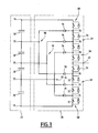
- the conversion system 10 comprises a set 22 of capacitors, a device 23 for balancing the voltage across at least one capacitor of the assembly, the balancing device 23 comprising a module 24 for balancing said voltage , P modules 26 for switching the DC input voltage, and means 27 for controlling each switching module 26.
- the balancing device 23 comprises a plurality of balancing modules 24 connected in parallel with the set of capacitors 22, such as, for example, a balancing module 24 for each switching module 26.
- the DC voltage source 12 has a direct DC input voltage V DC between the input terminals 16, 18 of the conversion system.
- the electric machine 14 is, for example, a three-phase electric motor.
- the electric motor 14 is, for example, a synchronous motor. In a variant, the motor 14 is an asynchronous motor.
- the set of capacitors 22, the balancing module 24 and the P switching modules 26 are electrically connected in parallel with each other between the two input terminals 16, 18. In other words, the two input terminals 16 , 18 are common to the set of capacitors 22, the balancing device 23 and the P switching modules 26. Each switching module 26 is also connected to a respective output terminal 20.
- the balancing module 24 is mechanically arranged between the set of capacitors 22 and the switching modules 26.
- the balancing module 24 is arranged mechanically between two switching modules 26.
- the switching modules 26 are arranged mechanically between the capacitor assembly 22 and the balancing module 24.
- the set of capacitors 22 comprises N-1 capacitors 28 connected in series between the two input terminals 16, 18 and interconnected by intermediate points 30.
- the capacitors 28 all have the same capacitor C.
- the capacitors 28 capacitors 28 have different capabilities.
- the 4 capacitors 28 are respectively denoted 28A, 28B, 28C, 28D successively from the negative input terminal 18 to the positive input terminal 16, the intermediate points being respectively denoted 30A, 30B, 30C.
- An end capacitor 28D is directly connected to the positive input terminal 16, and the other end capacitor 28A is directly connected to the negative input terminal 18.
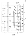
- the balancing module 24 comprises means 32 for determining the amount of electrical charges in excess or in default at each of the intermediate points 30, an element 34 for temporary storage of electrical energy, and means 36 for measuring the intensity of the current flowing in the temporary storage element.
- the balancing module 24 also comprises first current guiding means 40 capable of extracting electrical charges from an intermediate point 30 towards the temporary storage element 34, second current guiding means 42 capable of injecting electric charges. from the temporary storage element 34 to an intermediate point 30.
- the balancing module 24 also comprises a member 44 for controlling the first and second guide means 40, 42 capable of controlling the first guide means 40 so as to extract loads from at least one intermediate point 30 presenting an excess of charges and the second guide means 42 so as to inject the charges at at least one intermediate point 30 having a charge deficit.
- the determination means 32 comprise means for measuring the voltage at the input terminals 16, 18 and at each of the intermediate points 30A, 30B, 30C.
- the determining means 32 are, for example, voltmeters connected to the terminals of each of the capacitors 28.
- the temporary storage element 34 has a first terminal 45, a second terminal 46, and an electromagnetic coil 47 of inductance L disposed between the terminals 45, 46.
- the measuring means 36 are, for example, an ammeter connected in series with the temporary storage element 34.
- the first guide means 40 comprise N-1 switches 48 connected in series between the positive input terminal 16 and the first terminal 45 of the storage element, and N-1 diodes 50.
- the switches 48 are interconnected by connection points 52, two extreme switches of the N-1 switches 48 being directly connected to one of the two terminals of the positive terminal 16 and the first terminal 45 of the storage element.
- N-2 diodes 50 are connected directly between an intermediate point 30 and a respective connection point 52, and the last diode 50 is directly connected between the negative input terminal 18 and the first terminal 45 of the storage element .
- the 4 switches 48 are respectively denoted 48A, 48B, 48C, 48D successively from the positive input terminal 16 to the first terminal 45 of the storage element.
- the 4 diodes 50 are also marked 50A, 50B, 50C, 50D successively from the connection point 52 closest to the positive input terminal 16 to the first terminal 45 of the storage element. In other words, the last diode is denoted 50D.
- the connection points are also noted 52A, 52B, 52C successively from the positive terminal 16 to the first terminal 45 of the storage element.
- the second guide means 42 comprise N-1 switches 54 connected in series between the negative input terminal 18 and the second terminal 46 of the storage element, and N-1 diodes 56.
- the N-1 switches 54 are connected between they by connection points 58, two extreme switches of the N-1 switches being directly connected to one of the two terminals of the negative terminal 18 and the second terminal 46 of the storage element.
- N-2 diodes 56 are connected in reverse between an intermediate point 30 and a respective connection point 58, and the last diode 56 is connected in reverse between the positive input terminal 16 and the second terminal 46 of the storage element .
- the 4 switches 54 are respectively denoted 54A, 54B, 54C, 54D successively from the negative input terminal 18 to the second terminal 46 of the storage element.
- the 4 diodes 56 are denoted 56A, 56B, 56C, 56D successively from the connection point 58 closest to the negative terminal 18 to the second terminal 46 of the storage element.
- the three connection points 58 are noted 58A, 58B, 58C successively from the negative terminal 18 to the second terminal 46 of the storage element.
- the last diode is noted 56D.
- the switches 48, 54 of the first 40 and second 42 guide means are, for example, bidirectional in current and voltage.
- Each switch 48, 54 is a controllable electronic switch, and comprises, for example a transistor 60 and a diode 62 connected in antiparallel transistor.
- Transistor 60 is, for example, an IGBT (Insulated Gate Bipolar Transistor) transistor.
- the transistor 60 is a MOSFET (Metal Oxide Semiconductor Field Effect Transistor).
- each switch 48, 54 is a controllable electronic switch comprising a transistor, without the presence of a diode connected in antiparallel to the transistor.
- the controller 44 is connected to each of the controllable electronic switches 48, 54, and is able to send them respective control signals.
- the first terminal 45 of the temporary storage element is adapted to be connected to the positive terminal 16 via the first guide means 40, and the second terminal 46 of the storage element is able to be connected to the negative terminal 18 via the second guide means 42, until the establishment in the temporary storage element 34 of a current of value greater than a reference value I ref .
- the reference value I ref is, for example, substantially equal to the value of the current delivered by the respective phase of a switching module 26. In general, the reference value I ref is substantially equal to the value of the current flow. by an output phase of an electrical energy conversion device adapted to be connected to the input terminals 16, 18 and the intermediate points 30.
- the reference value I ref is, for example, a predetermined value.
- the reference value I ref predetermined is, for example, equal to 2000 A for a 10 MW conversion system having a voltage V DC equal to 5 kV between its input terminals 16,18.
- the balancing device 23 comprises means, not shown, for measuring a balancing cycle time TCm, and means, not shown, for calculating the reference value I ref as a function of the difference. between the measured cycle time TCm and a predefined cycle time value TC0.
- the predefined cycle time value TC0 is, for example, between 50 ⁇ s and 100 ms, preferably between 100 ⁇ s and 10 ms.
- the calculating means are suitable for increasing the reference value I ref when the difference between the measured cycle time TCm and the predefined cycle time value TC0 is positive, and for decreasing the reference value I ref when the difference between measured cycle time TCm and predefined cycle time value TC0 is negative, said reference value I ref being initially a predetermined value, for example equal to the value of the current that can be discharged by the respective phase of a switching module 26.
- the reference value I ref is not likely to be modified by the calculation means when the measured cycle time TCm is equal to the predefined cycle time value TC0.
- the value of the inductance L of the electromagnetic coil 47 of the temporary storage element 34 is substantially equal to the value of the DC voltage V DC between the input terminals 16, 18 multiplied by the minimum time of a cycle balancing, and divided by the reference value I ref .
- the value of the inductance L is preferably between 100 ⁇ H and 100 mH.
- the value of the inductance L is, for example, equal to 10 mH for a voltage V DC equal to 5 kV, a cycle time of 5 ms, and a reference value I ref equal to 2000 A.
- the value of the inductance L is, for example, equal to 300 ⁇ H for a voltage V DC equal to 6 kV, a cycle time of 100 ⁇ s, and a reference value I ref equal to 2000 A.
- the switching module 26 comprises two end branches 64 and N-2 intermediate branches 66.
- the switching module 26 has a topology of the type clamped by the neutral, also called topology NPC (English Neutral Point Clamped).
- Each end branch 64 is connected between a respective input terminal 16, 18 and the corresponding output terminal 20.
- Each end branch 64 comprises N-1 switches 68 connected in series and interconnected by mid-points 70.
- Each switch 68 is, for example, a bidirectional, bi-directional, controllable electronic switch in tension and comprises a transistor 72 and a diode 74 connected in antiparallel transistor.
- the transistor 72 is, for example, an IGBT transistor.
- Each intermediate branch 66 is connected to a respective intermediate point 30 of the capacitor set and comprises two diodes 76, 78.
- the first diode 76 is connected directly between said respective intermediate point 30 and a respective midpoint 70 of one of the two end branches 64, the second diode 78 being connected in reverse between said respective intermediate point 30 and a midpoint 70 of the other of the two end branches 64.
- the control member 44 starts by establishing a current I in the temporary storage element 34 until the value of said current I is equal to the reference value I ref , by controlling the closing of all the switches 48, 54 of the first 40 and second 42 guide means, in step 100.
- the first terminal 45 of the storage element is then connected to the positive terminal 16, and the second terminal 46 of the storage element is connected to the negative terminal 18.
- the measuring means 36 regularly measure the intensity of the current I flowing in the temporary storage element 34, and transmit this measurement of the current I to the control member 44 in order to determine the instant when the current reaches the reference value I ref , that is to say to determine the moment until the closing of all the switches 48, 54 must be controlled.
- the determination means 32 then measure, during the step 120, the voltage at each of the input terminals 16, 18 and at each of the intermediate points 30, also called the node j. , where j is an integer between 0 and 4.
- the node 0 corresponds to the negative terminal 18
- the nodes 1, 2, 3 respectively correspond to the intermediate points 30A, 30B, 30C
- the node 4 corresponds to the positive terminal 16.
- the variables ⁇ Q1, ⁇ Q2, ⁇ Q3 correspond respectively to the nodes 1, 2, 3, that is to say at the intermediate points 30A, 30B, 30C.
- the determination means 32 then determine the intermediate points 30 having an excess of electrical charges, the intermediate points 30 presenting a defect of electrical charges, as well as any intermediate points 30 whose voltage is balanced for which the variable ⁇ Qj is zero.
- the charges received by the temporary storage element 34 are injected at the intermediate points 30 in charge deficit during step 140.
- the determining means 32 also measure the voltage at the respective intermediate points, in order to determine the quantity of charges remaining in excess, respectively remaining in default, or to determine the moment when said respective intermediate points are in charge equilibrium in order to proceed to the next step.
- control member 44 sending control signals to switches 48, 54 to control switches 48, 54 in accordance with a predefined sequential law.
- the sequential law is such that, during the step of extracting charges 130, the diode of the first guide means 40 connected directly to the intermediate point in excess is passing, the switch or switches of the first means 40 arranged (s) between said passing diode of the first means and the storage element 34 being closed.
- the other switches of the first guide means 40 are open.
- the sequential law is also such that, during the charge injection step 140, the diode of the second guide means 42 connected in reverse to the intermediate point in deficit is passing, the second switch or switches 42 arranged (s) ) between the storage element 34 and the passing diode of the second means being closed.
- the other switches of the second guide means 42 are open.
- the sequential opening law of the switches is, for example, to open the switches in the following order 48A, 48B, 48C, 48D, respectively 54A, 54B, 54C, 54D.
- the instant of opening of the different switches 48, 54 depends on the quantity of charges to be transferred from or to the corresponding node.
- the sequential opening law of the switches is such that the opening of the second guide means 42 starts simultaneously with that of the first guide means 40.
- the sequential opening law of the switches is such that the opening of the second guide means 42 starts successively from that of the first guide means 40.
- the sequential opening law is the opening of the switches in the following order 54A, 54B, 54C, 54D, respectively 48A, 48B, 48C, 48D.
- the sequential opening law is in the following order 48A, 54A, then 48B, 54B, then 48C, 54C, then 48D, 54D.
- the sequential opening law is in the following order 54A, 48A, then 54B, 48B, then 54C, 48C, then 54D 48D.
- a measurement of the current I flowing in the temporary storage element 34 is performed by the measuring means 36 during the step 150. This measurement of current is transmitted to the control member 44.
- the controller 44 then compares the value of the measured current with the reference value I ref .
- a discharge of the temporary storage element 34 is then performed during the step 170 by the control member 44. which controls the opening of all the switches 48, 54. If the value of the current measured during the step 150 is on the contrary less than or equal to the reference value I ref , the control member 44 tests, during the step 175, if the value of the measured current is equal to the reference value I ref .
- the intermediate points 30 in excess of charges, as well as those in lack of charges, are again determined during step 120. Otherwise, that is to say if the value of the measured current is strictly lower. at the reference value I ref , then the control member 44 again controls the closing of all the switches 48, 54 until the establishment of a current in the temporary storage element 34 having a value intensity equal to the reference value I ref (step 100).
- the switches 48, 54 are, for example, controlled as described below.
- the control member 44 controls the opening of the switches 48A and 54A.
- This first state with the only switches 48A and 54A is of short duration and a function of the switching time of the switches 48A, 54A, since it is not necessary to extract charges from the intermediate point 30C or to inject charges to the intermediate point 30A.
- the control member 44 then controls the opening of the switches 48B and 54B, the switches 48A and 54A being always open.
- This second state is also of brief duration and a function of the switching time of the switches 48B, 54B, since it is not necessary to extract charges from the intermediate point 30B or to inject charges towards the intermediate point 30B. .
- the control member 44 then controls the opening of the switches 48C and 54C, the switches 48A, 48B, 54A and 54B are always open.
- the control member 44 finally controls the opening of the switches 48D and 54D, the switches 48A, 48B, 48C, 54A, 54B and 54C are always open.
- This state corresponds to a state of discharge of the temporary storage element 34, and is maintained only if the value of the current measured in the temporary storage element 34 is greater than the reference value I ref . If the value of the current measured in the temporary storage element 34 is on the contrary lower than the reference value I ref , then the discharge state is as short as possible and depends on the switching time of the 48D switches. and 54D from their open position to their closed position.
- the control member 44 controls the closing of the switches 48D and 54D for a short time if the intermediate points 30A and 30C are still in charge equilibrium. following the equilibration previously carried out, or for a necessary time the extraction of the excess charges, respectively the injection of the deficit charges, if the intermediate point 30A is again in excess of charges, respectively if the intermediate point 30C is again in deficit of charges.
- the control member 44 then controls the closing of the switches 48C and 54C for a short time, the switches 48D and 54D are always closed, then the closing of the switches 48B and 54B also for a short duration, the switches 48D, 48C, 54D and 54C still being closed, and finally closing switches 48A and 54A to return to the initial state where all switches 48, 54 are closed.
- the switches 48, 54 remain closed for a short time if the value of the current measured in the temporary storage element 34 is greater than or equal to the reference value I ref . If the value of the current measured in the temporary storage element 34 is on the contrary lower than the reference value I ref , then the closing state of the switches 48, 54 is of a duration corresponding to the time setting the current in the temporary storage element 34 to the reference value I ref .
- balancing the voltage across a corresponding capacitor is obtained in one cycle, corresponding to the successive execution of steps 100 to 150.
- the reference value I ref is a predetermined value.
- the reference value I ref is a function of the difference between the measured cycle time TCm and the predefined cycle time value TC0.
- the measured cycle time TCm is equal to the time interval between two successive test steps 175.
- the predefined cycle time value TC0 is, for example, between 50 ⁇ s and 100 ms, preferably between 100 ⁇ s and 10 ms.
- the method then further comprises a step, not shown, of calculating the reference value I ref .
- the reference value I ref is increased when the difference between the measured cycle time TCm and the predefined cycle time value TC0 is positive, and the reference value I ref is decreased when the difference between the measured cycle time TCm and the predefined cycle time value TC0 is negative.
- the reference value I ref is not changed when the measured cycle time TCm is equal to the predefined cycle time value TC0.
- the method further comprises a timing step, not shown, during which the intermediate point from which the charges are extracted during the extraction step 130 is identical to the intermediate point to which the charges are injected. during the injection step 140, the extraction step 130 and the injection step 140 being performed simultaneously.
- the delay step thus makes it possible to modify the value of the measured cycle time TCm.
- the reference value I ref is slaved as a function of the value of the measured cycle time TCm, this value being itself controllable via the timing step.
- the balancing device thus makes it possible to balance the voltage across each of the capacitors connected between the input terminals, whatever the voltage and the current delivered by the conversion device to be connected between the terminals. input.
- FIG 5 illustrates a second embodiment of the invention for which elements similar to the first embodiment, described above, are identified by identical references, and are therefore not described again.
- the first guide means 40 comprise N-1 switches 180 connected in parallel between the first terminal 45 of the storage element and one of the positive input terminal 16 and the intermediate points 30, and N-1 diodes 182.
- N-2 diodes 182 are connected in series with said switches 180 connected between the first terminal 45 of the storage element and the intermediate points 30 and in direct contact between the intermediate points 30 and the first terminal 45
- the last diode 182 is directly connected between the negative input terminal 18 and the first terminal 45 of the storage element.
- the 4 switches 180 are respectively denoted 180A, 180B, 180C, 180D successively from the positive input terminal 16 to the first terminal 45 of the storage element.
- the four diodes 182 are also denoted 182A, 182B, 182C, 182D successively from the intermediate point 30C to the negative input terminal 18. The last diode is noted 182D.
- the second guide means 42 comprise N-1 switches 190 connected in parallel between the second terminal 46 of the storage element and one of the input negative terminal 18 and the intermediate points 30, and N-1 diodes 192.
- N-2 diodes 192 are connected in series with said switches 190 connected between the second terminal 46 of the storage element and the intermediate points 30 and in reverse between the intermediate points 30 and the second terminal 46.
- the last diode 192 is connected in reverse between the positive input terminal 16 and the second terminal 46 of the storage element.
- the 4 switches 190 are respectively marked 190A, 190B, 190C, 190D successively from the negative input terminal 18 to the second terminal 46 of the storage element.
- the 4 diodes 192 are denoted 192A, 192B, 192C, 192D successively from the intermediate point 30A to the positive input terminal 16.
- the last diode is denoted 192D.
- the switches 180, 190 of the first 40 and second 42 guide means are, for example, bidirectional in current and voltage.
- Each switch 180, 190 is a controllable electronic switch, and comprises, for example a transistor 60 and a diode 62 connected in antiparallel transistor.
- Transistor 60 is, for example, an IGBT (Insulated Gate Bipolar Transistor) transistor.
- the Transistor 60 is a MOSFET (Metal Oxide Semiconductor Field Effect Transistor).
- each switch 180, 190 is a controllable electronic switch having a transistor, without the presence of a diode connected antiparallel transistor.
- the controller 44 is connected to each of the controllable electronic switches 180, 190, and is able to send them respective control signals.
- FIG 6 illustrates a third embodiment of the invention for which elements similar to the first embodiment, described above, are identified by identical references, and are therefore not described again.
- the switching module 26 has a topology of the type controlled by the neutral, also called NPP (Neutral Point Piloted) topology.
- NPP Neutral Point Piloted
- the switching module 26 then comprises two end branches 200 and N-2 intermediate branches 202.
- Each end branch 200 is connected between a respective input terminal 16, 18 and the corresponding output terminal 20, and comprises a controllable electronic switch 204 .
- Each intermediate branch 202 is connected between a respective intermediate point 30 of the capacitor set and said output terminal 20, and comprises two switches 206, 208 connected in anti-series.
- Each switch 204, 206, 208 is, for example, a bidirectional bidirectional electronic switch in current and voltage, comprising a transistor 210 and a diode 212 connected in antiparallel of the transistor.
- the transistor 210 is, for example, an IGBT transistor.
- this third embodiment is identical with respect to the balancing device 23 to that of the first embodiment, and is therefore not described again.
- the balancing device makes it possible to balance the voltage across each of the capacitors of the set of capacitors, whatever the voltage and the current delivered by the conversion device to be connected between the capacitors. input terminals.
Landscapes
- Engineering & Computer Science (AREA)
- Power Engineering (AREA)
- Inverter Devices (AREA)
- Rectifiers (AREA)
- Charge And Discharge Circuits For Batteries Or The Like (AREA)
- Dc-Dc Converters (AREA)
Description
La présente invention concerne un dispositif d'équilibrage de la tension aux bornes d'au moins un condensateur d'un ensemble de condensateurs, ledit ensemble de condensateurs comprenant une borne positive d'entrée, une borne négative d'entrée, N-1 condensateurs connectés en série entre les deux bornes d'entrée et reliés entre eux par des points intermédiaires, deux condensateurs extrémaux des N-1 condensateurs étant directement reliés à l'une des deux bornes d'entrée, N étant supérieur ou égal à 3, les deux bornes d'entrée et les points intermédiaires étant propres à être connectés à un dispositif de conversion d'énergie électrique susceptible de provoquer un déséquilibre de la tension aux bornes d'au moins un condensateur.The present invention relates to a device for balancing the voltage across at least one capacitor of a set of capacitors, said set of capacitors comprising a positive input terminal, a negative input terminal, N-1 capacitors connected in series between the two input terminals and interconnected by intermediate points, two extreme capacitors of the N-1 capacitors being directly connected to one of the two input terminals, N being greater than or equal to 3, the two input terminals and intermediate points being adapted to be connected to an electrical energy conversion device capable of causing an unbalance of the voltage across at least one capacitor.
L'invention concerne également un système de conversion de tension comprenant un tel dispositif d'équilibrage.The invention also relates to a voltage conversion system comprising such a balancing device.
L'invention concerne également un procédé d'équilibrage de la tension aux bornes d'un condensateur d'un ensemble de condensateurs.The invention also relates to a method for balancing the voltage across a capacitor of a set of capacitors.
On connaît un onduleur de tension à trois niveaux comprenant une borne positive d'entrée, une borne négative d'entrée et une borne de sortie pour la ou chaque phase du courant alternatif délivré en sortie de l'onduleur, et deux condensateurs connectés en série entre la borne positive et la borne négative, les deux condensateurs étant reliés entre eux par un point milieu. L'onduleur comprend, pour chaque borne de sortie, un module de commutation de la tension continue d'entrée, chaque module de commutation étant connecté entre les deux bornes d'entrée et la borne de sortie respective. Lorsque la tension et le courant en sortie de l'onduleur sont symétriques par rapport au point milieu, le bilan des charges électriques au point milieu est nul sur une période du courant alternatif.There is known a three-level voltage inverter comprising a positive input terminal, a negative input terminal and an output terminal for the or each phase of the AC current delivered at the output of the inverter, and two capacitors connected in series. between the positive terminal and the negative terminal, the two capacitors being connected to each other by a midpoint. The inverter comprises, for each output terminal, a switching module of the input DC voltage, each switching module being connected between the two input terminals and the respective output terminal. When the voltage and the output current of the inverter are symmetrical with respect to the midpoint, the balance of the electric charges at the midpoint is zero over a period of the alternating current.
Toutefois, la valeur de la capacité des condensateurs doit être suffisamment élevée afin de limiter la variation de tension au point milieu au cours d'une période du courant alternatif, ce qui engendre l'utilisation de condensateurs d'encombrement et de coût importants, lorsque le courant alternatif de sortie est un courant à basse fréquence.However, the capacitance value of the capacitors must be high enough to limit the voltage variation at the mid-point during a period of alternating current, which leads to the use of capacitors of large size and cost, when the output AC current is a low frequency current.
On connaît également un onduleur de tension à N niveaux, où N est un nombre entier supérieur à trois, comprenant une borne positive d'entrée, une borne négative d'entrée, une borne de sortie pour la ou chaque phase du courant alternatif de sortie, et un ensemble de condensateurs comportant N-1 condensateurs connectés en série entre les deux bornes d'entrée et reliés entre eux par des points intermédiaires, deux condensateurs extrémaux des N-1 condensateurs étant directement reliés à l'une des deux bornes d'entrée. L'onduleur de tension à N niveaux comprend, pour chaque borne de sortie, un module de commutation de la tension continue d'entrée, chaque module de commutation étant connecté entre les deux bornes d'entrée et la borne de sortie respective. L'onduleur de tension à N niveaux comprend également des moyens d'équilibrage de la tension aux bornes de chacun des N-1 condensateurs par ajout d'une composante homopolaire de mode commun sur chacune des phases du courant alternatif de sortie, le décalage entre les phases permettant de charger ou de décharger les condensateurs.There is also known an N-level voltage inverter, where N is an integer greater than three, comprising a positive input terminal, an input negative terminal, an output terminal for the or each output AC phase. , and a set of capacitors having N-1 capacitors connected in series between the two input terminals and interconnected by intermediate points, two extreme capacitors of the N-1 capacitors being directly connected to one of the two input terminals. The N-level voltage inverter comprises, for each output terminal, a switching module of the input DC voltage, each switching module being connected between the two input terminals and the respective output terminal. The N-level voltage inverter also comprises means for balancing the voltage at the terminals of each of the N-1 capacitors by adding a common-mode zero-sequence component on each of the phases of the output AC current, the offset between the phases for charging or discharging the capacitors.
Toutefois, de tels moyens d'équilibrage sont efficaces lorsque l'amplitude de la tension alternative de sortie est inférieure à une valeur limite sensiblement égale au quart de la valeur de la tension continue d'entrée. Les moyens d'équilibrage ne permettent pas d'équilibrer correctement les charges électriques aux bornes desdits condensateurs lorsque l'amplitude du courant alternatif de sortie est supérieure à la valeur limite précitée, alors que l'intérêt des onduleurs de tension multi-niveaux est de délivrer un courant alternatif présentant une amplitude en tension élevée. Autres dispositifs d'équilibrage sont connus de
Le but de l'invention est de proposer un dispositif d'équilibrage permettant d'équilibrer la tension en chacun des points intermédiaires de l'ensemble de condensateurs quelle que soit la tension et le courant délivré par le dispositif de conversion propre à être connecté entre les bornes d'entrée.The object of the invention is to provide a balancing device for balancing the voltage at each of the intermediate points of the capacitor set regardless of the voltage and the current delivered by the conversion device to be connected between the input terminals.
A cet effet, l'invention a pour objet un dispositif d'équilibrage du type précité, caractérisé en ce que qu'il comprend au moins un module d'équilibrage de la tension aux bornes de chacun des N-1 condensateurs, le module d'équilibrage étant connecté entre les deux bornes d'entrée et comportant des moyens de détermination de la quantité de charges en excès ou en défaut en chacun des points intermédiaires, un élément de stockage temporaire d'énergie électrique comportant deux bornes, des premiers moyens de guidage de courant propres à extraire des charges électriques depuis un point intermédiaire vers une borne de l'élément de stockage temporaire, des seconds moyens de guidage de courant propres à injecter des charges électriques depuis l'autre borne de l'élément de stockage temporaire vers un point intermédiaire, et un organe de commande des premiers et seconds moyens de guidage propre à commander les premiers moyens de guidage de manière à extraire des charges d'au moins un point intermédiaire présentant un excès de charges et les seconds moyens de guidage de manière à injecter les charges à au moins un point intermédiaire présentant un déficit de charges, et
en ce qu'une borne de l'élément de stockage temporaire est propre à être connectée à la borne positive d'entrée, respectivement à la borne négative d'entrée , via les premiers moyens de guidage et l'autre borne de l'élément de stockage temporaire est propre à être connectée à la borne négative d'entrée, respectivement à la borne positive d'entrée, via les seconds moyens de guidage, pour accroître, respectivement réduire, l'énergie stockée dans l'élément de stockage temporaire.For this purpose, the subject of the invention is a balancing device of the aforementioned type, characterized in that it comprises at least one module for balancing the voltage at the terminals of each of the N-1 capacitors, the module for balancing being connected between the two input terminals and having means for determining the amount of excess or fault charges at each of the intermediate points, a temporary storage element of electrical energy comprising two terminals, first means of current guiding adapted to extract electric charges from an intermediate point to a terminal of the temporary storage element, second current guiding means adapted to inject electric charges from the other terminal of the temporary storage element to an intermediate point, and a control member of the first and second guide means adapted to control the first guiding means so as to extract c harassing at least one intermediate point presenting an excess of charges and the second guiding means so as to inject the charges at at least one intermediate point presenting a deficit of charges, and
in that a terminal of the temporary storage element is adapted to be connected to the positive input terminal, respectively to the negative input terminal, via the first guide means and the other terminal of the temporary storage element is adapted to be connected to the negative input terminal, respectively to the positive input terminal, via the second guide means, for increasing, respectively reduce, the energy stored in the temporary storage element.
Suivant d'autres modes de réalisation, le dispositif d'équilibrage comprend une ou plusieurs des caractéristiques suivantes, prises isolément ou suivant toutes les combinaisons techniquement possibles :
- l'élément de stockage temporaire comporte au moins une bobine électromagnétique,
- chacun des premiers et seconds moyens de guidage comporte N-1 interrupteurs et N-1 diodes,
- les interrupteurs des premiers moyens sont connectés en série entre la borne positive d'entrée et une borne de l'élément de stockage, et reliés entre eux par des points de connexion, deux interrupteurs extrémaux des N-1 interrupteurs étant directement reliés à l'une des deux bornes parmi la borne positive et la borne de l'élément de stockage, N-2 diodes des premiers moyens sont connectées en direct entre un point intermédiaire respectif et un point de connexion respectif des premiers moyens, et l'autre diode des premiers moyens est connectée en direct entre la borne négative d'entrée et la borne de l'élément de stockage, et
les interrupteurs des seconds moyens sont connectés en série entre la borne négative d'entrée et l'autre borne de l'élément de stockage, et reliés entre eux par des points de connexion, deux interrupteurs extrémaux des N-1 interrupteurs étant directement reliés à l'une des deux bornes parmi la borne négative et l'autre borne de l'élément de stockage, N-2 diodes des seconds moyens sont connectées en inverse entre un point intermédiaire respectif et un point de connexion respectif des seconds moyens, et l'autre diode des seconds moyens est connectée en inverse entre la borne positive d'entrée et l'autre borne de l'élément de stockage, - les interrupteurs des premiers moyens sont connectés en parallèle entre la borne de l'élément de stockage et un point parmi la borne positive d'entrée et les points intermédiaires, N-2 diodes des premiers moyens sont connectées en série avec lesdits interrupteurs connectés entre la borne de l'élément de stockage et les points intermédiaires et en direct entre les points intermédiaires et la borne, et l'autre diode des premiers moyens est connectée en direct entre la borne négative d'entrée et la borne de l'élément de stockage, et
les interrupteurs des seconds moyens sont connectés en parallèle entre l'autre borne de l'élément de stockage et un point parmi la borne négative d'entrée et les points intermédiaires , N-2 diodes des seconds moyens sont connectées en série avec lesdits interrupteurs connectés entre l'autre borne de l'élément de stockage et les points intermédiaires et en inverse entre les points intermédiaires et l'autre borne, et l'autre diode des seconds moyens est connectée en inverse entre la borne positive d'entrée et l'autre borne de l'élément de stockage, - les moyens de détermination de la quantité de charges en excès ou en défaut comportent des moyens de mesure de la tension aux bornes d'entrée et en chacun des points intermédiaires.
- the temporary storage element comprises at least one electromagnetic coil,
- each of the first and second guiding means comprises N-1 switches and N-1 diodes,
- the switches of the first means are connected in series between the positive input terminal and a terminal of the storage element, and connected to each other by connection points, two extreme switches of the N-1 switches being directly connected to the one of the two terminals among the positive terminal and the terminal of the storage element, N-2 diodes of the first means are directly connected between a respective intermediate point and a respective connection point of the first means, and the other diode of first means is connected directly between the negative input terminal and the terminal of the storage element, and
the switches of the second means are connected in series between the negative input terminal and the other terminal of the storage element, and interconnected by connection points, two extreme switches of the N-1 switches being directly connected to one of the two terminals among the negative terminal and the other terminal of the storage element, N-2 diodes of the second means are connected in reverse between a respective intermediate point and a respective connection point of the second means, and another diode of the second means is reverse connected between the positive input terminal and the other terminal of the storage element, - the switches of the first means are connected in parallel between the terminal of the storage element and a point among the positive input terminal and the intermediate points, N-2 diodes of the first means are connected in series with said switches connected between the terminal of the storage element and the intermediate and direct points between the intermediate points and the terminal, and the other diode of the first means is connected directly between the negative input terminal and the terminal of the storage element , and
the switches of the second means are connected in parallel between the other terminal of the storage element and one of the negative input terminal and the points intermediate, N-2 diodes of the second means are connected in series with said switches connected between the other terminal of the storage element and the intermediate points and in reverse between the intermediate points and the other terminal, and the other diode second means is reverse connected between the positive input terminal and the other terminal of the storage element, - the means for determining the quantity of charges in excess or in default comprise means for measuring the voltage at the input terminals and at each of the intermediate points.
L'invention a également pour objet un système de conversion d'une tension continue d'entrée en une tension alternative de sortie comportant au moins une phase, du type comprenant,
- une borne positive d'entrée, une borne négative d'entrée, et une borne de sortie pour la ou chaque phase,
- un ensemble de condensateurs comportant N-1 condensateurs connectés en série entre les deux bornes d'entrée et reliés entre eux par des points intermédiaires, deux condensateurs extrémaux des N-1 condensateurs étant directement reliés à l'une des deux bornes d'entrée, N étant supérieur ou égal à 3,
- pour chaque borne de sortie, un module de commutation de la tension continue d'entrée, chaque module de commutation étant connecté entre les deux bornes d'entrée et la borne de sortie respective, et étant propre à convertir la tension continue d'entrée en la phase respective de la tension alternative de sortie,
- des moyens de commande de chaque module de commutation,
- a positive input terminal, a negative input terminal, and an output terminal for the or each phase,
- a set of capacitors comprising N-1 capacitors connected in series between the two input terminals and interconnected by intermediate points, two extreme capacitors of the N-1 capacitors being directly connected to one of the two input terminals, N being greater than or equal to 3,
- for each output terminal, a switching module of the input DC voltage, each switching module being connected between the two input terminals and the respective output terminal, and being able to convert the DC input voltage into the respective phase of the output AC voltage,
- control means for each switching module,
Suivant d'autres modes de réalisation, le système de conversion comprend une ou plusieurs des caractéristiques suivantes, prises isolément ou suivant toutes les combinaisons techniquement possibles :
- le module de commutation comprend deux branches extrêmes et N-2 branches intermédiaires, chaque branche extrême est connectée entre une borne d'entrée respective et ladite borne de sortie, et comporte N-1 interrupteurs connectés en série et reliés entre eux par des points milieux, et chaque branche intermédiaire est connectée à un point intermédiaire respectif et comporte deux diodes, la première diode étant connectée en direct entre ledit point intermédiaire respectif et un point milieu respectif d'une des deux branches extrêmes , et la seconde diode étant connectée en inverse entre ledit point intermédiaire respectif et un point milieu respectif de l'autre des deux branches extrêmes,
- le module de commutation comprend deux branches extrêmes et N-2 branches intermédiaires, chaque branche extrême comporte un interrupteur connecté entre une borne d'entrée respective et ladite borne de sortie, et chaque branche intermédiaire comporte deux interrupteurs connectés en anti-série entre un point intermédiaire respectif et ladite borne de sortie.
- the switching module comprises two end branches and N-2 intermediate branches, each end branch is connected between a respective input terminal and said output terminal, and has N-1 switches connected in series and interconnected by midpoints. , and each intermediate branch is connected to a respective intermediate point and comprises two diodes, the first diode being connected directly between said respective intermediate point and a respective midpoint of one of the two extreme branches, and the second diode being connected in reverse enter said respective intermediate point and a respective midpoint of the other of the two extreme branches,
- the switching module comprises two extreme branches and N-2 intermediate branches, each extreme branch comprises a switch connected between a respective input terminal and said output terminal, and each intermediate branch comprises two switches connected anti-series between a point respective intermediate and said output terminal.
L'invention a également pour objet un procédé d'équilibrage de la tension aux bornes d'un condensateur d'un ensemble de condensateurs, par l'intermédiaire d'un dispositif d'équilibrage de ladite tension,
ledit ensemble de condensateurs comprenant une borne positive d'entrée, une borne négative d'entrée, N-1 condensateurs connectés en série entre les deux bornes d'entrée et reliés entre eux par des points intermédiaires, deux condensateurs extrémaux des N-1 condensateurs étant directement reliés à l'une des deux bornes d'entrée, N étant supérieur ou égal à 3, les deux bornes d'entrée et les points intermédiaires étant propres à être connectés à un dispositif de conversion d'énergie électrique susceptible de provoquer un déséquilibre de la tension aux bornes d'au moins un condensateur,
le dispositif d'équilibrage comprenant au moins un module d'équilibrage connecté entre les deux bornes d'entrée et comportant des moyens de détermination de la quantité de charges en excès ou en défaut en chacun des points intermédiaires, un élément de stockage temporaire d'énergie électrique comportant deux bornes, des premiers moyens de guidage de courant propres à extraire des charges électriques depuis un point intermédiaire vers une borne de l'élément de stockage temporaire, et des seconds moyens de guidage de courant propres à injecter des charges électriques depuis l'autre borne de l'élément de stockage temporaire vers un point intermédiaire,
le procédé comprenant :
- une étape d'établissement d'un courant dans l'élément de stockage temporaire jusqu'à ce que la valeur dudit courant soit supérieure à une valeur de référence, au cours de laquelle une borne de l'élément de stockage temporaire est connectée à la borne positive d'entrée via une commande correspondante des premiers moyens de guidage, l'autre borne de l'élément de stockage temporaire étant connectée à la borne négative d'entrée via une commande correspondante des seconds moyens de guidage ,
- une étape de détermination d'un point intermédiaire en excès de charges électriques et/ou d'un autre point intermédiaire en défaut de charges électriques,
- une étape d'extraction de charges du point intermédiaire en excès de charges à destination de l'élément de stockage temporaire, via une commande correspondante des premiers moyens de guidage, et/ou
- une étape d'injection de charges au point intermédiaire en défaut de charges depuis de l'élément de stockage temporaire, via une commande correspondante des seconds moyens de guidage,
- une étape de mesure du courant dans l'élément de stockage temporaire à l'issue d'au moins une étape d'extraction et/ou d'injection de charges, et
- une étape de décharge de l'élément de stockage temporaire lorsque la valeur du courant mesuré lors de l'étape de mesure est supérieure à celle de la valeur de référence.
said capacitor set comprising a positive input terminal, a negative input terminal, N-1 capacitors connected in series between the two input terminals and interconnected by intermediate points, two extreme capacitors of the N-1 capacitors being directly connected to one of the two input terminals, N being greater than or equal to 3, the two input terminals and the intermediate points being adapted to be connected to an electrical energy conversion device capable of causing a unbalance of the voltage across at least one capacitor,
the balancing device comprising at least one balancing module connected between the two input terminals and having means for determining the amount of excess or fault charges at each of the intermediate points, a temporary storage element of electrical energy having two terminals, first current guiding means adapted to extract electrical charges from an intermediate point to a terminal of the temporary storage element, and second current guiding means adapted to inject electric charges from the another terminal of the temporary storage element to an intermediate point,
the method comprising:
- a step of setting a current in the temporary storage element until the value of said current is greater than a reference value, during which a terminal of the temporary storage element is connected to the positive input terminal via a corresponding command of the first guide means, the other terminal of the temporary storage element being connected to the negative input terminal via a corresponding command of the second guide means,
- a step of determining an intermediate point in excess of electrical charges and / or another intermediate point in the absence of electrical charges,
- a step of extracting charges from the intermediate point in excess of charges to the temporary storage element, via a corresponding command of the first guide means, and / or
- a step of injecting charges at the intermediate point in the absence of charges from the temporary storage element, via a corresponding command of the second guide means,
- a step of measuring the current in the temporary storage element after at least one extraction and / or charge injection step, and
- a step of discharging the temporary storage element when the value of the current measured during the measuring step is greater than that of the reference value.
Suivant d'autres modes de réalisation, le procédé d'équilibrage comprend une ou plusieurs des caractéristiques suivantes, prises isolément ou suivant toutes les combinaisons techniquement possibles :
- chacun des premiers et seconds moyens de guidage comporte N-1 interrupteurs et N-1 diodes,
les interrupteurs des premiers moyens étant connectés en série entre la borne positive d'entrée et une borne de l'élément de stockage, et reliés entre eux par des points de connexion, deux interrupteurs extrémaux des N-1 interrupteurs étant directement reliés à l'une des deux bornes parmi la borne positive et la borne de l'élément de stockage, N-2 diodes des premiers moyens étant connectées en direct entre un point intermédiaire respectif et un point de connexion respectif des premiers moyens, et l'autre diode des premiers moyens étant connectée en direct entre la borne négative d'entrée et la borne de l'élément de stockage,
les interrupteurs des seconds moyens étant connectés en série entre la borne négative d'entrée et l'autre borne de l'élément de stockage, et reliés entre eux par des points de connexion, deux interrupteurs extrémaux des N-1 interrupteurs étant directement reliés à l'une des deux bornes parmi la borne négative et l'autre borne de l'élément de stockage, N-2 diodes des seconds moyens étant connectées en inverse entre un point intermédiaire respectif et un point de connexion respectif des seconds moyens, et l'autre diode des seconds moyens étant connectée en inverse entre la borne positive d'entrée et l'autre borne de l'élément de stockage,
lors de l'étape initiale d'établissement du courant dans l'élément de stockage temporaire, tous les interrupteurs des premiers et seconds moyens de guidage sont fermés,
lors de l'étape d'extraction de charges, la diode des premiers moyens de guidage connectée en direct au point intermédiaire en excès de charges est passante, le ou les interrupteurs des premiers moyens disposés entre ladite diode passante des premiers moyens et l'élément de stockage étant fermés, les autres interrupteurs des premiers et seconds moyens de guidage étant ouverts,
lors de l'étape d'injection de charges, la diode des seconds moyens de guidage connectée en inverse au point intermédiaire en défaut de charges est passante, le ou les interrupteurs des seconds moyens disposés entre l'élément de stockage et ladite diode passante des seconds moyens étant fermés, les autres interrupteurs des premiers et seconds moyens de guidage étant ouverts, et
lors de l'étape de décharge de l'élément de stockage, tous les interrupteurs des premiers et seconds moyens de guidage sont ouverts, - la valeur de référence est une valeur prédéterminée,
- le procédé comprend en outre une étape de mesure d'un temps de cycle d'équilibrage, et la valeur de référence est fonction de la différence entre le temps de cycle mesuré et une valeur de temps de cycle prédéfinie,
- la valeur de référence est augmentée lorsque la différence entre le temps de cycle mesuré et la valeur de temps de cycle prédéfinie est positive, la valeur de référence est conservée lorsque la différence entre le temps de cycle mesuré et la valeur de temps de cycle prédéfinie est nulle, et la valeur de référence est diminuée lorsque la différence entre le temps de cycle mesuré et la valeur de temps de cycle prédéfinie est négative,
- le procédé comprend en outre une étape de temporisation, au cours de laquelle le point intermédiaire à partir duquel sont extraites les charges lors de l'étape d'extraction est identique au point intermédiaire vers lequel les charges sont injectées lors de l'étape d'injection, l'étape l'extraction et l'étape d'injection étant effectuées simultanément.
- each of the first and second guiding means comprises N-1 switches and N-1 diodes,
the switches of the first means being connected in series between the positive input terminal and a terminal of the storage element, and interconnected by connection points, two extreme switches of the N-1 switches being directly connected to the one of the two terminals among the positive terminal and the terminal of the storage element, N-2 diodes of the first means being directly connected between a respective intermediate point and a respective connection point of the first means, and the other diode of first means being directly connected between the negative input terminal and the terminal of the storage element,
the switches of the second means being connected in series between the negative input terminal and the other terminal of the storage element, and interconnected by connection points, two extreme switches of the N-1 switches being directly connected to one of the two terminals among the negative terminal and the other terminal of the storage element, N-2 diodes of the second means being connected in reverse between a respective intermediate point and a respective connection point of the second means, and another diode of the second means being connected in reverse between the positive input terminal and the other terminal of the storage element,
during the initial step of establishing the current in the temporary storage element, all the switches of the first and second guide means are closed,
during the step of extracting charges, the diode of the first guide means connected directly to the intermediate point in excess of charges is passing, the one or more switches of the first means disposed between said passing diode of the first means and the storage element being closed, the other switches of the first and second guiding means being open,
during the charge injection step, the diode of the second guide means connected in reverse to the intermediate point in charge defect is passing, the second or second switches disposed between the storage element and said pass diode of second means being closed, the other switches of the first and second guiding means being open, and
during the step of discharging the storage element, all the switches of the first and second guiding means are open, - the reference value is a predetermined value,
- the method further comprises a step of measuring a balancing cycle time, and the reference value is a function of the difference between the measured cycle time and a predefined cycle time value,
- the reference value is increased when the difference between the measured cycle time and the predefined cycle time value is positive, the reference value is retained when the difference between the measured cycle time and the predefined cycle time value is zero, and the reference value is decreased when the difference between the measured cycle time and the predefined cycle time value is negative,
- the method further comprises a delay step, during which the intermediate point from which the charges are extracted during the extraction step is identical to the intermediate point to which the charges are injected during the step of injection, the extraction step and the injection step being performed simultaneously.
Ces caractéristiques et avantages de l'invention apparaîtront à la lecture de la description qui va suivre, donnée uniquement à titre d'exemple, et faite en référence aux dessins annexés, sur lesquels :
- la
figure 1 est une représentation schématique d'un système de conversion selon l'invention ; - la
figure 2 est un schéma électrique d'un module d'équilibrage de la tension aux bornes de condensateurs du système de conversion de lafigure 1 ; - la
figure 3 est un schéma électrique d'un module de commutation de la tension continue d'entrée du système de conversion de lafigure 1 ; - la
figure 4 est un organigramme du procédé d'équilibrage selon l'invention, - la
figure 5 est un schéma électrique analogue à celui de lafigure 2 selon un deuxième mode de réalisation de l'invention ; et - la
figure 6 est un schéma électrique analogue à celui de lafigure 3 selon un troisième mode de réalisation de l'invention.
- the
figure 1 is a schematic representation of a conversion system according to the invention; - the
figure 2 is a circuit diagram of a module for balancing the voltage across the capacitors of the conversion system of thefigure 1 ; - the
figure 3 is a circuit diagram of a switching module of the DC input voltage of the conversion system of thefigure 1 ; - the
figure 4 is a flowchart of the balancing method according to the invention, - the
figure 5 is a circuit diagram similar to that of thefigure 2 according to a second embodiment of the invention; and - the
figure 6 is a circuit diagram similar to that of thefigure 3 according to a third embodiment of the invention.
Sur la
Le système de conversion 10 comprend une borne positive d'entrée 16, une borne négative d'entrée 18, et une borne de sortie 20 pour chacune des P phases. P est un nombre entier supérieur ou égal à 1. Dans l'exemple de réalisation de la
Le système de conversion 10 comprend un ensemble 22 de condensateurs, un dispositif 23 d'équilibrage de la tension aux bornes d'au moins un condensateur de l'ensemble, le dispositif d'équilibrage 23 comportant un module 24 d'équilibrage de ladite tension, P modules 26 de commutation de la tension continue d'entrée, et des moyens 27 de commande de chaque module de commutation 26.The
En variante, le dispositif d'équilibrage 23 comprend plusieurs modules d'équilibrage 24 connectés en parallèle de l'ensemble de condensateurs 22, tel que par exemple un module d'équilibrage 24 pour chaque module de commutation 26.In a variant, the balancing
La source de tension continue 12 présente une tension continue d'entrée VDC entre les bornes d'entrée 16, 18 du système de conversion.The
La machine électrique 14 est, par exemple, un moteur électrique triphasé. Le moteur électrique 14 est, par exemple, un moteur synchrone. En variante, le moteur 14 est un moteur asynchrone.The
L'ensemble de condensateurs 22, le module d'équilibrage 24 et les P modules de commutation 26 sont électriquement connectés en parallèle les uns des autres entre les deux bornes d'entrée 16, 18. Autrement dit, les deux bornes d'entrée 16, 18 sont communes à l'ensemble de condensateurs 22, au dispositif d'équilibrage 23 et aux P modules de commutation 26. Chaque module de commutation 26 est également connecté à une borne de sortie 20 respective.The set of
Dans l'exemple de réalisation de la
En variante, le module d'équilibrage 24 est agencé mécaniquement entre deux modules de commutation 26. En variante encore, les modules de commutation 26 sont agencés mécaniquement entre l'ensemble de condensateurs 22 et le module d'équilibrage 24.In a variant, the
Sur la
Dans l'exemple de réalisation de la
Un condensateur extrémal 28D est directement relié à la borne positive d'entrée 16, et l'autre condensateur extrémal 28A est directement relié à la borne négative d'entrée 18.An
Le module d'équilibrage 24 comporte des moyens 32 de détermination de la quantité de charges électriques en excès ou en défaut en chacun des points intermédiaires 30, un élément 34 de stockage temporaire d'énergie électrique, et des moyens 36 de mesure de l'intensité du courant circulant dans l'élément de stockage temporaire. Le module d'équilibrage 24 comporte également des premiers moyens 40 de guidage de courant propres à extraire des charges électriques depuis un point intermédiaire 30 vers l'élément de stockage temporaire 34, des seconds moyens 42 de guidage de courant propres à injecter des charges électriques depuis l'élément de stockage temporaire 34 vers un point intermédiaire 30.The
Le module d'équilibrage 24 comporte également un organe 44 de commande des premiers et seconds moyens de guidage 40, 42 propre à commander les premiers moyens de guidage 40 de manière à extraire des charges d'au moins un point intermédiaire 30 présentant un excès de charges et les seconds moyens de guidage 42 de manière à injecter les charges à au moins un point intermédiaire 30 présentant un déficit de charges.The
Les moyens de détermination 32 comportent des moyens de mesure de la tension aux bornes d'entrées 16,18 et en chacun des points intermédiaires 30A, 30B, 30C. Les moyens de détermination 32 sont, par exemple, des voltmètres connectés aux bornes de chacun des condensateurs 28.The determination means 32 comprise means for measuring the voltage at the
L'élément de stockage temporaire 34 comporte une première borne 45, une deuxième borne 46, et une bobine électromagnétique 47 d'inductance L disposée entre les bornes 45, 46.The
Les moyens de mesure 36 sont, par exemple, un ampèremètre connecté en série de l'élément de stockage temporaire 34.The measuring means 36 are, for example, an ammeter connected in series with the
Les premiers moyens de guidage 40 comportent N-1 interrupteurs 48 connectés en série entre la borne positive d'entrée 16 et la première borne 45 de l'élément de stockage, et N-1 diodes 50. Les interrupteurs 48 sont reliés entre eux par des points de connexion 52, deux interrupteurs extrémaux des N-1 interrupteurs 48 étant directement reliés à l'une des deux bornes parmi la borne positive 16 et la première borne 45 de l'élément de stockage. N-2 diodes 50 sont connectées en direct entre un point intermédiaire 30 et un point de connexion 52 respectif, et la dernière diode 50 est connectée en direct entre la borne négative d'entrée 18 et la première borne 45 de l'élément de stockage.The first guide means 40 comprise N-1 switches 48 connected in series between the
Dans l'exemple de réalisation de la
Les seconds moyens de guidage 42 comportent N-1 interrupteurs 54 connectés en série entre la borne négative d'entrée 18 et deuxième borne 46 de l'élément de stockage, et N-1 diodes 56. Les N-1 interrupteurs 54 sont reliés entre eux par des points de connexion 58, deux interrupteurs extrémaux des N-1 interrupteurs étant directement reliés à l'une des deux bornes parmi la borne négative 18 et la deuxième borne 46 de l'élément de stockage. N-2 diodes 56 sont connectées en inverse entre un point intermédiaire 30 et un point de connexion 58 respectif, et la dernière diode 56 est connectée en inverse entre la borne positive d'entrée 16 et la deuxième borne 46 de l'élément de stockage.The second guide means 42 comprise N-1 switches 54 connected in series between the
Dans l'exemple de réalisation de la
Les interrupteurs 48, 54 des premiers 40 et second 42 moyens de guidage sont, par exemple, bidirectionnels en courant et en tension. Chaque interrupteur 48, 54 est un interrupteur électronique commandable, et comporte, par exemple un transistor 60 et une diode 62 connectée en antiparallèle du transistor. Le transistor 60 est, par exemple, un transistor IGBT (de l'anglais Insulated Gate Bipolar Transistor). En variante, le transistor 60 est un transistor MOSFET (de l'anglais Metal Oxide Semiconductor Field Effect Transistor).The switches 48, 54 of the first 40 and second 42 guide means are, for example, bidirectional in current and voltage. Each switch 48, 54 is a controllable electronic switch, and comprises, for example a
En variante, chaque interrupteur 48, 54 est un interrupteur électronique commandable comportant un transistor, sans présence d'une diode connectée en antiparallèle du transistor.In a variant, each switch 48, 54 is a controllable electronic switch comprising a transistor, without the presence of a diode connected in antiparallel to the transistor.
L'organe de commande 44 est relié à chacun des interrupteurs électroniques commandables 48, 54, et est propre à leur envoyer des signaux de commande respectifs. La première borne 45 de l'élément de stockage temporaire est propre à être connectée à la borne positive 16 via les premiers moyens de guidage 40, et la deuxième borne 46 de l'élément de stockage est propre à être connectée à la borne négative 18 via les seconds moyens de guidage 42, jusqu'à l'établissement dans l'élément de stockage temporaire 34 d'un courant de valeur supérieure à une valeur de référence Iref.The
La valeur de référence Iref est, par exemple, sensiblement égale à la valeur du courant débité par la phase respective d'un module de commutation 26. De manière générale, la valeur de référence Iref est sensiblement égale à la valeur du courant débité par une phase de sortie d'un dispositif de conversion d'énergie électrique propre à être connecté aux bornes d'entrée 16, 18 et aux points intermédiaires 30.The reference value I ref is, for example, substantially equal to the value of the current delivered by the respective phase of a
La valeur de référence Iref est, par exemple, une valeur prédéterminée. La valeur de référence Iref prédéterminée est, par exemple, égale à 2000 A pour un système de conversion de 10 MW présentant une tension VDC égale à 5 kV entre ses bornes d'entrée 16,18.The reference value I ref is, for example, a predetermined value. The reference value I ref predetermined is, for example, equal to 2000 A for a 10 MW conversion system having a voltage V DC equal to 5 kV between its
En variante, le dispositif d'équilibrage 23 comporte des moyens, non représentés, de mesure d'un temps de cycle d'équilibrage TCm, et des moyens, non représentés, de calcul de la valeur de référence Iref en fonction de la différence entre le temps de cycle mesuré TCm et une valeur de temps de cycle prédéfinie TC0. La valeur de temps de cycle prédéfinie TC0 est, par exemple, comprise entre 50 µs et 100 ms, de préférence comprise entre 100 µs et 10 ms.In a variant, the balancing
Les moyens de calcul sont propres à augmenter la valeur de référence Iref lorsque la différence entre le temps de cycle mesuré TCm et la valeur de temps de cycle prédéfinie TC0 est positive, et à diminuer ladite valeur de référence Iref lorsque la différence entre le temps de cycle mesuré TCm et la valeur de temps de cycle prédéfinie TC0 est négative, ladite valeur de référence Iref étant initialement une valeur prédéterminée, par exemple égale à la valeur du courant susceptible d'être débité par la phase respective d'un module de commutation 26. La valeur de référence Iref n'est pas susceptible d'être modifiée par les moyens de calcul lorsque le temps de cycle mesuré TCm est égal à la valeur de temps de cycle prédéfinie TC0.The calculating means are suitable for increasing the reference value I ref when the difference between the measured cycle time TCm and the predefined cycle time value TC0 is positive, and for decreasing the reference value I ref when the difference between measured cycle time TCm and predefined cycle time value TC0 is negative, said reference value I ref being initially a predetermined value, for example equal to the value of the current that can be discharged by the respective phase of a
La valeur de l'inductance L de la bobine électromagnétique 47 de l'élément de stockage temporaire 34 est sensiblement égale à la valeur de la tension continue VDC entre les bornes d'entrée 16, 18 multipliée par le temps minimal d'un cycle d'équilibrage, et divisée par la valeur de référence Iref.The value of the inductance L of the
La valeur de l'inductance L est de préférence comprise entre 100 µH et 100 mH.The value of the inductance L is preferably between 100 μH and 100 mH.
La valeur de l'inductance L est, par exemple, égale à 10 mH pour une tension VDC égale à 5 kV, un temps de cycle de 5 ms, et une valeur de référence Iref égale à 2000 A. En variante, la valeur de l'inductance L est, par exemple, égale à 300 µH pour une tension VDC égale à 6 kV, un temps de cycle de 100 µs, et une valeur de référence Iref égale à 2000 A.The value of the inductance L is, for example, equal to 10 mH for a voltage V DC equal to 5 kV, a cycle time of 5 ms, and a reference value I ref equal to 2000 A. As a variant, the value of the inductance L is, for example, equal to 300 μH for a voltage V DC equal to 6 kV, a cycle time of 100 μs, and a reference value I ref equal to 2000 A.
Sur la
Chaque branche extrême 64 est connectée entre une borne d'entrée 16,18 respective et la borne de sortie 20 correspondante. Chaque branche extrême 64 comporte N-1 interrupteurs 68 connectés en série et reliés entre eux par des points milieux 70. Chaque interrupteur 68 est, par exemple, un interrupteur électronique commandable, bidirectionnel en courant et en tension, et comporte un transistor 72 et une diode 74 connectée en antiparallèle du transistor. Le transistor 72 est, par exemple, un transistor IGBT.Each
Chaque branche intermédiaire 66 est connectée à un point intermédiaire 30 respectif de l'ensemble de condensateurs et comporte deux diodes 76, 78. La première diode 76 est connectée en direct entre ledit point intermédiaire 30 respectif et un point milieu 70 respectif d'une des deux branches extrêmes 64, la seconde diode 78 étant connectée en inverse entre ledit point intermédiaire 30 respectif et un point milieu 70 de l'autre des deux branches extrêmes 64.Each
Le fonctionnement du dispositif d'équilibrage 23 va désormais être expliqué à l'aide de la
L'organe de commande 44 commence par établir un courant I dans l'élément de stockage temporaire 34 jusqu'à ce que la valeur dudit courant I soit égale à la valeur de référence Iref, en commandant la fermeture de tous les interrupteurs 48, 54 des premiers 40 et seconds 42 moyens de guidage, lors de l'étape 100. La première borne 45 de l'élément de stockage est alors connectée à la borne positive 16, et la deuxième borne 46 de l'élément de stockage est connectée à la borne négative 18.The
Lors de l'étape d'établissement 100, les moyens de mesure 36 mesurent régulièrement l'intensité du courant I circulant dans l'élément de stockage temporaire 34, et transmettent cette mesure du courant I à l'organe de commande 44 afin de déterminer l'instant où le courant atteint la valeur de référence Iref, c'est-à-dire de déterminer l'instant jusqu'auquel la fermeture de tous les interrupteurs 48, 54 doit être commandée.During the
A l'issue de l'étape d'établissement 100, les moyens de détermination 32 mesurent ensuite lors de l'étape 120 la tension en chacune des bornes d'entrées 16,18 et en chacun des points intermédiaires 30, également appelé noeud j, où j est un entier compris entre 0 et 4. Par convention, le noeud 0 correspond à la borne négative 18, les noeuds 1, 2 ,3 correspondent respectivement aux points intermédiaires 30A, 30B, 30C, et le noeud 4 correspond à la borne positive 16. L'écart de charges en chaque point intermédiaire 30 par rapport à l'équilibre est représenté par une variable ΔQj respective, déterminée suivant la formule ci-après : ![]()
où Vj représente la tension au noeud j, j variant entre 1 et 3.At the end of the ![]()
where Vj represents the voltage at node j, j varying between 1 and 3.
Les variables ΔQ1, ΔQ2, ΔQ3 correspondent respectivement aux noeuds 1, 2 ,3, c'est-à-dire aux points intermédiaires 30A, 30B, 30C.The variables ΔQ1, ΔQ2, ΔQ3 correspond respectively to the
Lorsque la variable ΔQj est positive, alors le point intermédiaire 30 correspondant au noeud j présente un excès de charges électriques, et lorsque la variable ΔQj est négative, le point intermédiaire 30 correspondant au noeud j présente un défaut de charges électriques.When the variable ΔQj is positive, then the
Les moyens de détermination 32 déterminent alors les points intermédiaires 30 présentant un excès de charges électriques, les points intermédiaires 30 présentant un défaut de charges électriques, ainsi que les éventuels points intermédiaires 30 dont la tension est équilibrée pour lesquels la variable ΔQj est nulle.The determination means 32 then determine the
Des charges électriques sont ensuite extraites, lors de l'étape 130, aux points intermédiaires 30 en excès de charges, afin d'être guidées vers l'élément de stockage temporaire 34.Electrical charges are then extracted, during
Les charges reçues par l'élément de stockage temporaire 34 sont injectées aux points intermédiaires 30 en déficit de charges lors de l'étape 140.The charges received by the
Lors de l'étape 130, respectivement lors de l'étape 140, les moyens de détermination 32 mesurent également la tension aux points intermédiaires 30 respectifs, afin de déterminer la quantité de charges restant en excès, respectivement restant en défaut, ou bien de déterminer l'instant où lesdits points intermédiaires 30 respectifs sont en équilibre de charges afin de passer à l'étape suivante.During
L'extraction de charges depuis un point intermédiaire 30 en excès et/ou l'injection de charges jusqu'à un point intermédiaire 30 en déficit via l'élément de stockage temporaire 34 lors des étapes d'extraction de charges 130 et/ou d'injection de charges 140 sont réalisées par l'intermédiaire de l'organe de commande 44 envoyant des signaux de commandes aux interrupteurs 48, 54, afin de commander les interrupteurs 48, 54 suivant une loi séquentielle prédéfinie.The extraction of charges from an excess intermediate point and / or the injection of charges to a deficit intermediate point via the
La loi séquentielle est telle que, lors de l'étape d'extraction de charges 130, la diode des premiers moyens de guidage 40 connectée en direct au point intermédiaire en excès est passante, le ou les interrupteurs des premiers moyens 40 disposé(s) entre ladite diode passante des premiers moyens et l'élément de stockage 34 étant fermé(s). Les autres interrupteurs des premiers moyens de guidage 40 sont ouverts.The sequential law is such that, during the step of extracting
La loi séquentielle est également telle que, lors de l'étape d'injection de charges 140, la diode des seconds moyens de guidage 42 connectée en inverse au point intermédiaire en déficit est passante, le ou les interrupteurs des seconds moyens 42 disposé(s) entre l'élément de stockage 34 et ladite diode passante des seconds moyens étant fermé(s). Les autres interrupteurs des seconds moyens de guidage 42 sont ouverts.The sequential law is also such that, during the
La loi séquentielle d'ouverture des interrupteurs est, par exemple, d'ouvrir les interrupteurs dans l'ordre suivant 48A, 48B, 48C, 48D, respectivement 54A, 54B, 54C, 54D. L'instant d'ouverture des différents interrupteurs 48, 54 dépend de la quantité de charges à transférer depuis ou vers le noeud correspondant.The sequential opening law of the switches is, for example, to open the switches in the
La loi séquentielle d'ouverture des interrupteurs est telle que l'ouverture des seconds moyens de guidage 42 débute simultanément avec celle des premiers moyens de guidage 40. En variante, la loi séquentielle d'ouverture des interrupteurs est telle que l'ouverture des seconds moyens de guidage 42 débute successivement de celle des premiers moyens de guidage 40.The sequential opening law of the switches is such that the opening of the second guide means 42 starts simultaneously with that of the first guide means 40. In a variant, the sequential opening law of the switches is such that the opening of the second guide means 42 starts successively from that of the first guide means 40.
En variante, la loi séquentielle d'ouverture est l'ouverture des interrupteurs selon l'ordre suivant 54A, 54B, 54C, 54D, respectivement 48A, 48B, 48C, 48D. En variante encore, la loi séquentielle d'ouverture est selon l'ordre suivant 48A, 54A, puis 48B, 54B, puis 48C, 54C, puis 48D, 54D. En variante encore, la loi séquentielle d'ouverture est selon l'ordre suivant 54A, 48A, puis 54B, 48B, puis 54C, 48C, puis 54D 48D.In a variant, the sequential opening law is the opening of the switches in the
A l'issue des étapes d'extraction 130 et/ou d'injection 140, une mesure du courant I circulant dans l'élément de stockage temporaire 34 est effectuée par les moyens de mesure 36 lors de l'étape 150. Cette mesure de courant est transmise à l'organe de commande 44.At the end of the
L'organe de commande 44 compare alors la valeur du courant mesuré à la valeur de référence Iref.The
Si la valeur du courant mesuré lors de l'étape de mesure 150 est supérieure à la valeur de référence Iref, une décharge de l'élément de stockage temporaire 34 est alors effectuée lors de l'étape 170 par l'organe de commande 44 qui commande l'ouverture de tous les interrupteurs 48, 54. Si la valeur du courant mesuré lors de l'étape 150 est au contraire inférieure ou égale à la valeur de référence Iref, l'organe de commande 44 teste, lors de l'étape 175, si la valeur du courant mesuré est égale à la valeur de référence Iref.If the value of the current measured during the measuring
Le cas échéant, les points intermédiaires 30 en excès de charges, ainsi que ceux en défaut de charges, sont à nouveau déterminés lors de l'étape 120. Sinon, c'est-à-dire si la valeur du courant mesuré est strictement inférieure à la valeur de référence Iref, alors l'organe de commande 44 commande à nouveau la fermeture de tous les interrupteurs 48, 54 jusqu'à l'établissement d'un courant dans l'élément de stockage temporaire 34 présentant une intensité de valeur égale à la valeur de référence Iref (étape 100).If necessary, the
A titre d'exemple, en supposant que le point intermédiaire 30C est en déficit de charges et que le point intermédiaire 30A est en excès de charges, alors les interrupteurs 48, 54 sont, par exemple, commandés de la manière décrite ci-après.By way of example, assuming that the
A l'issue de l'étape d'établissement 100, l'organe de commande 44 commande l'ouverture des interrupteurs 48A et 54A. Ce premier état avec les seuls interrupteurs 48A et 54A est d'une durée brève et fonction du temps de commutation des interrupteurs 48A, 54A, puisqu'il n'est pas nécessaire d'extraire des charges du point intermédiaire 30C ou d'injecter des charges vers le point intermédiaire 30A.At the end of the
L'organe de commande 44 commande ensuite l'ouverture des interrupteurs 48B et 54B, les interrupteurs 48A et 54A étant toujours ouverts. Ce deuxième état est également d'une durée brève et fonction du temps de commutation des interrupteurs 48B, 54B, puisqu'il n'est pas nécessaire d'extraire des charges du point intermédiaire 30B ou d'injecter des charges vers le point intermédiaire 30B.The
L'organe de commande 44 commande alors l'ouverture des interrupteurs 48C et 54C, les interrupteurs 48A, 48B, 54A et 54B étant toujours ouverts. L'ouverture de l'interrupteur 48C, seul l'interrupteur 48D des premiers moyens restant fermé, permet d'extraire des charges du point intermédiaire 30A vers l'élément de stockage temporaire 34, cet état étant maintenu le temps nécessaire à l'extraction des charges en excès. De manière analogue, l'ouverture de l'interrupteur 54C, seul l'interrupteur 54D des seconds moyens restant fermé, permet d'injecter des charges depuis l'élément de stockage temporaire 34 vers le point intermédiaire 30C, cet état étant maintenu le temps nécessaire à l'injection des charges en déficit.The
Il est à noter que le temps de maintien de l'ouverture de l'interrupteur 48C, seul l'interrupteur 48D des premiers moyens restant fermé, est différent du temps de maintien l'ouverture de l'interrupteur 54C, seul l'interrupteur 54D des seconds moyens restant fermé, dès lors que la quantité de charges en excès au point intermédiaire 30A diffère de la quantité de charges en déficit au point intermédiaire 30C.It should be noted that the time of maintaining the opening of the
L'organe de commande 44 commande enfin l'ouverture des interrupteurs 48D et 54D, les interrupteurs 48A, 48B, 48C, 54A, 54B et 54C étant toujours ouverts. Cet état correspond à un état de décharge de l'élément de stockage temporaire 34, et n'est maintenu que si la valeur du courant mesuré dans l'élément de stockage temporaire 34 est supérieure à la valeur de référence Iref. Si la valeur du courant mesuré dans l'élément de stockage temporaire 34 est au contraire inférieure à la valeur de référence Iref, alors l'état de décharge est d'une durée aussi brève que possible et fonction du temps de commutation des interrupteurs 48D et 54D de leur position d'ouverture vers leur position de fermeture.The
A l'issue de cet état de décharge de l'élément de stockage temporaire 34, l'organe de commande 44 commande la fermeture des interrupteurs 48D et 54D, pendant une brève durée si les points intermédiaires 30A et 30C sont toujours en équilibre de charges suite à l'équilibrage précédemment effectué, ou bien pendant un durée nécessaire l'extraction des charges en excès, respectivement à l'injection des charges en déficit, si le point intermédiaire 30A est à nouveau en excès de charges, respectivement si le point intermédiaire 30C est à nouveau en déficit de charges.At the end of this state of discharge of the
L'organe de commande 44 commande ensuite la fermeture des interrupteurs 48C et 54C pendant une durée brève, les interrupteurs 48D et 54D étant toujours fermés, puis la fermeture des interrupteurs 48B et 54B également pendant une durée brève, les interrupteurs 48D, 48C, 54D et 54C étant toujours fermés, et enfin la fermeture des interrupteurs 48A et 54A pour retourner dans l'état initial où tous les interrupteurs 48, 54 sont fermés.The
Les interrupteurs 48, 54 restent fermés pendant une brève durée si la valeur du courant mesuré dans l'élément de stockage temporaire 34 est supérieure ou égale à la valeur de référence Iref. Si la valeur du courant mesuré dans l'élément de stockage temporaire 34 est au contraire inférieure à la valeur de référence Iref, alors l'état de fermeture des interrupteurs 48, 54 est d'une durée correspondant au temps d'établissement du courant dans l'élément de stockage temporaire 34 jusqu'à la valeur de référence Iref.The switches 48, 54 remain closed for a short time if the value of the current measured in the
Le procédé est alors réitéré en cas d'un nouvel excès ou déficit de charges en un point intermédiaire 30.The process is then reiterated in the event of a new excess or deficit of charges at an
Dans l'exemple de réalisation de la
Dans l'exemple de réalisation de la
En variante, la valeur de référence Iref est fonction de la différence entre le temps de cycle mesuré TCm et la valeur de temps de cycle prédéfinie TC0. Par convention, le temps de cycle mesuré TCm est égal à l'intervalle de temps entre deux étapes de test 175 successives.As a variant, the reference value I ref is a function of the difference between the measured cycle time TCm and the predefined cycle time value TC0. By convention, the measured cycle time TCm is equal to the time interval between two successive test steps 175.
La valeur de temps de cycle prédéfinie TC0 est, par exemple, comprise entre 50 µs et 100 ms, de préférence comprise entre 100 µs et 10 ms.The predefined cycle time value TC0 is, for example, between 50 μs and 100 ms, preferably between 100 μs and 10 ms.
Le procédé comprend alors en outre une étape, non représentée, de calcul de la valeur de référence Iref. La valeur de référence Iref est augmentée lorsque la différence entre le temps de cycle mesuré TCm et la valeur de temps de cycle prédéfinie TC0 est positive, et la valeur de référence Iref est diminuée lorsque la différence entre le temps de cycle mesuré TCm et la valeur de temps de cycle prédéfinie TC0 est négative. La valeur de référence Iref n'est pas modifiée lorsque le temps de cycle mesuré TCm est égal à la valeur de temps de cycle prédéfinie TC0.The method then further comprises a step, not shown, of calculating the reference value I ref . The reference value I ref is increased when the difference between the measured cycle time TCm and the predefined cycle time value TC0 is positive, and the reference value I ref is decreased when the difference between the measured cycle time TCm and the predefined cycle time value TC0 is negative. The reference value I ref is not changed when the measured cycle time TCm is equal to the predefined cycle time value TC0.
En complément, le procédé comprend en outre une étape de temporisation, non représentée, au cours de laquelle le point intermédiaire à partir duquel sont extraites les charges lors de l'étape d'extraction 130 est identique au point intermédiaire vers lequel les charges sont injectées lors de l'étape d'injection 140, l'étape d'extraction 130 et l'étape d'injection 140 étant effectuées simultanément. L'étape de temporisation permet ainsi de modifier la valeur du temps de cycle mesuré TCm.In addition, the method further comprises a timing step, not shown, during which the intermediate point from which the charges are extracted during the
Autrement dit, la valeur de référence Iref est asservie en fonction de la valeur du temps de cycle mesuré TCm, cette valeur étant elle-même pilotable par l'intermédiaire de l'étape de temporisation.In other words, the reference value I ref is slaved as a function of the value of the measured cycle time TCm, this value being itself controllable via the timing step.
Le dispositif d'équilibrage selon l'invention permet ainsi d'équilibrer la tension aux bornes de chacun des condensateurs connectés entre les bornes d'entrées quelle que soit la tension et le courant délivré par le dispositif de conversion propre à être connecté entre les bornes d'entrée.The balancing device according to the invention thus makes it possible to balance the voltage across each of the capacitors connected between the input terminals, whatever the voltage and the current delivered by the conversion device to be connected between the terminals. input.
La
Selon le deuxième mode de réalisation, les premiers moyens de guidage 40 comportent N-1 interrupteurs 180 connectés en parallèle entre la première borne 45 de l'élément de stockage et un point parmi la borne positive d'entrée 16 et les points intermédiaires 30, et N-1 diodes 182. N-2 diodes 182 sont connectées en série avec lesdits interrupteurs 180 connectés entre la première borne 45 de l'élément de stockage et les points intermédiaires 30 et en direct entre les points intermédiaires 30 et la première borne 45. La dernière diode 182 est connectée en direct entre la borne négative d'entrée 18 et la première borne 45 de l'élément de stockageAccording to the second embodiment, the first guide means 40 comprise N-1 switches 180 connected in parallel between the
Dans l'exemple de réalisation de la
Les seconds moyens de guidage 42 comportent N-1 interrupteurs 190 connectés en parallèle entre la deuxième borne 46 de l'élément de stockage et un point parmi la borne négative d'entrée 18 et les points intermédiaires 30, et N-1 diodes 192. N-2 diodes 192 sont connectées en série avec lesdits interrupteurs 190 connectés entre la deuxième borne 46 de l'élément de stockage et les points intermédiaires 30 et en inverse entre les points intermédiaires 30 et la deuxième borne 46. La dernière diode 192 est connectée en inverse entre la borne positive d'entrée 16 et la deuxième borne 46 de l'élément de stockage.The second guide means 42 comprise N-1 switches 190 connected in parallel between the
Dans l'exemple de réalisation de la
Les interrupteurs 180, 190 des premiers 40 et second 42 moyens de guidage sont, par exemple, bidirectionnels en courant et en tension. Chaque interrupteur 180, 190 est un interrupteur électronique commandable, et comporte, par exemple un transistor 60 et une diode 62 connectée en antiparallèle du transistor. Le transistor 60 est, par exemple, un transistor IGBT (de l'anglais Insulated Gate Bipolar Transistor). En variante, le transistor 60 est un transistor MOSFET (de l'anglais Metal Oxide Semiconductor Field Effect Transistor).The switches 180, 190 of the first 40 and second 42 guide means are, for example, bidirectional in current and voltage. Each switch 180, 190 is a controllable electronic switch, and comprises, for example a
En variante, chaque interrupteur 180, 190 est un interrupteur électronique commandable comportant un transistor, sans présence d'une diode connectée en antiparallèle du transistor.Alternatively, each switch 180, 190 is a controllable electronic switch having a transistor, without the presence of a diode connected antiparallel transistor.
L'organe de commande 44 est relié à chacun des interrupteurs électroniques commandables 180, 190, et est propre à leur envoyer des signaux de commande respectifs.The
Le fonctionnement de ce deuxième mode de réalisation est similaire à celui du premier mode de réalisation, et n'est donc pas décrit à nouveau.The operation of this second embodiment is similar to that of the first embodiment, and is therefore not described again.
Les avantages de ce deuxième mode de réalisation sont identiques à ceux du premier mode de réalisation, et ne sont donc pas décrits à nouveau.The advantages of this second embodiment are identical to those of the first embodiment, and are therefore not described again.
La
Selon le troisième mode de réalisation, le module de commutation 26 présente une topologie du type pilotée par le neutre, également appelée topologie NPP (de l'anglais Neutral Point Piloted).According to the third embodiment, the switching
Le module de commutation 26 comporte alors deux branches extrêmes 200 et N-2 branches intermédiaires 202. Chaque branche extrême 200 est connectée entre une borne d'entrée 16,18 respective et la borne de sortie 20 correspondante, et comporte un interrupteur électronique commandable 204.The
Chaque branche intermédiaire 202 est connectée entre un point intermédiaire 30 respectif de l'ensemble de condensateurs et ladite borne de sortie 20, et comporte deux interrupteurs 206, 208 connectés en anti-série.Each
Chaque interrupteur 204, 206, 208 est, par exemple, un interrupteur électronique commandable, bidirectionnel en courant et en tension, comportant un transistor 210 et une diode 212 connectée en antiparallèle du transistor. Le transistor 210 est, par exemple, un transistor IGBT.Each
Le fonctionnement de ce troisième mode de réalisation est identique en ce qui concerne le dispositif d'équilibrage 23 à celui du premier mode de réalisation, et n'est donc pas décrit à nouveau.The operation of this third embodiment is identical with respect to the
Les avantages de ce troisième mode de réalisation sont identiques, en ce qui concerne le dispositif d'équilibrage 23, à ceux du premier mode de réalisation, et ne sont donc pas décrits à nouveau.The advantages of this third embodiment are identical, as regards the
On conçoit ainsi que le dispositif d'équilibrage selon l'invention permet d'équilibrer la tension aux bornes de chacun des condensateurs de l'ensemble de condensateurs quelle que la tension et le courant délivré par le dispositif de conversion propre à être connecté entre les bornes d'entrée.It is thus conceivable that the balancing device according to the invention makes it possible to balance the voltage across each of the capacitors of the set of capacitors, whatever the voltage and the current delivered by the conversion device to be connected between the capacitors. input terminals.
Claims (15)
- Device for balancing the voltage across the terminals of at least one capacitor (28) in a capacitor assembly (22), said capacitor assembly (22) comprising a positive input terminal (16), a negative input terminal (18), N-1 capacitors (28) connected in series between the two input terminals (16,18) and interlinked by intermediate points (30), two end capacitors (28A, 28D) of the N-1 capacitors being directly linked to one of the two input terminals (16,18), N being greater than or equal to 3, the two input terminals (16,18) and the intermediate points (30) being suited to being connected to an electrical energy conversion device likely to provoke an imbalance in the voltage across the terminals of at least one capacitor,
said balancing device being characterized in that it comprises at least one module (24) for balancing the voltage across the terminals of each of the N-1 capacitors (28), the balancing module (24) being connected between the two input terminals (16, 18) and including means (32) for determining the quantity of excess or deficient charge at each of the intermediate points (30), an element (34) for temporary storage of electrical energy including two terminals (45, 46), first current guiding means (40) suited to extracting electric charge from an intermediate point (30) to a terminal (45) of the temporary storage element (34), second current guiding means (42) suited to injecting electric charge from the other terminal (46) of the temporary storage element (34) to an intermediate point (30), and a member (44) for controlling first and second guiding means (40,42) that is suited to controlling the first guiding means (40) so as to extract charge from at least one intermediate point (30) having an excess of charge and the second guiding means (42) so as to inject the charge into at least one intermediate point (30) having a deficiency of charge, and
in that a terminal (45) of the temporary storage element is suited to being connected to the positive input terminal (16), or to the negative input terminal (18), via the first guiding means (40) and the other terminal (46) of the temporary storage element is suited to being connected to the negative input terminal (18), or to the positive input terminal (16), via the second guiding means (42), in order to respectively increase, or reduce, the energy stored in the temporary storage element (34). - Balancing device according to Claim 1, wherein the temporary storage element (34) includes at least one electromagnetic coil (47).
- Balancing device according to Claim 1 or 2, wherein each of the first and second guiding means (40, 42) includes N-1 switches (48, 54; 180, 190) and N-1 diodes (50, 56; 182, 192).
- Balancing device according to Claim 3, wherein the switches (48) of the first means are connected in series between the positive input terminal (16) and a terminal (45) of the storage element, and interlinked by connection points (52), two end switches (48A, 48D) of the N-1 switches being directly linked to one of the two terminals from among the positive terminal (16) and the terminal (45) of the storage element, N-2 diodes (50A, 50B, 50C) of the first means are directly connected between a respective intermediate point (30A, 30B, 30C) and a respective connection point (52A,52B,52C) of the first means, and the other diode (50D) of the first means is forward biased between the negative input terminal (18) and the terminal (45) of the storage element, and
wherein the switches (54) of the second means are connected in series between the negative input terminal (18) and the other terminal (46) of the storage element, and interlinked by connection points (58), two end switches (54A,54D) of the N-1 switches being directly linked to one of the two terminals from among the negative terminal (18) and the other terminal (46) of the storage element, N-2 diodes (56A,56B,56C) of the second means are reverse biased between a respective intermediate point (30A,30B,30C) and a respective connection point (58A,58B,58C) of the second means, and the other diode (56D) of the second means is reverse biased between the positive input terminal (16) and the other terminal (46) of the storage element. - Balancing device according to Claim 3, wherein the switches (180) of the first means are connected in parallel between the terminal (45) of the storage element and a point from among the positive input terminal (16) and the intermediate points (30), N-2 diodes (182A, 182B, 182C) of the first means are connected in series with said switches connected between the terminal (45) of the storage element and the intermediate points (30) and forward biased between the intermediate points (30) and the terminal (45), and the other diode (182D) of the first means is forward biased between the negative input terminal (18) and the terminal (45) of the storage element, and
wherein the switches (190) of the second means are connected in parallel between the other terminal (46) of the storage element and a point from among the negative input terminal (18) and the intermediate points (30), N-2 diodes (192A, 192B, 192C) of the second means are connected in series with said switches connected between the other terminal (46) of the storage element and the intermediate points (30) and reverse biased between the intermediate points (30) and the other terminal (46), and the other diode (192D) of the second means is reverse biased between the positive input terminal (16) and the other terminal (46) of the storage element. - Balancing device according to any one of the preceding claims, wherein the means (32) for determining the quantity of excess or deficient charge include means for measuring the voltage across the input terminals and at each of the intermediate points.
- System (10) for converting an input DC voltage (VDC) into an output AC voltage including at least one phase, of the type comprising:- a positive input terminal (16), a negative input terminal (18) and an output terminal (20) for the or each phase,- a capacitor assembly (22) including N-1 capacitors (28) connected in series between the two input terminals (16,18) and interlinked by intermediate points (30), two end capacitors (28A,28D) of the N-1 capacitors being directly linked to one of the two input terminals (16,18), N being greater than or equal to 3,- for each output terminal (20), a module (26) for switching the input DC voltage (VDC), each switching module (26) being connected between the two input terminals (16,18) and the respective output terminal (20), and being suited to converting the input DC voltage (VDC) into the respective phase of the output AC voltage,- means (27) for controlling each switching module,characterized in that it comprises a balancing device according to any one of the preceding claims, the balancing device being connected between the two input terminals (16,18).
- Conversion system (10) according to Claim 7, wherein the switching module (26) comprises two end branches (64) and N-2 intermediate branches (66), wherein each end branch (64) is connected between a respective input terminal (16,18) and said output terminal (20), and includes N-1 switches (68) connected in series and interlinked by middle points (70), and wherein each intermediate branch (66) is connected to a respective intermediate point (30) and includes two diodes (76, 78), the first diode (76) being forward biased between said respective intermediate point (30) and a respective middle point (70) of one of the two end branches (64), and the second diode (78) being reverse biased between said respective intermediate point (30) and a respective middle point (70) of the other of the two end branches (64).
- Conversion system (10) according to Claim 7, wherein the switching module (26) comprises two end branches (200) and N-2 intermediate branches (202), wherein each end branch (200) includes a switch (204) connected between a respective input terminal (16,18) and said output terminal (20), and wherein each intermediate branch (202) includes two switches (206,208) connected in anti-series between a respective intermediate point (30) and said output terminal (20).
- Method for balancing the voltage across the terminals of at least one capacitor (28) in a capacitor assembly (22) by way of a device for balancing said voltage,
said capacitor assembly (22) comprising a positive input terminal (16), a negative input terminal (18), N-1 capacitors (28) connected in series between the two input terminals (16,18) and interlinked by intermediate points (30), two end capacitors (28A,28D) of the N-1 capacitors being directly linked to one of the two input terminals (16,18), N being greater than or equal to 3, the two input terminals (16,18) and the intermediate points (30) being suited to being connected to an electrical energy conversion device likely to provoke an imbalance in the voltage across the terminals of at least one capacitor,
the balancing device comprising at least one balancing module (24) connected between the two input terminals (16,18) and including means (32) for determining the quantity of excess or deficient charge at each of the intermediate points (30), an element (34) for temporary storage of electrical energy including two terminals (45, 46), first current guiding means (40) suited to extracting electric charge from an intermediate point (30) to a terminal (45) of the temporary storage element, and second current guiding means (42) suited to injecting electric charge from the other terminal (46) of the temporary storage element to an intermediate point (30),
the method comprising:- a step (100) of establishing a current in the temporary storage element (34) until the value of said current is greater than a reference value (Iref), during which one terminal (45) of the temporary storage element is connected to the positive input terminal (16) via a corresponding command from the first guiding means (40), the other terminal (46) of the temporary storage element being connected to the negative input terminal (18) via a corresponding command from the second guiding means (42),- a step (120) of determining an intermediate point (30) with excess electric charge and/or another intermediate point (30) deficient in electric charge,- a step (130) of extracting charge from the intermediate point (30) with excess charge to the temporary storage element (34), via a corresponding command from the first guiding means (40), and/or- a step (140) of injecting charge into the intermediate point (30) deficient in charge from the temporary storage element (34), via a corresponding command from the second guiding means (42),- a step (150) of measuring the current in the temporary storage element at the end of at least one step of extracting (130) and/or injecting (140) charge, and- a step (170) of discharging the temporary storage element when the value of the current measured in the measurement step (150) is greater than that of the reference value (Iref). - Balancing method according to Claim 10, wherein each of the first and second guiding means (40,42) includes N-1 switches (48,54) and N-1 diodes (50,56),
the switches (48) of the first means being connected in series between the positive input terminal (16) and a terminal (45) of the storage element, and interlinked by connection points (52), two end switches (48A, 48D) of the N-1 switches being directly linked to one of the two terminals from among the positive terminal (16) and the terminal (45) of the storage element, N-2 diodes (50A,50B,50C) of the first means being forward biased between a respective intermediate point (30A,30B,30C) respective and a respective connection point (52A,52B,52C) of the first means, and the other diode (50D) of the first means being forward biased between the negative input terminal (18) and the terminal (45) of the storage element, and
the switches (54) of the second means being connected in series between the negative input terminal (18) and the other terminal (46) of the storage element, and interlinked by connection points (58), two end switches (54A,54D) of the N-1 switches being directly linked to one of the two terminals from among the negative terminal (18) and the other terminal (46) of the storage element, N-2 diodes (56A,56B,56C) of the second means being reverse biased between a respective intermediate point (30A,30B,30C) and a respective connection point (58A,58B,58C) of the second means, and the other diode (58D) of the second means being reverse biased between the positive input terminal (16) and the other terminal (46) of the storage element,
wherein, during the initial step (100) of establishing the current in the temporary storage element (34), all the switches (48,54) of the first and second guiding means (40,42) are closed,
wherein, in the charge extracting step (130), the diode of the first guiding means (40), which diode is forward biased to the intermediate point with excess charge, is conducting, the switch or switches of the first means (40) arranged between said conducting diode of the first means and the storage element (34) being closed, the other switches of the first and second guiding means (40,42) being open,
wherein, in the charge injecting step (140), the diode of the second guiding means (42), which diode is reverse biased to the intermediate point deficient in charge, is conducting, the switch or switches of the second means (42) arranged between the storage element (34) and said conducting diode of the second means being closed, the other switches of the first and second guiding means (40,42) being open, and
wherein, in the step (170) of discharging the storage element, all the switches (48,54) of the first and second guiding means (40,42) are open. - Balancing device according to Claim 10 or 11, wherein the reference value (Iref) is a predetermined value.
- Balancing method according to Claim 10 or 11, furthermore comprising a step of measuring a balancing cycle time (TCm), wherein the reference value (Iref) is a function of the difference between the measured cycle time (TCm) and a predefined cycle time value (TC0).
- Balancing method according to Claim 13, wherein the reference value (Iref) is increased when the difference between the measured cycle time (TCm) and the predefined cycle time value (TC0) is positive, wherein the reference value (Iref) is preserved when the difference between the measured cycle time (TCm) and the predefined cycle time value (TC0) is zero, and wherein the reference value (Iref) is decreased when the difference between the measured cycle time (TCm) and the predefined cycle time value (TC0) is negative.
- Balancing method according to any one of Claims 10 to 14, furthermore comprising a timeout step, during which the intermediate point from which the charge is extracted in the extracting step (130) is identical to the intermediate point to which the charge is injected in the injecting step (140), the extracting step (130) and the injecting step (140) being carried out simultaneously.
Applications Claiming Priority (2)
| Application Number | Priority Date | Filing Date | Title |
|---|---|---|---|
| FR1055790A FR2962864B1 (en) | 2010-07-16 | 2010-07-16 | DEVICE FOR BALANCING THE VOLTAGE TO THE TERMINALS OF A CAPACITOR OF A CAPACITOR ASSEMBLY, AND A VOLTAGE CONVERTING SYSTEM COMPRISING SUCH A BALANCING DEVICE |
| PCT/FR2011/051697 WO2012007700A2 (en) | 2010-07-16 | 2011-07-15 | Device for balancing the voltage at the terminals of a capacitor of a capacitor assembly, and voltage conversion system comprising such a balancing device |
Publications (2)
| Publication Number | Publication Date |
|---|---|
| EP2594007A2 EP2594007A2 (en) | 2013-05-22 |
| EP2594007B1 true EP2594007B1 (en) | 2014-11-26 |
Family
ID=43919991
Family Applications (1)
| Application Number | Title | Priority Date | Filing Date |
|---|---|---|---|
| EP11743123.9A Active EP2594007B1 (en) | 2010-07-16 | 2011-07-15 | Device for balancing the voltage at the terminals of a capacitor of a capacitor assembly, and voltage conversion system comprising such a balancing device |
Country Status (5)
| Country | Link |
|---|---|
| US (1) | US20130114320A1 (en) |
| EP (1) | EP2594007B1 (en) |
| CN (1) | CN103314499A (en) |
| FR (1) | FR2962864B1 (en) |
| WO (1) | WO2012007700A2 (en) |
Families Citing this family (8)
| Publication number | Priority date | Publication date | Assignee | Title |
|---|---|---|---|---|
| CA2822864A1 (en) * | 2010-12-22 | 2012-06-28 | Converteam Technology Ltd. | Capacitor balancing circuit and control method for an electronic device such as a multilevel power inverter |
| WO2013001680A1 (en) | 2011-06-28 | 2013-01-03 | パナソニック株式会社 | Voltage measurement device |
| EP2833538A1 (en) | 2013-07-30 | 2015-02-04 | Ingeteam Power Technology, S.A. | DC-link capacitor voltage balancing for clamped multilevel converter systems with active rectifier by means of reactive power |
| US20150131349A1 (en) * | 2013-11-12 | 2015-05-14 | General Electric Company | System and method for balancing multilevel power converters |
| FR3013527B1 (en) * | 2013-11-21 | 2015-11-13 | Renault Sas | BALANCING A TWO-BRANCH BATTERY WITH PARALLEL DIFFERENTIAL NUMBERS OF STORAGE ELEMENTS |
| CN105099241B (en) | 2014-04-18 | 2019-03-19 | 通用电气公司 | Controller, electrical conversion systems and method |
| JP6454939B2 (en) * | 2014-10-29 | 2019-01-23 | パナソニックIpマネジメント株式会社 | Power converter and power conditioner using the same |
| EP3675345A1 (en) | 2018-12-31 | 2020-07-01 | Solaredge Technologies Ltd. | Balanced capacitor power converter |
Family Cites Families (8)
| Publication number | Priority date | Publication date | Assignee | Title |
|---|---|---|---|---|
| US6205036B1 (en) * | 1999-04-21 | 2001-03-20 | Nagano Japan Radio Co., Ltd. | Energy transfer unit, charge unit, and power supply unit |
| CN100440711C (en) * | 2001-03-30 | 2008-12-03 | 三菱电机株式会社 | Power converter |
| US20050077879A1 (en) * | 2003-10-14 | 2005-04-14 | Near Timothy Paul | Energy transfer device for series connected energy source and storage devices |
| US20070001651A1 (en) * | 2004-07-02 | 2007-01-04 | Harvey Troy A | Distributed networks of electric double layer capacitor supervisory controllers and networks thereof |
| DE102007023023A1 (en) * | 2007-05-16 | 2008-11-27 | Siemens Ag | Circuit arrangement and method for operating an energy storage device |
| CN101677189A (en) * | 2008-09-18 | 2010-03-24 | 光宝科技股份有限公司 | Power source balance module and method thereof and power source module |
| CN101752890A (en) * | 2010-01-26 | 2010-06-23 | 上海中科深江电动车辆有限公司 | Equalizing device and method of battery management system |
| JP5070319B2 (en) * | 2010-07-16 | 2012-11-14 | ビステオン グローバル テクノロジーズ インコーポレイテッド | Remaining capacity equalizing apparatus and method, and remaining capacity equalizing apparatus set |
-
2010
- 2010-07-16 FR FR1055790A patent/FR2962864B1/en not_active Expired - Fee Related
-
2011
- 2011-07-15 CN CN2011800425985A patent/CN103314499A/en active Pending
- 2011-07-15 US US13/810,306 patent/US20130114320A1/en not_active Abandoned
- 2011-07-15 EP EP11743123.9A patent/EP2594007B1/en active Active
- 2011-07-15 WO PCT/FR2011/051697 patent/WO2012007700A2/en active Application Filing
Also Published As
| Publication number | Publication date |
|---|---|
| FR2962864A1 (en) | 2012-01-20 |
| FR2962864B1 (en) | 2012-08-17 |
| WO2012007700A2 (en) | 2012-01-19 |
| CN103314499A (en) | 2013-09-18 |
| US20130114320A1 (en) | 2013-05-09 |
| EP2594007A2 (en) | 2013-05-22 |
| WO2012007700A3 (en) | 2012-10-26 |
Similar Documents
| Publication | Publication Date | Title |
|---|---|---|
| EP2594007B1 (en) | Device for balancing the voltage at the terminals of a capacitor of a capacitor assembly, and voltage conversion system comprising such a balancing device | |
| EP1854165B3 (en) | Method for the balanced charging of a lithium-ion or lithium-polymer battery | |
| WO2009060273A1 (en) | Method of operation and device for controlling an energy installation with photovoltaic modules | |
| EP2717408A1 (en) | Reactive power compensator | |
| FR2752111A1 (en) | METHOD AND DEVICE FOR CONTROLLING INVERTERS | |
| EP0731554B1 (en) | Electronic device for converting electrical energy | |
| EP0720282B1 (en) | Electronic device for electric energy conversion and power supply installation using the same | |
| FR2923331B1 (en) | ROTARY ELECTRICAL APPARATUS FOR AUTOMOBILE | |
| EP0851568A1 (en) | Device for conversion of electric energy | |
| FR3040494B1 (en) | ELECTRICAL SYSTEM COMPRISING A DEVICE FOR EVALUATING AN INSULATION FAULT, A MOTOR VEHICLE COMPRISING SUCH AN ELECTRICAL SYSTEM AND A METHOD OF EVALUATING AN INSULATION FAULT | |
| WO2018220284A1 (en) | Method for optimizing the duration of a dead time during the operations of switching a frequency-controlled switch arm | |
| CN105515413B (en) | A kind of output voltage sampling circuit and method based on AC-DC converter | |
| EP3652847B1 (en) | Half-bridge electronic device comprising two systems for minimising dead-time between the switching operations of a high level switch and of a low level switch | |
| EP1410488B1 (en) | Energy converting device | |
| EP3797471A1 (en) | Half-bridge electronic device comprising two systems for optimising dead-time between the switching operations of a high level switch and of a low level switch | |
| EP2940849A2 (en) | Power supply and method for controlling a power supply | |
| FR3064847A1 (en) | METHOD FOR MANAGING THE SWITCHING OF A FREQUENCY CONTROLLED SWITCH ARM | |
| EP2273663B1 (en) | Device for converting a direct input voltage to an alternating output voltage, and control method of a switch for such a device | |
| WO2009060131A1 (en) | Test bench | |
| WO2020016140A1 (en) | Method for managing switching of a frequency-controlled switch arm | |
| EP4080747A1 (en) | Electronic device and method for controlling an electrical energy converter comprising a piezoelectric element, associated electronic system for converting electrical energy | |
| FR3083390A1 (en) | METHOD FOR DIAGNOSING A POWER BRIDGE CONNECTED TO A ROTATING ELECTRIC MACHINE | |
| EP2550539B1 (en) | Method and device for predetermining value for characteristic quantity from load-supplying system | |
| WO1999005765A1 (en) | Device for compensating voltage fluctuations at the terminals of a load with unstable impedance | |
| CH604179A5 (en) | Electronic three-phase four-wire watt-hour meter |
Legal Events
| Date | Code | Title | Description |
|---|---|---|---|
| PUAI | Public reference made under article 153(3) epc to a published international application that has entered the european phase |
Free format text: ORIGINAL CODE: 0009012 |
|
| 17P | Request for examination filed |
Effective date: 20130116 |
|
| AK | Designated contracting states |
Kind code of ref document: A2 Designated state(s): AL AT BE BG CH CY CZ DE DK EE ES FI FR GB GR HR HU IE IS IT LI LT LU LV MC MK MT NL NO PL PT RO RS SE SI SK SM TR |
|
| DAX | Request for extension of the european patent (deleted) | ||
| RAP1 | Party data changed (applicant data changed or rights of an application transferred) |
Owner name: GE ENERGY POWER CONVERSION TECHNOLOGY LIMITED |
|
| GRAP | Despatch of communication of intention to grant a patent |
Free format text: ORIGINAL CODE: EPIDOSNIGR1 |
|
| GRAJ | Information related to disapproval of communication of intention to grant by the applicant or resumption of examination proceedings by the epo deleted |
Free format text: ORIGINAL CODE: EPIDOSDIGR1 |
|
| GRAP | Despatch of communication of intention to grant a patent |
Free format text: ORIGINAL CODE: EPIDOSNIGR1 |
|
| INTG | Intention to grant announced |
Effective date: 20140225 |
|
| INTG | Intention to grant announced |
Effective date: 20140305 |
|
| REG | Reference to a national code |
Ref country code: DE Ref legal event code: R079 Ref document number: 602011011737 Country of ref document: DE Free format text: PREVIOUS MAIN CLASS: H02J0007000000 Ipc: H02M0007539000 |
|
| GRAS | Grant fee paid |
Free format text: ORIGINAL CODE: EPIDOSNIGR3 |
|
| GRAP | Despatch of communication of intention to grant a patent |
Free format text: ORIGINAL CODE: EPIDOSNIGR1 |
|
| INTG | Intention to grant announced |
Effective date: 20141001 |
|
| RIC1 | Information provided on ipc code assigned before grant |
Ipc: H02J 7/34 20060101ALI20140923BHEP Ipc: H02M 7/539 20060101AFI20140923BHEP Ipc: H02J 7/00 20060101ALI20140923BHEP |
|
| GRAA | (expected) grant |
Free format text: ORIGINAL CODE: 0009210 |
|
| AK | Designated contracting states |
Kind code of ref document: B1 Designated state(s): AL AT BE BG CH CY CZ DE DK EE ES FI FR GB GR HR HU IE IS IT LI LT LU LV MC MK MT NL NO PL PT RO RS SE SI SK SM TR |
|
| REG | Reference to a national code |
Ref country code: GB Ref legal event code: FG4D Free format text: NOT ENGLISH |
|
| REG | Reference to a national code |
Ref country code: CH Ref legal event code: EP |
|
| REG | Reference to a national code |
Ref country code: AT Ref legal event code: REF Ref document number: 698677 Country of ref document: AT Kind code of ref document: T Effective date: 20141215 |
|
| REG | Reference to a national code |
Ref country code: IE Ref legal event code: FG4D Free format text: LANGUAGE OF EP DOCUMENT: FRENCH |
|
| REG | Reference to a national code |
Ref country code: DE Ref legal event code: R096 Ref document number: 602011011737 Country of ref document: DE Effective date: 20150108 |
|
| REG | Reference to a national code |
Ref country code: NL Ref legal event code: VDEP Effective date: 20141126 |
|
| REG | Reference to a national code |
Ref country code: AT Ref legal event code: MK05 Ref document number: 698677 Country of ref document: AT Kind code of ref document: T Effective date: 20141126 |
|
| REG | Reference to a national code |
Ref country code: LT Ref legal event code: MG4D |
|
| PG25 | Lapsed in a contracting state [announced via postgrant information from national office to epo] |
Ref country code: LT Free format text: LAPSE BECAUSE OF FAILURE TO SUBMIT A TRANSLATION OF THE DESCRIPTION OR TO PAY THE FEE WITHIN THE PRESCRIBED TIME-LIMIT Effective date: 20141126 Ref country code: ES Free format text: LAPSE BECAUSE OF FAILURE TO SUBMIT A TRANSLATION OF THE DESCRIPTION OR TO PAY THE FEE WITHIN THE PRESCRIBED TIME-LIMIT Effective date: 20141126 Ref country code: NL Free format text: LAPSE BECAUSE OF FAILURE TO SUBMIT A TRANSLATION OF THE DESCRIPTION OR TO PAY THE FEE WITHIN THE PRESCRIBED TIME-LIMIT Effective date: 20141126 Ref country code: NO Free format text: LAPSE BECAUSE OF FAILURE TO SUBMIT A TRANSLATION OF THE DESCRIPTION OR TO PAY THE FEE WITHIN THE PRESCRIBED TIME-LIMIT Effective date: 20150226 Ref country code: FI Free format text: LAPSE BECAUSE OF FAILURE TO SUBMIT A TRANSLATION OF THE DESCRIPTION OR TO PAY THE FEE WITHIN THE PRESCRIBED TIME-LIMIT Effective date: 20141126 Ref country code: PT Free format text: LAPSE BECAUSE OF FAILURE TO SUBMIT A TRANSLATION OF THE DESCRIPTION OR TO PAY THE FEE WITHIN THE PRESCRIBED TIME-LIMIT Effective date: 20150326 Ref country code: IS Free format text: LAPSE BECAUSE OF FAILURE TO SUBMIT A TRANSLATION OF THE DESCRIPTION OR TO PAY THE FEE WITHIN THE PRESCRIBED TIME-LIMIT Effective date: 20150326 |
|
| PG25 | Lapsed in a contracting state [announced via postgrant information from national office to epo] |
Ref country code: HR Free format text: LAPSE BECAUSE OF FAILURE TO SUBMIT A TRANSLATION OF THE DESCRIPTION OR TO PAY THE FEE WITHIN THE PRESCRIBED TIME-LIMIT Effective date: 20141126 Ref country code: LV Free format text: LAPSE BECAUSE OF FAILURE TO SUBMIT A TRANSLATION OF THE DESCRIPTION OR TO PAY THE FEE WITHIN THE PRESCRIBED TIME-LIMIT Effective date: 20141126 Ref country code: GR Free format text: LAPSE BECAUSE OF FAILURE TO SUBMIT A TRANSLATION OF THE DESCRIPTION OR TO PAY THE FEE WITHIN THE PRESCRIBED TIME-LIMIT Effective date: 20150227 Ref country code: CY Free format text: LAPSE BECAUSE OF FAILURE TO SUBMIT A TRANSLATION OF THE DESCRIPTION OR TO PAY THE FEE WITHIN THE PRESCRIBED TIME-LIMIT Effective date: 20141126 Ref country code: RS Free format text: LAPSE BECAUSE OF FAILURE TO SUBMIT A TRANSLATION OF THE DESCRIPTION OR TO PAY THE FEE WITHIN THE PRESCRIBED TIME-LIMIT Effective date: 20141126 Ref country code: AT Free format text: LAPSE BECAUSE OF FAILURE TO SUBMIT A TRANSLATION OF THE DESCRIPTION OR TO PAY THE FEE WITHIN THE PRESCRIBED TIME-LIMIT Effective date: 20141126 Ref country code: SE Free format text: LAPSE BECAUSE OF FAILURE TO SUBMIT A TRANSLATION OF THE DESCRIPTION OR TO PAY THE FEE WITHIN THE PRESCRIBED TIME-LIMIT Effective date: 20141126 |
|
| PG25 | Lapsed in a contracting state [announced via postgrant information from national office to epo] |
Ref country code: EE Free format text: LAPSE BECAUSE OF FAILURE TO SUBMIT A TRANSLATION OF THE DESCRIPTION OR TO PAY THE FEE WITHIN THE PRESCRIBED TIME-LIMIT Effective date: 20141126 Ref country code: RO Free format text: LAPSE BECAUSE OF FAILURE TO SUBMIT A TRANSLATION OF THE DESCRIPTION OR TO PAY THE FEE WITHIN THE PRESCRIBED TIME-LIMIT Effective date: 20141126 Ref country code: SK Free format text: LAPSE BECAUSE OF FAILURE TO SUBMIT A TRANSLATION OF THE DESCRIPTION OR TO PAY THE FEE WITHIN THE PRESCRIBED TIME-LIMIT Effective date: 20141126 Ref country code: CZ Free format text: LAPSE BECAUSE OF FAILURE TO SUBMIT A TRANSLATION OF THE DESCRIPTION OR TO PAY THE FEE WITHIN THE PRESCRIBED TIME-LIMIT Effective date: 20141126 Ref country code: DK Free format text: LAPSE BECAUSE OF FAILURE TO SUBMIT A TRANSLATION OF THE DESCRIPTION OR TO PAY THE FEE WITHIN THE PRESCRIBED TIME-LIMIT Effective date: 20141126 |
|
| REG | Reference to a national code |
Ref country code: DE Ref legal event code: R097 Ref document number: 602011011737 Country of ref document: DE |
|
| PG25 | Lapsed in a contracting state [announced via postgrant information from national office to epo] |
Ref country code: PL Free format text: LAPSE BECAUSE OF FAILURE TO SUBMIT A TRANSLATION OF THE DESCRIPTION OR TO PAY THE FEE WITHIN THE PRESCRIBED TIME-LIMIT Effective date: 20141126 |
|
| PLBE | No opposition filed within time limit |
Free format text: ORIGINAL CODE: 0009261 |
|
| STAA | Information on the status of an ep patent application or granted ep patent |
Free format text: STATUS: NO OPPOSITION FILED WITHIN TIME LIMIT |
|
| 26N | No opposition filed |
Effective date: 20150827 |
|
| PG25 | Lapsed in a contracting state [announced via postgrant information from national office to epo] |
Ref country code: IT Free format text: LAPSE BECAUSE OF FAILURE TO SUBMIT A TRANSLATION OF THE DESCRIPTION OR TO PAY THE FEE WITHIN THE PRESCRIBED TIME-LIMIT Effective date: 20141126 |
|
| PG25 | Lapsed in a contracting state [announced via postgrant information from national office to epo] |
Ref country code: MC Free format text: LAPSE BECAUSE OF FAILURE TO SUBMIT A TRANSLATION OF THE DESCRIPTION OR TO PAY THE FEE WITHIN THE PRESCRIBED TIME-LIMIT Effective date: 20141126 Ref country code: SI Free format text: LAPSE BECAUSE OF FAILURE TO SUBMIT A TRANSLATION OF THE DESCRIPTION OR TO PAY THE FEE WITHIN THE PRESCRIBED TIME-LIMIT Effective date: 20141126 |
|
| REG | Reference to a national code |
Ref country code: CH Ref legal event code: PL |
|
| PG25 | Lapsed in a contracting state [announced via postgrant information from national office to epo] |
Ref country code: LU Free format text: LAPSE BECAUSE OF FAILURE TO SUBMIT A TRANSLATION OF THE DESCRIPTION OR TO PAY THE FEE WITHIN THE PRESCRIBED TIME-LIMIT Effective date: 20150715 |
|
| REG | Reference to a national code |
Ref country code: IE Ref legal event code: MM4A |
|
| PG25 | Lapsed in a contracting state [announced via postgrant information from national office to epo] |
Ref country code: LI Free format text: LAPSE BECAUSE OF NON-PAYMENT OF DUE FEES Effective date: 20150731 Ref country code: CH Free format text: LAPSE BECAUSE OF NON-PAYMENT OF DUE FEES Effective date: 20150731 |
|
| REG | Reference to a national code |
Ref country code: FR Ref legal event code: PLFP Year of fee payment: 6 |
|
| PG25 | Lapsed in a contracting state [announced via postgrant information from national office to epo] |
Ref country code: IE Free format text: LAPSE BECAUSE OF NON-PAYMENT OF DUE FEES Effective date: 20150715 |
|
| PG25 | Lapsed in a contracting state [announced via postgrant information from national office to epo] |
Ref country code: MT Free format text: LAPSE BECAUSE OF FAILURE TO SUBMIT A TRANSLATION OF THE DESCRIPTION OR TO PAY THE FEE WITHIN THE PRESCRIBED TIME-LIMIT Effective date: 20141126 |
|
| PG25 | Lapsed in a contracting state [announced via postgrant information from national office to epo] |
Ref country code: SM Free format text: LAPSE BECAUSE OF FAILURE TO SUBMIT A TRANSLATION OF THE DESCRIPTION OR TO PAY THE FEE WITHIN THE PRESCRIBED TIME-LIMIT Effective date: 20141126 Ref country code: HU Free format text: LAPSE BECAUSE OF FAILURE TO SUBMIT A TRANSLATION OF THE DESCRIPTION OR TO PAY THE FEE WITHIN THE PRESCRIBED TIME-LIMIT; INVALID AB INITIO Effective date: 20110715 Ref country code: BG Free format text: LAPSE BECAUSE OF FAILURE TO SUBMIT A TRANSLATION OF THE DESCRIPTION OR TO PAY THE FEE WITHIN THE PRESCRIBED TIME-LIMIT Effective date: 20141126 |
|
| REG | Reference to a national code |
Ref country code: FR Ref legal event code: PLFP Year of fee payment: 7 |
|
| PG25 | Lapsed in a contracting state [announced via postgrant information from national office to epo] |
Ref country code: BE Free format text: LAPSE BECAUSE OF NON-PAYMENT OF DUE FEES Effective date: 20150731 |
|
| PG25 | Lapsed in a contracting state [announced via postgrant information from national office to epo] |
Ref country code: TR Free format text: LAPSE BECAUSE OF FAILURE TO SUBMIT A TRANSLATION OF THE DESCRIPTION OR TO PAY THE FEE WITHIN THE PRESCRIBED TIME-LIMIT Effective date: 20141126 |
|
| REG | Reference to a national code |
Ref country code: FR Ref legal event code: PLFP Year of fee payment: 8 |
|
| PG25 | Lapsed in a contracting state [announced via postgrant information from national office to epo] |
Ref country code: MK Free format text: LAPSE BECAUSE OF FAILURE TO SUBMIT A TRANSLATION OF THE DESCRIPTION OR TO PAY THE FEE WITHIN THE PRESCRIBED TIME-LIMIT Effective date: 20141126 |
|
| PG25 | Lapsed in a contracting state [announced via postgrant information from national office to epo] |
Ref country code: AL Free format text: LAPSE BECAUSE OF FAILURE TO SUBMIT A TRANSLATION OF THE DESCRIPTION OR TO PAY THE FEE WITHIN THE PRESCRIBED TIME-LIMIT Effective date: 20141126 |
|
| PGFP | Annual fee paid to national office [announced via postgrant information from national office to epo] |
Ref country code: FR Payment date: 20230621 Year of fee payment: 13 |
|
| PGFP | Annual fee paid to national office [announced via postgrant information from national office to epo] |
Ref country code: GB Payment date: 20230620 Year of fee payment: 13 |
|
| PGFP | Annual fee paid to national office [announced via postgrant information from national office to epo] |
Ref country code: DE Payment date: 20230620 Year of fee payment: 13 |