EP2590306A1 - Dc-dc power conversion apparatus - Google Patents
Dc-dc power conversion apparatus Download PDFInfo
- Publication number
- EP2590306A1 EP2590306A1 EP10854125.1A EP10854125A EP2590306A1 EP 2590306 A1 EP2590306 A1 EP 2590306A1 EP 10854125 A EP10854125 A EP 10854125A EP 2590306 A1 EP2590306 A1 EP 2590306A1
- Authority
- EP
- European Patent Office
- Prior art keywords
- voltage
- inductor
- power conversion
- semiconductor switching
- conversion apparatus
- Prior art date
- Legal status (The legal status is an assumption and is not a legal conclusion. Google has not performed a legal analysis and makes no representation as to the accuracy of the status listed.)
- Granted
Links
Images





Classifications
-
- H—ELECTRICITY
- H02—GENERATION; CONVERSION OR DISTRIBUTION OF ELECTRIC POWER
- H02M—APPARATUS FOR CONVERSION BETWEEN AC AND AC, BETWEEN AC AND DC, OR BETWEEN DC AND DC, AND FOR USE WITH MAINS OR SIMILAR POWER SUPPLY SYSTEMS; CONVERSION OF DC OR AC INPUT POWER INTO SURGE OUTPUT POWER; CONTROL OR REGULATION THEREOF
- H02M3/00—Conversion of DC power input into DC power output
- H02M3/02—Conversion of DC power input into DC power output without intermediate conversion into AC
- H02M3/04—Conversion of DC power input into DC power output without intermediate conversion into AC by static converters
- H02M3/10—Conversion of DC power input into DC power output without intermediate conversion into AC by static converters using discharge tubes with control electrode or semiconductor devices with control electrode
- H02M3/145—Conversion of DC power input into DC power output without intermediate conversion into AC by static converters using discharge tubes with control electrode or semiconductor devices with control electrode using devices of a triode or transistor type requiring continuous application of a control signal
- H02M3/155—Conversion of DC power input into DC power output without intermediate conversion into AC by static converters using discharge tubes with control electrode or semiconductor devices with control electrode using devices of a triode or transistor type requiring continuous application of a control signal using semiconductor devices only
- H02M3/156—Conversion of DC power input into DC power output without intermediate conversion into AC by static converters using discharge tubes with control electrode or semiconductor devices with control electrode using devices of a triode or transistor type requiring continuous application of a control signal using semiconductor devices only with automatic control of output voltage or current, e.g. switching regulators
- H02M3/158—Conversion of DC power input into DC power output without intermediate conversion into AC by static converters using discharge tubes with control electrode or semiconductor devices with control electrode using devices of a triode or transistor type requiring continuous application of a control signal using semiconductor devices only with automatic control of output voltage or current, e.g. switching regulators including plural semiconductor devices as final control devices for a single load
-
- H—ELECTRICITY
- H02—GENERATION; CONVERSION OR DISTRIBUTION OF ELECTRIC POWER
- H02M—APPARATUS FOR CONVERSION BETWEEN AC AND AC, BETWEEN AC AND DC, OR BETWEEN DC AND DC, AND FOR USE WITH MAINS OR SIMILAR POWER SUPPLY SYSTEMS; CONVERSION OF DC OR AC INPUT POWER INTO SURGE OUTPUT POWER; CONTROL OR REGULATION THEREOF
- H02M7/00—Conversion of AC power input into DC power output; Conversion of DC power input into AC power output
- H02M7/42—Conversion of DC power input into AC power output without possibility of reversal
- H02M7/44—Conversion of DC power input into AC power output without possibility of reversal by static converters
- H02M7/48—Conversion of DC power input into AC power output without possibility of reversal by static converters using discharge tubes with control electrode or semiconductor devices with control electrode
- H02M7/483—Converters with outputs that each can have more than two voltages levels
- H02M7/4837—Flying capacitor converters
Definitions
- the present invention relates to a DC-DC power conversion apparatus that converts a DC voltage to a stepped-up or stepped-down DC voltage.
- DC-DC power conversion apparatus in the related art having two or more switching units each of which includes two or more semiconductor switching elements that perform switching operations complementarily. All the semiconductor switching elements of the respective switching units are connected in series.
- the DC-DC power conversion apparatus also has an energy transition capacitor and an inductor. DC-DC conversion is performed using charging/discharging of the energy transition capacitor by switching operations of the semiconductor switching elements of the respective switching units. Low-voltage withstanding semiconductor switching elements and a small inductor can be used and a ratio of an input voltage and an output voltage can be adjusted by changing ON-duties of the semiconductor switching elements (for example, see Patent Document 1).
- the DC-DC power conversion apparatus in the related art uses the energy transition capacitor and the inductor to perform DC-DC power conversion using charging/discharging of the energy transition capacitor, and low-voltage withstanding semiconductor switching elements and a small inductor can be used.
- two semiconductor switching elements perform switching operations complementarily. Accordingly, a certain ripple current flows through the inductor independently of an amount of load, and a loss occurs because this current flows further through the energy transition capacitor and the semiconductor switching elements. Hence, power conversion efficiency is low under low load. Meanwhile, when an inductance value of the inductor is increased, a ripple current decreases and therefore a loss can be lessened. Hence, it becomes possible to increase power conversion efficiency under low load. However, when an inductance value is increased, there arises a problem that a volume and a weight of the inductor are increased and so are a volume and a weight of the DC-DC power conversion apparatus.
- the invention is devised to solve the problem as above and has an object to provide an improved DC-DC power conversion apparatus capable of reducing a loss under low load even when a small and light inductor having a small inductance value is used.
- a DC-DC power conversion apparatus of the invention has two or more switching units each of which includes two semiconductor switching elements Sa and Sb performing switching operations, which semiconductor switching elements of the respective switching units are all connected in series, an energy transition capacitor for conducting charging/discharging according to the switching operations of the respective semiconductor switching elements of the respective switching units, and an inductor.
- the DC-DC power conversion apparatus is provided with a control unit that makes the semiconductor switching elements of the switching units execute switching operations in four types of switching modes, according to a ratio of input/output voltages of the DC-DC power conversion apparatus and a direction of power transmission in the DC-DC power conversion apparatus, and also makes the semiconductor switching elements carry out a current-discontinuing operation wherein a current flowing through the inductor becomes 0 during the switching operations under low load.
- the DC-DC power conversion apparatus has means for performing operations in four types of switching modes according to a ratio of input/output voltages of the DC-DC power conversion apparatus and a direction of power transmission in the DC-DC power conversion apparatus, the semiconductor switching elements perform a current-discontinuing operation with which an inductor current becomes 0 under low load.
- a ripple current through the inductor under low load decreases and losses in the energy transition capacitor, the inductor, and the semiconductor switching elements can be lessened. It thus becomes possible to increase power conversion efficiency under low load.
- Fig. 1 is an electrical circuit diagram showing a configuration of a main circuit of a DC-DC power conversion apparatus 10 according to a first embodiment of the invention.
- the DC-DC power conversion apparatus 10 of the first embodiment is a two-way DC-DC power conversion apparatus furnished with a step-up function of converting a DC voltage V0 inputted between a voltage terminal VL and a voltage terminal VN to a stepped-up DC voltage V2 and outputting the DC voltage V2 between a voltage terminal VH and the voltage terminal VN, and a step-down function of converting the DC voltage V2 inputted between the voltage terminal VH and the voltage terminal VN to the stepped-down DC voltage V0 and outputting the DC voltage V0 between the voltage terminal VL and the voltage terminal VN.
- the main circuit of the DC-DC power conversion apparatus 10 includes smoothing capacitors C0 and C2 that smooth input/output DC voltages V0 and V2, respectively, a smoothing capacitor C1 functioning as an energy transition capacitor, a plurality of semiconductor switching elements S1a, S1b, S2a, and S2b, and an inductor L.
- the semiconductor switching elements S1a and S1b form a switching unit SU1 and the semiconductor switching elements S2a and S2b form a switching unit SU2.
- Each of the semiconductor switching elements S1a, S1b, S2a, and S2b is formed of an IGBT (Insulated Gate Bipolar Transistor) and a diode connected to the IGBT in antiparallel.
- the IGBT of each of the semiconductor switching elements S1a, S1b, S2a, and S2b has a collector terminal, an emitter terminal, and a gate terminal.
- the diode of each of the semiconductor switching elements S1a, S1b, S2a, and S2b is connected between the collector terminal and the emitter terminal of the IGBT of the corresponding semiconductor switching element S1a, S1b, S2a, or S2b in antiparallel so that an anode terminal is connected to the emitter terminal.
- the emitter terminal of the IGBT of the semiconductor switching element S1b is connected to a voltage terminal VM and the collector terminal thereof is connected to a high-voltage end terminal of the smoothing capacitor (energy transition capacitor) C1.
- the emitter terminal of the IGBT of the semiconductors switching element S1a is connected to a low-voltage end terminal of the smoothing capacitor (energy transition capacitor) C1 and the collector terminal thereof is connected to the voltage terminal VM.
- the emitter terminal of the IGBT of the semiconductor switching element S2b is connected to a high-voltage end terminal of the smoothing capacitor (energy transition capacitor) C1 and the collector terminal thereof is connected to a high-voltage end terminal of the smoothing capacitor C2.
- the emitter terminal of the IGBT of the semiconductor switching element S2a is connected to a low-voltage end terminal of the smoothing capacitor C2 and the collector terminal thereof is connected to the low-voltage end terminal of the smoothing capacitor (energy transition capacitor) C1,
- a low-voltage end terminal of the smoothing capacitor C0 is connected to the voltage terminal VN and a high-voltage end terminal of the smoothing capacitor C0 is connected to the voltage terminal VL.
- the low-voltage end terminal of the smoothing capacitor C2 is connected to the voltage terminal VN and the high-voltage end terminal of the smoothing capacitor C2 is connected to the voltage terminal VH.
- One end of the inductor L is connected to the voltage terminal VL and the other end is connected to the voltage terminal VM.
- the gate terminal of the IGBT of the semiconductor switching element S1b is connected to an output terminal of a gate drive circuit 101b and a gate signal G1b is inputted into an input terminal of the gate drive circuit 101b.
- the gate terminal of the IGBT of the semiconductor switching element S1a is connected to an output terminal of a gate drive circuit 101a and a gate signal G1a is inputted into an input terminal of the gate drive circuit 101a.
- the gate terminal of the IGBT of the semiconductor switching element S2b is connected to an output terminal of a gate drive circuit 102b and a gate signal G2b is inputted into an input terminal of the gate drive circuit 102b.
- the gate terminal of the IGBT of the semiconductor switching element S2a is connected to an output terminal of a gate drive circuit 102a and a gate signal G2a is inputted into an input terminal of the gate drive circuit 102a.
- Fig. 2 is a view of an overall configuration showing connections among the DC-DC power conversion apparatus 10, a power supply, and a motor generator.
- a battery Vs functioning as a voltage source is connected between the voltage terminals VL and VN of the DC-DC power conversion apparatus 10 and a DC terminal of a three-phase inverter INV is connected between the voltage terminals VH and VN.
- a motor generator MG is connected to AC terminals of the three-phase inverter INV.
- the DC-DC power conversion apparatus 10 performs a step-up operation to output a DC voltage V0 inputted between the voltage terminals VL and VN as a stepped-up DC voltage V2.
- the DC-DC power conversion apparatus 10 performs a step-down operation to output a DC voltage V2 inputted between the voltage terminals VH and VN as a stepped-down DC voltage V0.
- Fig. 3 is a block diagram showing a configuration of a control unit of the DC-DC power conversion apparatus 10.
- the control unit includes a switching mode output portion 310, a PWM waveform output portion 320, a step-up/down discrimination portion 330, and a computation portion 340.
- the computation portion 340 receives inputs of a voltage command value V2* of the DC voltage V2 and the DC voltage V2 and outputs an inductor average current command value ILdc*.
- the step-up/down discrimination portion 330 receives an input of the inductor average current command value ILdc* and outputs a step-up/down signal UD.
- the switching mode output portion 310 receives inputs of the step-up/down signal UD and the DC voltages V0 and V2 and outputs a switching mode signal SM.
- the PWM waveform output portion 320 receives inputs of the switching mode signal SM and the inductor average current command value ILdc* and outputs gate signals G1a, G1b, G2a, and G2b.
- the gate signals G1a, G1b, G2a, and G2b are connected to the respective semiconductor switching elements via the corresponding gate drive circuits.
- the semiconductor switching elements S1a, S1b, S2a, and S2b switch ON when the gate signals G1a, G1b, G2a, and G2b, respectively, are high signals and switch OFF when the gate signals G1a, G1b, G2a, and G2b, respectively, are low signals.
- the computation portion 340 calculates a difference between the voltage commend value V2* and the voltage V2 to perform a proportional-integral operation and outputs the result as the inductor average current command value ILdc*.
- Feedback control on the DC voltage V2 is performed by outputting the inductor average current command value ILdc* so that the DC voltage V2 follows the current command value V2*.
- the switching mode selection portion 310 selects a switching mode and outputs the switching mode signal SM.
- the PWM waveform output portion 320 outputs the gate signals G1a, G1b, G2a, and G2b on the basis of the switching mode and a value of the inductor average current command value ILdc*.
- the PWM waveform output portion 320 outputs the gate signals G1a, G1b, G2a, and G2b with which an ON-duty of the semiconductor switching elements S1a and S2a is 50% or higher and an ON-duty of the semiconductor switching elements S1b and S2b is 0%.
- the PWM waveform output portion 320 outputs the gate signals G1a, G1b, G2a, and G2b with which an ON-duty of the semiconductor switching elements Sa1 and Sa2 is 50% or below and an ON-duty of the semiconductor switching elements S1b and S2b is 0%.
- the PWM waveform output portion 320 outputs the gate signals G1a, G1b, G2a, and G2b with which an ON-duty of the semiconductor switching elements S1a and S2a is 0% and an ON-duty of the semiconductor switching elements S1b and S2b is 50% or below.
- the PWM waveform output portion 320 outputs the gate signals G1a, G1b, G2a, and G2b with which an ON-duty of the semiconductor switching elements S1a and S2a is 0% and an ON-duty of the semiconductor switching elements S1b and S2b is 50% or higher.
- an average voltage of a voltage Vc1 across the smoothing capacitor (energy transition capacitor) C1 is 1/2 the DC voltage V2, that is V2/2. Because the DC voltage V2 is charged to the smoothing capacitor C2, applied voltages to the respective semiconductor switching elements S1a, S1b, S2a, and S2b are substantially V2/2. Also, as is described in Non-Patent Document 1, a ripple voltage applied to the inductor L decreases and a frequency of the ripple voltage applied to the inductor L is double the switching frequency. Hence, a small inductor L can be used.
- the gate signals G2a and G2b are signals phase-delayed by 180° with respect to the gate signals G1a and G1b.
- Fig. 4A and Fig. 4B are waveform charts in the switching mode [1] showing an operation of the DC-DC power conversion apparatus 10 of the first embodiment to step-up the DC voltage V0 to the DC voltage V2 that is more than double the DC voltage V0 (a voltage ratio V2/V0 is greater than 2 and a direction of power transmission is V0 ⁇ V2).
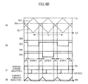
- Fig. 4A shows a step-up operation in a case where power to be stepped-up from the DC voltage V0 to the DC voltage V2 is large (high load) and this is a current-continuing operation with which an inductor current is always flowing.
- Fig. 4A shows a step-up operation in a case where power to be stepped-up from the DC voltage V0 to the DC voltage V2 is large (high load) and this is a current-continuing operation with which an inductor current is always flowing.
- FIG. 4B shows a step-up operation in a case where power to be stepped-up from the DC current V0 to the DC voltage V2 is small (low load) and this is a current-discontinuing operation with which there is a period during which no inductor current is flowing.
- Fig. 5A and Fig. 5B are waveform charts in the switching mode [2] showing an operation of the DC-DC power conversion apparatus 10 of the first embodiment to step-up the DC voltage V0 to the DC voltage V2 that is less than double the DC voltage V0 (a voltage ratio V2/V0 is smaller than 2 and a direction of power transmission is V0 ⁇ V2).
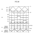
- Fig. 5A shows a step-up operation in a case where power to be stepped-up from the DC voltage V0 to the DC voltage V2 is large (high load) and this is a current-continuing operation with which an inductor current is always flowing.
- Fig. 5A shows a step-up operation in a case where power to be stepped-up from the DC voltage V0 to the DC voltage V2 is large (high load) and this is a current-continuing operation with which an inductor current is always flowing.
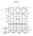
- 5B shows a step-up operation in a case where power to be stepped-up from the DC current V0 to the DC voltage V2 is small (low load) and this is a current-discontinuing operation with which there is a period during which no inductor current is flowing.
- Fig. 6A and Fig. 6B are waveform charts in the switching mode [3] showing an operation of the DC-DC power conversion apparatus 10 of the first embodiment to step-down the DC voltage V2 to the DC voltage V0 that is less than 1/2-time the DC voltage V2 (a voltage ratio V2/V0 is greater than 2 and a direction of power transmission is V2 ⁇ V0).
- Fig. 6A shows a step-down operation in a case where power to be stepped-down from the DC voltage V2 to the DC voltage V0 is large (high load) and this is a current-continuing operation with which an inductor current is always flowing.
- Fig. 6A shows a step-down operation in a case where power to be stepped-down from the DC voltage V2 to the DC voltage V0 is large (high load) and this is a current-continuing operation with which an inductor current is always flowing.
- 6B shows a step-down operation in a case where power to be stepped-down from the DC current V2 to the DC voltage V0 is small (low load) and this is a current-discontinuing operation with which there is a period during which no inductor current is flowing.
- Fig. 7A and Fig. 7B are waveform charts in the switching mode [4] showing an operation of the DC-DC power conversion apparatus 10 of the first embodiment to step-down the DC voltage V2 to the DC voltage V0 that is more than 1/2-time the DC voltage V2 (a voltage ratio V2/V0 is smaller than 2 and a direction of power transmission is V2 ⁇ V0).
- Fig. 7A shows a step-down operation in a case where power to be stepped-down from the DC voltage V2 to the DC voltage V0 is large (high load) and this is a current-continuing operation with which an inductor current is always flowing.
- Fig. 7A shows a step-down operation in a case where power to be stepped-down from the DC voltage V2 to the DC voltage V0 is large (high load) and this is a current-continuing operation with which an inductor current is always flowing.
- FIG. 7B shows a step-down operation in a case where power to be stepped-down from the DC current V2 to the DC voltage V0 is small (low load) and this is a current-discontinuing operation with which there is a period during which no inductor current is flowing.
- Fig. 4A , Fig. 4B , Fig. 5A , Fig. 5B , Fig. 6A , Fig. 6B , Fig. 7A , and Fig. 7B (a) shows chop signals Sc1 and Sc2 and a duty signal Sda(or 1-Sdb), (b) shows the gate signals G1a, G1b, G2a, and G2b, (c) shows a voltage across the inductor L, and (d) shows a current through the inductor L.
- the abscissa axes of Fig. 4A , Fig. 4B , Fig. 5A , Fig. 5B , Fig. 6A , Fig. 6B , Fig. 7A , and Fig. 7B are common time axes.
- FIG. 7B not only the gate signals G1a, G1b, G2a, and G2b but also zones 1 through 9 are shown along the time axis.
- FIG. 4A , Fig. 4B , Fig. 5A , Fig. 5B , Fig. 6A , Fig. 6B , Fig. 7A , and Fig. 7B a voltage across the inductor L is shown by a solid line.
- FIG. 4A , Fig. 4B , Fig. 5A , Fig. 5B , Fig. 6A , Fig. 6B , Fig. 7A , and Fig. 7B a current through the inductor L is shown by a solid line and also an average current Ildc is shown by a broken line.
- the chop signals Sc1 and Sc2 are compared with the duty signal Sda and the gate signals G1a and G2a are outputted. Also, the chop signals Sc1 and Sc2 are compared with the duty signal Sdb and the gate signals G1b and G2b are outputted. Cycles of the chop signals Sc1 and Sc2 are denoted by Ts and a phase of the chop signal Sc2 is delayed by 180° with respect to the chop signal Sc1. Also, the chop signals Sc1 and Sc2 are chop signals having amplitude of 1.0. Regarding the chop signals Sc1 and Sc2, magnitude of a signal level corresponding to a valley of chop signals is 0.0 and magnitude of a signal level corresponding to a peak of chop signals is 1.0.
- the gate signal G1a When the duty signal Sda is greater than the chop signal Sc1, the gate signal G1a is a high signal and when the duty signal Sda is smaller than the chop signal Sc1, the gate signal G1a is a low signal.
- the gate signal G2a When the duty signal Sda is greater than the chop signal Sc2, the gate signal G2a is a high signal and when the duty signal Sda is smaller than the chop signal Sc2, the gate signal G2a is a low signal.
- (1 - Sdb) as the duty signal Sdb is smaller than the chop signal Sc1 the gate signal G1b is a high signal, and when (1 - Sdb) is greater than the chop signal Sc1, the gate signal G1b is a low signal.
- the gate signal G2b When (1 - Sdb) is smaller than the chop signal Sc2, the gate signal G2b is a high signal, and when (1 - Sdb) is greater than the chop signal Sc2, the gate signal G2b is a low signal.
- ON times T1a, T1b, T2a, and T2b in one switching cycle of the semiconductor switching elements S1a, S1b, S2a, and S2b, respectively, are expressed by equations as follows.
- the zone 1 is a zone in which the gate signal G1a is a high signal, the gate signal G1b is a low signal, the gate signal G2a is a high signal, and the gate signal G2b is a low signal.
- the zone 2 is given as a zone in which G1a is a high signal, G1b is a low signal, G2a is a low signal, and G2b is a high signal.
- the zone 3 is given as a zone in which G1a is a low signal, G1b is a high signal, G2a is a high signal, and G2b is a low signal.
- the zone 4 is given as a zone in which G1a is a low signal, G1b is a high signal, G2a is a low signal, and G2b is a high signal.
- the zone 5 is given as a zone in which G1a is a high signal, G1b is a low signal, G2a is a low signal, and G2b is a low signal.
- the zone 6 is given as a zone in which G1a is a low signal, G1b is a low signal, G2a is a high signal, and G2b is a low signal.
- the zone 7 is given as a zone in which G1a is a low signal, G1b is a high signal, G2a is a low signal, and G2b is a low signal.
- the zone 8 is given as a zone in which G1a is a low signal, G1b is a low signal, G2a is a low signal, and G2b is a high signal.
- the zone 9 is given as a zone in which G1a is a low signal, G1b is a low signal, G2a is a low signal, and G2b is a low signal. The above is set forth in Table 1 below.
- Ts1, Ts5, and Ts6 of the zone 1, the zone 5, and the zone 6, respectively, in one switching cycle are expressed by equations below.
- Ts1 is a time per occurrence.
- Ts ⁇ 5 1 - Sda ⁇ Ts
- Ts ⁇ 6 1 - Sda ⁇ Ts
- a step-up operation in a case where power to be stepped-up from the DC voltage V0 to the DC voltage V2 is small (low load) will now be described below with reference to Fig. 4B .
- An operation in one cycle will be described in order of the zone 1, the zone 6, the zone 1, and the zone 5 in time sequence.
- a low load there is a period during which a current through the inductor L remains 0.
- the gate signals G1a and G2a are high signals and therefore the semiconductor switching elements S1a and S2a are ON, a voltage is applied to the inductor L and a current starts to flow in a path specified in the following.
- the DC voltage V0 is applied to the inductor L and the current increases from 0.
- a zone 51 is a zone in which a current is flowing through the inductor in the zone 5.
- Ts51 be a time of the zone 51, then Equation 11 below is obtained in the same manner.
- Ts ⁇ 51 V ⁇ 0 / V ⁇ 2 / 2 - V ⁇ 0 ⁇ Sda - 0.5 ⁇ Ts
- the inductor average current Ildc that is an average current in one cycle of the inductor is expressed by Equation 12 as follows.
- power P to be stepped-up from the DC voltage V0 to the stepped-up DC voltage V2 can be expressed by Equation 13 below.
- Ts9, Ts5, and Ts6 of the zone 9, the zone 5, and the zone 6, respectively, in one switching cycle are expressed as below.
- Ts9 is a time per occurrence.
- Ts ⁇ 5 Sda ⁇ Ts
- Ts ⁇ 6 Sda ⁇ Ts
- a step-up operation in a case where power to be stepped-up from the DC voltage V0 to the DC voltage V2 is small (low load) will now be described below with reference to Fig. 5B .
- An operation in one cycle will be described in order of the zone 5, the zone 9, the zone 6, and the zone 9 in time sequence.
- a low load there is a period during which a current through the inductor L remains 0.
- the gate signal G1a is a high signal and therefore the semiconductor switching element S1a is ON, a voltage is applied to the inductor L and a current starts to flow in a path specified in the following.
- a DC voltage (V0 - V2/2) is applied to the inductor L and the current increases from 0.
- an applied voltage to the inductor L is a negative voltage, (V0 - V2), and an inductor current decreases.
- V0 - V2 negative voltage
- the inductor average current Ildc that is an average current in one cycle of the inductor is expressed by Equation 20 as follows.
- power P to be stepped-up from the DC voltage V0 to the stepped-up DC voltage V2 can be expressed by Equation 21 below.
- an ON-duty (duty signal Sda) of the semiconductor switching elements S1a and S2a it becomes possible to adjust the power P.
- V ⁇ 0 ⁇ Ildc 0.5 ⁇ V ⁇ 0 ⁇ V ⁇ 2 ⁇ V ⁇ 0 - V ⁇ 2 / 2 / V ⁇ 2 - V ⁇ 0 ⁇ Sda 2 ⁇ Ts / L
- an ON-duty (duty signal Sda) of the semiconductor switching elements S1a and S2a it becomes possible to control the power P and hence to control a voltage ratio of the DC voltages V0 and V2.
- Ts8, Ts9, and Ts7 of the zone 8, the zone 9, and the zone 7, respectively, in one switching cycle are expressed as below.
- Ts9 is a time per occurrence.
- Ts ⁇ 8 Sdb ⁇ Ts
- Ts ⁇ 7 Sdb ⁇ Ts
- a step-down operation in a case where power to be stepped-down from the DC voltage V2 to the DC voltage V0 is small (low load) will now be described below with reference to Fig. 6B .
- An operation in one cycle will be described in order of the zone 8, the zone 9, the zone 7, and the zone 9 in time sequence.
- a low load there is a period during which a current through the inductor L remains 0.
- the gate signal G2b is a high signal and therefore the semiconductor switching element S2b is ON, a voltage is applied to the inductor L and a current starts to flow in a path specified in the following.
- a negative voltage (V0-V2/2) is applied to the inductor L and the current increases in a negative direction.
- an average current Ildc of the inductor L will be described.
- a voltage (V0 - V2/2) is applied to the inductor.
- power P to be stepped-down from the DC voltage V2 to the stepped-down DC voltage V0 can be expressed by Equation 29 below.
- an ON-duty (duty signal Sdb) of the semiconductor switching elements S1b and S2b it becomes possible to adjust the power P.
- the power P is stepped-down in a normal direction.
- Ts8, Ts7, and Ts4 of the zone 8, the zone 7, and the zone 4, respectively, in one switching cycle are expressed as below.
- Ts4 is a time per occurrence.
- Ts ⁇ 8 1 - Sdb ⁇ Ts
- Ts ⁇ 7 1 - Sdb ⁇ Ts
- a step-down operation in a case where power to be stepped-down from the DC voltage V2 to the DC voltage V0 is small (low load) will now be described below with reference to Fig. 7B .
- An operation in one cycle will be described in order of the zone 4, the zone 7, the zone 4, and the zone 8 in time sequence.
- a low load there is a period during which a current through the inductor L remains 0.
- the gate signals G1b and G2b are high signals and therefore the semiconductor switching elements S1b and S2b are ON, a voltage is applied to the inductor L and a current starts to flow in a path specified in the following.
- V0 - V2 negative voltage
- an applied voltage to the inductor L is a positive voltage, (V0 - V2/2), and an inductor current flowing in a negative direction decreases.
- the inductor current decreases, the current eventually becomes 0 at a midpoint in the zone 8 and the current remains 0 for the rest of the period in the zone 8.
- Ts71 and Ts81 are zones in which a current is flowing through the inductor in the zones 7 and 8, respectively.
- Ts71 and Ts81 be times of the zone 71 and the zone 81, respectively.
- V0 - V2/2 a voltage
- Ts71 and Ts81 are expressed by Equation 35 as follows.
- an inductor average current Ildc that is an average current in one cycle of the inductor is expressed by Equation 36 as follows.
- power P to be stepped-down from the DC voltage V2 to the stepped-down DC voltage V0 can be expressed by Equation 37 below.
- an ON-duty (duty signal Sdb) of the semiconductor switching elements S1b and S2b it becomes possible to adjust the power P.
- the power P is stepped-down in a normal direction.
- Fig. 8A shows a step-up operation in a case where power to be stepped-up from the DC voltage V0 to the DC voltage V2 is large (high load) and Fig. 8B shows a step-up operation in a case where power to be stepped-up from the DC voltage V0 to the DC voltage V2 is small (low load).
- the semiconductor switching elements S1a and S1b perform switching operations complementarily and the semiconductor switching elements S2a and S2b perform switching operations complementarily.
- Fig. 8A and Fig. 8B one cycle is made up of the zone 1, the zone 2, and the zone 3 and no other zones are present.
- the voltage V0 is applied to the inductor and a voltage (V0 - V2/2) is applied to the inductor in the zone 2 and the zone 3.
- V0 - V2/2 a voltage
- a current flowing through the inductor L is the same in the DC-DC power conversion apparatus of the first embodiment and the example of the related art. It should be appreciated, however, that, as is shown in Fig. 8B , a certain ripple current flows through the inductor L even in an operation under low load in the apparatus in the related art.
- Fig. 9 shows power conversion efficiency (broken line A) of the DC-DC power conversion apparatus of the first embodiment and power conversion efficiency (solid line B) of the example in the related art in an operation to step-up the DC voltage V0 to the DC voltage V2 that is more than double the DC voltage V0 (a voltage ratio V2/V0 is greater than 2 and a direction of power transmission is V0 ⁇ V2).
- power conversion efficiency of the DC-DC power conversion apparatus of the first embodiment is enhanced when power to be stepped-up is small owing to a current-discontinuing operation with which a current through the inductor becomes 0 in a part of periods. The same applies to the other switching modes.
- the DC-DC power conversion apparatus has two or more switching units each of which includes two semiconductor switching elements Sa and Sb performing switching operations, which semiconductor switching elements of the respective switching units are all connected in series, an energy transition capacitor for conducting charging/discharging according to the switching operations of the respective semiconductor switching elements of the respective switching units, and an inductor.
- the DC-DC power conversion apparatus is provided with a control unit that makes the semiconductor switching elements of the switching units execute switching operations in four types of switching modes, according to a ratio of input/output voltages of the DC-DC power conversion apparatus and a direction of power transmission in the DC-DC power conversion apparatus, and also makes the semiconductor switching elements carry out a current-discontinuing operation wherein a current flowing through the inductor becomes 0 during the switching operations under low load.
- switching modes [1] through [4] it becomes possible to readily control a voltage ratio of the DC voltages V0 and V2.
- switching modes [1] through [4] are as follows .
- V0 be one DC voltage of the DC-DC power conversion apparatus and V2 be the other DC voltage.
- IGBTs and diodes are used as the semiconductor switching elements. It should be appreciated, however, that other semiconductor switching elements formed of MOSFETs and diodes may be used instead. In the case of MOSFETs, synchronous rectification can be achieved by switching ON the MOSFET while a current is flowing through the diode. Hence, it becomes possible to increase power conversion efficiency further.
- Si semiconductors are often used for the semiconductor switching elements. It should be appreciated, however, that wide-gap semiconductors, such as SiC and GaN, can be used as well. By using wide-gap semiconductors, such as SiC and GaN, it becomes possible to lessen a conduction loss and a switching loss in the semiconductor switching elements. Hence, it becomes possible to achieve a DC-DC power conversion apparatus with further higher power conversion efficiency.
- FIG. 10 is a circuit diagram showing a configuration of a main circuit of a DC-DC power conversion apparatus according to a second embodiment of the invention.
- a DC-DC power conversion apparatus 40 of the second embodiment is a two-way DC-DC power conversion apparatus furnished with a step-up function of converting a DC voltage V0 inputted between a voltage terminal VL and a voltage terminal VN to a stepped-up DC voltage V2 and outputting the DC voltage V2 between a voltage terminal VH and a voltage terminal VN2, and a step-down function of converting the DC voltage V2 inputted between the voltage terminal VH and the voltage terminal VN2 to the stepped-down DC voltage V0 and outputting the DC voltage V0 between the voltage terminal VL and the voltage terminal VN.
- the DC-DC power conversion apparatus 40 of the second embodiment is different from the DC-DC power conversion apparatus 10 of the first embodiment above shown in Fig. 1 in a connection configuration of the main circuit.
- connections of the main circuit of the DC-DC power conversion apparatus 40 of the second embodiment will be described in detail.
- an emitter terminal of an IGBT forming a semiconductor switching element S1a is connected to a voltage terminal VN and a collector terminal thereof is connected to a high-voltage end terminal of a smoothing capacitor (energy transition capacitor) C10.
- An emitter terminal of an IGBT forming a semiconductor switching element S1b is connected to a low-voltage end terminal VN2 of the smoothing capacitor (energy transition capacitor) C10 and a collector terminal thereof is connected to the voltage terminal VN.
- An emitter terminal of an IGBT forming a semiconductor switching element S2b is connected to a voltage terminal VM and a collector terminal thereof is connected to a high-voltage end terminal VH of a smoothing capacitor (energy transition capacitor) C11.
- An emitter terminal of an IGBT forming a semiconductor switching element S2a is connected to a high-voltage terminal of the smoothing capacitor (energy transition capacitor) C10 and a low-voltage end terminal of the smoothing capacitor (energy transition capacitor) C11, and a collector terminal thereof is connected to the voltage terminal VM.
- the semiconductor switching elements S1a and S1b perform switching operations and form a switching unit SU1. Also, the semiconductor switching elements S2a and S2b perform switching operations as well and form a switching unit SU2.
- the low-voltage end terminal of the smoothing capacitor C0 is connected to the voltage terminal VN and the high-voltage end terminal of the smoothing capacitor C0 is connected to the voltage terminal VL.
- the low-voltage end terminal of the smoothing capacitor C2 is connected to the low-voltage end terminal of the smoothing capacitor (energy transition capacitor) C10 and the high-voltage end terminal of the smoothing capacitor C2 is connected to the high-voltage end terminal of the smoothing capacitor (energy transition capacitor) C11.
- the high-voltage end terminal of the smoothing capacitor (energy transition capacitor) C10 and the low-voltage end terminal of the smoothing capacitor (energy transition capacitor) C11 are connected to each other.
- One terminal of the inductor L is connected to the voltage terminal VL and the other terminal thereof is connected to the voltage terminal VM.
- the smoothing capacitor C2 is used.
- a series body of the smoothing capacitors (energy transition capacitors) C10 and C11 is connected to the smoothing capacitor C2 in parallel, the smoothing capacitor C2 may be eliminated.
- the smoothing capacitor C10 and the smoothing capacitor C11 divide a voltage V2 between the voltage terminals VH and VN2 into two halves. Hence, V2/2 is given as a voltage across each of the capacitors C10 and C11.
- a gate terminal of the semiconductor switching element S1b is connected to an output terminal of a gate drive circuit 101b and a gate signal G1b is inputted into an input terminal of the gate drive circuit 101b.
- a gate terminal of the semiconductor switching element S1a is connected to an output terminal of a gate drive circuit 101a and a gate signal G1a is inputted into an input terminal of the gate drive circuit 101a.
- a gate terminal of the semiconductor switching element S2b is connected to an output terminal of a gate drive circuit 102b and a gate signal G2b is inputted into an input terminal of the gate drive circuit 102b.
- a gate terminal of the semiconductor switching element S2a is connected to an output terminal of a gate drive circuit 102a and a gate signal G2a is inputted into an input terminal of the gate drive circuit 102a.
- a control unit of the DC-DC power conversion apparatus 40 of the second embodiment is the same as the control unit of the DC-DC power conversion apparatus 10 of the first embodiment above in configuration and operation.
- a voltage across the inductor L is the same as that in the DC-DC power conversion apparatus of the first embodiment above and a current flowing through the inductor L is also the same. Accordingly, the DC-DC power conversion apparatus of the second embodiment can also obtain the advantage same as that obtained by the DC-DC power conversion apparatus of the first embodiment above.
- the invention is effectively used for a DC-DC power conversion apparatus that converts a DC voltage to a stepped-up or stepped-down DC voltage.
Landscapes
- Engineering & Computer Science (AREA)
- Power Engineering (AREA)
- Dc-Dc Converters (AREA)
Abstract
Description
- The present invention relates to a DC-DC power conversion apparatus that converts a DC voltage to a stepped-up or stepped-down DC voltage.
- There is a DC-DC power conversion apparatus in the related art having two or more switching units each of which includes two or more semiconductor switching elements that perform switching operations complementarily. All the semiconductor switching elements of the respective switching units are connected in series. The DC-DC power conversion apparatus also has an energy transition capacitor and an inductor. DC-DC conversion is performed using charging/discharging of the energy transition capacitor by switching operations of the semiconductor switching elements of the respective switching units. Low-voltage withstanding semiconductor switching elements and a small inductor can be used and a ratio of an input voltage and an output voltage can be adjusted by changing ON-duties of the semiconductor switching elements (for example, see Patent Document 1).
-
- Patent Document 1: Japanese Patent No.
3414749 -
- Non-Patent Document 1: Thierry A. Meynard et al: "Multicell Converters: Basic Concepts and Industry Applications", IEEE TRANSACTIONS ON INDUSTRIAL ELECTRONICS, VOL. 49, NO. 5, OCTOBER 2002
- The DC-DC power conversion apparatus in the related art uses the energy transition capacitor and the inductor to perform DC-DC power conversion using charging/discharging of the energy transition capacitor, and low-voltage withstanding semiconductor switching elements and a small inductor can be used.
In the DC-DC power conversion apparatus in the related art, however, two semiconductor switching elements perform switching operations complementarily. Accordingly, a certain ripple current flows through the inductor independently of an amount of load, and a loss occurs because this current flows further through the energy transition capacitor and the semiconductor switching elements. Hence, power conversion efficiency is low under low load.
Meanwhile, when an inductance value of the inductor is increased, a ripple current decreases and therefore a loss can be lessened. Hence, it becomes possible to increase power conversion efficiency under low load. However, when an inductance value is increased, there arises a problem that a volume and a weight of the inductor are increased and so are a volume and a weight of the DC-DC power conversion apparatus. - The invention is devised to solve the problem as above and has an object to provide an improved DC-DC power conversion apparatus capable of reducing a loss under low load even when a small and light inductor having a small inductance value is used.
- A DC-DC power conversion apparatus of the invention has two or more switching units each of which includes two semiconductor switching elements Sa and Sb performing switching operations, which semiconductor switching elements of the respective switching units are all connected in series, an energy transition capacitor for conducting charging/discharging according to the switching operations of the respective semiconductor switching elements of the respective switching units, and an inductor. The DC-DC power conversion apparatus is provided with a control unit that makes the semiconductor switching elements of the switching units execute switching operations in four types of switching modes, according to a ratio of input/output voltages of the DC-DC power conversion apparatus and a direction of power transmission in the DC-DC power conversion apparatus, and also makes the semiconductor switching elements carry out a current-discontinuing operation wherein a current flowing through the inductor becomes 0 during the switching operations under low load.
- According to the DC-DC power conversion apparatus of the invention, because the DC-DC power conversion apparatus has means for performing operations in four types of switching modes according to a ratio of input/output voltages of the DC-DC power conversion apparatus and a direction of power transmission in the DC-DC power conversion apparatus, the semiconductor switching elements perform a current-discontinuing operation with which an inductor current becomes 0 under low load. Hence, even when a small inductor having a small inductance value is used, a ripple current through the inductor under low load decreases and losses in the energy transition capacitor, the inductor, and the semiconductor switching elements can be lessened. It thus becomes possible to increase power conversion efficiency under low load.
- The foregoing and other objects features, aspects, and advantages of the present invention will become more apparent from the following detailed description of the present invention when taken conjunction with the accompanying drawings.
-
-
Fig. 1 is an electrical circuit diagram showing a configuration of a main circuit of a DC-DC power conversion apparatus according to a first embodiment of the invention. -
Fig. 2 is a view of an overall configuration showing a connection relation among a power supply, a motor generator, and the DC-DC power conversion apparatus according to the first embodiment of the invention. -
Fig. 3 is a block diagram showing a configuration of a control unit of the DC-DC power conversion apparatus according to the first embodiment of the invention. -
Fig. 4A is a waveform chart showing an operation of the DC-DC power conversion apparatus according to the first embodiment of the invention, that is, a waveform chart of a step-up operation under high load when a voltage ratio is 2 or greater. -
Fig. 4B is a waveform chart showing an operation of the DC-DC power conversion apparatus according to the first embodiment of the invention, that is, a waveform chart of a step-up operation under low load when a voltage ratio is 2 or greater. -
Fig. 5A is a waveform chart showing an operation of the DC-DC power conversion apparatus according to the first embodiment of the invention, that is, a waveform chart of a step-up operation under high load when a voltage ratio is 2 or smaller. -
Fig. 5B is a waveform chart showing an operation of the DC-DC power conversion apparatus according to the first embodiment of the invention, that is, a waveform chart of a step-up operation under low load when a voltage ratio is 2 or smaller. -
Fig. 6A is a waveform chart showing an operation of the DC-DC power conversion apparatus according to the first embodiment of the invention, that is, a waveform chart of a step-down operation under high load when a voltage ratio is 2 or greater. -
Fig. 6B is a waveform chart showing an operation of the DC-DC power conversion apparatus according to the first embodiment of the invention, that is, a waveform chart of a step-down operation under low load when a voltage ratio is 2 or greater. -
Fig. 7A is a waveform chart showing an operation of the DC-DC power conversion apparatus according to the first embodiment of the invention, that is, a waveform chart of a step-down operation under high load when a voltage ratio is 2 or smaller. -
Fig. 7B is a waveform chart showing an operation of the DC-DC power conversion apparatus according to the first embodiment of the invention, that is, a waveform chart of a step-down operation under low load when a voltage ratio is 2 or smaller. -
Fig. 8A is a waveform chart showing a step-up operation under high load of a DC-DC power conversion apparatus in the related art. -
Fig. 8B is a waveform chart showing a step-up operation under low load of a DC-DC power conversion apparatus in the related art. -
Fig. 9 is a view showing power conversion efficiency of the DC-DC power conversion apparatus according to the first embodiment of the invention. -
Fig. 10 is an electrical circuit diagram showing a configuration of a main circuit of a DC-DC power conversion apparatus according to a second embodiment of the invention. - Hereinafter, embodiments of the invention will be described with reference to the drawings. In the respective drawings, same reference numerals denote same or equivalent portions.
-
Fig. 1 is an electrical circuit diagram showing a configuration of a main circuit of a DC-DCpower conversion apparatus 10 according to a first embodiment of the invention.
The DC-DCpower conversion apparatus 10 of the first embodiment is a two-way DC-DC power conversion apparatus furnished with a step-up function of converting a DC voltage V0 inputted between a voltage terminal VL and a voltage terminal VN to a stepped-up DC voltage V2 and outputting the DC voltage V2 between a voltage terminal VH and the voltage terminal VN, and a step-down function of converting the DC voltage V2 inputted between the voltage terminal VH and the voltage terminal VN to the stepped-down DC voltage V0 and outputting the DC voltage V0 between the voltage terminal VL and the voltage terminal VN. - Referring to
Fig. 1 , the main circuit of the DC-DCpower conversion apparatus 10 includes smoothing capacitors C0 and C2 that smooth input/output DC voltages V0 and V2, respectively, a smoothing capacitor C1 functioning as an energy transition capacitor, a plurality of semiconductor switching elements S1a, S1b, S2a, and S2b, and an inductor L. The semiconductor switching elements S1a and S1b form a switching unit SU1 and the semiconductor switching elements S2a and S2b form a switching unit SU2. - Each of the semiconductor switching elements S1a, S1b, S2a, and S2b is formed of an IGBT (Insulated Gate Bipolar Transistor) and a diode connected to the IGBT in antiparallel.
The IGBT of each of the semiconductor switching elements S1a, S1b, S2a, and S2b has a collector terminal, an emitter terminal, and a gate terminal. The diode of each of the semiconductor switching elements S1a, S1b, S2a, and S2b is connected between the collector terminal and the emitter terminal of the IGBT of the corresponding semiconductor switching element S1a, S1b, S2a, or S2b in antiparallel so that an anode terminal is connected to the emitter terminal. - Connections of the DC-DC
power conversion apparatus 10 will be described in detail.
The emitter terminal of the IGBT of the semiconductor switching element S1b is connected to a voltage terminal VM and the collector terminal thereof is connected to a high-voltage end terminal of the smoothing capacitor (energy transition capacitor) C1. The emitter terminal of the IGBT of the semiconductors switching element S1a is connected to a low-voltage end terminal of the smoothing capacitor (energy transition capacitor) C1 and the collector terminal thereof is connected to the voltage terminal VM. The emitter terminal of the IGBT of the semiconductor switching element S2b is connected to a high-voltage end terminal of the smoothing capacitor (energy transition capacitor) C1 and the collector terminal thereof is connected to a high-voltage end terminal of the smoothing capacitor C2. The emitter terminal of the IGBT of the semiconductor switching element S2a is connected to a low-voltage end terminal of the smoothing capacitor C2 and the collector terminal thereof is connected to the low-voltage end terminal of the smoothing capacitor (energy transition capacitor) C1, - A low-voltage end terminal of the smoothing capacitor C0 is connected to the voltage terminal VN and a high-voltage end terminal of the smoothing capacitor C0 is connected to the voltage terminal VL. The low-voltage end terminal of the smoothing capacitor C2 is connected to the voltage terminal VN and the high-voltage end terminal of the smoothing capacitor C2 is connected to the voltage terminal VH. One end of the inductor L is connected to the voltage terminal VL and the other end is connected to the voltage terminal VM.
- The gate terminal of the IGBT of the semiconductor switching element S1b is connected to an output terminal of a
gate drive circuit 101b and a gate signal G1b is inputted into an input terminal of thegate drive circuit 101b. The gate terminal of the IGBT of the semiconductor switching element S1a is connected to an output terminal of agate drive circuit 101a and a gate signal G1a is inputted into an input terminal of thegate drive circuit 101a. The gate terminal of the IGBT of the semiconductor switching element S2b is connected to an output terminal of agate drive circuit 102b and a gate signal G2b is inputted into an input terminal of thegate drive circuit 102b. The gate terminal of the IGBT of the semiconductor switching element S2a is connected to an output terminal of agate drive circuit 102a and a gate signal G2a is inputted into an input terminal of thegate drive circuit 102a. -
Fig. 2 is a view of an overall configuration showing connections among the DC-DCpower conversion apparatus 10, a power supply, and a motor generator. A battery Vs functioning as a voltage source is connected between the voltage terminals VL and VN of the DC-DCpower conversion apparatus 10 and a DC terminal of a three-phase inverter INV is connected between the voltage terminals VH and VN. A motor generator MG is connected to AC terminals of the three-phase inverter INV.
When the motor generator MG performs a power running operation, the DC-DCpower conversion apparatus 10 performs a step-up operation to output a DC voltage V0 inputted between the voltage terminals VL and VN as a stepped-up DC voltage V2. When the motor generator MG performs a regenerative operation, the DC-DCpower conversion apparatus 10 performs a step-down operation to output a DC voltage V2 inputted between the voltage terminals VH and VN as a stepped-down DC voltage V0. -
Fig. 3 is a block diagram showing a configuration of a control unit of the DC-DCpower conversion apparatus 10.
The control unit includes a switchingmode output portion 310, a PWMwaveform output portion 320, a step-up/downdiscrimination portion 330, and acomputation portion 340.
Thecomputation portion 340 receives inputs of a voltage command value V2* of the DC voltage V2 and the DC voltage V2 and outputs an inductor average current command value ILdc*. The step-up/downdiscrimination portion 330 receives an input of the inductor average current command value ILdc* and outputs a step-up/down signal UD. The switchingmode output portion 310 receives inputs of the step-up/down signal UD and the DC voltages V0 and V2 and outputs a switching mode signal SM. The PWMwaveform output portion 320 receives inputs of the switching mode signal SM and the inductor average current command value ILdc* and outputs gate signals G1a, G1b, G2a, and G2b.
The gate signals G1a, G1b, G2a, and G2b are connected to the respective semiconductor switching elements via the corresponding gate drive circuits. The semiconductor switching elements S1a, S1b, S2a, and S2b switch ON when the gate signals G1a, G1b, G2a, and G2b, respectively, are high signals and switch OFF when the gate signals G1a, G1b, G2a, and G2b, respectively, are low signals. - The
computation portion 340 calculates a difference between the voltage commend value V2* and the voltage V2 to perform a proportional-integral operation and outputs the result as the inductor average current command value ILdc*. Feedback control on the DC voltage V2 is performed by outputting the inductor average current command value ILdc* so that the DC voltage V2 follows the current command value V2*.
The step-up/downdiscrimination portion 330 determines that the ongoing operation is a step-up operation when the inductor average current command value ILdc* is positive and outputs: step-up/down signal UD = step-up signal. When the inductor average current command value ILdc* is negative, the step-up/downdiscrimination portion 330 determines that the ongoing operation is a step-down operation and outputs: step-up/down signal UD = step-down signal. - The switching
mode selection portion 310 selects a switching mode and outputs the switching mode signal SM.
In a case where the ongoing operation is a step-up operation and a voltage ratio V2/V0 is greater than 2, the switchingmode output portion 310 selects a switching mode [1] and outputs: switching mode signal SM = switching mode [1]. In a case where the ongoing operation is a step-up operation and a voltage ratio V2/V0 is smaller than 2, the switchingmode output portion 310 selects a switching mode [2] and outputs: switching mode signal SM = switching mode [2].
In a case where the ongoing operation is a step-down operation and a voltage ratio V2/V0 is greater than 2, the switchingmode output portion 310 selects a switching mode [3] and outputs: switching mode signal SM = switching mode [3] In a case where the ongoing operation is a step-down operation and a voltage ratio V2/V0 is smaller than 2, the switchingmode output portion 310 selects a switching mode [4] and outputs: switching mode signal SM = switching mode [4]. It should be noted that a voltage ratio V2/V0 is 1 or greater independently of operation modes. - The PWM
waveform output portion 320 outputs the gate signals G1a, G1b, G2a, and G2b on the basis of the switching mode and a value of the inductor average current command value ILdc*.
In the case of the switching mode [1], the PWMwaveform output portion 320 outputs the gate signals G1a, G1b, G2a, and G2b with which an ON-duty of the semiconductor switching elements S1a and S2a is 50% or higher and an ON-duty of the semiconductor switching elements S1b and S2b is 0%.
In the case of the switching mode [2], the PWMwaveform output portion 320 outputs the gate signals G1a, G1b, G2a, and G2b with which an ON-duty of the semiconductor switching elements Sa1 and Sa2 is 50% or below and an ON-duty of the semiconductor switching elements S1b and S2b is 0%.
In the case of the switching mode [3], the PWMwaveform output portion 320 outputs the gate signals G1a, G1b, G2a, and G2b with which an ON-duty of the semiconductor switching elements S1a and S2a is 0% and an ON-duty of the semiconductor switching elements S1b and S2b is 50% or below.
In the case of the switching mode [4], the PWMwaveform output portion 320 outputs the gate signals G1a, G1b, G2a, and G2b with which an ON-duty of the semiconductor switching elements S1a and S2a is 0% and an ON-duty of the semiconductor switching elements S1b and S2b is 50% or higher. - An operation to convert a DC voltage to a stepped-up or stepped-down DC voltage will now be described.
In a steady state, an average voltage of a voltage Vc1 across the smoothing capacitor (energy transition capacitor) C1 is 1/2 the DC voltage V2, that is V2/2. Because the DC voltage V2 is charged to the smoothing capacitor C2, applied voltages to the respective semiconductor switching elements S1a, S1b, S2a, and S2b are substantially V2/2. Also, as is described inNon-Patent Document 1, a ripple voltage applied to the inductor L decreases and a frequency of the ripple voltage applied to the inductor L is double the switching frequency. Hence, a small inductor L can be used.
In addition, the gate signals G2a and G2b are signals phase-delayed by 180° with respect to the gate signals G1a and G1b. -
Fig. 4A andFig. 4B are waveform charts in the switching mode [1] showing an operation of the DC-DCpower conversion apparatus 10 of the first embodiment to step-up the DC voltage V0 to the DC voltage V2 that is more than double the DC voltage V0 (a voltage ratio V2/V0 is greater than 2 and a direction of power transmission is V0 → V2).
Fig. 4A shows a step-up operation in a case where power to be stepped-up from the DC voltage V0 to the DC voltage V2 is large (high load) and this is a current-continuing operation with which an inductor current is always flowing.
Fig. 4B shows a step-up operation in a case where power to be stepped-up from the DC current V0 to the DC voltage V2 is small (low load) and this is a current-discontinuing operation with which there is a period during which no inductor current is flowing. -
Fig. 5A andFig. 5B are waveform charts in the switching mode [2] showing an operation of the DC-DCpower conversion apparatus 10 of the first embodiment to step-up the DC voltage V0 to the DC voltage V2 that is less than double the DC voltage V0 (a voltage ratio V2/V0 is smaller than 2 and a direction of power transmission is V0 → V2).
Fig. 5A shows a step-up operation in a case where power to be stepped-up from the DC voltage V0 to the DC voltage V2 is large (high load) and this is a current-continuing operation with which an inductor current is always flowing.
Fig. 5B shows a step-up operation in a case where power to be stepped-up from the DC current V0 to the DC voltage V2 is small (low load) and this is a current-discontinuing operation with which there is a period during which no inductor current is flowing. -
Fig. 6A andFig. 6B are waveform charts in the switching mode [3] showing an operation of the DC-DCpower conversion apparatus 10 of the first embodiment to step-down the DC voltage V2 to the DC voltage V0 that is less than 1/2-time the DC voltage V2 (a voltage ratio V2/V0 is greater than 2 and a direction of power transmission is V2 → V0).
Fig. 6A shows a step-down operation in a case where power to be stepped-down from the DC voltage V2 to the DC voltage V0 is large (high load) and this is a current-continuing operation with which an inductor current is always flowing.
Fig. 6B shows a step-down operation in a case where power to be stepped-down from the DC current V2 to the DC voltage V0 is small (low load) and this is a current-discontinuing operation with which there is a period during which no inductor current is flowing. -
Fig. 7A andFig. 7B are waveform charts in the switching mode [4] showing an operation of the DC-DCpower conversion apparatus 10 of the first embodiment to step-down the DC voltage V2 to the DC voltage V0 that is more than 1/2-time the DC voltage V2 (a voltage ratio V2/V0 is smaller than 2 and a direction of power transmission is V2 → V0).
Fig. 7A shows a step-down operation in a case where power to be stepped-down from the DC voltage V2 to the DC voltage V0 is large (high load) and this is a current-continuing operation with which an inductor current is always flowing.
Fig. 7B shows a step-down operation in a case where power to be stepped-down from the DC current V2 to the DC voltage V0 is small (low load) and this is a current-discontinuing operation with which there is a period during which no inductor current is flowing. - In
Fig. 4A ,Fig. 4B ,Fig. 5A ,Fig. 5B ,Fig. 6A ,Fig. 6B ,Fig. 7A , andFig. 7B, (a) shows chop signals Sc1 and Sc2 and a duty signal Sda(or 1-Sdb), (b) shows the gate signals G1a, G1b, G2a, and G2b, (c) shows a voltage across the inductor L, and (d) shows a current through the inductor L. It should be noted that the abscissa axes ofFig. 4A ,Fig. 4B ,Fig. 5A ,Fig. 5B ,Fig. 6A ,Fig. 6B ,Fig. 7A , andFig. 7B are common time axes. - In (a) of
Fig. 4A ,Fig. 4B ,Fig. 5A ,Fig. 5B ,Fig. 6A, Fig. 6B ,Fig. 7A , andFig. 7B , not only the chop signals Sc1 and Sc2 but also one switching cycle Ts is shown along the time axis. This is shown, by way of example, between two adjacent points at which the chop signal Sc1 drops to 0.0.
In (b) ofFig. 4A ,Fig. 4B ,Fig. 5A ,Fig. 5B ,Fig. 6A ,Fig. 6B ,Fig. 7A , andFig. 7B , not only the gate signals G1a, G1b, G2a, and G2b but alsozones 1 through 9 are shown along the time axis.
In (c) ofFig. 4A ,Fig. 4B ,Fig. 5A ,Fig. 5B ,Fig. 6A ,Fig. 6B ,Fig. 7A , andFig. 7B , a voltage across the inductor L is shown by a solid line.
In (d) ofFig. 4A ,Fig. 4B ,Fig. 5A ,Fig. 5B ,Fig. 6A ,Fig. 6B ,Fig. 7A , andFig. 7B , a current through the inductor L is shown by a solid line and also an average current Ildc is shown by a broken line. - Within the PWM
waveform output portion 320, the chop signals Sc1 and Sc2 are compared with the duty signal Sda and the gate signals G1a and G2a are outputted. Also, the chop signals Sc1 and Sc2 are compared with the duty signal Sdb and the gate signals G1b and G2b are outputted.
Cycles of the chop signals Sc1 and Sc2 are denoted by Ts and a phase of the chop signal Sc2 is delayed by 180° with respect to the chop signal Sc1. Also, the chop signals Sc1 and Sc2 are chop signals having amplitude of 1.0. Regarding the chop signals Sc1 and Sc2, magnitude of a signal level corresponding to a valley of chop signals is 0.0 and magnitude of a signal level corresponding to a peak of chop signals is 1.0. - When the duty signal Sda is greater than the chop signal Sc1, the gate signal G1a is a high signal and when the duty signal Sda is smaller than the chop signal Sc1, the gate signal G1a is a low signal. When the duty signal Sda is greater than the chop signal Sc2, the gate signal G2a is a high signal and when the duty signal Sda is smaller than the chop signal Sc2, the gate signal G2a is a low signal.
Also, when (1 - Sdb) as the duty signal Sdb is smaller than the chop signal Sc1, the gate signal G1b is a high signal, and when (1 - Sdb) is greater than the chop signal Sc1, the gate signal G1b is a low signal. When (1 - Sdb) is smaller than the chop signal Sc2, the gate signal G2b is a high signal, and when (1 - Sdb) is greater than the chop signal Sc2, the gate signal G2b is a low signal. - Also, ON times T1a, T1b, T2a, and T2b in one switching cycle of the semiconductor switching elements S1a, S1b, S2a, and S2b, respectively, are expressed by equations as follows.




- A description will be given on the assumption that the
zone 1 is a zone in which the gate signal G1a is a high signal, the gate signal G1b is a low signal, the gate signal G2a is a high signal, and the gate signal G2b is a low signal.
Also, thezone 2 is given as a zone in which G1a is a high signal, G1b is a low signal, G2a is a low signal, and G2b is a high signal.
Thezone 3 is given as a zone in which G1a is a low signal, G1b is a high signal, G2a is a high signal, and G2b is a low signal.
Thezone 4 is given as a zone in which G1a is a low signal, G1b is a high signal, G2a is a low signal, and G2b is a high signal.
Thezone 5 is given as a zone in which G1a is a high signal, G1b is a low signal, G2a is a low signal, and G2b is a low signal.
Thezone 6 is given as a zone in which G1a is a low signal, G1b is a low signal, G2a is a high signal, and G2b is a low signal.
Thezone 7 is given as a zone in which G1a is a low signal, G1b is a high signal, G2a is a low signal, and G2b is a low signal.
Thezone 8 is given as a zone in which G1a is a low signal, G1b is a low signal, G2a is a low signal, and G2b is a high signal. Thezone 9 is given as a zone in which G1a is a low signal, G1b is a low signal, G2a is a low signal, and G2b is a low signal.
The above is set forth in Table 1 below. -
[Table 1] Zone 1Zone 2Zone 3Zone 4Zone 5Zone 6Zone 7Zone 8Zone 9G2b Lo Hi Lo Hi Lo Lo Lo Hi Lo G2a Hi Lo Hi Lo Lo Hi Lo Lo Lo G1b Lo Lo Hi Hi Lo Lo Hi Lo Lo G1a Hi Hi Lo Lo Hi Lo Lo Lo Lo Lo: low signal
Hi: high signal - Operations in the respective switching modes will now be described.
An operation to step-up the DC voltage V0 to the DC voltage V2 that is more than double the DC voltage V0 (a voltage ratio V2/V0 is greater than 2 and a direction of power transmission is V0 → V2) in the switching mode [1] will be described usingFig. 4A andFig. 4B . As are shown inFig. 4A andFig. 4B , in the switching mode [1], an ON-duty of the semiconductor switching elements S1a and S2a is higher than 50% (Sda > 50%) and an ON-duty of the semiconductor switching elements S1b and S2b is 0% (Sdb = 0%). Hence, one cycle is made up of thezone 1, thezone 5, and thezone 6 and no other zones are present. - Also, times Ts1, Ts5, and Ts6 of the
zone 1, thezone 5, and thezone 6, respectively, in one switching cycle are expressed by equations below. For thezone 1 occurring twice in one cycle, Ts1 is a time per occurrence.


- Firstly, a step-up operation in a case where power to be stepped-up from the DC voltage V0 to the DC voltage V2 is large (high load) will be described below with reference to
Fig. 4A .
In the case of a high load, a current in a normal direction is always flowing through the inductor.
In thezone 1, because the gate signals G1a and G2a are high signals and therefore the semiconductor switching elements S1a and S2a are ON, a current flows in a path specified below and the voltage V0 is applied to the inductor L. For ease of description, a voltage drop across the semiconductor switching elements and the capacitors is 0.
Capacitor C0 → inductor L → IGBT of semiconductor switching element S1a → IGBT of semiconductor switching element S2a - In the
zone 6, because the semiconductor switching element S2a is ON, a current flows in a path specified below and a voltage (V0 - V2/2) is applied to the inductor L.
Capacitor C0 → Inductor L → diode of semiconductor switching element S1b → capacitor C1 → IGBT of semiconductor switching element S2a
In thezone 5, because the semiconductor switching element S1a is ON, a current flows in a path specified below and a voltage (V0 - V2/2) is applied to the inductor L.
Capacitor C0 → inductor L → IGBT of semiconductor switching element S1a → capacitor C1 → diode of semiconductor switching element S2b → capacitor C2 - A relation between the duty signal Sda and the input/output DC voltages V0 and V2 will also be described.
In a steady state, an average voltage across the inductor L in one switching cycle is 0 by neglecting a voltage drop caused by a resistance component and expressed as below, which is rewritten asEquation 8 below.

As is obvious fromEquation 8 above, by controlling the duty signal Sda under high load, it becomes possible to control a voltage ratio of the input/output DC voltages V0 and V2. - A step-up operation in a case where power to be stepped-up from the DC voltage V0 to the DC voltage V2 is small (low load) will now be described below with reference to
Fig. 4B .
An operation in one cycle will be described in order of thezone 1, thezone 6, thezone 1, and thezone 5 in time sequence. In the case of a low load, there is a period during which a current through the inductor L remains 0.
In thezone 1, because the gate signals G1a and G2a are high signals and therefore the semiconductor switching elements S1a and S2a are ON, a voltage is applied to the inductor L and a current starts to flow in a path specified in the following.
Capacitor C0 → inductor L → IGBT of semiconductor switching element S1a → IGBT of semiconductor switching element S2a
The DC voltage V0 is applied to the inductor L and the current increases from 0. - In the
zone 6, because the semiconductor switching element S2a is ON, a current flows in a path specified below at the beginning.
Capacitor C0 → inductor L → diode of semiconductor switching element S1b → capacitor C1 → IGBT of semiconductor switching element S2a
In this instance, an applied voltage to the inductor L is a negative voltage, (V0 - V2/2), and therefore an inductor current decreases. As the inductor current decreases, the current eventually becomes 0 at a midpoint in thezone 6 and the current remains 0 for the rest of the period in thezone 6.
In thezone 1, the current flows in the same manner as described above. - In the
zone 5, because the semiconductor switching element S1a is ON, a current flows in a path specified below at the beginning.
Capacitor C0 → inductor L → IGBT of semiconductor switching element S1a → capacitor C1 → diode of semiconductor switching element S2b → capacitor C2
In this instance, an applied voltage to the inductor L is a negative voltage, (V0 - V2/2), and therefore an inductor current decreases. As the inductor current decreases, the current eventually becomes 0 at a midpoint in thezone 5 and the current remains 0 for the rest of the period in thezone 5. - In this manner, a current-discontinuing operation with which a current through the inductor L becomes 0 at midpoints in the
zone 6 and thezone 5 is performed and losses in the inductor L, the semiconductor switching elements S1a, S1b, S2a, and S2b, and the capacitor C1 are lessened. - A relation between the duty signal Sda and the input/output DC voltages V0 and V2 will now be described. Firstly, an average current Ildc of the inductor L will be described.
In thezone 1, the voltage V0 is applied to the inductor. With the use of an inductance value L of the inductor, an inductor maximum current Ilmax is expressed byEquation 9 as follows.
- Also, given that a zone 61 is a zone in which a current is flowing through the inductor in the
zone 6.
Let Ts61 be a time of the zone 61. Then, because a voltage (V0 - V2/2) is applied to the inductor in the zone 61 and a current through the inductor eventually becomes 0, Ts61 is expressed byEquation 10 as follows.
Also, given that a zone 51 is a zone in which a current is flowing through the inductor in thezone 5. Let Ts51 be a time of the zone 51, then Equation 11 below is obtained in the same manner.
Subsequently, the inductor average current Ildc that is an average current in one cycle of the inductor is expressed by Equation 12 as follows.
- Also, power P to be stepped-up from the DC voltage V0 to the stepped-up DC voltage V2 can be expressed by
Equation 13 below. Hence, by adjusting an ON-duty (duty signal Sda) of the semiconductor switching elements S1a and S2a, it becomes possible to adjust the power P.
- In a case where the power P to be stepped-up is larger than power consumed in the inverter INV, a difference in power is charged to the capacitor C2. Consequently, the DC voltage V2 rises. Conversely, in a case where the power P to be stepped-up is smaller than power consumed in the inverter INV, the capacitor C2 is discharged. Consequently, the DC voltage V2 drops. In the case of a low load, too, by adjusting an ON-duty (duty signal Sda) of the semiconductor switching elements S1a and S2a, it becomes possible to control the power P and hence to control a voltage ratio of the DC voltages V0 and V2.
- In this manner, in an operation to step-up the DC voltage V0 to the DC voltage V2 that is more than double the DC voltage V0 (a voltage ratio V2/V0 is greater than 2 and a direction of power transmission is V0 → V2), by selecting the switching mode [1] in which an ON-duty of the semiconductor switching elements S1a and S2a is higher than 50% (Sda > 50%) and an ON-duty of the semiconductor switching elements S1b and S2b is 0% (Sdb = 0%), it becomes possible to control a voltage ratio of the DC voltages V0 and V2.
Also, even when an inductor having a small inductance value is used, a current-discontinuing operation with which an inductor current becomes 0 is performed under low load and losses in the inductor L, the semiconductor switching elements S1a, S1b, S2a, and S2b, and the capacitor C1 are lessened. - An operation to step-up the DC voltage V0 to the DC voltage V2 that is less than double the DC voltage V0 (a voltage ratio V2/V0 is smaller than 2 and a direction of power transmission is V0 → V2) in the switching mode [2] will be described using
Fig. 5A andFig. 5B .
As are shown inFig. 5A andFig. 5B , in the switching mode [2], an ON-duty of the semiconductor switching elements S1a and S2a is lower than 50% (Sda < 50%) and an ON-duty of the semiconductor switching elements S1b and S2b is 0% (Sdb = 0%). Hence, one cycle is made up of thezone 9, thezone 5, and thezone 6 and no other zones are present. - Also, times Ts9, Ts5, and Ts6 of the
zone 9, thezone 5, and thezone 6, respectively, in one switching cycle are expressed as below. For thezone 9 occurring twice in one cycle, Ts9 is a time per occurrence.


- Firstly, a step-up operation in a case where power to be stepped-up from the DC voltage V0 to the DC voltage V2 is large (high load) will be described below with reference to
Fig. 5A . In the case of a high load, a current in a normal direction is always flowing through the inductor. In thezone 5, because the gate signal G1a is a high signal and therefore the semiconductor switching element S1a is ON, a current flows in a path specified below and a voltage (V0 - V2/2) is applied to the inductor L.
Capacitor C0 → inductor L → IGBT of semiconductor switching element S1a → capacitor C1 → diode of semiconductor switching element S2b → capacitor C2 - In the
zone 9, because all the semiconductor switching elements are OFF, a current flows in a path specified below and a voltage (V0 - V2) is applied to the inductor L.
Capacitor C0 → Inductor L → diode of semiconductor switching element S1b → diode of semiconductor switching element S2b → capacitor C2
In thezone 6, because the gate signal G2a is a high signal and therefore the semiconductor switching element S2a is ON, a voltage is applied to the inductor L. Hence, a current flows in a path specified below and a voltage (V0 - V2/2) is applied to the inductor L.
Capacitor C0 → inductor L → diode of semiconductor switching element S1b → capacitor C1 → IGBT of semiconductor switching element S2a - Also, a relation between the duty signal Sda and the input/output DC voltages V0 and V2 will also be described.
In a steady state, an average voltage across the inductor L in one switching cycle is 0 and expressed by Equation 17 as follows.

In this manner, by controlling the duty signal Sda under high load, it becomes possible to control a voltage ratio of the input/output DC voltages V0 and V2. - A step-up operation in a case where power to be stepped-up from the DC voltage V0 to the DC voltage V2 is small (low load) will now be described below with reference to
Fig. 5B .
An operation in one cycle will be described in order of thezone 5, thezone 9, thezone 6, and thezone 9 in time sequence. In the case of a low load, there is a period during which a current through the inductor L remains 0.
In thezone 5, because the gate signal G1a is a high signal and therefore the semiconductor switching element S1a is ON, a voltage is applied to the inductor L and a current starts to flow in a path specified in the following.
Capacitor C0 → inductor L → IGBT of semiconductor switching element S1a → capacitor C1 → diode of semiconductor switching element S2b → capacitor C2
A DC voltage (V0 - V2/2) is applied to the inductor L and the current increases from 0. - In the
zone 9, because all the semiconductor switching elements are OFF, a current flows in a path specified below at the beginning.
Capacitor C0 → inductor L → diode of semiconductor switching element S1b → diode of semiconductor switching element S2b → capacitor C2
In this instance, an applied voltage to the inductor L is a negative voltage, (V0 - V2), and an inductor current decreases. As the inductor current decreases, the current eventually becomes 0 at a midpoint in thezone 9 and the current remains 0 for the rest of the period in thezone 9. - Likewise, in the
zone 6, because the gate signal G2a is a high signal and therefore the semiconductor switching element S2a is ON, a voltage is applied to the inductor L and a current starts to flow in a path specified in the following.
Capacitor C0 → inductor L → diode of semiconductor switching element S1b → capacitor C1 → IGBT of semiconductor switching element S2a
A voltage (V0 - V2/2) is applied to the inductor L and the current increases from 0.
In thezone 9, a current flows in the same manner as described for thezone 9 above. - In this manner, a current-discontinuing operation with which a current through the inductor L becomes 0 at a midpoint in the
zone 9 is performed, and losses in the inductor L, the semiconductor switching elements S1a, S1b, S2a, and S2b, and the capacitor C1 are lessened due to the presence of a period during which the current becomes 0. - A relation between the duty signal Sda and the input/output DC voltages V0 and V2 will now be described. Firstly, an average current Ildc of the inductor L will be described.
In thezones 
- Also, given that a zone 91 is a zone in which a current is flowing through the inductor in the
zone 9. Let Ts91 be a time of the zone 91. Then, because a voltage (V0 - V2) is applied to the inductor in the zone 91 and a current through the inductor eventually becomes 0, Ts91 is expressed by Equation 19 as follows.
- Subsequently, the inductor average current Ildc that is an average current in one cycle of the inductor is expressed by Equation 20 as follows.

- Also, power P to be stepped-up from the DC voltage V0 to the stepped-up DC voltage V2 can be expressed by Equation 21 below. Hence, by adjusting an ON-duty (duty signal Sda) of the semiconductor switching elements S1a and S2a, it becomes possible to adjust the power P.

In the case of a low load, too, by adjusting an ON-duty (duty signal Sda) of the semiconductor switching elements S1a and S2a, it becomes possible to control the power P and hence to control a voltage ratio of the DC voltages V0 and V2. - In this manner, in an operation to step-up the DC voltage V0 to the DC voltage V2 that is less than double the DC voltage V0 (a voltage ratio V2/V0 is smaller than 2 and a direction of power transmission is V0 → V2), by selecting the switching mode [2] in which an ON-duty of the semiconductor switching elements S1a and S2a is lower than 50% (Sda < 50%) and an ON-duty of the semiconductor switching elements S1b and S2b is 0% (Sdb = 0%), it becomes possible to control a voltage ratio of the DC voltages V0 and V2.
Also, even when an inductor having a small inductance value is used, a current-discontinuing operation with which an inductor current becomes 0 is performed under low load and losses in the inductor L, the semiconductor switching elements S1a, S1b, S2a, and S2b, and the capacitor C1 are lessened. - An operation to step-down the DC voltage V2 to the DC voltage V0 that is less than 1/2-time the DC voltage V2 (a voltage ratio V2/V0 is greater than 2 and a direction of power transmission is V2 → V0 in the switching mode [3] will be described using
Fig. 6A andFig. 6B . As are shown inFig. 6A andFig. 6B , in the switching mode [3], an ON-duty of the semiconductor switching elements S1b and S2b is lower than 50% (Sdb < 50%) and an ON-duty of the semiconductor switching elements S1a and S2a is 0% (Sda = 0%). Hence, one cycle is made up of thezone 8, thezone 9, and thezone 7 and no other zones are present.
Also, times Ts8, Ts9, and Ts7 of thezone 8, thezone 9, and thezone 7, respectively, in one switching cycle are expressed as below. For thezone 9 occurring twice in one cycle, Ts9 is a time per occurrence.


- Firstly, a step-down operation in a case where power to be stepped-down from the DC voltage V2 to the DC voltage V0 is large (high load) will be described below with reference to
Fig. 6A . In the case of a high load, a current in a negative direction is always flowing through the inductor.
In thezone 8, because the gate signal G2b is a high signal and therefore the semiconductor switching element S2b is ON, a current flows in a path specified below and a voltage (V0 - V2/2) is applied to the inductor L.
Capacitor C2 → IGBT of semiconductor switching element Sb2 → capacitor C1 → diode of semiconductor switching element S1a → inductor L → capacitor C0 - In the
zone 9, because all the semiconductor switching elements are OFF, a current flows in a path specified below and a voltage (V0 - V2) is applied to the inductor L. Diode of semiconductor switching element S2a → diode of semiconductor switching element S1a → inductor L → capacitor C0 In thezone 7, because the gate signal G1b is a high signal and therefore the semiconductor switching element S1b is ON, a current flows in a path specified below and a voltage (V0 - V2/2) is applied to the inductor L.
Diode of semiconductor switching element S2a → capacitor C1 → IGBT of semiconductor switching element S1b → inductor L → capacitor C0 - Also, a relation between the duty signal Sdb and the input/output DC voltages V0 and V2 will also be described.
In a steady state, an average voltage across the inductor L in one switching cycle is 0 and a relation expressed below is established.

- In this manner, by controlling the duty signal Sdb under high load, it becomes possible to control a voltage ratio of the input/output DC voltages V0 and V2.
- A step-down operation in a case where power to be stepped-down from the DC voltage V2 to the DC voltage V0 is small (low load) will now be described below with reference to
Fig. 6B .
An operation in one cycle will be described in order of thezone 8, thezone 9, thezone 7, and thezone 9 in time sequence. In the case of a low load, there is a period during which a current through the inductor L remains 0.
In thezone 8, because the gate signal G2b is a high signal and therefore the semiconductor switching element S2b is ON, a voltage is applied to the inductor L and a current starts to flow in a path specified in the following.
Capacitor C2 → IGBT of semiconductor switching element S2b → capacitor C1 → diode of semiconductor switching element S1a → inductor L → capacitor C0
A negative voltage (V0-V2/2) is applied to the inductor L and the current increases in a negative direction. - In the
zone 9, because all the semiconductor switching elements are OFF, a current flows in a path specified below at the beginning.
Diode of semiconductor switching element S2a → diode of semiconductor switching element S1a → inductor L → capacitor C0
In this instance, an applied voltage to the inductor L is V0 that is a positive voltage. Hence, an inductor current flowing in a negative direction decreases.
As the inductor current decreases, the current eventually becomes 0 at a midpoint in thezone 9 and the current remains 0 for the rest of the period in thezone 9. - Likewise, in the
zone 7, because the gate signal G1b is a high signal and therefore the semiconductor switching element S1b is ON, a voltage is applied to the inductor L and a current starts to flow in a path specified in the following.
Diode of semiconductor switching element S2a → capacitor C1 → IGBT of semiconductor switching element S1b → inductor h → capacitor C0
A voltage (V0 - V2/2) is applied to the inductor L and a current increases in a negative direction.
In thezone 9, a current flows in the same manner as described above. - In this manner, a current-discontinuing operation with which a current through the inductor L becomes 0 at a midpoint in the
zone 9 is performed and losses in the inductor L, the semiconductor switching elements S1a, S1b, S2a, and S2b, and the capacitor C1 are lessened. - Also, a relation between the duty signal Sdb and the input/output DC voltages V0 and V2 will now be described. Firstly, an average current Ildc of the inductor L will be described.
In thezones 
- Also, given that a zone 91 is a zone in which a current is flowing through the inductor in the
zone 9. Let Ts91 be a time of the zone 91. Then, because the voltage V0 is applied to the inductor in the zone 91 and a current through the inductor eventually becomes 0, Ts91 is expressed by Equation 27 as follows.
Subsequently, the inductor average current Ildc that is an average current in one cycle of the inductor is expressed by Equation 28 as follows.

- Also, power P to be stepped-down from the DC voltage V2 to the stepped-down DC voltage V0 can be expressed by Equation 29 below. Hence, by adjusting an ON-duty (duty signal Sdb) of the semiconductor switching elements S1b and S2b, it becomes possible to adjust the power P.
Herein, assume that the power P is stepped-down in a normal direction.
In the case of a low load, too, by adjusting an ON-duty (duty signal Sdb) of the semiconductor switching elements S1b and S2b, it becomes possible to control the power P and hence to control a voltage ratio of the DC voltages V0 and V2. - In this manner, in an operation to step-down the DC voltage V2 to the DC voltage V0 that is less than 1/2-time the DC voltage V2 (a voltage ratio V2/V0 is greater than 2 and a direction of power transmission is V2 → V0), by selecting the switching mode [3] in which an ON-duty of the semiconductor switching elements S1b and S2b is lower than 50% (Sdb < 50%) and an ON-duty of the semiconductor switching elements S1a and S2a is 0% (Sda = 0%), it becomes possible to control a voltage ratio of the DC voltages V0 and V2.
Also, even when an inductor having a small inductance value is used, a current-discontinuing operation with which an inductor current becomes 0 is performed under low load and losses in the inductor L, the semiconductor switching elements S1a, S1b, S2a, and S2b, and the capacitor C1 are lessened. - An operation to step-down the DC voltage V2 to the DC voltage V0 that is more than 1/2-time the DC voltage V2 (a voltage ratio V2/V0 is smaller than 2 and a direction of power transmission is V2 → V0) in the switching mode [4] will be described using
Fig. 7A andFig. 7B . As are shown inFig. 7A andFig. 7B , in the switching mode [4], an ON-duty of the semiconductor switching elements S1b and S2b is higher than 50% (Sdb > 50%) and an ON-duty of the semiconductor switching elements S1a and S2a is 0% (Sda = 0%). Hence, one cycle is made up of thezone 8, thezone 7, and thezone 4 and no other zones are present.
Also, times Ts8, Ts7, and Ts4 of thezone 8, thezone 7, and thezone 4, respectively, in one switching cycle are expressed as below. For thezone 4 occurring twice in one cycle, Ts4 is a time per occurrence.


- Firstly, a step-down operation in a case where power to be stepped-down from the DC voltage V2 to the DC voltage V0 is large (high load) will be described below with reference to
Fig. 7A .
In the case of a high load, a current in a negative direction is always flowing through the inductor.
In thezone 4, because the gate signals G1b and G2b are high signals and therefore the semiconductor switching elements S1b and S2b are ON, a current flows in a path specified below and a voltage (V0 - V2) is applied to the inductor L.
Capacitor C2 → IGBT of semiconductor switching element S2b → IGBT of semiconductor switching element S1b → inductor L → capacitor C0 - In the
zone 7, because the gate signal G1b is a high signal and therefore the semiconductor switching element S1b is ON, a current flows in a path specified below and a voltage (V0 - V2/2) is applied to the inductor L.
Diode of semiconductor switching element S2a → capacitor C1 → IGBT of semiconductor switching element S1b → inductor L → capacitor C0
In thezone 8, because the gate signal G2b is a high signal and therefore the semiconductor switching element S2b is ON, a current flows in a path specified below and a voltage (V0 - V2/2) is applied to the inductor L.
Capacitor C2 → IGBT of semiconductor switching element S2b → capacitor C1 → diode of semiconductor switching element S1a → inductor L → capacitor C0 - A relation between the duty signal Sdb and the input/output DC voltages V0 and V2 will also be described. In a steady state, an average voltage across the inductor L in one switching cycle is 0 and a relation expressed below is established.


In this manner, by controlling the duty signal Sdb under high load, it becomes possible to control a voltage ratio of the input/output DC voltages V0 and V2. - A step-down operation in a case where power to be stepped-down from the DC voltage V2 to the DC voltage V0 is small (low load) will now be described below with reference to
Fig. 7B .
An operation in one cycle will be described in order of thezone 4, thezone 7, thezone 4, and thezone 8 in time sequence. In the case of a low load, there is a period during which a current through the inductor L remains 0.
In thezone 4, because the gate signals G1b and G2b are high signals and therefore the semiconductor switching elements S1b and S2b are ON, a voltage is applied to the inductor L and a current starts to flow in a path specified in the following.
Capacitor C2 → IGBT of semiconductor switching element S2b → IGBT of semiconductor switching element S1b → inductor L → capacitor C0
A negative voltage (V0 - V2) is applied to the inductor L and the current increases in a negative direction. - In the
zone 7, because the gate signal G1b is a high signal and therefore the semiconductor switching element S1b is ON, a current flows in a path specified below at the beginning.
Diode of semiconductor switching element S2a → capacitor C1 → IGBT of semiconductor switching element S1b → inductor L → capacitor C0
In this instance, an applied voltage to the inductor L is a positive voltage, (V0 - V2/2). Hence, an inductor current flowing in a negative direction decreases. As the inductor current decreases, the current eventually becomes 0 at a midpoint in thezone 7 and the current remains 0 for the rest of the period in thezone 7.
In thezone 4, the current flows in the same manner as described above. - In the
zone 8, because the gate signal G2b is a high signal and therefore the semiconductor switching element S2b is ON, a current flows in a path specified below at the beginning.
Capacitor C2 → IGBT of semiconductor switching element S2b → capacitor C1 → diode of semiconductor switching element S1a → inductor L → capacitor C0
In this instance, an applied voltage to the inductor L is a positive voltage, (V0 - V2/2), and an inductor current flowing in a negative direction decreases. As the inductor current decreases, the current eventually becomes 0 at a midpoint in thezone 8 and the current remains 0 for the rest of the period in thezone 8. - In this manner, a current-discontinuing operation with which a current through the inductor L becomes 0 at midpoints in the
zone 7 and thezone 8 is performed and losses in the inductor L, the semiconductor switching elements S1a, S1b, S2a, and S2b, and the capacitor C1 are lessened. - A relation between the duty signal Sdb and the input/output DC voltages V0 and V2 will now be described. Firstly, an average current Ildc of the inductor L will be described.
In thezone 4, a voltage (V0 - V2) is applied to the inductor L and an inductor minimum current Ilmin is expressed by Equation 34 as follows.
- Also, given that a zone 71 and a zone 81 are zones in which a current is flowing through the inductor in the
zones 
Subsequently, an inductor average current Ildc that is an average current in one cycle of the inductor is expressed by Equation 36 as follows.
- Also, power P to be stepped-down from the DC voltage V2 to the stepped-down DC voltage V0 can be expressed by Equation 37 below. Hence, by adjusting an ON-duty (duty signal Sdb) of the semiconductor switching elements S1b and S2b, it becomes possible to adjust the power P.
Herein, assume that the power P is stepped-down in a normal direction.
Even in the case of a low load, too, by adjusting an ON-duty (duty signal Sdb) of the semiconductor switching elements S1b and S2b, it becomes possible to control the power P and hence to control a voltage ratio of the DC voltages V0 and V2. - In this manner, in an operation to step-down the DC voltage V2 to the DC voltage V0 that is more than 1/2-time the DC voltage V2 (a voltage ratio V2/V0 is smaller than 2 and a direction of power transmission is V2 → V0), by selecting the switching mode [4] in which an ON-duty of the semiconductor switching elements S1b and S2b is higher than 50% (Sdb > 50%) and an ON-duty of the semiconductor switching elements S1a and S2a is 0% (Sda = 0%), it becomes possible to control a voltage ratio of the DC voltages V0 and V2.
Also, even when an inductor having a small inductance value is used, a current-discontinuing operation with which an inductor current becomes 0 is performed under low load and losses in the inductor L, the semiconductor switching elements S1a, S1b, S2a, and S2b, and the capacitor C1 are lessened. - For clarity of a function and an advantage of the DC-DC power conversion apparatus according to the first embodiment of the invention, a comparison with an apparatus in the related art will now be described.
For purpose of comparison, a description will be given to a case where switching operations are performed complementarily as in the related art for an operation to step-up the DC voltage V0 to the DC voltage V2 that is more than double the DC voltage V0 (a voltage ratio V2/V0 is greater than 2 and a direction of power transmission is V0 → V2) with reference toFig. 8A andFig. 8B .
Fig. 8A shows a step-up operation in a case where power to be stepped-up from the DC voltage V0 to the DC voltage V2 is large (high load) andFig. 8B shows a step-up operation in a case where power to be stepped-up from the DC voltage V0 to the DC voltage V2 is small (low load). - In a case where complimentary switching operations in the related art are performed, the semiconductor switching elements S1a and S1b perform switching operations complementarily and the semiconductor switching elements S2a and S2b perform switching operations complementarily. As are shown in
Fig. 8A andFig. 8B , one cycle is made up of thezone 1, thezone 2, and thezone 3 and no other zones are present.
In thezone 1, the voltage V0 is applied to the inductor and a voltage (V0 - V2/2) is applied to the inductor in thezone 2 and thezone 3. Hence, an inductor current is always flowing.
As is shown inFig. 8A , as to an operation under high load, a current flowing through the inductor L is the same in the DC-DC power conversion apparatus of the first embodiment and the example of the related art. It should be appreciated, however, that, as is shown inFig. 8B , a certain ripple current flows through the inductor L even in an operation under low load in the apparatus in the related art. -
Fig. 9 shows power conversion efficiency (broken line A) of the DC-DC power conversion apparatus of the first embodiment and power conversion efficiency (solid line B) of the example in the related art in an operation to step-up the DC voltage V0 to the DC voltage V2 that is more than double the DC voltage V0 (a voltage ratio V2/V0 is greater than 2 and a direction of power transmission is V0 → V2). As is shown inFig. 9 , when the switching mode [1] is selected, power conversion efficiency of the DC-DC power conversion apparatus of the first embodiment is enhanced when power to be stepped-up is small owing to a current-discontinuing operation with which a current through the inductor becomes 0 in a part of periods. The same applies to the other switching modes. - As has been described, the DC-DC power conversion apparatus according to the first embodiment of the invention has two or more switching units each of which includes two semiconductor switching elements Sa and Sb performing switching operations, which semiconductor switching elements of the respective switching units are all connected in series, an energy transition capacitor for conducting charging/discharging according to the switching operations of the respective semiconductor switching elements of the respective switching units, and an inductor. The DC-DC power conversion apparatus is provided with a control unit that makes the semiconductor switching elements of the switching units execute switching operations in four types of switching modes, according to a ratio of input/output voltages of the DC-DC power conversion apparatus and a direction of power transmission in the DC-DC power conversion apparatus, and also makes the semiconductor switching elements carry out a current-discontinuing operation wherein a current flowing through the inductor becomes 0 during the switching operations under low load. By performing four types of switching modes (switching modes [1] through [4]), it becomes possible to readily control a voltage ratio of the DC voltages V0 and V2. Also, even when a small inductor having a small inductance value is used, a ripple current through the inductor under low load decreases and therefore losses in the energy transition capacitor C1, the inductor L, and the semiconductor switching elements S1a, S1b, S2a, and S2b can be lessened. It thus becomes possible to increase power conversion efficiency under low load.
- The four types of switching modes (switching modes [1] through [4]) are as follows . Herein, let V0 be one DC voltage of the DC-DC power conversion apparatus and V2 be the other DC voltage.
- A switching mode in which an ON-duty of one semiconductor switching element Sa of each switching unit is set to 50% or higher when the DC current V0 is stepped-up to the DC voltage V2 that is more than double the DC voltage V0 (a voltage ratio V2/V0 is greater than 2 and a direction of power transmission is V0 → V2).
- A switching mode in which an ON-duty of one semiconductor switching element Sa of each switching unit is set to 50% or below when the DC current V0 is stepped-up to the DC voltage V2 that is less than double the DC voltage V0 (a voltage ratio V2/V0 is smaller than 2 and a direction of power transmission is V0 → V2).
- A switching mode in which an ON-duty of the other semiconductor switching element Sb of each switching unit is set to 50% or below when the DC current V2 is stepped-down to the DC voltage V0 that is less than 1/2-time the DC voltage V2 (a voltage ratio V2/V0 is greater than 2 and a direction of power transmission is V2 → V0).
- A switching mode in which an ON-duty of the other semiconductor switching element Sb of each switching unit is set to 50% or higher when the DC current V2 is stepped-down to the DC voltage V0 that is more than 1/2-time the DC voltage V2 (a voltage ratio V2/V0 is smaller than 2 and a direction of power transmission is V2 →V0).
- It should be noted that in a case where a voltage ratio V2/V0 is 2, in the DC-DC power conversion apparatus in the related art adopting complementary switching, too, a voltage applied to the inductor L decreases and so does a ripple current through the inductor L. Accordingly, one more switching mode in which complementary switching takes place may be added, so that this switching mode in which complementary switching takes place is selected in a case where a voltage ratio V2/V0 is in the vicinity of 2.
- In the first embodiment, IGBTs and diodes are used as the semiconductor switching elements. It should be appreciated, however, that other semiconductor switching elements formed of MOSFETs and diodes may be used instead.
In the case of MOSFETs, synchronous rectification can be achieved by switching ON the MOSFET while a current is flowing through the diode. Hence, it becomes possible to increase power conversion efficiency further. - Also, Si semiconductors are often used for the semiconductor switching elements. It should be appreciated, however, that wide-gap semiconductors, such as SiC and GaN, can be used as well.
By using wide-gap semiconductors, such as SiC and GaN, it becomes possible to lessen a conduction loss and a switching loss in the semiconductor switching elements. Hence, it becomes possible to achieve a DC-DC power conversion apparatus with further higher power conversion efficiency. -
Fig. 10 is a circuit diagram showing a configuration of a main circuit of a DC-DC power conversion apparatus according to a second embodiment of the invention.
A DC-DCpower conversion apparatus 40 of the second embodiment is a two-way DC-DC power conversion apparatus furnished with a step-up function of converting a DC voltage V0 inputted between a voltage terminal VL and a voltage terminal VN to a stepped-up DC voltage V2 and outputting the DC voltage V2 between a voltage terminal VH and a voltage terminal VN2, and a step-down function of converting the DC voltage V2 inputted between the voltage terminal VH and the voltage terminal VN2 to the stepped-down DC voltage V0 and outputting the DC voltage V0 between the voltage terminal VL and the voltage terminal VN.
As is shown inFig. 10 , the DC-DCpower conversion apparatus 40 of the second embodiment is different from the DC-DCpower conversion apparatus 10 of the first embodiment above shown inFig. 1 in a connection configuration of the main circuit. Hereinafter, connections of the main circuit of the DC-DCpower conversion apparatus 40 of the second embodiment will be described in detail. - Referring to
Fig. 10 , an emitter terminal of an IGBT forming a semiconductor switching element S1a is connected to a voltage terminal VN and a collector terminal thereof is connected to a high-voltage end terminal of a smoothing capacitor (energy transition capacitor) C10. An emitter terminal of an IGBT forming a semiconductor switching element S1b is connected to a low-voltage end terminal VN2 of the smoothing capacitor (energy transition capacitor) C10 and a collector terminal thereof is connected to the voltage terminal VN.
An emitter terminal of an IGBT forming a semiconductor switching element S2b is connected to a voltage terminal VM and a collector terminal thereof is connected to a high-voltage end terminal VH of a smoothing capacitor (energy transition capacitor) C11. An emitter terminal of an IGBT forming a semiconductor switching element S2a is connected to a high-voltage terminal of the smoothing capacitor (energy transition capacitor) C10 and a low-voltage end terminal of the smoothing capacitor (energy transition capacitor) C11, and a collector terminal thereof is connected to the voltage terminal VM. - In the DC-DC
power conversion apparatus 40 of the second embodiment, too, the semiconductor switching elements S1a and S1b perform switching operations and form a switching unit SU1.
Also, the semiconductor switching elements S2a and S2b perform switching operations as well and form a switching unit SU2. - The low-voltage end terminal of the smoothing capacitor C0 is connected to the voltage terminal VN and the high-voltage end terminal of the smoothing capacitor C0 is connected to the voltage terminal VL.
The low-voltage end terminal of the smoothing capacitor C2 is connected to the low-voltage end terminal of the smoothing capacitor (energy transition capacitor) C10 and the high-voltage end terminal of the smoothing capacitor C2 is connected to the high-voltage end terminal of the smoothing capacitor (energy transition capacitor) C11.
The high-voltage end terminal of the smoothing capacitor (energy transition capacitor) C10 and the low-voltage end terminal of the smoothing capacitor (energy transition capacitor) C11 are connected to each other.
One terminal of the inductor L is connected to the voltage terminal VL and the other terminal thereof is connected to the voltage terminal VM. Herein, the smoothing capacitor C2 is used. However, because a series body of the smoothing capacitors (energy transition capacitors) C10 and C11 is connected to the smoothing capacitor C2 in parallel, the smoothing capacitor C2 may be eliminated. The smoothing capacitor C10 and the smoothing capacitor C11 divide a voltage V2 between the voltage terminals VH and VN2 into two halves. Hence, V2/2 is given as a voltage across each of the capacitors C10 and C11. - A gate terminal of the semiconductor switching element S1b is connected to an output terminal of a
gate drive circuit 101b and a gate signal G1b is inputted into an input terminal of thegate drive circuit 101b. A gate terminal of the semiconductor switching element S1a is connected to an output terminal of agate drive circuit 101a and a gate signal G1a is inputted into an input terminal of thegate drive circuit 101a. A gate terminal of the semiconductor switching element S2b is connected to an output terminal of agate drive circuit 102b and a gate signal G2b is inputted into an input terminal of thegate drive circuit 102b. A gate terminal of the semiconductor switching element S2a is connected to an output terminal of agate drive circuit 102a and a gate signal G2a is inputted into an input terminal of thegate drive circuit 102a. - A control unit of the DC-DC
power conversion apparatus 40 of the second embodiment is the same as the control unit of the DC-DCpower conversion apparatus 10 of the first embodiment above in configuration and operation.
In the respective switching modes [1] through [4], a voltage across the inductor L is the same as that in the DC-DC power conversion apparatus of the first embodiment above and a current flowing through the inductor L is also the same.
Accordingly, the DC-DC power conversion apparatus of the second embodiment can also obtain the advantage same as that obtained by the DC-DC power conversion apparatus of the first embodiment above. - The invention is effectively used for a DC-DC power conversion apparatus that converts a DC voltage to a stepped-up or stepped-down DC voltage.
-
- C0 through C2, C10, and C11: capacitor
- S1a, S1b, S2a, and S2b: semiconductor switching element
- SU1 and SU2: switching unit
- L: inductor
- G1a, G1b, G2a, and G2b: gate signal
- VH, VL VN, VN2, and VM: voltage terminal
- 101a, 101b, 102a, and 102b: gate drive circuit
- 310: switching mode output portion
- 320: PWM waveform output portion
- 330: step-up/down discrimination portion
- 340: computation portion
- Sda, Sdb, and Sd: duty signal
Claims (8)
- A DC-DC power conversion apparatus including two or more switching units each of which includes two semiconductor switching elements Sa and Sb performing switching operations, which semiconductor switching elements of the respective switching units are all connected in series, an energy transition capacitor for conducting charging/discharging according to the switching operations of the respective semiconductor switching elements of the respective switching units, and an inductor, the DC-DC power conversion apparatus being characterized by comprising:a control unit that makes the semiconductor switching elements of the switching units execute switching operations in four types of switching modes, according to a ratio of input/output voltages of the DC-DC power conversion apparatus and a direction of power transmission in the DC-DC power conversion apparatus, and also makes the semiconductor switching elements carry out a current-discontinuing operation wherein a current flowing through the inductor becomes 0 during the switching operations under low load.
- The DC-DC power conversion apparatus according to claim 1, characterized in that:the control unit sets an ON-duty of one semiconductor switching element Sa of each switching unit to 50% or higher for a step-up operation when an input/output voltage ratio V2/V0 of a low-voltage end DC voltage V0 and a high-voltage end DC voltage V2 of the DC-DC power conversion apparatus is greater than 2 and the direction of power transmission is from the low-voltage end DC voltage V0 to the high-voltage end DC voltage V2.
- The DC-DC power conversion apparatus according to claim 1, characterized in that:the control unit sets an ON-duty of one semiconductor switching element Sa of each switching unit to 50% or below for a step-up operation when an input/output voltage ratio V2/V0 of the DC-DC power conversion apparatus is smaller than 2 and the direction of power transmission is from a low-voltage end DC voltage V0 to a high-voltage end DC voltage V2.
- The DC-DC power conversion apparatus according to claim 1, characterized in that:the control unit sets an ON-duty of one semiconductor switching element Sb of each switching unit to 50% or below for a step-down operation when an input/output voltage ratio V2/V0 of the DC-DC power conversion apparatus is greater than 2 and the direction of power transmission is from a high-voltage end DC voltage V2 to a low-voltage end DC voltage V0.
- The DC-DC power conversion apparatus according to claim 1, characterized in that:the control unit sets an ON-duty of one semiconductor switching element Sb of each switching unit to 50% or higher for a step-down operation when an input/output voltage ratio V2/V0 of the DC-DC power conversion apparatus is smaller than 2 and the direction of power transmission is from a high-voltage end DC voltage V2 to a low-voltage end DC voltage V0.
- The DC-DC power conversion apparatus according to claim 1, characterized in that the four types of switching modes by the control unit include:a first switching mode in which an ON-duty of one semiconductor switching element Sa of each switching unit is set to 50% or higher for a step-up operation when an input/output voltage ratio V2/V0 of a low-voltage end DC voltage V0 and a high-voltage end DC voltage V2 of the DC-DC power conversion apparatus is greater than 2 and the direction of power transmission is from the low-voltage end DC voltage V0 to the high-voltage end DC voltage V2;a second switching mode in which an ON-duty of one semiconductor switching element Sa of each switching unit is set to 50% or below for a step-up operation when the input/output voltage ratio V2/V0 of the DC-DC power conversion apparatus is smaller than 2 and the direction of power transmission is from the low-voltage end DC voltage V0 to the high-voltage end DC voltage V2;a third switching mode in which an ON-duty of one semiconductor switching element Sb of each switching unit is set to 50% or below for a step-down operation when the input/output voltage ratio V2/V0 of the DC-DC power conversion apparatus is greater than 2 and the direction of power transmission is from the high-voltage end DC voltage V2 to the low-voltage end DC voltage V0; anda fourth switching mode in which an ON-duty of one semiconductor switching element Sb of each switching unit is set to 50% or higher for a step-down operation when the input/output voltage ratio V2/V0 of the DC-DC power conversion apparatus is smaller than 2 and the direction of power transmission is from the high-voltage end DC voltage V2 to the low-voltage end DC voltage V0.
- The DC-DC power conversion apparatus according to any one of claims 1 through 6, characterized in that:the control unit makes the semiconductor switching elements Sa and Sb of the switching units execute complimentary switching when an input/output voltage ratio V2/V0 of the DC-DC power conversion apparatus is 2.
- The DC-DC power conversion apparatus according to any one of claims 1 through 6, characterized in that:the semiconductor switching elements are wide-gap semiconductors including SiC and GaN.
Applications Claiming Priority (2)
| Application Number | Priority Date | Filing Date | Title |
|---|---|---|---|
| JP2010147327A JP5189620B2 (en) | 2010-06-29 | 2010-06-29 | DC / DC power converter |
| PCT/JP2010/069558 WO2012001828A1 (en) | 2010-06-29 | 2010-11-04 | Dc-dc power conversion apparatus |
Publications (3)
| Publication Number | Publication Date |
|---|---|
| EP2590306A1 true EP2590306A1 (en) | 2013-05-08 |
| EP2590306A4 EP2590306A4 (en) | 2013-11-27 |
| EP2590306B1 EP2590306B1 (en) | 2020-02-12 |
Family
ID=45401581
Family Applications (1)
| Application Number | Title | Priority Date | Filing Date |
|---|---|---|---|
| EP10854125.1A Active EP2590306B1 (en) | 2010-06-29 | 2010-11-04 | Dc-dc power conversion apparatus |
Country Status (5)
| Country | Link |
|---|---|
| US (1) | US9007040B2 (en) |
| EP (1) | EP2590306B1 (en) |
| JP (1) | JP5189620B2 (en) |
| CN (1) | CN102959843B (en) |
| WO (1) | WO2012001828A1 (en) |
Families Citing this family (42)
| Publication number | Priority date | Publication date | Assignee | Title |
|---|---|---|---|---|
| WO2011016199A1 (en) * | 2009-08-05 | 2011-02-10 | 三菱電機株式会社 | Dc/dc power converter |
| JP5189620B2 (en) * | 2010-06-29 | 2013-04-24 | 三菱電機株式会社 | DC / DC power converter |
| CN103053104B (en) * | 2010-07-30 | 2015-04-08 | 三菱电机株式会社 | Dc/dc converter |
| US9602020B2 (en) | 2012-07-19 | 2017-03-21 | Mitsubishi Electric Corporation | Power conversion device |
| US9941813B2 (en) | 2013-03-14 | 2018-04-10 | Solaredge Technologies Ltd. | High frequency multi-level inverter |
| WO2015037537A1 (en) * | 2013-09-10 | 2015-03-19 | 独立行政法人産業技術総合研究所 | Power conversion circuit and device |
| WO2015045485A1 (en) * | 2013-09-30 | 2015-04-02 | 三菱電機株式会社 | Electric power conversion device |
| US9680376B2 (en) * | 2014-02-28 | 2017-06-13 | Cree, Inc. | Power conversion electronics having conversion and inverter circuitry |
| US9461547B2 (en) | 2014-03-07 | 2016-10-04 | Cree, Inc. | Converter circuitry |
| US9318974B2 (en) * | 2014-03-26 | 2016-04-19 | Solaredge Technologies Ltd. | Multi-level inverter with flying capacitor topology |
| JP6188941B2 (en) * | 2014-07-03 | 2017-08-30 | 三菱電機株式会社 | Power converter and air conditioner equipped with the power converter |
| JP6241379B2 (en) * | 2014-07-03 | 2017-12-06 | トヨタ自動車株式会社 | Electric vehicle |
| WO2016035209A1 (en) * | 2014-09-05 | 2016-03-10 | 三菱電機株式会社 | Power conversion device and refrigeration cycle device |
| JP6107783B2 (en) * | 2014-10-10 | 2017-04-05 | トヨタ自動車株式会社 | Power conversion system |
| JP6128094B2 (en) * | 2014-10-17 | 2017-05-17 | トヨタ自動車株式会社 | Power system |
| CN104467415B (en) * | 2014-11-25 | 2017-07-18 | 成都芯源系统有限公司 | Multi-mode switching circuit and control method thereof |
| US10003264B2 (en) * | 2015-01-08 | 2018-06-19 | Mitsubishi Electric Corporation | DC/DC converter |
| EP3255775B1 (en) * | 2015-02-02 | 2021-06-02 | Mitsubishi Electric Corporation | Power conversion device |
| US12470141B2 (en) | 2015-03-02 | 2025-11-11 | Empower Semiconductor, Inc. | Inductor flux control circuits |
| US9780663B2 (en) | 2015-03-02 | 2017-10-03 | Empower Semiconductor, Inc. | Resonant rectified discontinuous switching regulator with inductor preflux |
| US9300210B1 (en) | 2015-03-02 | 2016-03-29 | Empower Semiconductor | Resonant rectified discontinuous switching regulator |
| JP6314882B2 (en) * | 2015-03-18 | 2018-04-25 | トヨタ自動車株式会社 | Power system |
| US9806601B2 (en) * | 2015-03-27 | 2017-10-31 | Futurewei Technologies, Inc. | Boost converter and method |
| JP6279158B2 (en) * | 2015-07-24 | 2018-02-14 | 三菱電機株式会社 | Power converter |
| US10833584B2 (en) | 2015-11-12 | 2020-11-10 | Empower Semiconductor, Inc. | Boot-strapping systems and techniques for circuits |
| JP6316269B2 (en) * | 2015-12-22 | 2018-04-25 | 三菱電機株式会社 | Power converter |
| US10454364B2 (en) * | 2016-01-29 | 2019-10-22 | Mitsubishi Electric Corporation | Power convertor |
| JP6121018B1 (en) * | 2016-03-23 | 2017-04-26 | 三菱電機株式会社 | DC / DC converter |
| US9935549B2 (en) | 2016-07-08 | 2018-04-03 | Toshiba International Corporation | Multi-switch power converter |
| US9893613B1 (en) * | 2016-07-29 | 2018-02-13 | Mitsubishi Electric Corporation | DC/DC converter |
| US9923465B2 (en) * | 2016-08-16 | 2018-03-20 | Mediatek Inc. | Power conversion circuit and associated operating method |
| CN106230304A (en) * | 2016-09-20 | 2016-12-14 | 中国工程物理研究院流体物理研究所 | A kind of high voltage power supply for may move environment and production method |
| KR102257171B1 (en) * | 2016-12-01 | 2021-05-27 | 르네사스 일렉트로닉스 아메리카 인코퍼레이티드 | Battery charging system |
| US10199924B2 (en) * | 2017-04-26 | 2019-02-05 | Futurewei Technologies, Inc. | Converter apparatus and method with auxiliary transistor for protecting components at startup |
| US10770970B2 (en) * | 2017-06-09 | 2020-09-08 | Ford Global Technologies, Llc | Flying capacitor based variable voltage converter |
| US9985526B1 (en) * | 2017-06-30 | 2018-05-29 | Empower Semiconductor | Switching regulator with self biasing high voltage swing switch stack |
| JP6516817B1 (en) | 2017-11-20 | 2019-05-22 | 三菱電機株式会社 | Power converter |
| CN108923632B (en) * | 2018-08-29 | 2020-03-24 | 阳光电源股份有限公司 | A multi-level BOOST device |
| JP6991491B2 (en) * | 2019-07-05 | 2022-01-12 | 株式会社三英社製作所 | Power conversion circuit |
| WO2021050912A1 (en) | 2019-09-13 | 2021-03-18 | Milwaukee Electric Tool Corporation | Power converters with wide bandgap semiconductors |
| JP7698491B2 (en) * | 2021-07-15 | 2025-06-25 | ローム株式会社 | Three-level converter, controller circuit and control method thereof, and electronic device using the same |
| US12179618B1 (en) | 2023-08-03 | 2024-12-31 | Ford Global Technologies, Llc | Electrified vehicle with synchronous switching converter supporting exportable power and DC fast charging |
Family Cites Families (26)
| Publication number | Priority date | Publication date | Assignee | Title |
|---|---|---|---|---|
| JPH0667181B2 (en) | 1984-10-08 | 1994-08-24 | シャープ株式会社 | DC / DC converter |
| FR2729015A1 (en) | 1994-12-29 | 1996-07-05 | Gec Alsthom Transport Sa | ELECTRONIC DEVICE FOR CONVERTING ELECTRICAL ENERGY |
| AU729687B2 (en) * | 1997-07-10 | 2001-02-08 | Ian Victor Hegglun | Power supply |
| DE19853626A1 (en) * | 1998-11-20 | 2000-05-31 | Texas Instruments Deutschland | Switching regulator has upward and downward modes enabled with periodic control by switch control circuit; pulse duration modulator varies duty cycle correct output voltage errors |
| JP3501226B2 (en) * | 2001-08-29 | 2004-03-02 | トヨタ自動車株式会社 | DC-DC converter |
| US6798177B1 (en) * | 2002-10-15 | 2004-09-28 | Arques Technology, Inc. | Boost-buck cascade converter for pulsating loads |
| JP3787785B2 (en) * | 2003-12-25 | 2006-06-21 | 日本テキサス・インスツルメンツ株式会社 | DC-DC converter |
| EP1562279A3 (en) * | 2004-02-06 | 2005-11-02 | HONDA MOTOR CO., Ltd. | DC/DC converter and program |
| JP4546296B2 (en) | 2005-03-17 | 2010-09-15 | 三菱電機株式会社 | DC / DC converter device |
| JP2006304512A (en) * | 2005-04-21 | 2006-11-02 | Fujitsu Ltd | Buck-boost DC-DC converter, control circuit for buck-boost DC-DC converter, and control method for buck-boost DC-DC converter |
| JP4768498B2 (en) * | 2006-04-14 | 2011-09-07 | 日立コンピュータ機器株式会社 | Bidirectional DC-DC converter and power supply device using the same |
| WO2008032362A1 (en) * | 2006-09-12 | 2008-03-20 | Mitsubishi Electric Corporation | Dc/dc converter device |
| EP1926199B1 (en) * | 2006-11-21 | 2019-07-31 | Dialog Semiconductor GmbH | Buck converter with inductor pre-energizing |
| JP2008141871A (en) * | 2006-12-01 | 2008-06-19 | Honda Motor Co Ltd | Power converter |
| JP4878562B2 (en) * | 2007-02-06 | 2012-02-15 | 本田技研工業株式会社 | Composite transformer and step-up / step-down circuit using the same |
| US7733072B2 (en) * | 2007-08-27 | 2010-06-08 | Texas Instruments Incorporated | Step-down/step-up DC/DC converter apparatus and method with inductor current threshold value adjusting |
| JP4885155B2 (en) * | 2008-01-31 | 2012-02-29 | 三菱電機株式会社 | DC / DC power converter |
| US8143865B2 (en) * | 2008-08-22 | 2012-03-27 | Active-Semi, Inc. | Average current mode controlled converter having a buck mode, a boost mode, and a partial four-switch mode |
| WO2011016199A1 (en) * | 2009-08-05 | 2011-02-10 | 三菱電機株式会社 | Dc/dc power converter |
| US8274264B2 (en) * | 2010-02-19 | 2012-09-25 | Exar Corporation | Digital control method for improving heavy-to-light (step down) load transient response of switch mode power supplies |
| JP5189620B2 (en) * | 2010-06-29 | 2013-04-24 | 三菱電機株式会社 | DC / DC power converter |
| CN103053104B (en) * | 2010-07-30 | 2015-04-08 | 三菱电机株式会社 | Dc/dc converter |
| FR2965127B1 (en) * | 2010-09-16 | 2014-07-18 | Thales Sa | CONTROLLED POWER SUPPLY SYSTEM WITH HIGH VOLTAGE INPUT DYNAMIC |
| JP5518004B2 (en) * | 2011-06-29 | 2014-06-11 | 三菱電機株式会社 | Power converter |
| JP5802638B2 (en) * | 2012-09-21 | 2015-10-28 | 株式会社東芝 | Buck-boost power supply circuit |
| JP5460835B1 (en) * | 2012-11-30 | 2014-04-02 | 三菱電機株式会社 | DC / DC voltage conversion apparatus and voltage conversion control method thereof |
-
2010
- 2010-06-29 JP JP2010147327A patent/JP5189620B2/en active Active
- 2010-11-04 US US13/635,108 patent/US9007040B2/en active Active
- 2010-11-04 CN CN201080067751.5A patent/CN102959843B/en active Active
- 2010-11-04 EP EP10854125.1A patent/EP2590306B1/en active Active
- 2010-11-04 WO PCT/JP2010/069558 patent/WO2012001828A1/en not_active Ceased
Also Published As
| Publication number | Publication date |
|---|---|
| JP5189620B2 (en) | 2013-04-24 |
| EP2590306A4 (en) | 2013-11-27 |
| WO2012001828A1 (en) | 2012-01-05 |
| EP2590306B1 (en) | 2020-02-12 |
| CN102959843B (en) | 2016-12-21 |
| CN102959843A (en) | 2013-03-06 |
| JP2012016075A (en) | 2012-01-19 |
| US9007040B2 (en) | 2015-04-14 |
| US20130002215A1 (en) | 2013-01-03 |
Similar Documents
| Publication | Publication Date | Title |
|---|---|---|
| EP2590306B1 (en) | Dc-dc power conversion apparatus | |
| US9455641B2 (en) | DC/DC converter | |
| US9007042B2 (en) | DC/DC converter | |
| US9438115B2 (en) | Power supply system | |
| US7646182B2 (en) | Power supply apparatus | |
| EP4007144A1 (en) | Dc/dc converting device | |
| CN103856047B (en) | DC/DC voltage conversion device and voltage transitions control method thereof | |
| JP5428480B2 (en) | Power converter | |
| US20120126764A1 (en) | Dc/dc power conversion apparatus | |
| EP2833536A1 (en) | Inverter device | |
| US9373999B2 (en) | Power supply device | |
| US10840814B2 (en) | Power conversion system | |
| CN114303311B (en) | Power conversion device | |
| EP2472708B1 (en) | Power conversion device and control method therefor | |
| JP6706811B2 (en) | Snubber circuit and power conversion system using the same | |
| US10263520B2 (en) | DC-DC power converters with step-up and/or step-down mode(s) | |
| JP2018121473A (en) | Power converter | |
| CN111600499A (en) | AC/DC bidirectional conversion device and control method thereof | |
| JP5410551B2 (en) | Power converter | |
| JP2012235557A (en) | Dc-ac conversion circuit and electric power conversion apparatus using the same | |
| US10033299B2 (en) | Converter and power conversion device including the same | |
| JP6984727B2 (en) | Power converter and motor system | |
| EP4102700A1 (en) | Modulation mode for a switching power converter | |
| CN104578725A (en) | Two-stage matrix converter topological structure being capable of outputting alternating voltage and direct voltage | |
| CN218771782U (en) | DC converter and grid-connected inverter |
Legal Events
| Date | Code | Title | Description |
|---|---|---|---|
| PUAI | Public reference made under article 153(3) epc to a published international application that has entered the european phase |
Free format text: ORIGINAL CODE: 0009012 |
|
| 17P | Request for examination filed |
Effective date: 20120925 |
|
| AK | Designated contracting states |
Kind code of ref document: A1 Designated state(s): AL AT BE BG CH CY CZ DE DK EE ES FI FR GB GR HR HU IE IS IT LI LT LU LV MC MK MT NL NO PL PT RO RS SE SI SK SM TR |
|
| DAX | Request for extension of the european patent (deleted) | ||
| A4 | Supplementary search report drawn up and despatched |
Effective date: 20131024 |
|
| RIC1 | Information provided on ipc code assigned before grant |
Ipc: H02M 3/158 20060101ALI20131018BHEP Ipc: H02M 3/155 20060101AFI20131018BHEP |
|
| 17Q | First examination report despatched |
Effective date: 20160708 |
|
| STAA | Information on the status of an ep patent application or granted ep patent |
Free format text: STATUS: EXAMINATION IS IN PROGRESS |
|
| GRAP | Despatch of communication of intention to grant a patent |
Free format text: ORIGINAL CODE: EPIDOSNIGR1 |
|
| STAA | Information on the status of an ep patent application or granted ep patent |
Free format text: STATUS: GRANT OF PATENT IS INTENDED |
|
| INTG | Intention to grant announced |
Effective date: 20191010 |
|
| GRAS | Grant fee paid |
Free format text: ORIGINAL CODE: EPIDOSNIGR3 |
|
| GRAA | (expected) grant |
Free format text: ORIGINAL CODE: 0009210 |
|
| STAA | Information on the status of an ep patent application or granted ep patent |
Free format text: STATUS: THE PATENT HAS BEEN GRANTED |
|
| AK | Designated contracting states |
Kind code of ref document: B1 Designated state(s): AL AT BE BG CH CY CZ DE DK EE ES FI FR GB GR HR HU IE IS IT LI LT LU LV MC MK MT NL NO PL PT RO RS SE SI SK SM TR |
|
| REG | Reference to a national code |
Ref country code: GB Ref legal event code: FG4D |
|
| REG | Reference to a national code |
Ref country code: CH Ref legal event code: EP |
|
| REG | Reference to a national code |
Ref country code: AT Ref legal event code: REF Ref document number: 1233417 Country of ref document: AT Kind code of ref document: T Effective date: 20200215 |
|
| REG | Reference to a national code |
Ref country code: IE Ref legal event code: FG4D |
|
| REG | Reference to a national code |
Ref country code: DE Ref legal event code: R096 Ref document number: 602010063105 Country of ref document: DE |
|
| PG25 | Lapsed in a contracting state [announced via postgrant information from national office to epo] |
Ref country code: RS Free format text: LAPSE BECAUSE OF FAILURE TO SUBMIT A TRANSLATION OF THE DESCRIPTION OR TO PAY THE FEE WITHIN THE PRESCRIBED TIME-LIMIT Effective date: 20200212 Ref country code: FI Free format text: LAPSE BECAUSE OF FAILURE TO SUBMIT A TRANSLATION OF THE DESCRIPTION OR TO PAY THE FEE WITHIN THE PRESCRIBED TIME-LIMIT Effective date: 20200212 Ref country code: NO Free format text: LAPSE BECAUSE OF FAILURE TO SUBMIT A TRANSLATION OF THE DESCRIPTION OR TO PAY THE FEE WITHIN THE PRESCRIBED TIME-LIMIT Effective date: 20200512 |
|
| REG | Reference to a national code |
Ref country code: LT Ref legal event code: MG4D |
|
| REG | Reference to a national code |
Ref country code: NL Ref legal event code: MP Effective date: 20200212 |
|
| PG25 | Lapsed in a contracting state [announced via postgrant information from national office to epo] |
Ref country code: HR Free format text: LAPSE BECAUSE OF FAILURE TO SUBMIT A TRANSLATION OF THE DESCRIPTION OR TO PAY THE FEE WITHIN THE PRESCRIBED TIME-LIMIT Effective date: 20200212 Ref country code: BG Free format text: LAPSE BECAUSE OF FAILURE TO SUBMIT A TRANSLATION OF THE DESCRIPTION OR TO PAY THE FEE WITHIN THE PRESCRIBED TIME-LIMIT Effective date: 20200512 Ref country code: GR Free format text: LAPSE BECAUSE OF FAILURE TO SUBMIT A TRANSLATION OF THE DESCRIPTION OR TO PAY THE FEE WITHIN THE PRESCRIBED TIME-LIMIT Effective date: 20200513 Ref country code: LV Free format text: LAPSE BECAUSE OF FAILURE TO SUBMIT A TRANSLATION OF THE DESCRIPTION OR TO PAY THE FEE WITHIN THE PRESCRIBED TIME-LIMIT Effective date: 20200212 Ref country code: SE Free format text: LAPSE BECAUSE OF FAILURE TO SUBMIT A TRANSLATION OF THE DESCRIPTION OR TO PAY THE FEE WITHIN THE PRESCRIBED TIME-LIMIT Effective date: 20200212 Ref country code: IS Free format text: LAPSE BECAUSE OF FAILURE TO SUBMIT A TRANSLATION OF THE DESCRIPTION OR TO PAY THE FEE WITHIN THE PRESCRIBED TIME-LIMIT Effective date: 20200612 |
|
| PG25 | Lapsed in a contracting state [announced via postgrant information from national office to epo] |
Ref country code: NL Free format text: LAPSE BECAUSE OF FAILURE TO SUBMIT A TRANSLATION OF THE DESCRIPTION OR TO PAY THE FEE WITHIN THE PRESCRIBED TIME-LIMIT Effective date: 20200212 |
|
| PG25 | Lapsed in a contracting state [announced via postgrant information from national office to epo] |
Ref country code: DK Free format text: LAPSE BECAUSE OF FAILURE TO SUBMIT A TRANSLATION OF THE DESCRIPTION OR TO PAY THE FEE WITHIN THE PRESCRIBED TIME-LIMIT Effective date: 20200212 Ref country code: PT Free format text: LAPSE BECAUSE OF FAILURE TO SUBMIT A TRANSLATION OF THE DESCRIPTION OR TO PAY THE FEE WITHIN THE PRESCRIBED TIME-LIMIT Effective date: 20200705 Ref country code: LT Free format text: LAPSE BECAUSE OF FAILURE TO SUBMIT A TRANSLATION OF THE DESCRIPTION OR TO PAY THE FEE WITHIN THE PRESCRIBED TIME-LIMIT Effective date: 20200212 Ref country code: EE Free format text: LAPSE BECAUSE OF FAILURE TO SUBMIT A TRANSLATION OF THE DESCRIPTION OR TO PAY THE FEE WITHIN THE PRESCRIBED TIME-LIMIT Effective date: 20200212 Ref country code: SM Free format text: LAPSE BECAUSE OF FAILURE TO SUBMIT A TRANSLATION OF THE DESCRIPTION OR TO PAY THE FEE WITHIN THE PRESCRIBED TIME-LIMIT Effective date: 20200212 Ref country code: SK Free format text: LAPSE BECAUSE OF FAILURE TO SUBMIT A TRANSLATION OF THE DESCRIPTION OR TO PAY THE FEE WITHIN THE PRESCRIBED TIME-LIMIT Effective date: 20200212 Ref country code: RO Free format text: LAPSE BECAUSE OF FAILURE TO SUBMIT A TRANSLATION OF THE DESCRIPTION OR TO PAY THE FEE WITHIN THE PRESCRIBED TIME-LIMIT Effective date: 20200212 Ref country code: CZ Free format text: LAPSE BECAUSE OF FAILURE TO SUBMIT A TRANSLATION OF THE DESCRIPTION OR TO PAY THE FEE WITHIN THE PRESCRIBED TIME-LIMIT Effective date: 20200212 Ref country code: ES Free format text: LAPSE BECAUSE OF FAILURE TO SUBMIT A TRANSLATION OF THE DESCRIPTION OR TO PAY THE FEE WITHIN THE PRESCRIBED TIME-LIMIT Effective date: 20200212 |
|
| REG | Reference to a national code |
Ref country code: DE Ref legal event code: R097 Ref document number: 602010063105 Country of ref document: DE |
|
| REG | Reference to a national code |
Ref country code: AT Ref legal event code: MK05 Ref document number: 1233417 Country of ref document: AT Kind code of ref document: T Effective date: 20200212 |
|
| PLBE | No opposition filed within time limit |
Free format text: ORIGINAL CODE: 0009261 |
|
| STAA | Information on the status of an ep patent application or granted ep patent |
Free format text: STATUS: NO OPPOSITION FILED WITHIN TIME LIMIT |
|
| 26N | No opposition filed |
Effective date: 20201113 |
|
| PG25 | Lapsed in a contracting state [announced via postgrant information from national office to epo] |
Ref country code: IT Free format text: LAPSE BECAUSE OF FAILURE TO SUBMIT A TRANSLATION OF THE DESCRIPTION OR TO PAY THE FEE WITHIN THE PRESCRIBED TIME-LIMIT Effective date: 20200212 Ref country code: AT Free format text: LAPSE BECAUSE OF FAILURE TO SUBMIT A TRANSLATION OF THE DESCRIPTION OR TO PAY THE FEE WITHIN THE PRESCRIBED TIME-LIMIT Effective date: 20200212 |
|
| PG25 | Lapsed in a contracting state [announced via postgrant information from national office to epo] |
Ref country code: SI Free format text: LAPSE BECAUSE OF FAILURE TO SUBMIT A TRANSLATION OF THE DESCRIPTION OR TO PAY THE FEE WITHIN THE PRESCRIBED TIME-LIMIT Effective date: 20200212 Ref country code: PL Free format text: LAPSE BECAUSE OF FAILURE TO SUBMIT A TRANSLATION OF THE DESCRIPTION OR TO PAY THE FEE WITHIN THE PRESCRIBED TIME-LIMIT Effective date: 20200212 |
|
| PG25 | Lapsed in a contracting state [announced via postgrant information from national office to epo] |
Ref country code: MC Free format text: LAPSE BECAUSE OF FAILURE TO SUBMIT A TRANSLATION OF THE DESCRIPTION OR TO PAY THE FEE WITHIN THE PRESCRIBED TIME-LIMIT Effective date: 20200212 |
|
| REG | Reference to a national code |
Ref country code: CH Ref legal event code: PL |
|
| GBPC | Gb: european patent ceased through non-payment of renewal fee |
Effective date: 20201104 |
|
| PG25 | Lapsed in a contracting state [announced via postgrant information from national office to epo] |
Ref country code: LU Free format text: LAPSE BECAUSE OF NON-PAYMENT OF DUE FEES Effective date: 20201104 |
|
| REG | Reference to a national code |
Ref country code: BE Ref legal event code: MM Effective date: 20201130 |
|
| PG25 | Lapsed in a contracting state [announced via postgrant information from national office to epo] |
Ref country code: LI Free format text: LAPSE BECAUSE OF NON-PAYMENT OF DUE FEES Effective date: 20201130 Ref country code: CH Free format text: LAPSE BECAUSE OF NON-PAYMENT OF DUE FEES Effective date: 20201130 |
|
| PG25 | Lapsed in a contracting state [announced via postgrant information from national office to epo] |
Ref country code: IE Free format text: LAPSE BECAUSE OF NON-PAYMENT OF DUE FEES Effective date: 20201104 |
|
| PG25 | Lapsed in a contracting state [announced via postgrant information from national office to epo] |
Ref country code: GB Free format text: LAPSE BECAUSE OF NON-PAYMENT OF DUE FEES Effective date: 20201104 |
|
| PG25 | Lapsed in a contracting state [announced via postgrant information from national office to epo] |
Ref country code: TR Free format text: LAPSE BECAUSE OF FAILURE TO SUBMIT A TRANSLATION OF THE DESCRIPTION OR TO PAY THE FEE WITHIN THE PRESCRIBED TIME-LIMIT Effective date: 20200212 Ref country code: MT Free format text: LAPSE BECAUSE OF FAILURE TO SUBMIT A TRANSLATION OF THE DESCRIPTION OR TO PAY THE FEE WITHIN THE PRESCRIBED TIME-LIMIT Effective date: 20200212 Ref country code: CY Free format text: LAPSE BECAUSE OF FAILURE TO SUBMIT A TRANSLATION OF THE DESCRIPTION OR TO PAY THE FEE WITHIN THE PRESCRIBED TIME-LIMIT Effective date: 20200212 |
|
| PG25 | Lapsed in a contracting state [announced via postgrant information from national office to epo] |
Ref country code: MK Free format text: LAPSE BECAUSE OF FAILURE TO SUBMIT A TRANSLATION OF THE DESCRIPTION OR TO PAY THE FEE WITHIN THE PRESCRIBED TIME-LIMIT Effective date: 20200212 Ref country code: AL Free format text: LAPSE BECAUSE OF FAILURE TO SUBMIT A TRANSLATION OF THE DESCRIPTION OR TO PAY THE FEE WITHIN THE PRESCRIBED TIME-LIMIT Effective date: 20200212 |
|
| PG25 | Lapsed in a contracting state [announced via postgrant information from national office to epo] |
Ref country code: BE Free format text: LAPSE BECAUSE OF NON-PAYMENT OF DUE FEES Effective date: 20201130 |
|
| REG | Reference to a national code |
Ref country code: DE Ref legal event code: R084 Ref document number: 602010063105 Country of ref document: DE |
|
| P01 | Opt-out of the competence of the unified patent court (upc) registered |
Effective date: 20230512 |
|
| REG | Reference to a national code |
Ref country code: DE Ref legal event code: R081 Ref document number: 602010063105 Country of ref document: DE Owner name: MITSUBISHI ELECTRIC MOBILITY CORPORATION, JP Free format text: FORMER OWNER: MITSUBISHI ELECTRIC CORPORATION, TOKYO, JP |
|
| PG25 | Lapsed in a contracting state [announced via postgrant information from national office to epo] |
Ref country code: IS Free format text: LAPSE BECAUSE OF NON-PAYMENT OF DUE FEES Effective date: 20200612 |
|
| PGFP | Annual fee paid to national office [announced via postgrant information from national office to epo] |
Ref country code: FR Payment date: 20250930 Year of fee payment: 16 |
|
| PGFP | Annual fee paid to national office [announced via postgrant information from national office to epo] |
Ref country code: DE Payment date: 20250930 Year of fee payment: 16 |