EP2590226A1 - Solar cell module - Google Patents
Solar cell module Download PDFInfo
- Publication number
- EP2590226A1 EP2590226A1 EP20110800681 EP11800681A EP2590226A1 EP 2590226 A1 EP2590226 A1 EP 2590226A1 EP 20110800681 EP20110800681 EP 20110800681 EP 11800681 A EP11800681 A EP 11800681A EP 2590226 A1 EP2590226 A1 EP 2590226A1
- Authority
- EP
- European Patent Office
- Prior art keywords
- bus bar
- solar cell
- bar electrode
- conductive connecting
- connecting member
- Prior art date
- Legal status (The legal status is an assumption and is not a legal conclusion. Google has not performed a legal analysis and makes no representation as to the accuracy of the status listed.)
- Withdrawn
Links
Images



Classifications
-
- H—ELECTRICITY
- H10—SEMICONDUCTOR DEVICES; ELECTRIC SOLID-STATE DEVICES NOT OTHERWISE PROVIDED FOR
- H10F—INORGANIC SEMICONDUCTOR DEVICES SENSITIVE TO INFRARED RADIATION, LIGHT, ELECTROMAGNETIC RADIATION OF SHORTER WAVELENGTH OR CORPUSCULAR RADIATION
- H10F19/00—Integrated devices, or assemblies of multiple devices, comprising at least one photovoltaic cell covered by group H10F10/00, e.g. photovoltaic modules
- H10F19/90—Structures for connecting between photovoltaic cells, e.g. interconnections or insulating spacers
- H10F19/902—Structures for connecting between photovoltaic cells, e.g. interconnections or insulating spacers for series or parallel connection of photovoltaic cells
- H10F19/904—Structures for connecting between photovoltaic cells, e.g. interconnections or insulating spacers for series or parallel connection of photovoltaic cells characterised by the shapes of the structures
-
- H—ELECTRICITY
- H10—SEMICONDUCTOR DEVICES; ELECTRIC SOLID-STATE DEVICES NOT OTHERWISE PROVIDED FOR
- H10F—INORGANIC SEMICONDUCTOR DEVICES SENSITIVE TO INFRARED RADIATION, LIGHT, ELECTROMAGNETIC RADIATION OF SHORTER WAVELENGTH OR CORPUSCULAR RADIATION
- H10F19/00—Integrated devices, or assemblies of multiple devices, comprising at least one photovoltaic cell covered by group H10F10/00, e.g. photovoltaic modules
- H10F19/90—Structures for connecting between photovoltaic cells, e.g. interconnections or insulating spacers
- H10F19/902—Structures for connecting between photovoltaic cells, e.g. interconnections or insulating spacers for series or parallel connection of photovoltaic cells
- H10F19/906—Structures for connecting between photovoltaic cells, e.g. interconnections or insulating spacers for series or parallel connection of photovoltaic cells characterised by the materials of the structures
-
- H—ELECTRICITY
- H10—SEMICONDUCTOR DEVICES; ELECTRIC SOLID-STATE DEVICES NOT OTHERWISE PROVIDED FOR
- H10F—INORGANIC SEMICONDUCTOR DEVICES SENSITIVE TO INFRARED RADIATION, LIGHT, ELECTROMAGNETIC RADIATION OF SHORTER WAVELENGTH OR CORPUSCULAR RADIATION
- H10F77/00—Constructional details of devices covered by this subclass
- H10F77/20—Electrodes
- H10F77/206—Electrodes for devices having potential barriers
- H10F77/211—Electrodes for devices having potential barriers for photovoltaic cells
- H10F77/215—Geometries of grid contacts
-
- Y—GENERAL TAGGING OF NEW TECHNOLOGICAL DEVELOPMENTS; GENERAL TAGGING OF CROSS-SECTIONAL TECHNOLOGIES SPANNING OVER SEVERAL SECTIONS OF THE IPC; TECHNICAL SUBJECTS COVERED BY FORMER USPC CROSS-REFERENCE ART COLLECTIONS [XRACs] AND DIGESTS
- Y02—TECHNOLOGIES OR APPLICATIONS FOR MITIGATION OR ADAPTATION AGAINST CLIMATE CHANGE
- Y02E—REDUCTION OF GREENHOUSE GAS [GHG] EMISSIONS, RELATED TO ENERGY GENERATION, TRANSMISSION OR DISTRIBUTION
- Y02E10/00—Energy generation through renewable energy sources
- Y02E10/50—Photovoltaic [PV] energy
Definitions
- the invention relates to a solar cell module.
- a solar cell module generally has a structure in which a plurality of cells are electrically connected in series to thereby enhance output therefrom.
- Solar cell module 100 includes solar cell groups 103 having a plurality of solar cells 101 connected in series by using conductive connecting member 102. Solar cell groups 103 are connected to each other in such manner that each adjacent solar cell groups 103 are soldered by using connecting member 104 or 105.
- outermost solar cell groups 103 are electrically connected to L-shaped connecting members (output extraction connecting members) 106 for extracting electric output from solar cell module 100.
- solar cells 101 need to be electrically connected to one another by using conductive connecting members 102.
- connection structure is described in detail.
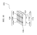
- Each solar cell 101 includes semiconductor substrate 107 having a PN junction, antireflection film 108 and front-surface-side electrode 109 which are formed on a front surface of semiconductor substrate 107, and rear-surface-side electrode 110 formed on a rear surface of semiconductor substrate 107.
- Front-surface-side electrode 109 includes a plurality of finger-shaped collector electrodes 109a and bus bar electrodes 109b each orthogonally crossing collector electrodes 109a.
- rear-surface-side electrode 110 includes metal-film-shaped collector electrode 110a and bus bar electrodes 110b.
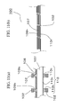
- Fig. 11(a) is a cross-sectional view taken along the A-A' line in Fig. 9 for explaining the connection between solar cell 101 and conductive connecting members 102.
- Fig. 11 (b) is a cross-sectional view taken along the B-B' line in Fig. 9 for explaining the connection between solar cells 101 in solar cell module 100 and conductive connecting members 102.
- Each of conductive connecting members 102 connects one of bus bar electrodes 109b of one of solar cells 101 with one of bus bar electrodes 110b of an adjacent one of solar cells 101. Thereby, adjacent solar cells 101 are electrically connected to each other.
- Patent Document 1 Japanese Patent Application Publication No. 2006-13406
- Patent Document 1 discloses conductive connecting members each having an uneven surface or a texture surface on the light-receiving surface side.
- each conductive connecting member has one surface having an uneven shape and the other surface having a flat shape.
- the conductive connecting member is connected to a bus bar electrode on the front surface side of a solar cell and a bus bar electrode on the rear surface side of a solar cell wherein both of the bus bar electrodes having the same width, the contact area between the one surface of the connecting member and the bus bar electrodes on the front surface side is smaller than the contact area between the other surface of the connecting member and the bus bar electrode on the rear surface side.
- a solar cell module includes: a solar cells each including a first bus bar electrode on one principal surface and a second bus bar electrode on an opposite principal surface; and a conductive connecting member electrically connecting the first bus bar electrode or the second bus bar electrode of one of the solar cells with the first bus bar electrode or the second bus bar electrode of another solar cell.
- the conductive connecting member includes a first principal surface in an uneven shape and a second principal surface in a flat shape which is opposite from the first principal surface.
- the first bus bar electrode is connected to the second principal surface of the conductive connecting member.
- the second bus bar electrode is connected to the first principal surface of the conductive connecting member.
- the second bus bar electrode has a larger region width in a short-side direction of the conductive connecting member than that of the first bus bar electrode.
- the solar cell module according to the invention can reduce stress to be applied to the solar cell.
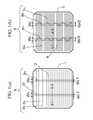
- Fig. 1(a) illustrates a front-side plan view of solar cell 1.
- Fig. 1(b) illustrates a rear-side plan view of solar cell 1.
- solar cell 1 includes transparent conductive film layer 2 and front-surface-side electrode 3 which are formed in this order on the front surface side.
- Front-surface-side electrode 3 is formed by causing an epoxy-based thermosetting silver paste to be formed on transparent conductive film layer 2 by screen printing, offset printing, or the like, and then to be heated at 200°C to thereby be hardened.
- Front-surface-side electrode 3 includes a plurality of finger electrodes 3a and two bus bar electrodes 3b.
- the plurality of finger electrodes 3a are formed in an almost entire region of a front surface of transparent conductive film layer 2.
- Finger electrodes 3a each have a fine-line shape and are arranged in parallel to each other.
- each finger electrode 3a is shaped into a line having a thickness of 25 ⁇ m to 60 ⁇ m and a line width of 50 ⁇ m to 120 ⁇ m, and is arranged at intervals of 2 mm.
- Each of two bus bar electrodes 3b is integrally formed so as to orthogonally cross and be connected to the plurality of finger electrodes 3a on the front surface of transparent conductive film layer 2.
- Each bus bar electrode 3b is shaped into a fine line.
- bus bar electrode 3b is shaped into a line having a thickness of 25 ⁇ m to 60 ⁇ m and a line width of 80 ⁇ m to 500 ⁇ m.
- a width of each conductive connecting member in a short-side direction is defined as Ws
- a width of each bus bar electrode 3b with respect to width Ws is defined as region width Wr1.
- solar cell 1 includes transparent conductive film layer 4 and rear-surface-side electrode 5 which are formed in this order on the rear surface side.
- Rear-surface-side electrode 5 comprises a plurality of finger electrodes 5a and two zig-zag bus bar electrodes 5b.
- each adjacent finger electrodes 5a of rear-surface-side electrode 5 are formed at a narrower interval than an interval between each adjacent finger electrodes 3a of front-surface-side electrode 3.
- Each of zig-zag bus bar electrodes 5b is integrally formed to be connected to the plurality of finger electrodes 5a on the rear surface of transparent conductive film layer 4.
- Each bus bar electrode 5b is shaped into a fine line and a zig-zag pattern having a plurality of fine-line-shaped straight sections.
- each bus bar electrode 5b has a thickness of 10 ⁇ m to 30 ⁇ m and a line width of 80 ⁇ m to 500 ⁇ m.
- a width of each bus bar electrode 5b in the short-side direction with respect to width Ws of each conductive connecting member is defined as region width Wr2, as for the front surface side.
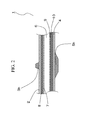
- Fig. 2 is a projection view illustrating a cross section taken along the A1-A1' line in Figs. 1(a) and 1(b) .
- Solar cell 1 includes n-type single crystal silicon substrate 6, i-type amorphous silicon layer 7, p-type amorphous silicon layer 8, transparent conductive film layer 2, bus bar electrodes 3b, i-type amorphous silicon layer 9, n-type amorphous silicon layer 10, transparent conductive film layer 4, and bus bar electrodes 5b.
- N-type single crystal silicon substrate 6 has an approximately square flat shape having sides of about 125 mm and a thickness of 100 ⁇ m to 300 ⁇ m, for example.
- Solar cell 1 includes, on the front-surface side, i-type amorphous silicon layer 7, p-type amorphous silicon layer 8, and transparent conductive film layer 2 which are formed in this order on a texture-structured front surface of n-type single crystal silicon substrate 6.
- front-surface-side electrode 3 is formed on transparent conductive film layer 2 in a predetermined location.
- solar cell 1 includes, on the rear surface side, i-type amorphous silicon layer 9, n-type amorphous silicon layer 10, and transparent conductive film layer 4 which are formed in this order on a texture-structured rear surface of n-type single crystal silicon substrate 6.
- rear-surface-side electrode 5 is formed on transparent conductive film layer 4 in a predetermined location.
- the solar cell may has reversed polarities with respect to those in the aforementioned solar cell 1, for example, the solar cell may have an n-type amorphous silicon layer on the front surface side and a p-type amorphous silicon layer on the rear surface side.
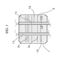
- Fig. 3 is a front-side plan view for explaining connection between solar cell 1 and conductive connecting members 11.
- Each of conductive connecting members 11 is connected to a corresponding one of bus bar electrodes 3b on the front surface side of solar cell 1 by using adhesive 12 containing a resin.
- Fig. 4(a) is a perspective view of conductive connecting member 11
- Fig. 4 (b) is a top view of conductive connecting member 11.
- Conductive connecting member 11 includes, on the upper side thereof, corrugated portion 11a or an uneven portion having a structure in which a plurality of triangles having the same shape regularly arranged side by side in a cross section in the short-side direction of conductive connecting member 11 and the triangles parallelly extend in a longitudinal direction of conductive connecting member 11.
- conductive connecting member 11 has flat surface 11b on a lower side thereof.
- Conductive connecting member 11 is a copper wire having width Ws of 0.8 mm to 1.5 mm and thickness t of approximately 150 ⁇ m to 300 ⁇ m.
- Corrugated portion 11a or a texture portion has a stripe pattern such that each of the triangle shapes of corrugated portion 11a has a bottom side of 100 ⁇ m and a height of 20 ⁇ m.
- conductive connecting member 11 may be coated with a conductive layer of Sn-Ag-Cu, Ag or the like by a plating method, a dip method, or the like to make flat the entire lower surface of conductive connecting member 11 in such a manner that a periphery of conductive connecting member 11 is covered.
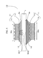
- Fig. 5 is a cross-sectional view taken along the A2-A2' line in Fig. 3 , which is a projection view illustrating connection between one of conductive connecting members 11 and a corresponding one of bus bar electrodes 3b and connection between another one of conductive connecting members 11 and a corresponding one of bus bar electrodes 5b.
- the connection structure of conductive connecting members 11 is described in detail with reference to the projection view
- each conductive connecting member 11 connects one of bus bar electrodes 3b on the front surface side of one of solar cells 1 and one of bus bar electrodes 5b on the rear surface side of another one of solar cells 1 adjacent to the one of solar cells 1.
- adhesive 12 is an epoxy-based thermosetting resin which is hardened by being heated at about 200°C.
- Adhesive 12 is disposed between and connected to conductive connecting member 11 and front-surface-side electrode 3. For example, the connection is performed by disposing conductive connecting member 11 on adhesive 12 with adhesive 12 being disposed on bus bar electrode 3b. Adhesive 12 is also disposed between and connected to conductive connecting member 11 and rear-surface-side electrode 5. For example, the connection is performed by disposing conductive connecting member 11 on adhesive 12 with adhesive 12 being disposed on bus bar electrode 5b.
- Conductive connecting members 11 are thermo-compression bonded onto bus bar electrodes 3b and 5b at about 2 MPa and about 200°C.
- region width Wr2 of rear surface side bus bar electrode 5b of solar cell 1 is larger than region width Wr1 of front surface side bus bar electrode 3b.
- This structure can reduce a difference between a contact area of front surface side bus bar electrode 3b to flat shape 11b of conductive connecting member 11 and a contact area of rear surface side bus bar electrode 5b to corrugated portion 11a of conductive connecting member 11.
- concentration of stress to each solar cell 1 can be reduced. Accordingly, this can prevent conductive connecting members 11 from coming off bus bar electrodes 3b or 5b.
- region width Wr1 of linear-shaped bus bar electrode 3b is smaller than width Ws of conductive connecting member 11 in this embodiment.
- Bus bar electrode 3b is exposed from both widthwise sides of conductive connecting member 11.
- bus bar electrode 3b When conductive connecting member 11 has width Ws of 1 mm, bus bar electrode 3b has a line width of 300 ⁇ m and region width Wr1 of 0.8 mm, for example.
- flat shape 11b of conductive connecting member 11 is connected to bus bar electrode 3b.
- This structure stabilizes the connection of fine-line-shaped bus bar electrode 3b formed of a reduced volume of the electrode material, because the contact surface of conductive connecting member 11 to bus bar electrode 3b is flat shape 11b.
- region width Wr2 of zig-zag bus bar electrode 5b is larger than width Ws of conductive connecting member 11.
- Bus bar electrode 5b is exposed from both widthwise sides of conductive connecting member 11.
- region width Wr2 of bus bar electrode 5b is preferably equal to or larger than a value obtained by adding, to width Ws of conductive connecting member 11, a value of accuracy allowance in disposing conductive connecting member 11 on bus bar electrode 5b in a manufacturing process and a value of accuracy allowance in forming an electrode for bus bar electrode 5b.
- bus bar electrode 5b may have the line width of 300 ⁇ m and the region width of 1.5 mm, for example.
- corrugated portion 11a of conductive connecting member 11 is connected to zig-zag bus bar electrode 5b having the region width of Wr2.
- This structure consequently stabilizes the connection between conductive connecting member 11 and bar electrode 5b, even though the contact surface of conductive connecting member 11 to bas bar electrode 5b has corrugated portion 11a. This is because region width Wr2 of zig-zag bus bar electrode 5b is larger than width Ws of conductive connecting member 11.
- bus bar electrode 3b having region width Wr1 is not exposed from both ends of width Ws of conductive connecting member 11. Thus, a decreased output due to light block can be prevented.
- bus bar electrode 5b having region width Wr2 is exposed from width Ws of conductive connecting member 11.
- bus bar electrode 5b having region width Wr2 functions as a pad (a reinforcing member). Hence, bus bar electrode 5b absorbs the stress applied from conductive connecting member 11 to bus bar electrode 3b, so that solar cell 1 can be prevented from cracking.
- Such solar cell 1 is electrically connected to another solar cell 1 with conductive connecting member 11 located in between. Thereafter, a known modularization process is performed, so that solar cell module 13 as shown in Fig. 10 is completed.
- Fig. 6 illustrates three types of shapes of bus bar electrodes on the front surface side of solar cell 1 according to other embodiments.
- Fig. 7 illustrates two types of shapes of bus bar electrodes on the front surface side of solar cell 1 according to still other embodiments.
- the bus bar electrodes on the front surface side may be four linear-shaped bus bar electrodes 30b, wavy-shaped bus bar electrodes 300b, or the like.
- region width Wr1 of each of front-side bus bar electrodes 30b, 300b, and 3000b is also smaller than width Ws of a corresponding one of conductive connecting members 11, and each of bus bar electrodes 30b, 300b, and 3000b is not exposed from both widthwise ends of corresponding conductive connecting member 11.
- bus bar electrode 30b are formed into four lines each having a thickness of 25 ⁇ m to 60 ⁇ m and a line width of 80 ⁇ m to 200 ⁇ m.
- each conductive connecting member 11 has width Ws of 1 mm
- each bus bar electrode 30b has a line width of 100 ⁇ m and region width Wr1 of 0.8 mm, for example.
- Each of bus bar electrodes 300b is formed into a wavy shape having a thickness of 25 ⁇ m to 60 ⁇ m and a line width of 80 ⁇ m to 500 ⁇ m.
- each bus bar electrode 300b has a line width of 80 ⁇ m and region width Wr1 of 0.8 mm, for example.
- Each of bus bar electrodes 3000b is formed into a zig-zag shape having a thickness of 25 ⁇ m to 60 ⁇ m and a line width of 80 ⁇ m to 500 ⁇ m.
- bus bar electrode 3000b has a line width of 80 ⁇ m and region width Wr1 of 0.8 mm, for example.
- the bus bar electrodes on the rear surface side may be strip-shaped bus bar electrodes 50b, wavy-shaped bus bar electrodes 500b, or the like.
- region width Wr2 of each of rear-side bus bar electrodes 50b and 500b is also larger than width Ws of corresponding conductive connecting member 11, and each of bus bar electrodes 50b and 500b is exposed from both widthwise ends of corresponding conductive connecting member 11.
- each of region widths Wr2 of bus bar electrodes 50b and 500b are preferably equal to or larger than a value obtained by adding, to width Ws of conductive connecting member 11, a value of accuracy allowance in disposing conductive connecting member 11 on corresponding bus bar electrode 5b or 500b in a manufacturing process and a value of accuracy allowance in forming an electrode for bus bar electrode 5b or 500b.
- Each bus bar electrode 50b is formed into a wide strip shape having a thickness of 10 ⁇ m to 30 ⁇ m and a line width of 0.8 mm to 3 mm.
- bus bar electrode 50b has a line width of 1.5 mm and region width Wr2 of 1.5 mm, for example.
- Each bus bar electrode 500b is formed into a wavy shape having a thickness of 10 ⁇ m to 30 ⁇ m and a line width of 80 ⁇ m to 500 ⁇ m.
- bus bar electrode 500b for example has a line width of 300 ⁇ m and region width Wr2 of 1.5 mm.
- bus bar electrodes each having region width Wr1 on the front surface side and the bus bar electrodes having region width Wr2 on the rear surface side in the above embodiments can be combined appropriately.
- the bus bar electrodes on the front surface side of one of the solar cells and a corresponding one of the bus bar electrodes on the rear surface side of an adjacent one of the solar cells are connected in series.
- the connection of the adjacent solar cells is not limited to those in the above embodiments.
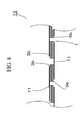
- a structure as in Fig. 8 may be employed.
- the same reference numerals denote the same or similar components to those in the above embodiments.
- Solar cell module 13 shown in Fig. 8 has a device configuration in which polarities of adjacent solar cells 1 are reverse to each other.
- conductive connecting members 11 connect bus bar electrodes of adjacent solar cells 1 to each other, and also on the rear surface side, conductive connecting members 11 connect bus bar electrodes of adjacent solar cells 1 to each other.
- a flat lower surface of each conductive connecting member 11 is connected to a corresponding one of bus bar electrodes 3b on the front surface side
- an corrugated upper surface of each of conductive connecting member 11 is connected to a corresponding one of bus bar electrodes 5b on the rear surface side.
- bus bar electrodes of each solar cell and the conductive connecting members are connected by using the adhesive in the aforementioned embodiments, but may be connected by melting and hardening of solder.
- an insulating adhesive may be used as the adhesive.
- a conductive adhesive may be used.
- the resin is not limited to the epoxy-based thermosetting resin, and an appropriate resin is usable.
- the adhesive may contain conductive particles or the like such as Ni or Ag, may contain a non-conductive material having non-conductive particles or the like such as Silicon oxide, may contain both of these materials, and may contain neither of these materials.
- the invention is not limited to the structure of the solar cell shown in Fig. 2 and appropriately applicable to various solar cells such as a polycrystalline solar cell.
Landscapes
- Photovoltaic Devices (AREA)
Abstract
Description
- The invention relates to a solar cell module.
- A solar cell module generally has a structure in which a plurality of cells are electrically connected in series to thereby enhance output therefrom.
- A structure of
solar cell module 100 is described with reference toFig. 9 .Solar cell module 100 includessolar cell groups 103 having a plurality ofsolar cells 101 connected in series by using conductive connectingmember 102.Solar cell groups 103 are connected to each other in such manner that each adjacentsolar cell groups 103 are soldered by using connectingmember - With this structure, the series connection of the plurality of
solar cells 101 leads to enhanced output fromsolar cell module 100. - In addition, outermost
solar cell groups 103 are electrically connected to L-shaped connecting members (output extraction connecting members) 106 for extracting electric output fromsolar cell module 100. - As described above,
solar cells 101 need to be electrically connected to one another by using conductive connectingmembers 102. Hereinbelow, the connection structure is described in detail. - First, a structure of each
solar cell 101 is described in detail with reference toFig. 10 . Eachsolar cell 101 includessemiconductor substrate 107 having a PN junction,antireflection film 108 and front-surface-side electrode 109 which are formed on a front surface ofsemiconductor substrate 107, and rear-surface-side electrode 110 formed on a rear surface ofsemiconductor substrate 107. - Front-surface-
side electrode 109 includes a plurality of finger-shaped collector electrodes 109a andbus bar electrodes 109b each orthogonally crossingcollector electrodes 109a. In addition, rear-surface-side electrode 110 includes metal-film-shaped collector electrode 110a andbus bar electrodes 110b. - Next, the connection structure using conductive connecting
members 102 is described in detail with reference toFigs. 11(a) and 11(b). Fig. 11(a) is a cross-sectional view taken along the A-A' line inFig. 9 for explaining the connection betweensolar cell 101 and conductive connectingmembers 102.Fig. 11 (b) is a cross-sectional view taken along the B-B' line inFig. 9 for explaining the connection betweensolar cells 101 insolar cell module 100 and conductive connectingmembers 102. - Each of conductive connecting
members 102 connects one ofbus bar electrodes 109b of one ofsolar cells 101 with one ofbus bar electrodes 110b of an adjacent one ofsolar cells 101. Thereby, adjacentsolar cells 101 are electrically connected to each other. - Patent Document 1: Japanese Patent Application Publication No.
2006-13406 - Here,
Patent Document 1 discloses conductive connecting members each having an uneven surface or a texture surface on the light-receiving surface side. - That is, each conductive connecting member has one surface having an uneven shape and the other surface having a flat shape. When the conductive connecting member is connected to a bus bar electrode on the front surface side of a solar cell and a bus bar electrode on the rear surface side of a solar cell wherein both of the bus bar electrodes having the same width, the contact area between the one surface of the connecting member and the bus bar electrodes on the front surface side is smaller than the contact area between the other surface of the connecting member and the bus bar electrode on the rear surface side.
- Accordingly, stress is applied to the solar cell, and the conductive connecting member might come off the solar cell.
- A solar cell module according to the invention includes: a solar cells each including a first bus bar electrode on one principal surface and a second bus bar electrode on an opposite principal surface; and a conductive connecting member electrically connecting the first bus bar electrode or the second bus bar electrode of one of the solar cells with the first bus bar electrode or the second bus bar electrode of another solar cell. The conductive connecting member includes a first principal surface in an uneven shape and a second principal surface in a flat shape which is opposite from the first principal surface. The first bus bar electrode is connected to the second principal surface of the conductive connecting member. The second bus bar electrode is connected to the first principal surface of the conductive connecting member. The second bus bar electrode has a larger region width in a short-side direction of the conductive connecting member than that of the first bus bar electrode.
- The solar cell module according to the invention can reduce stress to be applied to the solar cell.
-
- [
Fig. 1] Fig. 1(a) illustrates a front-side plan view of a solar cell.Fig. 1(b) illustrates a rear-side plan view of the solar cell. - [
Fig. 2] Fig. 2 is a projection view illustrating a cross section taken along the A1-A1' line inFigs. 1(a) and 1(b) . - [
Fig. 3] Fig. 3 is a front-side plan view for explaining connection between the solar cell and conductive connecting members. - [
Fig. 4] Figs. 4 (a) and 4(b) illustrate a structure of each of the conductive connecting members according to one embodiment of the invention. - [
Fig. 5] Fig. 5 is a projection view showing a cross-section taken along the A2-A2' line inFig. 3 , illustrating connection structure between conductive connecting members and bus bar electrodes. - [
Fig. 6] Figs. 6(a1), 6(a2), and 6(a3) are front-side plan views illustrating shapes of the bus bar electrodes on the front surface side according to other embodiments of the invention. - [
Fig. 7] Fig. 7(b1) and 7(b2) are rear-side plan views illustrating shapes of the bus bar electrodes on the rear surface side according to still other embodiments of the invention. - [
Fig. 8] Fig. 8 is a partial cross-sectional view of a solar cell module according to yet another embodiment of the invention. - [
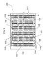
Fig. 9] Fig. 9 is a front-side plan view for explaining a conventional solar cell module. - [
Fig. 10] Fig. 10 is a perspective view of one of solar cells in the conventional solar cell module. - [
Fig. 11] Fig. 11 (a) is a cross-sectional view for explaining connection between the solar cell and conductive connecting members, andFig. 11(b) is a cross-sectional view for explaining connection between the solar cells and the conductive connecting members in the conventional solar cell module. - Hereinbelow, a solar cell module according to one embodiment of the invention is described in detail by referring to the drawings.
- First, a structure of each of solar cells constituting the solar cell module is described in detail with reference to
Fig. 1 andFig. 2 . -
Fig. 1(a) illustrates a front-side plan view ofsolar cell 1.Fig. 1(b) illustrates a rear-side plan view ofsolar cell 1. - With reference to
Fig. 1(a) ,solar cell 1 includes transparentconductive film layer 2 and front-surface-side electrode 3 which are formed in this order on the front surface side. - Front-surface-
side electrode 3 is formed by causing an epoxy-based thermosetting silver paste to be formed on transparentconductive film layer 2 by screen printing, offset printing, or the like, and then to be heated at 200°C to thereby be hardened. - Front-surface-
side electrode 3 includes a plurality offinger electrodes 3a and twobus bar electrodes 3b. - The plurality of
finger electrodes 3a are formed in an almost entire region of a front surface of transparentconductive film layer 2.Finger electrodes 3a each have a fine-line shape and are arranged in parallel to each other. For example, eachfinger electrode 3a is shaped into a line having a thickness of 25 µm to 60 µm and a line width of 50 µm to 120 µm, and is arranged at intervals of 2 mm. - Each of two
bus bar electrodes 3b is integrally formed so as to orthogonally cross and be connected to the plurality offinger electrodes 3a on the front surface of transparentconductive film layer 2. Eachbus bar electrode 3b is shaped into a fine line. For example,bus bar electrode 3b is shaped into a line having a thickness of 25 µm to 60 µm and a line width of 80 µm to 500 µm. - Here, on the front surface side, a width of each conductive connecting member in a short-side direction is defined as Ws, and a width of each
bus bar electrode 3b with respect to width Ws is defined as region width Wr1. - With reference to
Fig. 1(b) ,solar cell 1 includes transparentconductive film layer 4 and rear-surface-side electrode 5 which are formed in this order on the rear surface side. - Rear-surface-
side electrode 5 comprises a plurality offinger electrodes 5a and two zig-zagbus bar electrodes 5b. - In this embodiment, each
adjacent finger electrodes 5a of rear-surface-side electrode 5 are formed at a narrower interval than an interval between eachadjacent finger electrodes 3a of front-surface-side electrode 3. - Each of zig-zag
bus bar electrodes 5b is integrally formed to be connected to the plurality offinger electrodes 5a on the rear surface of transparentconductive film layer 4. Eachbus bar electrode 5b is shaped into a fine line and a zig-zag pattern having a plurality of fine-line-shaped straight sections. For example, eachbus bar electrode 5b has a thickness of 10 µm to 30 µm and a line width of 80 µm to 500 µm. - In this embodiment, a width of each
bus bar electrode 5b in the short-side direction with respect to width Ws of each conductive connecting member is defined as region width Wr2, as for the front surface side. - Next, a cross-sectional structure of
solar cell 1 is described in detail with reference toFig. 2. Fig. 2 is a projection view illustrating a cross section taken along the A1-A1' line inFigs. 1(a) and 1(b) . -
Solar cell 1 includes n-type single crystal silicon substrate 6, i-typeamorphous silicon layer 7, p-typeamorphous silicon layer 8, transparentconductive film layer 2,bus bar electrodes 3b, i-typeamorphous silicon layer 9, n-typeamorphous silicon layer 10, transparentconductive film layer 4, andbus bar electrodes 5b. - N-type single crystal silicon substrate 6 has an approximately square flat shape having sides of about 125 mm and a thickness of 100 µm to 300 µm, for example.
-
Solar cell 1 includes, on the front-surface side, i-typeamorphous silicon layer 7, p-typeamorphous silicon layer 8, and transparentconductive film layer 2 which are formed in this order on a texture-structured front surface of n-type single crystal silicon substrate 6. In addition, front-surface-side electrode 3 is formed on transparentconductive film layer 2 in a predetermined location.
Likewise,solar cell 1 includes, on the rear surface side, i-typeamorphous silicon layer 9, n-typeamorphous silicon layer 10, and transparentconductive film layer 4 which are formed in this order on a texture-structured rear surface of n-type single crystal silicon substrate 6. In addition, rear-surface-side electrode 5 is formed on transparentconductive film layer 4 in a predetermined location. - Here, the solar cell may has reversed polarities with respect to those in the aforementioned
solar cell 1, for example, the solar cell may have an n-type amorphous silicon layer on the front surface side and a p-type amorphous silicon layer on the rear surface side. -
Fig. 3 is a front-side plan view for explaining connection betweensolar cell 1 and conductive connectingmembers 11. - Each of conductive connecting
members 11 is connected to a corresponding one ofbus bar electrodes 3b on the front surface side ofsolar cell 1 by using adhesive 12 containing a resin. - Here, a structure of each conductive connecting
member 11 is described in detail with reference toFigs. 4(a) and 4(b). Fig. 4(a) is a perspective view of conductive connectingmember 11, andFig. 4 (b) is a top view of conductive connectingmember 11. - Conductive connecting
member 11 includes, on the upper side thereof,corrugated portion 11a or an uneven portion having a structure in which a plurality of triangles having the same shape regularly arranged side by side in a cross section in the short-side direction of conductive connectingmember 11 and the triangles parallelly extend in a longitudinal direction of conductive connectingmember 11. In addition, conductive connectingmember 11 hasflat surface 11b on a lower side thereof. - Conductive connecting
member 11 is a copper wire having width Ws of 0.8 mm to 1.5 mm and thickness t of approximately 150 µm to 300 µm.Corrugated portion 11a or a texture portion has a stripe pattern such that each of the triangle shapes ofcorrugated portion 11a has a bottom side of 100 µm and a height of 20 µm. Note that conductive connectingmember 11 may be coated with a conductive layer of Sn-Ag-Cu, Ag or the like by a plating method, a dip method, or the like to make flat the entire lower surface of conductive connectingmember 11 in such a manner that a periphery of conductive connectingmember 11 is covered. - Next,
Fig. 5 is a cross-sectional view taken along the A2-A2' line inFig. 3 , which is a projection view illustrating connection between one of conductive connectingmembers 11 and a corresponding one ofbus bar electrodes 3b and connection between another one of conductive connectingmembers 11 and a corresponding one ofbus bar electrodes 5b. The connection structure of conductive connectingmembers 11 is described in detail with reference to the projection view - By using
adhesive 12, each conductive connectingmember 11 connects one ofbus bar electrodes 3b on the front surface side of one ofsolar cells 1 and one ofbus bar electrodes 5b on the rear surface side of another one ofsolar cells 1 adjacent to the one ofsolar cells 1. - For example, adhesive 12 is an epoxy-based thermosetting resin which is hardened by being heated at about 200°C.
-
Adhesive 12 is disposed between and connected to conductive connectingmember 11 and front-surface-side electrode 3. For example, the connection is performed by disposing conductive connectingmember 11 on adhesive 12 with adhesive 12 being disposed onbus bar electrode 3b.Adhesive 12 is also disposed between and connected to conductive connectingmember 11 and rear-surface-side electrode 5. For example, the connection is performed by disposing conductive connectingmember 11 on adhesive 12 with adhesive 12 being disposed onbus bar electrode 5b. - Conductive connecting
members 11 are thermo-compression bonded ontobus bar electrodes - In this embodiment, region width Wr2 of rear surface side
bus bar electrode 5b ofsolar cell 1 is larger than region width Wr1 of front surface sidebus bar electrode 3b. This structure can reduce a difference between a contact area of front surface sidebus bar electrode 3b toflat shape 11b of conductive connectingmember 11 and a contact area of rear surface sidebus bar electrode 5b tocorrugated portion 11a of conductive connectingmember 11. As the result, whensolar cells 1 are modularized intosolar cell module 13, concentration of stress to eachsolar cell 1 can be reduced. Accordingly, this can prevent conductive connectingmembers 11 from coming offbus bar electrodes - In addition, on the front surface side, region width Wr1 of linear-shaped
bus bar electrode 3b is smaller than width Ws of conductive connectingmember 11 in this embodiment.Bus bar electrode 3b is exposed from both widthwise sides of conductive connectingmember 11. - When conductive connecting
member 11 has width Ws of 1 mm,bus bar electrode 3b has a line width of 300 µm and region width Wr1 of 0.8 mm, for example. - Moreover, on the front surface side,
flat shape 11b of conductive connectingmember 11 is connected tobus bar electrode 3b. This structure stabilizes the connection of fine-line-shapedbus bar electrode 3b formed of a reduced volume of the electrode material, because the contact surface of conductive connectingmember 11 tobus bar electrode 3b isflat shape 11b. - In this embodiment, on the rear surface side, region width Wr2 of zig-zag
bus bar electrode 5b is larger than width Ws of conductive connectingmember 11.Bus bar electrode 5b is exposed from both widthwise sides of conductive connectingmember 11. It should be noted that region width Wr2 ofbus bar electrode 5b is preferably equal to or larger than a value obtained by adding, to width Ws of conductive connectingmember 11, a value of accuracy allowance in disposing conductive connectingmember 11 onbus bar electrode 5b in a manufacturing process and a value of accuracy allowance in forming an electrode forbus bar electrode 5b. In the case where the conductive connecting member has width Ws of 1 mm,bus bar electrode 5b may have the line width of 300 µm and the region width of 1.5 mm, for example. - Meanwhile, on the rear surface side,
corrugated portion 11a of conductive connectingmember 11 is connected to zig-zagbus bar electrode 5b having the region width of Wr2. This structure consequently stabilizes the connection between conductive connectingmember 11 andbar electrode 5b, even though the contact surface of conductive connectingmember 11 to bas barelectrode 5b has corrugatedportion 11a. This is because region width Wr2 of zig-zagbus bar electrode 5b is larger than width Ws of conductive connectingmember 11. - As described above, on the light-receiving side of
solar cell 1,bus bar electrode 3b having region width Wr1 is not exposed from both ends of width Ws of conductive connectingmember 11. Thus, a decreased output due to light block can be prevented. - In contrast, since, on an opposite side of
solar cell 1 opposed from the light-receiving side, since it is less likely to occur a decreased output due to light block,bus bar electrode 5b having region width Wr2 is exposed from width Ws of conductive connectingmember 11. - In connecting such
bus bar electrodes members 11,bus bar electrode 5b having region width Wr2 functions as a pad (a reinforcing member). Hence,bus bar electrode 5b absorbs the stress applied from conductive connectingmember 11 tobus bar electrode 3b, so thatsolar cell 1 can be prevented from cracking. - Such
solar cell 1 is electrically connected to anothersolar cell 1 with conductive connectingmember 11 located in between. Thereafter, a known modularization process is performed, so thatsolar cell module 13 as shown inFig. 10 is completed. - In
solar cell module 13, among light incident on the light-receiving side, light that reachescorrugated portions 11a of conductive connectingmembers 11 is reflected efficiently fromcorrugated portion 11a toward a filling material and a front surface side cover, which are not shown in the drawings. Hence, an amount of light reflected back from the filling material or the front surface side cover tosolar cell 1 increases, and an amount of light incident onsolar cell 1 consequently increases. Thus, output fromsolar cell 1 is enhanced. - Hereinbelow, other embodiments of the invention are described in detail with reference to
Figs. 6 and7 . -
Fig. 6 illustrates three types of shapes of bus bar electrodes on the front surface side ofsolar cell 1 according to other embodiments.Fig. 7 illustrates two types of shapes of bus bar electrodes on the front surface side ofsolar cell 1 according to still other embodiments. - In these embodiments, the bus bar electrodes on the front surface side may be four linear-shaped
bus bar electrodes 30b, wavy-shapedbus bar electrodes 300b, or the like. - In these configuration, region width Wr1 of each of front-side
bus bar electrodes members 11, and each ofbus bar electrodes member 11. For example,bus bar electrode 30b are formed into four lines each having a thickness of 25 µm to 60 µm and a line width of 80 µm to 200 µm. When each conductive connectingmember 11 has width Ws of 1 mm, eachbus bar electrode 30b has a line width of 100 µm and region width Wr1 of 0.8 mm, for example. Each ofbus bar electrodes 300b is formed into a wavy shape having a thickness of 25 µm to 60 µm and a line width of 80 µm to 500 µm. When conductive connectingmember 11 has width Ws of 1 mm, eachbus bar electrode 300b has a line width of 80 µm and region width Wr1 of 0.8 mm, for example. Each ofbus bar electrodes 3000b is formed into a zig-zag shape having a thickness of 25 µm to 60 µm and a line width of 80 µm to 500 µm. When conductive connectingmember 11 has width Ws of 1 mm,bus bar electrode 3000b has a line width of 80 µm and region width Wr1 of 0.8 mm, for example. - In these embodiments, the bus bar electrodes on the rear surface side may be strip-shaped
bus bar electrodes 50b, wavy-shapedbus bar electrodes 500b, or the like. - In these configuration, region width Wr2 of each of rear-side
bus bar electrodes member 11, and each ofbus bar electrodes member 11. It should be noted that each of region widths Wr2 ofbus bar electrodes member 11, a value of accuracy allowance in disposing conductive connectingmember 11 on correspondingbus bar electrode bus bar electrode bus bar electrode 50b is formed into a wide strip shape having a thickness of 10 µm to 30 µm and a line width of 0.8 mm to 3 mm. When conductive connectingmember 11 has width Ws of 1 mm,bus bar electrode 50b has a line width of 1.5 mm and region width Wr2 of 1.5 mm, for example. Eachbus bar electrode 500b is formed into a wavy shape having a thickness of 10 µm to 30 µm and a line width of 80 µm to 500 µm. When conductive connectingmember 11 has width Ws of 1 mm,bus bar electrode 500b for example has a line width of 300 µm and region width Wr2 of 1.5 mm. - In the invention, the bus bar electrodes each having region width Wr1 on the front surface side and the bus bar electrodes having region width Wr2 on the rear surface side in the above embodiments can be combined appropriately.
- Meanwhile, in the above embodiments, the bus bar electrodes on the front surface side of one of the solar cells and a corresponding one of the bus bar electrodes on the rear surface side of an adjacent one of the solar cells are connected in series. However, the connection of the adjacent solar cells is not limited to those in the above embodiments.
- For example, a structure as in
Fig. 8 may be employed. Note that inFig. 8 , the same reference numerals denote the same or similar components to those in the above embodiments. -
Solar cell module 13 shown inFig. 8 has a device configuration in which polarities of adjacentsolar cells 1 are reverse to each other. On the front surface side, conductive connectingmembers 11 connect bus bar electrodes of adjacentsolar cells 1 to each other, and also on the rear surface side, conductive connectingmembers 11 connect bus bar electrodes of adjacentsolar cells 1 to each other. Also in this case, a flat lower surface of each conductive connectingmember 11 is connected to a corresponding one ofbus bar electrodes 3b on the front surface side, and an corrugated upper surface of each of conductive connectingmember 11 is connected to a corresponding one ofbus bar electrodes 5b on the rear surface side. - Note that the above embodiments are presented only to facilitate understanding of the invention, and thus not to provide limited interpretation of the invention. The invention can be modified or improved without departing from the gist thereof, and the equivalents of the invention are also included in the invention.
- For example, the bus bar electrodes of each solar cell and the conductive connecting members are connected by using the adhesive in the aforementioned embodiments, but may be connected by melting and hardening of solder.
- In addition, an insulating adhesive may be used as the adhesive. Alternatively, a conductive adhesive may be used. Moreover, the resin is not limited to the epoxy-based thermosetting resin, and an appropriate resin is usable.
- Further, the adhesive may contain conductive particles or the like such as Ni or Ag, may contain a non-conductive material having non-conductive particles or the like such as Silicon oxide, may contain both of these materials, and may contain neither of these materials.
- The invention is not limited to the structure of the solar cell shown in
Fig. 2 and appropriately applicable to various solar cells such as a polycrystalline solar cell. -
1 solar cell 2, 4 transparent conductive film layer 3 front-surface- side electrode 3a finger electrode 3b, 30b, 300b, 3000b bus bar electrode 5 rear-surface- side electrode 5a finger electrode 5b, 50b, 500b bus bar electrode 11 conductive connecting member 12 adhesive 13 solar cell module Wr1 region width of bus bar electrode on front surface side Wr2 region width of bus bar electrode on rear surface side Ws width of conductive connecting member
Claims (6)
- A solar cell module comprises:solar cells each including a first bus bar electrode on one principal surface and a second bus bar electrode on an opposite principal surface; anda conductive connecting member electrically connecting the first bus bar electrode or the second bus bar electrode of one of the solar cells with the first bus bar electrode or the second bus bar electrode of another solar cell, whereinthe conductive connecting member includes a first principal surface in an uneven shape and a second principal surface in a flat shape which is opposite from the first principal surface,the first bus bar electrode is connected to the second principal surface of the conductive connecting member,the second bus bar electrode is connected to the first principal surface of the conductive connecting member,the second bus bar electrode has a larger region width in a short-side direction of the conductive connecting member than that of the first bus bar electrode.
- The solar cell module according to claim 1, wherein
the uneven shape comprises a plurality of concave-convex portions that extend in a longitudinal direction of the conductive connecting member. - The solar cell module according to any one of claims 1 and 2, wherein the first bus bar electrode has any one of a linear pattern, a wavy shape, and a zig-zag shape.
- The solar cell module according to any one of claims 1 to 3, wherein the second bus bar electrode has any one of a zig-zag shape, a wavy shape, and a strip shape.
- The solar cell module according to any one of claims 1 to 4, wherein
the one principal surface is located on a light-receiving surface side of the solar cell module, and
the opposite principal surface is located on a side opposite from the light-receiving surface side. - The solar cell module according to any one of claims 1 to 5, wherein
the first principal surface is located on a light-receiving surface side of the solar cell module, and
the second principal surface is located on a side opposite from the light-receiving surface side.
Applications Claiming Priority (2)
| Application Number | Priority Date | Filing Date | Title |
|---|---|---|---|
| JP2010150113 | 2010-06-30 | ||
| PCT/JP2011/064251 WO2012002216A1 (en) | 2010-06-30 | 2011-06-22 | Solar cell module |
Publications (2)
| Publication Number | Publication Date |
|---|---|
| EP2590226A1 true EP2590226A1 (en) | 2013-05-08 |
| EP2590226A4 EP2590226A4 (en) | 2015-06-17 |
Family
ID=45401936
Family Applications (1)
| Application Number | Title | Priority Date | Filing Date |
|---|---|---|---|
| EP11800681.6A Withdrawn EP2590226A4 (en) | 2010-06-30 | 2011-06-22 | SOLAR CELL MODULE |
Country Status (4)
| Country | Link |
|---|---|
| US (1) | US8969708B2 (en) |
| EP (1) | EP2590226A4 (en) |
| JP (1) | JP5879512B2 (en) |
| WO (1) | WO2012002216A1 (en) |
Cited By (3)
| Publication number | Priority date | Publication date | Assignee | Title |
|---|---|---|---|---|
| WO2017027769A1 (en) * | 2015-08-13 | 2017-02-16 | 3M Innovative Properties Company | Photovoltaic cell with frontside busbar tape on narrow front busbars |
| WO2018031439A1 (en) * | 2016-08-12 | 2018-02-15 | 3M Innovative Properties Company | Photovoltaic cell with frontside busbar tape on narrow dual front busbars |
| CN108541348A (en) * | 2016-04-14 | 2018-09-14 | 株式会社钟化 | Wiring material used for solar batteries and solar cell module |
Families Citing this family (10)
| Publication number | Priority date | Publication date | Assignee | Title |
|---|---|---|---|---|
| DE102012109777A1 (en) * | 2012-10-15 | 2014-04-17 | Heliatek Gmbh | Method for printing optoelectronic components with busbars |
| WO2014132573A1 (en) * | 2013-02-28 | 2014-09-04 | 三洋電機株式会社 | Solar cell module production method |
| KR20140114529A (en) * | 2013-03-18 | 2014-09-29 | 현대중공업 주식회사 | Solar cell module with ribbon reflection structure |
| TWI447921B (en) * | 2013-05-31 | 2014-08-01 | Neo Solar Power Corp | Solar battery |
| TW201503391A (en) * | 2013-07-12 | 2015-01-16 | 茂迪股份有限公司 | Solar cell and its module |
| WO2017010384A1 (en) * | 2015-07-10 | 2017-01-19 | 日東電工株式会社 | Wiring structure, solar cell module, and solar cell |
| JP2018107211A (en) * | 2016-12-22 | 2018-07-05 | パナソニックIpマネジメント株式会社 | Solar cell module |
| JP6931591B2 (en) * | 2017-11-10 | 2021-09-08 | 株式会社カネカ | Solar cell module and manufacturing method of solar cell module |
| EP3544062A1 (en) * | 2018-03-22 | 2019-09-25 | LG Electronics Inc. | Interconnecting member for solar cell panel and solar cell panel including the same |
| CN117423754B (en) * | 2023-12-19 | 2024-04-23 | 天合光能股份有限公司 | Heterojunction battery and manufacturing method thereof, photovoltaic module and photovoltaic system |
Family Cites Families (17)
| Publication number | Priority date | Publication date | Assignee | Title |
|---|---|---|---|---|
| US4301322A (en) * | 1980-04-03 | 1981-11-17 | Exxon Research & Engineering Co. | Solar cell with corrugated bus |
| JP4462973B2 (en) * | 2004-03-16 | 2010-05-12 | シャープ株式会社 | SOLAR CELL, ITS MANUFACTURING METHOD, AND SOLAR CELL MODULE |
| JP4646558B2 (en) | 2004-06-29 | 2011-03-09 | 三洋電機株式会社 | Solar cell module |
| JP2006278710A (en) * | 2005-03-29 | 2006-10-12 | Kyocera Corp | Solar cell module and manufacturing method thereof |
| JP2007266262A (en) * | 2006-03-28 | 2007-10-11 | Sharp Corp | Solar cell with interconnector, solar cell module, and method for manufacturing solar cell module |
| JP5230089B2 (en) * | 2006-09-28 | 2013-07-10 | 三洋電機株式会社 | Solar cell module |
| JP4294048B2 (en) * | 2006-11-29 | 2009-07-08 | 三洋電機株式会社 | Solar cell module |
| JP4818095B2 (en) * | 2006-12-22 | 2011-11-16 | 三洋電機株式会社 | Solar cell |
| DE102007062689A1 (en) * | 2007-01-05 | 2008-07-10 | Cornelius Paul | Formation of contacting and current collecting electrodes for solar cells, involves arranging thin current collecting fingers parallely on front side of solar cell, relative to small distance, where series of individual junctures is formed |
| JP5153279B2 (en) * | 2007-09-25 | 2013-02-27 | 三洋電機株式会社 | Solar cell module |
| JP5147672B2 (en) * | 2008-01-31 | 2013-02-20 | 三洋電機株式会社 | Solar cell module and method for manufacturing solar cell module |
| CN101939847B (en) * | 2008-02-08 | 2012-04-25 | 三洋电机株式会社 | Solar cell module and solar cell |
| KR101195624B1 (en) * | 2008-03-31 | 2012-10-30 | 샤프 가부시키가이샤 | Solar cell, solar cell string and solar cell module |
| JP5306112B2 (en) * | 2009-02-17 | 2013-10-02 | 三洋電機株式会社 | Solar cell and solar cell module |
| JP5515367B2 (en) * | 2009-03-31 | 2014-06-11 | 三洋電機株式会社 | Solar cell, solar cell module and solar cell system |
| KR100990114B1 (en) * | 2009-07-07 | 2010-10-29 | 엘지전자 주식회사 | Solar cell module having interconnector and fabricating method the same |
| WO2011021655A1 (en) * | 2009-08-19 | 2011-02-24 | 三洋電機株式会社 | Solar battery, solar battery module and solar battery system |
-
2011
- 2011-06-22 WO PCT/JP2011/064251 patent/WO2012002216A1/en not_active Ceased
- 2011-06-22 EP EP11800681.6A patent/EP2590226A4/en not_active Withdrawn
- 2011-06-22 JP JP2012522572A patent/JP5879512B2/en active Active
-
2012
- 2012-12-17 US US13/716,329 patent/US8969708B2/en active Active
Cited By (6)
| Publication number | Priority date | Publication date | Assignee | Title |
|---|---|---|---|---|
| WO2017027769A1 (en) * | 2015-08-13 | 2017-02-16 | 3M Innovative Properties Company | Photovoltaic cell with frontside busbar tape on narrow front busbars |
| CN107980179A (en) * | 2015-08-13 | 2018-05-01 | 3M创新有限公司 | There is the photovoltaic cell of front busbar adhesive tape on narrow front busbar |
| CN107980179B (en) * | 2015-08-13 | 2020-10-16 | 3M创新有限公司 | Photovoltaic cell with front bus tape on narrow front bus |
| CN108541348A (en) * | 2016-04-14 | 2018-09-14 | 株式会社钟化 | Wiring material used for solar batteries and solar cell module |
| EP3444850A4 (en) * | 2016-04-14 | 2020-01-01 | Kaneka Corporation | Solar cell wiring member and solar cell module |
| WO2018031439A1 (en) * | 2016-08-12 | 2018-02-15 | 3M Innovative Properties Company | Photovoltaic cell with frontside busbar tape on narrow dual front busbars |
Also Published As
| Publication number | Publication date |
|---|---|
| US8969708B2 (en) | 2015-03-03 |
| EP2590226A4 (en) | 2015-06-17 |
| JPWO2012002216A1 (en) | 2013-08-22 |
| WO2012002216A1 (en) | 2012-01-05 |
| JP5879512B2 (en) | 2016-03-08 |
| US20130125953A1 (en) | 2013-05-23 |
Similar Documents
| Publication | Publication Date | Title |
|---|---|---|
| US8969708B2 (en) | Solar cell module | |
| CN108598186B (en) | solar cell module | |
| EP3525246B1 (en) | Solar cell module | |
| EP2669954A1 (en) | Solar cell and solar cell module | |
| CN110246919A (en) | Photovoltaic module and its manufacturing process comprising lapping photovoltaic tiles | |
| US10269992B2 (en) | Solar cell | |
| EP2738816B1 (en) | Solar cell, solar cell module, and method for producing solar cell | |
| JP6241763B2 (en) | Solar cell module and method for manufacturing solar cell module | |
| JP5944081B1 (en) | Solar cell, solar cell module, method for manufacturing solar cell, method for manufacturing solar cell module | |
| WO2012121348A1 (en) | Solar cell, solar cell module, method for producing solar cell, and method for producing solar cell module | |
| US20130247956A1 (en) | Solar cell module | |
| US10840402B2 (en) | Solar cell module | |
| US9048359B2 (en) | Solar cell module and manufacturing method thereof | |
| EP3151287A1 (en) | Solar cell module | |
| US20150083187A1 (en) | Solar cell module and solar cell module manufacturing method | |
| EP3147953A1 (en) | Solar cell module | |
| US20220310856A1 (en) | Optimised solar cell, solar cell module and method of manufacturing thereof | |
| JP6414550B2 (en) | Solar cell and method for manufacturing solar cell | |
| CN222261087U (en) | Welding strip, photovoltaic module and photovoltaic system | |
| KR102410785B1 (en) | Shingled high power module and manufacturing method thereof | |
| JP4809018B2 (en) | Solar cell | |
| CN121003041A (en) | For use in shingled solar cells | |
| JP2025182704A (en) | Solar cells and modules | |
| JP2024070097A (en) | Solar cell, stacked structure of solar cell, and method for manufacturing solar cell |
Legal Events
| Date | Code | Title | Description |
|---|---|---|---|
| PUAI | Public reference made under article 153(3) epc to a published international application that has entered the european phase |
Free format text: ORIGINAL CODE: 0009012 |
|
| 17P | Request for examination filed |
Effective date: 20130123 |
|
| AK | Designated contracting states |
Kind code of ref document: A1 Designated state(s): AL AT BE BG CH CY CZ DE DK EE ES FI FR GB GR HR HU IE IS IT LI LT LU LV MC MK MT NL NO PL PT RO RS SE SI SK SM TR |
|
| DAX | Request for extension of the european patent (deleted) | ||
| RA4 | Supplementary search report drawn up and despatched (corrected) |
Effective date: 20150518 |
|
| RIC1 | Information provided on ipc code assigned before grant |
Ipc: H01L 31/042 20140101AFI20150511BHEP Ipc: H01L 31/04 20140101ALI20150511BHEP Ipc: H01L 31/0224 20060101ALI20150511BHEP Ipc: H01L 31/05 20140101ALI20150511BHEP |
|
| RAP1 | Party data changed (applicant data changed or rights of an application transferred) |
Owner name: PANASONIC INTELLECTUAL PROPERTY MANAGEMENT CO., LT |
|
| STAA | Information on the status of an ep patent application or granted ep patent |
Free format text: STATUS: EXAMINATION IS IN PROGRESS |
|
| 17Q | First examination report despatched |
Effective date: 20171013 |
|
| GRAP | Despatch of communication of intention to grant a patent |
Free format text: ORIGINAL CODE: EPIDOSNIGR1 |
|
| STAA | Information on the status of an ep patent application or granted ep patent |
Free format text: STATUS: GRANT OF PATENT IS INTENDED |
|
| INTG | Intention to grant announced |
Effective date: 20210810 |
|
| STAA | Information on the status of an ep patent application or granted ep patent |
Free format text: STATUS: THE APPLICATION IS DEEMED TO BE WITHDRAWN |
|
| 18D | Application deemed to be withdrawn |
Effective date: 20211221 |