EP2590214A2 - Light-emitting module and luminaire - Google Patents
Light-emitting module and luminaire Download PDFInfo
- Publication number
- EP2590214A2 EP2590214A2 EP12181464.4A EP12181464A EP2590214A2 EP 2590214 A2 EP2590214 A2 EP 2590214A2 EP 12181464 A EP12181464 A EP 12181464A EP 2590214 A2 EP2590214 A2 EP 2590214A2
- Authority
- EP
- European Patent Office
- Prior art keywords
- light
- emitting
- sealing member
- emitting module
- led chips
- Prior art date
- Legal status (The legal status is an assumption and is not a legal conclusion. Google has not performed a legal analysis and makes no representation as to the accuracy of the status listed.)
- Withdrawn
Links
Images





Classifications
-
- H—ELECTRICITY
- H10—SEMICONDUCTOR DEVICES; ELECTRIC SOLID-STATE DEVICES NOT OTHERWISE PROVIDED FOR
- H10W—GENERIC PACKAGES, INTERCONNECTIONS, CONNECTORS OR OTHER CONSTRUCTIONAL DETAILS OF DEVICES COVERED BY CLASS H10
- H10W90/00—Package configurations
-
- F—MECHANICAL ENGINEERING; LIGHTING; HEATING; WEAPONS; BLASTING
- F21—LIGHTING
- F21K—NON-ELECTRIC LIGHT SOURCES USING LUMINESCENCE; LIGHT SOURCES USING ELECTROCHEMILUMINESCENCE; LIGHT SOURCES USING CHARGES OF COMBUSTIBLE MATERIAL; LIGHT SOURCES USING SEMICONDUCTOR DEVICES AS LIGHT-GENERATING ELEMENTS; LIGHT SOURCES NOT OTHERWISE PROVIDED FOR
- F21K9/00—Light sources using semiconductor devices as light-generating elements, e.g. using light-emitting diodes [LED] or lasers
- F21K9/20—Light sources comprising attachment means
-
- F—MECHANICAL ENGINEERING; LIGHTING; HEATING; WEAPONS; BLASTING
- F21—LIGHTING
- F21K—NON-ELECTRIC LIGHT SOURCES USING LUMINESCENCE; LIGHT SOURCES USING ELECTROCHEMILUMINESCENCE; LIGHT SOURCES USING CHARGES OF COMBUSTIBLE MATERIAL; LIGHT SOURCES USING SEMICONDUCTOR DEVICES AS LIGHT-GENERATING ELEMENTS; LIGHT SOURCES NOT OTHERWISE PROVIDED FOR
- F21K9/00—Light sources using semiconductor devices as light-generating elements, e.g. using light-emitting diodes [LED] or lasers
- F21K9/60—Optical arrangements integrated in the light source, e.g. for improving the colour rendering index or the light extraction
- F21K9/66—Details of globes or covers forming part of the light source
-
- F—MECHANICAL ENGINEERING; LIGHTING; HEATING; WEAPONS; BLASTING
- F21—LIGHTING
- F21S—NON-PORTABLE LIGHTING DEVICES; SYSTEMS THEREOF; VEHICLE LIGHTING DEVICES SPECIALLY ADAPTED FOR VEHICLE EXTERIORS
- F21S8/00—Lighting devices intended for fixed installation
- F21S8/04—Lighting devices intended for fixed installation intended only for mounting on a ceiling or the like overhead structures
-
- F—MECHANICAL ENGINEERING; LIGHTING; HEATING; WEAPONS; BLASTING
- F21—LIGHTING
- F21V—FUNCTIONAL FEATURES OR DETAILS OF LIGHTING DEVICES OR SYSTEMS THEREOF; STRUCTURAL COMBINATIONS OF LIGHTING DEVICES WITH OTHER ARTICLES, NOT OTHERWISE PROVIDED FOR
- F21V19/00—Fastening of light sources or lamp holders
- F21V19/001—Fastening of light sources or lamp holders the light sources being semiconductors devices, e.g. LEDs
- F21V19/003—Fastening of light source holders, e.g. of circuit boards or substrates holding light sources
- F21V19/0045—Fastening of light source holders, e.g. of circuit boards or substrates holding light sources by tongue and groove connections, e.g. dovetail interlocking means fixed by sliding
-
- F—MECHANICAL ENGINEERING; LIGHTING; HEATING; WEAPONS; BLASTING
- F21—LIGHTING
- F21V—FUNCTIONAL FEATURES OR DETAILS OF LIGHTING DEVICES OR SYSTEMS THEREOF; STRUCTURAL COMBINATIONS OF LIGHTING DEVICES WITH OTHER ARTICLES, NOT OTHERWISE PROVIDED FOR
- F21V3/00—Globes; Bowls; Cover glasses
- F21V3/02—Globes; Bowls; Cover glasses characterised by the shape
-
- F—MECHANICAL ENGINEERING; LIGHTING; HEATING; WEAPONS; BLASTING
- F21—LIGHTING
- F21Y—INDEXING SCHEME ASSOCIATED WITH SUBCLASSES F21K, F21L, F21S and F21V, RELATING TO THE FORM OR THE KIND OF THE LIGHT SOURCES OR OF THE COLOUR OF THE LIGHT EMITTED
- F21Y2105/00—Planar light sources
- F21Y2105/10—Planar light sources comprising a two-dimensional [2D] array of point-like light-generating elements
-
- F—MECHANICAL ENGINEERING; LIGHTING; HEATING; WEAPONS; BLASTING
- F21—LIGHTING
- F21Y—INDEXING SCHEME ASSOCIATED WITH SUBCLASSES F21K, F21L, F21S and F21V, RELATING TO THE FORM OR THE KIND OF THE LIGHT SOURCES OR OF THE COLOUR OF THE LIGHT EMITTED
- F21Y2113/00—Combination of light sources
-
- F—MECHANICAL ENGINEERING; LIGHTING; HEATING; WEAPONS; BLASTING
- F21—LIGHTING
- F21Y—INDEXING SCHEME ASSOCIATED WITH SUBCLASSES F21K, F21L, F21S and F21V, RELATING TO THE FORM OR THE KIND OF THE LIGHT SOURCES OR OF THE COLOUR OF THE LIGHT EMITTED
- F21Y2115/00—Light-generating elements of semiconductor light sources
- F21Y2115/10—Light-emitting diodes [LED]
-
- H—ELECTRICITY
- H05—ELECTRIC TECHNIQUES NOT OTHERWISE PROVIDED FOR
- H05K—PRINTED CIRCUITS; CASINGS OR CONSTRUCTIONAL DETAILS OF ELECTRIC APPARATUS; MANUFACTURE OF ASSEMBLAGES OF ELECTRICAL COMPONENTS
- H05K1/00—Printed circuits
- H05K1/02—Details
- H05K1/11—Printed elements for providing electric connections to or between printed circuits
- H05K1/111—Pads for surface mounting, e.g. lay-out
-
- H—ELECTRICITY
- H05—ELECTRIC TECHNIQUES NOT OTHERWISE PROVIDED FOR
- H05K—PRINTED CIRCUITS; CASINGS OR CONSTRUCTIONAL DETAILS OF ELECTRIC APPARATUS; MANUFACTURE OF ASSEMBLAGES OF ELECTRICAL COMPONENTS
- H05K2201/00—Indexing scheme relating to printed circuits covered by H05K1/00
- H05K2201/10—Details of components or other objects attached to or integrated in a printed circuit board
- H05K2201/10007—Types of components
- H05K2201/10106—Light emitting diode [LED]
-
- H—ELECTRICITY
- H05—ELECTRIC TECHNIQUES NOT OTHERWISE PROVIDED FOR
- H05K—PRINTED CIRCUITS; CASINGS OR CONSTRUCTIONAL DETAILS OF ELECTRIC APPARATUS; MANUFACTURE OF ASSEMBLAGES OF ELECTRICAL COMPONENTS
- H05K2201/00—Indexing scheme relating to printed circuits covered by H05K1/00
- H05K2201/10—Details of components or other objects attached to or integrated in a printed circuit board
- H05K2201/10431—Details of mounted components
- H05K2201/10507—Involving several components
- H05K2201/10522—Adjacent components
-
- H—ELECTRICITY
- H05—ELECTRIC TECHNIQUES NOT OTHERWISE PROVIDED FOR
- H05K—PRINTED CIRCUITS; CASINGS OR CONSTRUCTIONAL DETAILS OF ELECTRIC APPARATUS; MANUFACTURE OF ASSEMBLAGES OF ELECTRICAL COMPONENTS
- H05K2203/00—Indexing scheme relating to apparatus or processes for manufacturing printed circuits covered by H05K3/00
- H05K2203/04—Soldering or other types of metallurgic bonding
- H05K2203/049—Wire bonding
-
- H—ELECTRICITY
- H05—ELECTRIC TECHNIQUES NOT OTHERWISE PROVIDED FOR
- H05K—PRINTED CIRCUITS; CASINGS OR CONSTRUCTIONAL DETAILS OF ELECTRIC APPARATUS; MANUFACTURE OF ASSEMBLAGES OF ELECTRICAL COMPONENTS
- H05K3/00—Apparatus or processes for manufacturing printed circuits
- H05K3/22—Secondary treatment of printed circuits
- H05K3/28—Applying non-metallic protective coatings
- H05K3/284—Applying non-metallic protective coatings for encapsulating mounted components
-
- H—ELECTRICITY
- H10—SEMICONDUCTOR DEVICES; ELECTRIC SOLID-STATE DEVICES NOT OTHERWISE PROVIDED FOR
- H10H—INORGANIC LIGHT-EMITTING SEMICONDUCTOR DEVICES HAVING POTENTIAL BARRIERS
- H10H20/00—Individual inorganic light-emitting semiconductor devices having potential barriers, e.g. light-emitting diodes [LED]
- H10H20/80—Constructional details
- H10H20/85—Packages
- H10H20/852—Encapsulations
- H10H20/853—Encapsulations characterised by their shape
-
- H—ELECTRICITY
- H10—SEMICONDUCTOR DEVICES; ELECTRIC SOLID-STATE DEVICES NOT OTHERWISE PROVIDED FOR
- H10H—INORGANIC LIGHT-EMITTING SEMICONDUCTOR DEVICES HAVING POTENTIAL BARRIERS
- H10H20/00—Individual inorganic light-emitting semiconductor devices having potential barriers, e.g. light-emitting diodes [LED]
- H10H20/80—Constructional details
- H10H20/85—Packages
- H10H20/857—Interconnections, e.g. lead-frames, bond wires or solder balls
-
- H—ELECTRICITY
- H10—SEMICONDUCTOR DEVICES; ELECTRIC SOLID-STATE DEVICES NOT OTHERWISE PROVIDED FOR
- H10W—GENERIC PACKAGES, INTERCONNECTIONS, CONNECTORS OR OTHER CONSTRUCTIONAL DETAILS OF DEVICES COVERED BY CLASS H10
- H10W72/00—Interconnections or connectors in packages
- H10W72/50—Bond wires
- H10W72/541—Dispositions of bond wires
- H10W72/547—Dispositions of multiple bond wires
- H10W72/5473—Dispositions of multiple bond wires multiple bond wires connected to a common bond pad
Definitions
- Embodiments described herein relate generally to a light-emitting module having a plurality of semiconductor light-emitting elements such as LED (light-emitting diode) mounted on a substrate and sealed with a sealing member, and a luminaire provided with the light-emitting module.
- LED light-emitting diode
- a luminaire provided with a chip-on-board (COB) type light-emitting module having a plurality of LED chips mounted on a substrate is known as a luminaire using LEDs.
- the LED chips respectively have light-emitting colors depending on the type. Therefore, for example, the LED chip emitting blue light is sealed by a sealing member containing yellow phosphor excited by blue light and emitting yellow light which is a complementary color with respect to blue. Accordingly, a luminaire emitting white light mixed with blue light and yellow light is provided.
- a sealing member In the case of a relatively small bulb, a plurality of LED chips are surrounded by a frame and sealed with a sealing member altogether. However, in the case of a relatively large base light, the respective LED chips mounted on a relatively long and wide substrate are sealed individually. In this case, for example, a material of the sealing member having a high thixotropy is dropped on the respective LED chips using a dispenser and is applied into a shape swelled from the substrate like a dome.
- a light-emitting module is configured by mounting a plurality of semiconductor light-emitting elements having the same light-emitting property on a substrate in a closed-up manner, and the plurality of closed-up semiconductor light-emitting elements are sealed altogether with a sealing member having a dome shape.
- FIG. 1 to FIG. 7 a first embodiment will be described.
- FIG. 1 to FIG. 3 illustrate a base light 1 for general lighting.
- the base light 1 is an example of a luminaire used, for example, indoors, surface mounted to a ceiling surface C of a building.
- the base light 1 is provided with an apparatus body 2, a pair of shades 3, a light source 4, and a lighting circuit 5.
- the apparatus body 2 has a chassis 6, a center cover 7, a first side cover 8a, and a second side cover 8b.
- the chassis 6 is formed of a plate material such as galvanized steel plate and has an elongated shape extending along the ceiling surface C.
- the chassis 6 includes a fixing portion 10, and a pair of light source supporting portions 11a and 11b.
- the fixing portion 10 has a substantially flat plate shape and is fixed, for example, to an element which constitutes a ceiling of a building with a plurality of screws.
- the light source supporting portions 11a and 11b are arranged in parallel to each other having the fixing portion 10 therebetween.
- the light source supporting portions 11a and 11b each have a flat supporting surface 12.
- the supporting surface 12 protrudes downward with respect to the fixing portion 10, and extends straight in the longitudinal direction of the chassis 6.
- the center cover 7 is mounted to the fixing portion 10 of the chassis 6.
- the center cover 7 projects into a V-shape downward of the chassis 6 from between the light source supporting portions 11a and 11b.
- the first side cover 8a covers one end along the longitudinal direction of the chassis 6 and one end along the longitudinal direction of the center cover 7 continuously.
- the second side cover 8b covers the other end along the longitudinal direction of the chassis 6 and the other end along the longitudinal direction of the center cover 7 continuously.
- the shades 3 are formed of translucent resin material such as acryl resin or polycarbonate resin.
- the shades 3 extend straight in the longitudinal direction of the chassis 6.
- the shades 3 have an opening 13 opening toward the light source supporting portions 11a and 11b of the chassis 6.
- the opening 13 has a slit-shape extending in the longitudinal direction of the chassis 6.
- a pair of holding grooves 14a and 14b are formed at edges of the opening 13.
- the holding grooves 14a and 14b extend along the entire length of the shades 3. Opening ends of the holding grooves 14a and 14b face each other at a distance from each other in the width direction of the chassis 6.
- the shades 3 are mounted on the chassis 6 via a plurality of brackets.
- the shades 3 are mounted on the chassis 6, the light source supporting portions 11a and 11b of the chassis 6 are covered by the shades 3 from below.
- the light source 4 includes a first to sixth light-emitting modules 20a, 20b, 20c, 20d, 20e and 20f.
- the first to sixth light-emitting modules 20a, 20b, 20c, 20d, 20e and 20f have an elongated shape extending in the longitudinal direction of the light source supporting portions 11a and 11b.
- the first to third light-emitting modules 20a, 20b and 20c are held by the holding grooves 14a and 14b of one of the shades 3, and are arranged in a line so as to extend along the longitudinal direction of the light source supporting portion 11a.
- the fourth to sixth light-emitting modules 20d, 20e and 20f are held by the holding grooves 14a and 14b of the other one of the shades 3, and are arranged in a line so as to extend along the longitudinal direction of the light source supporting portion 11b.
- the first to sixth light-emitting modules 20a, 20b, 20c, 20d, 20e and 20f are integrated with the shades 3 and are covered with the shades 3.
- the first to sixth light-emitting modules 20a, 20b, 20c, 20d, 20e and 20f are electrically connected in series.
- the lighting circuit 5 is configured to control lighting of the first to sixth light-emitting modules 20a, 20b, 20c, 20d, 20e and 20f, and converts AC current output from an AC power source into a DC current and supplies the same to the first to sixth light-emitting modules 20a, 20b, 20c, 20d, 20e and 20f.
- the lighting circuit 5 is supported by the fixing portion 10 of the chassis 6 and is covered with the center cover 7.
- the first to sixth light-emitting modules 20a, 20b, 20c, 20d, 20e and 20f have basically a common structure. Therefore, the first light-emitting module 20a is described as a representative example.
- the first light-emitting module 20a includes a substrate 21.
- the substrate 21 has a three-layer structure having a base 22, a metallic layer 23, and a resist layer 24.
- the thickest base 22 is formed of a synthetic resin such as epoxy resin or glass composite substrate, and has an elongated shape extending in the longitudinal direction of the chassis 6.
- the metallic layer 23 is formed of, for example, copper foil, and is laminated on a back surface 22a of the base 22.
- the resist layer 24 is formed of an insulating material such as synthetic resin, for example.
- the resist layer 24 is laminated continuously on the metallic layer 23 and an outer peripheral portion of the back surface 22a of the base 22.
- the metallic layer 23 and the resist layer 24 reinforce the substrate 21 in cooperation with each other in order to prevent warping of the substrate 21.
- the substrate 21 includes a pair of side edges 21a and 21b extending in the longitudinal direction as illustrated in FIG. 3 .
- the side edges 21a and 21b of the substrate 21 are inserted into the holding grooves 14a and 14b of the shade 3 from one end along the longitudinal direction of the shade 3.
- the substrate 21 is held by the shade 3, and the resist layer 24 of the substrate 21 comes into contact with the supporting surface 12 of the light source supporting portion 11a.
- a plurality of conductive patterns 26 and an insulating layer 27 are laminated on a front surface 22b (mounting surface) of the base 22.
- the conductive patterns 26 are arranged in two rows at a distance in the width direction of the substrate 21, and are apart from each other in the longitudinal direction of the substrate 21 in each row.
- the conductive patterns 26 each include a mounting pad 28, a first power distribution pad 29, and a second power distribution pad 30.
- the mounting pad 28 employs a three-layer structure including, for example, first to third metallic layers Cu, N, S laminated one on top of another.
- the first metallic layer Cu is formed by applying etching on copper foil laminated on the front surface 22b of the base 22.
- the second metallic layer N is laminated on the first metallic layer Cu.
- the second metallic layer N is formed by applying nickel plating on the first metallic layer Cu.
- the third metallic layer S is laminated on the second metallic layer N.
- the third metallic layer S is formed by applying silver plating on the second metallic layer N.
- the third metallic layer S forms a surface layer of the mounting pad 28.
- a surface of the mounting pad 28 corresponds to a silver light-reflecting surface 31.
- the total beam reflectance of the light-reflecting surface 31 is preferably, for example, at least 90%.
- the mounting pad 28 functions as a light-reflecting layer.
- the mounting pad 28 in this embodiment has a substantially oval shape and has a longitudinal axis L1 extending in the direction in which the conductive patterns 26 are arranged.
- the mounting pad 28 includes an outer peripheral edge 33 curved into an arc shape and a pair of depressed portions 34a and 34b.
- the depressed portions 34a and 34b each have a shape formed by notching the outer peripheral edge 33 of the mounting pad 28 in an arcuate shape toward a center O1 of the mounting pad 28 where the longitudinal axis L1 passes, and are arranged along the direction orthogonal to the longitudinal axis L1 of the mounting pad 28.
- the depressed portions 34a and 34b face each other having the center O1 of the mounting pad 28 therebetween. Therefore, the mounting pad 28 has a form narrowed at a central portion 28a including the center O1.
- the first and second power distribution pads 29 and 30 have an oval shape significantly smaller than the mounting pad 28, and have the same size.
- the first and second power distribution pads 29 and 30 have a three-layer structure having the first to third metallic layers Cu, N, S in the same manner as the mounting pad 28, and the surface layers thereof are formed of silver.
- the first and second power distribution pads 29 and 30 are formed on the front surface 22b of the base 22 so as to be accommodated in the depressed portions 34a and 34b of the mounting pad 28.
- the first and second power distribution pads 29 and 30 are distributed in the direction orthogonal to the longitudinal axis L1 of the mounting pad 28 with respect to the center O1 of the mounting pad 28, and are arranged symmetrically with each other with respect to the longitudinal axis L1.
- first and second power distribution pads 29 and 30 are apart from the depressed portions 34a and 34b of the mounting pad 28, and are kept in a state of being electrically insulated from the mounting pad 28. In other words, the depressed portions 34a and 34b of the mounting pad 28 are notched so as to avoid the first and second power distribution pads 29 and 30.
- the insulating layer 27 is laminated on the front surface 22b of the base 22.
- the insulating layer 27 covers an area of the front surface 22b of the base 22 other than the mounting pad 28, the first power distribution pad 29, and the second power distribution pad 30. Therefore, each of the surface layer of the mounting pad 28, a surface layer of the first power distribution pad 29, and a surface layer of the second power distribution pad 30 is not covered with the insulating layer 27 and are exposed out from the substrate 21.
- Part of the insulating layer 27 is filled in the depressed portions 34a and 34b of the mounting pad 28, and is interposed between the mounting pad 28 and the first power distribution pad 29, and between the mounting pad 28 and the second power distribution pad 30.
- the insulating layer 27 protrudes in the thickness direction of the substrate 21 with respect to the surface layer of the mounting pad 28, the surface layer of the first power distribution pad 29, and the surface layer of the second power distribution pad 30.
- the insulating layer 27 is formed of, for example, a white resin material having an electrical insulating property. Therefore, the insulating layer 27 also has a function as the light reflecting layer.
- first to third light-emitting diodes (LED) 36a, 36b, and 36c are mounted on the light-reflecting surface 31 of the mounting pad 28.
- the LED chips 36a, 36b and 36c are respectively an example of the semiconductor light-emitting elements formed of common bear chips configured to emit blue light, for example.
- the LED chips 36a, 36b and 36c have a rectangular shape in plan view and, for example, the length of the long side is 600 to 650 ⁇ m and the length of the short side is 200 to 250 ⁇ m.
- the LED chips 36a, 36b and 36c each have a first electrode 37 as an anode and a second electrode 38 as a cathode.
- the first and second electrodes 37 and 38 are arranged at a distance in the longitudinal direction on each surface of the LED chips 36a, 36b and 36c on the side farther from the substrate 21.
- the LED chips 36a, 36b and 36c are respectively bonded to the light-reflecting surface 31 using a die-bonding material 39 having translucency.
- the LED chips 36a, 36b and 36c are arranged at a distance in the direction of the longitudinal axis L1 of the mounting pad 28 at the central portion 28a of the mounting pad 28 and are arranged in a zigzag pattern with respect to the longitudinal axis L1.
- first light-emitting diode 36a and the third light-emitting diode 36c are shifted toward the first power distribution pad 29 with respect to the longitudinal axis L1.
- the second light-emitting diode 36b is shifted toward the second power distribution pad 30 with respect to the longitudinal axis L1.
- the LED chips 36a, 36b and 36c are arranged in a ring shape at a position just corresponding to three corners of a regular triangle and closed up so as to surround the center O1 of the mounting pad 28 at the central portion 28a of the mounting pad 28. More specifically, the centers of the respective LED chips 36a, 36b and 36c are arranged in a layout positioned at the corners of the regular triangle.
- the first electrodes 37 of the LED chips 36a, 36b and 36c are each electrically connected to the first power distribution pad 29 via a first bonding wire 41 individually.
- the second electrodes 38 of the LED chips 36a, 36b and 36c are each electrically connected to the second power distribution pad 30 via a second bonding wire 42 individually.
- the LED chips 36a, 36b and 36c bonded respectively to the mounting pad 28 constitute a diode group 43 connected in parallel to each other.
- the diode groups 43 on the mounting pad 28 are connected in series along the direction of arrangement of the conductive patterns 26 and constitute two rows of diode rows corresponding to the conductive patterns 26 on the substrate 21.
- the diode groups 43 are grounded via the chassis 6 of the apparatus body 2.
- a plurality of sealing members 45 are formed on the substrate 21.
- the sealing members 45 are arranged in two rows at a distance in the width direction of the substrate 21 so as to correspond to the conductive patterns 26, and are apart from each other in the longitudinal direction of the substrate 21 in each row.
- the sealing members 45 seal the diode groups 43 bonded to the mounting pad 28 and the first and second bonding wires 41 and 42 corresponding to the diode groups 43 on the substrate 21.
- the sealing members 45 consist primarily of a resin, and include a predetermined amount of phosphor particles and a predetermined amount of filler mixed in the resin.
- a resin contained in the sealing member 45 a resin-based silicone resin or a hybrid-based silicone resin having translucency are preferably used, for example.
- the resin-based silicon resin and the hybrid-based silicone resin have a three-dimensionally bridged structure, and hence are harder than translucent silicone rubber.
- the resin-based silicone resin provides lower performance to allow gas such as oxygen or moisture vapor than silicone oil or silicone rubber.
- oxygen transmittance of the sealing members 45 is 1200 cm 3 (m 2 ⁇ day ⁇ atm) or lower and moisture transmittance is 35g/m 2 or lower.
- the phosphor particles contained in the sealing member 45 have a diameter D of 1 ⁇ m or larger, and are dispersed in the resin substantially uniformly.
- yellow phosphor particles which are excited by the blue light emitted by the LED chips and emit yellow light are used.
- the yellow is a complementary color with respect to blue, and presents white color by being mixed with blue.
- the phosphor particles to be mixed with the sealing members 45 are not limited to the yellow phosphor particles.
- red phosphor particles exited by blue light and emitting red light, or green phosphor particles emitting green light may be added to the resin.
- the sealing member 45 is swelled from the insulating layer 27 of the substrate 21 so as to integrally enclose the mounting pad 28, the first and second power distribution pads 29 and 30 corresponding to the mounting pad 28, the diode group 43 on the mounting pad 28, and the first and second bonding wires 41 and 42 extending across the diode group 43 and the first and second power distribution pads 29 and 30.
- the sealing member 45 is formed by dropping the resin in a liquid state before being hardened toward the mounting pad 28.
- a dispenser is preferably used.
- the material of the sealing member 45 dropped toward the mounting pad 28 is hardened into a dome shape by being heated at a temperature of, for example, 150°C for 60 minutes.
- the resin as the principal component thereof has physicality which maintains a predetermined shape even in a state of not being hardened immediately after the resin is dropped toward the mounting pad 28.
- the physicality of the resin here means thixotropy or viscosity.
- the sealing member 45 is configured to maintain the dome shape so as to continuously cover the mounting pad 28, the first and second power distribution pads 29 and 30, the diode group 43 and the first and second bonding wires 41 and 42 even in a state of not hardened immediately after the resin is dropped on the mounting pad 28.
- the dome shaped sealing members 45 have a substantially oval shape having commonly the longitudinal axis L1 of the mounting pads 28 and are arranged in the longitudinal direction of the substrate 21 at a distance.
- the shape of the sealing member 45 is not limited to the oval shape and may be a circular shape etc.
- the base light 1 configured as described above, when a power switch of the base light 1 is turned ON, a DC voltage is applied from the lighting circuit 5 to the conductive patterns 26 of the first to sixth light-emitting modules 20a, 20b, 20c, 20d, 20e and 20f. Accordingly, the diode groups 43 mounted on the plurality of mounting pads 28 emit light altogether.
- Blue light emitted from the bear chips of the diode groups 43 enters the sealing members 45. Part of the blue light entering the sealing members 45 is absorbed by the phosphor particles. The remaining part of the blue light passes through the sealing members 45 without being absorbed by the phosphor particles.
- the phosphor particles which absorbed the blue light are excited and emit yellow light which is a complementary color.
- the yellow light passes through the sealing members 45. Therefore, the yellow light and the blue light are mixed to each other in the interior of the sealing members 45 and generate white light.
- the white light passes through the sealing members 45 and the shades 3 and is radiated out of the base light 1, and is provided to light the room from the ceiling surface C.
- LED chips emitting blue light has been described.
- LED chips emitting ultraviolet rays may be employed.
- phosphor which absorbs the ultraviolet rays and excites and emits light having peaks of three wavelengths including blue, red, and green may be mixed into the sealing members 45.
- the mounting pad 28 has the depressed portions 34a and 34b notched into an arc shape toward the center O1 of the mounting pad 28, and hence has a shape narrowed at the central portion 28a of the mounting pad 28.
- the first and second power distribution pads 29 and 30 to which the first and second bonding wires 41 and 42 are connected have a significantly smaller shape than the mounting pad 28, and the surface areas of the first and second power distribution pads 29 and 30 may be reduced.
- the surface areas of the first and second power distribution pads 29 and 30 may be minimized while increasing the surface areas of the mounting pads 28 each having the light-reflecting surface 31 on the surface thereof, and excessive electrical charge is prevented from accumulating between grounding portions of the first to sixth light-emitting modules 20a, 20b, 20c, 20d, 20e and 20f and the first and second power distribution pads 29 and 30.
- the bonding wires 41 and 42 are wired so as to converge on the respective power distribution pads 29 and 30. Accordingly, the bonding wires 41 and 42 may be shortened, and hence the termination of the lifetime due to disconnection of the wiring caused by thermal stress is postponed.
- the plurality of (three in the first embodiment) LED chips 36a, 36b and 36c are mounted on the substrate 21 in a closed-up manner, and the plurality of LED chips 36a, 36b and 36c are sealed in the dome-shaped sealing member 45 together. Therefore, provision of a bank (frame) for pouring the resin material of the sealing members is not necessary, and the manufacturing cost of the light-emitting module 20a may be reduced correspondingly. Also, since the bank is not provided, the light emitted from the plurality of LED chips 36a, 36b and 36c is not blocked by the bank, and hence the light-emitting module 20a having a desirable appearance is provided.
- the plurality of LED chips 36a, 36b and 36c are sealed by one sealing member 45, light-emission intensity as the diode groups 43 may be enhanced, the luminous flux of the light-emitting module 20a may be increased, and the light-emission intensity of the base light 1 may be enhanced.
- the luminous flux emitted from the diode groups 43 may be increased to substantially three times, and the light-emission intensity may be enhanced correspondingly. Consequently, the number of light-emitting modules 20a may be reduced and, in addition, the number of base lights 1 (luminaires) may also be reduced, so that energy saving is achieved.
- the light-emitting efficiency of the light-emitting module 20a may be enhanced.
- a light emitting element configured to emit light of 100 lm when a current of 100 mA is passed through a single LED chip, has a feature such that the rate of the current converted to heat at the time of light emission is reduced when a current of 50 mA, which is a half, is passed therethrough. Therefore, for example, the light-emitting element emits light of 55 lm, which exceeds 50 lm. Therefore, when considering the diode groups 43, the efficiency of energy conversion may be enhanced by reducing the current to be passed through the one LED chip, and the light-emitting efficiency of the light-emitting module 20a as a whole is enhanced.
- the plurality of LED chips 36a, 36b and 36c are sealed by one sealing member 45, variability of the light-emitting properties from one LED chip to another is reduced.
- the one LED chip is sealed by one sealing member, the variability of light-emitting properties from one LED chip to another directly leads to the variability of light-emitting properties of the sealed light-emitting elements.
- the sealing the plurality of LED chips 36a, 36b and 36c by one sealing member 45 together as in the first embodiment the variability of the light-emitting properties of the respective chips are compensated, and the variability of light emitting properties of the light-emitting module as a whole is reduced.
- the configuration in which the three LED chips 36a, 36b and 36c are sealed by the one sealing member 45 has been described.
- the number of LED chips to be sealed altogether by the sealing member 45 only has to be plural, and the effect as described above is achieved as long as two or more LED chips are provided.
- the number of LED chips may be at least two or more, for example, four or more.
- the plurality of LED chips 36a, 36b and 36c are sealed with the sealing member 45 in a closed-up state.
- an adequate range of a mounting area for mounting the LED chips which does not cause the color variability was inspected by changing variously the ratio of the diameter of the mounting area with respect to the diameter of the sealed area sealed by the sealing member 45.
- the diameter of the mounting area for mounting the LED chips is set to 1/2 or smaller of the diameter of the sealed area sealed by the sealing member 45 was found to be best to obtain a desirable light-emitting property without causing any color variability.
- the layout in which the LED chips 36a, 36b and 36c are arranged at the respective corners of the regular triangle is employed.
- the layout in which the LED chips are arranged at respective corners of a square the fact that the same effect is achieved only by arranging all the LED chips in the mounting area having a diameter of 1/2 or smaller of the sealed area is known.
- the plurality of LED chips may be arranged in double or triple ring shapes. In such a case, color difference of light emitted from the respective LED chips depending on the angles may be eliminated, and further desirable light-emitting property is obtained.
- the layout in which the plurality of LED chips are arranged in a regular polygonal shape and devising a mounting posture of the respective LED chips themselves occurrence of the color variability as the diode group 43 can be prevented further reliably.
- a layout of point symmetry with respect to the center of the sealing member 45 is achieved, and the distances from light-emitting portions of the respective LED chips to an edge of the sealing member 45 may be substantially equalized, and hence the occurrence of the color variability is substantially eliminated.
- the shape of the sealing member 45 in the modifications illustrated in FIG. 8 and FIG. 9 is preferably circular in comparison with the oval shape.
- power distribution pads configured to distribute power to the respective LED chips are needed to be provided one for each LED, and are required to be arranged within the sealed area and outside the mounting area for mounting the LED chips.
- ten of the power distribution pads need to be prepared for distributing power to the five LED chips respectively, and are arranged in a ring shape on the outside of the mounting area.
- the respective power distribution pads may be divided into small pieces to reduce the surface area and hence the problem of the dark lighting described above is further reduced.
- FIG. 10 illustrates a plan view of a principal portion of a light-emitting module 50 according to a second embodiment.
- the light-emitting module 50 according to the second embodiment has the substantially same structure as the light-emitting module 20a according to the first embodiment described above except that the layout of the LED chips 36a, 36b and 36c is changed. Accordingly, the components which function in the same manner as the light-emitting module 20a of the first embodiment are designated by the same reference signs, and the detailed description is omitted.
- a diode group 52 of the light-emitting module 50 according to the second embodiment includes a chip layout in which the plurality of (three in the second embodiment) LED chips 36a, 36b and 36c are arranged in a line in proximity to each other. More specifically, the three LED chips 36a, 36b and 36c are closed up in proximity so that the longitudinal axes thereof are arranged in parallel to each other, and the longitudinal axis L1 of the sealing member 45 and the longitudinal axes of the respective LED chips 36a, 36b and 36c are substantially orthogonal to each other.
- the same effect as the first embodiment described above is achieved. Furthermore, according to the second embodiment, since the plurality of LED chips are arranged in a line, the layout of the chips is easier and the wire bonding is also easier, and the manufacture of the light-emitting module 50 is easier than the first embodiment described above, and reduction of the manufacturing cost of the light-emitting module 50 is achieved.
- the desirable light-emitting property without any color variability was found to be obtained when all the LED chips are mounted within a range of a diameter of 2/3 or smaller of the diameter of the sealed area.
- the optimal diameter of the mounting area for mounting the LED chips falls within the above-described range by setting the width of the area in which the three LED chips are arranged and mounted side by side to 4 mm or smaller.
- the diameter of the mounting area for mounting the LED chips can be set to 2/3 or smaller of the diameter of the sealed area sealed by the sealing member 45, so that the color variability is prevented.
- the number of LED chips may be any suitable plural and two or more, for example, four or more is also applicable.
- connection of the bonding wires 41 and 42 to be connected to the power distribution pads 29 and 30 becomes difficult and mechanical limitations are inevitable.
- the bonding wires 41 and 42 to be connected to the respective power distribution pads 29a, 29b, 29c, 30a, 30b and 30c may be extended in the widening direction toward the pads, whereby the bonding with respect to the pads may be performed easily.
- the power distribution pads may be divided into a plurality of smaller parts, and the problem of the dark lighting described above may be eliminated.
- the number of bonding wires 41 and 42 to be connected may be increased easily, the flexibility of chip layout is enhanced, and the number of LED chips to be mounted may be increased easily.
- the plurality of LED chips may be mounted in a closed-up manner without considering the mechanical limitations of the wire bonding and hence the chips can easily be concentrated to a center of the sealed area.
- the color variability is eliminated by setting a proper distance between the respective LED chips and the surface of the sealing member 45 instead of specifying the range of the mounting area.
- FIG. 12A and FIG. 12B illustrate an optimal shape of the sealing member 45 when the three LED chips 36a, 36b and 36c are arranged in a line.
- the shape of a peripheral edge 45a of the optimal sealing member 45 is an oval shape, and the distances D from the respective LED chips 36a, 36b and 36c to the peripheral edge 45a are all the same.
- distances D from the upper surface of the respective LED chips 36a, 36b and 36c in the drawing to a top portion 45b of the sealing member 45 are also the same.
- light emitted from the respective LED chips 36a, 36b and 36c is absorbed by the phosphor particles of the sealing member 45, and emits yellow light.
- the amount of the yellow light is determined according to the optical path length of light emitted from the respective LED chips 36a, 36b and 36c and passing through the surface of the sealing member 45.
- the amount of blue light transmitted is also determined according to the optical path length. In other words, by equalizing all the distances D from the respective LED chips 36a, 36b and 36c to the surface of the sealing member 45, the color variability is also prevented.
- the light-emitting module and the luminaire of at least one of embodiment described above since the plurality of LED chips are sealed by the sealing member in a closed-up manner, the light-emitting surface area may be increased, and the sufficiently satisfactory luminous flux may be obtained, and the energy efficiency may be enhanced.
- a base light which is to be surface mounted to the ceiling has been described as the luminaire.
- the luminaire is not limited thereto, and may also be implemented in luminaires of other forms such as street lights or guide lights.
Landscapes
- Led Device Packages (AREA)
- Non-Portable Lighting Devices Or Systems Thereof (AREA)
- Fastening Of Light Sources Or Lamp Holders (AREA)
Abstract
Description
- Embodiments described herein relate generally to a light-emitting module having a plurality of semiconductor light-emitting elements such as LED (light-emitting diode) mounted on a substrate and sealed with a sealing member, and a luminaire provided with the light-emitting module.
- In the related art, a luminaire provided with a chip-on-board (COB) type light-emitting module having a plurality of LED chips mounted on a substrate is known as a luminaire using LEDs. The LED chips respectively have light-emitting colors depending on the type. Therefore, for example, the LED chip emitting blue light is sealed by a sealing member containing yellow phosphor excited by blue light and emitting yellow light which is a complementary color with respect to blue. Accordingly, a luminaire emitting white light mixed with blue light and yellow light is provided.
- In the case of a relatively small bulb, a plurality of LED chips are surrounded by a frame and sealed with a sealing member altogether. However, in the case of a relatively large base light, the respective LED chips mounted on a relatively long and wide substrate are sealed individually. In this case, for example, a material of the sealing member having a high thixotropy is dropped on the respective LED chips using a dispenser and is applied into a shape swelled from the substrate like a dome.
- However, in the light-emitting module of the type which seals the plurality of LED chips altogether, since the frame is filled with a relatively large amount of the material of sealing member, material cost is increased in order to obtain a large light-emitting surface area. Also, in the light-emitting module of the type which seals the LED chips individually, a sufficiently satisfactory luminous flux can hardly be obtained.
- Therefore, development of a light-emitting module in which a light-emitting surface area can be increased, a sufficiently satisfactory luminous flux is obtained, and energy efficiency can be enhanced, and a luminaire having such a light-emitting module is desired.
-
-
FIG. 1 illustrates a perspective view of a luminaire provided with a light-emitting module according to a first embodiment; -
FIG. 2 illustrates a plan view of the luminaire viewed from a side where light goes out; -
FIG. 3 illustrates a cross-sectional view taken along line F3-F3 inFIG. 2 ; -
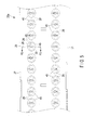
FIG. 4 illustrates a plan view of the light-emitting module integrated in the luminaire inFIG. 1 viewed from a side where light goes out; -
FIG. 5 illustrates a partly enlarged plan view of an area F5 inFIG. 4 in an enlarged scale; -
FIG. 6 illustrates a cross-sectional view taken along line F6-F6 inFIG. 5 ; -
FIG. 7 illustrates a plan view of a configuration inFIG. 6 when viewed in a direction of an arrow F7; -
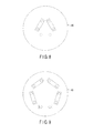
FIG. 8 illustrates a schematic drawing of a first modification in which a posture of LED chips inFIG. 7 is changed; -
FIG. 9 illustrates a schematic drawing of a second modification; -
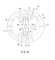
FIG. 10 illustrates a plan view of a principal portion of the light-emitting module according to a second embodiment; -
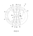
FIG. 11 illustrates a plan view of a modification of the light-emitting module inFIG. 10 ; -
FIG. 12A illustrates a plan view for explaining a method of optimizing a shape of a sealing member of the light-emitting module inFIG. 10 ; and -
FIG. 12B is a cross-sectional view ofFIG. 12A . - A light-emitting module according to an embodiment is configured by mounting a plurality of semiconductor light-emitting elements having the same light-emitting property on a substrate in a closed-up manner, and the plurality of closed-up semiconductor light-emitting elements are sealed altogether with a sealing member having a dome shape.
- Various Embodiments will be described hereinafter with reference to the accompanying drawings.
- Referring now to
FIG. 1 to FIG. 7 , a first embodiment will be described. -
FIG. 1 to FIG. 3 illustrate abase light 1 for general lighting. Thebase light 1 is an example of a luminaire used, for example, indoors, surface mounted to a ceiling surface C of a building. - The
base light 1 is provided with anapparatus body 2, a pair ofshades 3, alight source 4, and alighting circuit 5. Theapparatus body 2 has achassis 6, acenter cover 7, afirst side cover 8a, and asecond side cover 8b. - The
chassis 6 is formed of a plate material such as galvanized steel plate and has an elongated shape extending along the ceiling surface C. Thechassis 6 includes afixing portion 10, and a pair of lightsource supporting portions - The
fixing portion 10 has a substantially flat plate shape and is fixed, for example, to an element which constitutes a ceiling of a building with a plurality of screws. The lightsource supporting portions fixing portion 10 therebetween. The lightsource supporting portions surface 12. The supportingsurface 12 protrudes downward with respect to thefixing portion 10, and extends straight in the longitudinal direction of thechassis 6. - The
center cover 7 is mounted to thefixing portion 10 of thechassis 6. The center cover 7 projects into a V-shape downward of thechassis 6 from between the lightsource supporting portions - The
first side cover 8a covers one end along the longitudinal direction of thechassis 6 and one end along the longitudinal direction of thecenter cover 7 continuously. Thesecond side cover 8b covers the other end along the longitudinal direction of thechassis 6 and the other end along the longitudinal direction of thecenter cover 7 continuously. - The
shades 3 are formed of translucent resin material such as acryl resin or polycarbonate resin. Theshades 3 extend straight in the longitudinal direction of thechassis 6. - As illustrated in
FIG. 3 , theshades 3 have an opening 13 opening toward the lightsource supporting portions chassis 6. Theopening 13 has a slit-shape extending in the longitudinal direction of thechassis 6. A pair ofholding grooves opening 13. Theholding grooves shades 3. Opening ends of theholding grooves chassis 6. - In addition, the
shades 3 are mounted on thechassis 6 via a plurality of brackets. When theshades 3 are mounted on thechassis 6, the lightsource supporting portions chassis 6 are covered by theshades 3 from below. - As illustrated in
FIG. 2 , thelight source 4 includes a first to sixth light-emitting modules emitting modules source supporting portions - According to the first embodiment, the first to third light-
emitting modules holding grooves shades 3, and are arranged in a line so as to extend along the longitudinal direction of the lightsource supporting portion 11a. In the same manner, the fourth to sixth light-emitting modules holding grooves shades 3, and are arranged in a line so as to extend along the longitudinal direction of the lightsource supporting portion 11b. - Therefore, the first to sixth light-
emitting modules shades 3 and are covered with theshades 3. In addition, the first to sixth light-emitting modules - The
lighting circuit 5 is configured to control lighting of the first to sixth light-emitting modules emitting modules lighting circuit 5 is supported by thefixing portion 10 of thechassis 6 and is covered with thecenter cover 7. - The first to sixth light-emitting
modules module 20a is described as a representative example. - As illustrated in
FIG. 4 to FIG. 6 , the first light-emittingmodule 20a includes asubstrate 21. Thesubstrate 21 has a three-layer structure having a base 22, ametallic layer 23, and a resistlayer 24. Thethickest base 22 is formed of a synthetic resin such as epoxy resin or glass composite substrate, and has an elongated shape extending in the longitudinal direction of thechassis 6. - The
metallic layer 23 is formed of, for example, copper foil, and is laminated on aback surface 22a of thebase 22. The resistlayer 24 is formed of an insulating material such as synthetic resin, for example. The resistlayer 24 is laminated continuously on themetallic layer 23 and an outer peripheral portion of theback surface 22a of thebase 22. Themetallic layer 23 and the resistlayer 24 reinforce thesubstrate 21 in cooperation with each other in order to prevent warping of thesubstrate 21. - The
substrate 21 includes a pair ofside edges FIG. 3 . The side edges 21a and 21b of thesubstrate 21 are inserted into the holdinggrooves shade 3 from one end along the longitudinal direction of theshade 3. As a result of the insertion, thesubstrate 21 is held by theshade 3, and the resistlayer 24 of thesubstrate 21 comes into contact with the supportingsurface 12 of the lightsource supporting portion 11a. - As illustrated in
FIG. 5 to FIG. 7 , a plurality ofconductive patterns 26 and an insulatinglayer 27 are laminated on afront surface 22b (mounting surface) of thebase 22. Theconductive patterns 26 are arranged in two rows at a distance in the width direction of thesubstrate 21, and are apart from each other in the longitudinal direction of thesubstrate 21 in each row. - The
conductive patterns 26 each include a mountingpad 28, a firstpower distribution pad 29, and a secondpower distribution pad 30. The mountingpad 28 employs a three-layer structure including, for example, first to third metallic layers Cu, N, S laminated one on top of another. - Specifically, the first metallic layer Cu is formed by applying etching on copper foil laminated on the
front surface 22b of thebase 22. The second metallic layer N is laminated on the first metallic layer Cu. The second metallic layer N is formed by applying nickel plating on the first metallic layer Cu. The third metallic layer S is laminated on the second metallic layer N. The third metallic layer S is formed by applying silver plating on the second metallic layer N. The third metallic layer S forms a surface layer of the mountingpad 28. - Therefore, a surface of the mounting
pad 28 corresponds to a silver light-reflectingsurface 31. The total beam reflectance of the light-reflectingsurface 31 is preferably, for example, at least 90%. The mountingpad 28 functions as a light-reflecting layer. - As illustrated in
FIG. 7 , the mountingpad 28 in this embodiment has a substantially oval shape and has a longitudinal axis L1 extending in the direction in which theconductive patterns 26 are arranged. The mountingpad 28 includes an outerperipheral edge 33 curved into an arc shape and a pair ofdepressed portions depressed portions peripheral edge 33 of the mountingpad 28 in an arcuate shape toward a center O1 of the mountingpad 28 where the longitudinal axis L1 passes, and are arranged along the direction orthogonal to the longitudinal axis L1 of the mountingpad 28. - In other words, the
depressed portions pad 28 therebetween. Therefore, the mountingpad 28 has a form narrowed at acentral portion 28a including the center O1. - The first and second
power distribution pads pad 28, and have the same size. The first and secondpower distribution pads pad 28, and the surface layers thereof are formed of silver. - The first and second
power distribution pads front surface 22b of the base 22 so as to be accommodated in thedepressed portions pad 28. In other words, the first and secondpower distribution pads pad 28 with respect to the center O1 of the mountingpad 28, and are arranged symmetrically with each other with respect to the longitudinal axis L1. - In addition, the first and second
power distribution pads depressed portions pad 28, and are kept in a state of being electrically insulated from the mountingpad 28. In other words, thedepressed portions pad 28 are notched so as to avoid the first and secondpower distribution pads - As illustrated in
FIG. 6 , the insulatinglayer 27 is laminated on thefront surface 22b of thebase 22. The insulatinglayer 27 covers an area of thefront surface 22b of the base 22 other than the mountingpad 28, the firstpower distribution pad 29, and the secondpower distribution pad 30. Therefore, each of the surface layer of the mountingpad 28, a surface layer of the firstpower distribution pad 29, and a surface layer of the secondpower distribution pad 30 is not covered with the insulatinglayer 27 and are exposed out from thesubstrate 21. - Part of the insulating
layer 27 is filled in thedepressed portions pad 28, and is interposed between the mountingpad 28 and the firstpower distribution pad 29, and between the mountingpad 28 and the secondpower distribution pad 30. In addition, the insulatinglayer 27 protrudes in the thickness direction of thesubstrate 21 with respect to the surface layer of the mountingpad 28, the surface layer of the firstpower distribution pad 29, and the surface layer of the secondpower distribution pad 30. - According to the first embodiment, the insulating
layer 27 is formed of, for example, a white resin material having an electrical insulating property. Therefore, the insulatinglayer 27 also has a function as the light reflecting layer. - As illustrated in
FIG. 7 , first to third light-emitting diodes (LED) 36a, 36b, and 36c (hereinafter, referred to asLED chips surface 31 of the mountingpad 28. TheLED chips LED chips - Furthermore, the
LED chips first electrode 37 as an anode and asecond electrode 38 as a cathode. The first andsecond electrodes LED chips substrate 21. - The
LED chips surface 31 using a die-bonding material 39 having translucency. According to the first embodiment, theLED chips pad 28 at thecentral portion 28a of the mountingpad 28 and are arranged in a zigzag pattern with respect to the longitudinal axis L1. - Specifically, the first light-emitting
diode 36a and the third light-emittingdiode 36c are shifted toward the firstpower distribution pad 29 with respect to the longitudinal axis L1. The second light-emittingdiode 36b is shifted toward the secondpower distribution pad 30 with respect to the longitudinal axis L1. - Therefore, as illustrated by a double dashed chain line in
FIG. 7 , theLED chips pad 28 at thecentral portion 28a of the mountingpad 28. More specifically, the centers of therespective LED chips - The
first electrodes 37 of theLED chips power distribution pad 29 via afirst bonding wire 41 individually. In the same manner, thesecond electrodes 38 of theLED chips power distribution pad 30 via asecond bonding wire 42 individually. - Consequently, the
LED chips pad 28 constitute adiode group 43 connected in parallel to each other. The diode groups 43 on the mountingpad 28 are connected in series along the direction of arrangement of theconductive patterns 26 and constitute two rows of diode rows corresponding to theconductive patterns 26 on thesubstrate 21. - Furthermore, according to the first embodiment, the
diode groups 43 are grounded via thechassis 6 of theapparatus body 2. - As illustrated in
FIG. 4 to FIG. 7 , a plurality of sealingmembers 45 are formed on thesubstrate 21. The sealingmembers 45 are arranged in two rows at a distance in the width direction of thesubstrate 21 so as to correspond to theconductive patterns 26, and are apart from each other in the longitudinal direction of thesubstrate 21 in each row. - The sealing
members 45 seal thediode groups 43 bonded to the mountingpad 28 and the first andsecond bonding wires diode groups 43 on thesubstrate 21. The sealingmembers 45 consist primarily of a resin, and include a predetermined amount of phosphor particles and a predetermined amount of filler mixed in the resin. - As a resin contained in the sealing
member 45, a resin-based silicone resin or a hybrid-based silicone resin having translucency are preferably used, for example. The resin-based silicon resin and the hybrid-based silicone resin have a three-dimensionally bridged structure, and hence are harder than translucent silicone rubber. - In addition, the resin-based silicone resin provides lower performance to allow gas such as oxygen or moisture vapor than silicone oil or silicone rubber. In the case of the first embodiment, oxygen transmittance of the sealing
members 45 is 1200 cm3 (m2 · day · atm) or lower and moisture transmittance is 35g/m2 or lower. - By selecting the resin of this type, degrading of the mounting
pad 28 caused by transmittance of the gas in the atmosphere through the sealingmembers 45 is prevented and the light-reflecting property of the light-reflectingsurface 31 is desirably maintained. - The phosphor particles contained in the sealing
member 45 have a diameter D of 1 µm or larger, and are dispersed in the resin substantially uniformly. As the phosphor particles, yellow phosphor particles which are excited by the blue light emitted by the LED chips and emit yellow light are used. The yellow is a complementary color with respect to blue, and presents white color by being mixed with blue. - However, the phosphor particles to be mixed with the sealing
members 45 are not limited to the yellow phosphor particles. For example, in order to improve color rendering properties of the light emitted from the LED chips, red phosphor particles exited by blue light and emitting red light, or green phosphor particles emitting green light may be added to the resin. - The sealing
member 45 is swelled from the insulatinglayer 27 of thesubstrate 21 so as to integrally enclose the mountingpad 28, the first and secondpower distribution pads pad 28, thediode group 43 on the mountingpad 28, and the first andsecond bonding wires diode group 43 and the first and secondpower distribution pads - The sealing
member 45 is formed by dropping the resin in a liquid state before being hardened toward the mountingpad 28. When dropping the material of the sealingmember 45, a dispenser is preferably used. The material of the sealingmember 45 dropped toward the mountingpad 28 is hardened into a dome shape by being heated at a temperature of, for example, 150°C for 60 minutes. - According to the sealing
member 45 in the first embodiment, the resin as the principal component thereof has physicality which maintains a predetermined shape even in a state of not being hardened immediately after the resin is dropped toward the mountingpad 28. The physicality of the resin here means thixotropy or viscosity. - In other words, as illustrated in
FIG. 6 , the sealingmember 45 is configured to maintain the dome shape so as to continuously cover the mountingpad 28, the first and secondpower distribution pads diode group 43 and the first andsecond bonding wires pad 28. - As illustrated in
FIG. 5 andFIG. 7 in plan view, the dome shaped sealingmembers 45 have a substantially oval shape having commonly the longitudinal axis L1 of the mountingpads 28 and are arranged in the longitudinal direction of thesubstrate 21 at a distance. The shape of the sealingmember 45 is not limited to the oval shape and may be a circular shape etc. - With the
base light 1 configured as described above, when a power switch of thebase light 1 is turned ON, a DC voltage is applied from thelighting circuit 5 to theconductive patterns 26 of the first to sixth light-emittingmodules diode groups 43 mounted on the plurality of mountingpads 28 emit light altogether. - Blue light emitted from the bear chips of the
diode groups 43 enters the sealingmembers 45. Part of the blue light entering the sealingmembers 45 is absorbed by the phosphor particles. The remaining part of the blue light passes through the sealingmembers 45 without being absorbed by the phosphor particles. - The phosphor particles which absorbed the blue light are excited and emit yellow light which is a complementary color. The yellow light passes through the sealing
members 45. Therefore, the yellow light and the blue light are mixed to each other in the interior of the sealingmembers 45 and generate white light. The white light passes through the sealingmembers 45 and theshades 3 and is radiated out of thebase light 1, and is provided to light the room from the ceiling surface C. - In the first embodiment, the case where the LED chips emitting blue light has been described. However, for example, LED chips emitting ultraviolet rays may be employed. In this case, in order to cause the
diode groups 43 to emit white light, phosphor which absorbs the ultraviolet rays and excites and emits light having peaks of three wavelengths including blue, red, and green may be mixed into the sealingmembers 45. - Furthermore, according to the first embodiment, the mounting
pad 28 has thedepressed portions pad 28, and hence has a shape narrowed at thecentral portion 28a of the mountingpad 28. In contrast, the first and secondpower distribution pads second bonding wires pad 28, and the surface areas of the first and secondpower distribution pads - In this configuration, the surface areas of the first and second
power distribution pads pads 28 each having the light-reflectingsurface 31 on the surface thereof, and excessive electrical charge is prevented from accumulating between grounding portions of the first to sixth light-emittingmodules power distribution pads - Consequently, when the power switch of the
base light 1 is turned OFF and the first to sixth light-emittingmodules diode groups 43 of the first to sixth light-emittingmodules - Therefore, dark lightening of the
base light 1 which thediode groups 43 emit light weakly can be eliminated almost perfectly. - In particular, according to the first embodiment, as illustrated in
FIG. 7 , since the surface areas of the first and secondpower distribution pads bonding wires power distribution pads bonding wires - As described above, according to the first embodiment, the plurality of (three in the first embodiment)
LED chips substrate 21 in a closed-up manner, and the plurality ofLED chips member 45 together. Therefore, provision of a bank (frame) for pouring the resin material of the sealing members is not necessary, and the manufacturing cost of the light-emittingmodule 20a may be reduced correspondingly. Also, since the bank is not provided, the light emitted from the plurality ofLED chips module 20a having a desirable appearance is provided. - According to the first embodiment, the plurality of
LED chips member 45, light-emission intensity as thediode groups 43 may be enhanced, the luminous flux of the light-emittingmodule 20a may be increased, and the light-emission intensity of thebase light 1 may be enhanced. In other words, in comparison with the luminaire of the related art in which one LED chip is sealed by one sealing member, the luminous flux emitted from thediode groups 43 may be increased to substantially three times, and the light-emission intensity may be enhanced correspondingly. Consequently, the number of light-emittingmodules 20a may be reduced and, in addition, the number of base lights 1 (luminaires) may also be reduced, so that energy saving is achieved. - Since the plurality of
LED chips member 45, the light-emitting efficiency of the light-emittingmodule 20a may be enhanced. For example, a light emitting element, configured to emit light of 100 lm when a current of 100 mA is passed through a single LED chip, has a feature such that the rate of the current converted to heat at the time of light emission is reduced when a current of 50 mA, which is a half, is passed therethrough. Therefore, for example, the light-emitting element emits light of 55 lm, which exceeds 50 lm. Therefore, when considering thediode groups 43, the efficiency of energy conversion may be enhanced by reducing the current to be passed through the one LED chip, and the light-emitting efficiency of the light-emittingmodule 20a as a whole is enhanced. - According to the first embodiment, since the plurality of
LED chips member 45, variability of the light-emitting properties from one LED chip to another is reduced. In other words, when the one LED chip is sealed by one sealing member, the variability of light-emitting properties from one LED chip to another directly leads to the variability of light-emitting properties of the sealed light-emitting elements. However, by sealing the plurality ofLED chips member 45 together as in the first embodiment, the variability of the light-emitting properties of the respective chips are compensated, and the variability of light emitting properties of the light-emitting module as a whole is reduced. - In the first embodiment described above, the configuration in which the three
LED chips member 45 has been described. However, the number of LED chips to be sealed altogether by the sealingmember 45 only has to be plural, and the effect as described above is achieved as long as two or more LED chips are provided. In other words, the number of LED chips may be at least two or more, for example, four or more. - In contrast, when the number of the LED chips to be sealed by the one sealing
member 45 increases, the required amount of the sealing members increases inevitably, and the surface area of a sealed area also increases. Therefore, it is expected that maintaining the dome shape of the sealingmember 45 becomes difficult, and hence the light-emitting property is affected. In other words, when a larger number of the LED chips are sealed in the sealingmember 45 having a largest diameter which can maintain the dome shape, the distance between the LED chip and a surface of the sealingmember 45 is gradually reduced. In such a case, an optical path length of light emitted from the LED chip and going out from the surface of the sealingmember 45 is reduced, and the ratio of blue light which is radiated as-is without being absorbed by the phosphor particles is increased, and hence color variability may occur. - Therefore, in the first embodiment, in order to prevent the above-described color variability, the plurality of
LED chips member 45 in a closed-up state. In order to measure the density which does not cause the color variability, an adequate range of a mounting area for mounting the LED chips which does not cause the color variability was inspected by changing variously the ratio of the diameter of the mounting area with respect to the diameter of the sealed area sealed by the sealingmember 45. Consequently, in the case of the light-emittingmodule 20a having a layout in which the LED chips are arranged at the apexes of a regular polygon as in the first embodiment, a case in which the diameter of the mounting area for mounting the LED chips is set to 1/2 or smaller of the diameter of the sealed area sealed by the sealingmember 45 was found to be best to obtain a desirable light-emitting property without causing any color variability. - In the first embodiment described above, the layout in which the
LED chips - When the size of the LED chips may be reduced, and the diameter of the sealed area sealed by the sealing
member 45 which can maintain the dome shape can be increased, the plurality of LED chips may be arranged in double or triple ring shapes. In such a case, color difference of light emitted from the respective LED chips depending on the angles may be eliminated, and further desirable light-emitting property is obtained. - Furthermore, by employing the layout in which the plurality of LED chips are arranged in a regular polygonal shape and devising a mounting posture of the respective LED chips themselves, occurrence of the color variability as the
diode group 43 can be prevented further reliably. In other words, for example, by arranging all the LED chips in the postures in which longitudinal axes of the respective chips extend along the respective sides of the regular polygon as in the modification exemplified inFIG. 8 or FIG. 9 , a layout of point symmetry with respect to the center of the sealingmember 45 is achieved, and the distances from light-emitting portions of the respective LED chips to an edge of the sealingmember 45 may be substantially equalized, and hence the occurrence of the color variability is substantially eliminated. - The shape of the sealing
member 45 in the modifications illustrated inFIG. 8 and FIG. 9 is preferably circular in comparison with the oval shape. In this case, although not illustrated, power distribution pads configured to distribute power to the respective LED chips are needed to be provided one for each LED, and are required to be arranged within the sealed area and outside the mounting area for mounting the LED chips. For Example, in the case of the modification inFIG. 9 , ten of the power distribution pads need to be prepared for distributing power to the five LED chips respectively, and are arranged in a ring shape on the outside of the mounting area. - In other words, according to the two modifications described above, the respective power distribution pads may be divided into small pieces to reduce the surface area and hence the problem of the dark lighting described above is further reduced.
-
FIG. 10 illustrates a plan view of a principal portion of a light-emittingmodule 50 according to a second embodiment. The light-emittingmodule 50 according to the second embodiment has the substantially same structure as the light-emittingmodule 20a according to the first embodiment described above except that the layout of theLED chips module 20a of the first embodiment are designated by the same reference signs, and the detailed description is omitted. - A
diode group 52 of the light-emittingmodule 50 according to the second embodiment includes a chip layout in which the plurality of (three in the second embodiment)LED chips LED chips member 45 and the longitudinal axes of therespective LED chips - According to the second embodiment, the same effect as the first embodiment described above is achieved. Furthermore, according to the second embodiment, since the plurality of LED chips are arranged in a line, the layout of the chips is easier and the wire bonding is also easier, and the manufacture of the light-emitting
module 50 is easier than the first embodiment described above, and reduction of the manufacturing cost of the light-emittingmodule 50 is achieved. - In the second embodiment as well, when the optimal diameter of the mounting area for mounting the LED chips which does not cause the color variation was inspected, the desirable light-emitting property without any color variability was found to be obtained when all the LED chips are mounted within a range of a diameter of 2/3 or smaller of the diameter of the sealed area.
- To name a detailed example, when the length along the longitudinal axis of the LED chip is 0.6 mm, the width is 0.2 mm and the diameter of the sealing
member 45 is 6 mm, the optimal diameter of the mounting area for mounting the LED chips falls within the above-described range by setting the width of the area in which the three LED chips are arranged and mounted side by side to 4 mm or smaller. In other words, in this case, the diameter of the mounting area for mounting the LED chips can be set to 2/3 or smaller of the diameter of the sealed area sealed by the sealingmember 45, so that the color variability is prevented. - In the second embodiment, the case where the three
LED chips bonding wires power distribution pads - Therefore, as in the modification illustrated in
FIG. 11 , a method of preparing individualpower distribution pads respective LED chips - By employing the method described above, as illustrated in the drawing, the
bonding wires power distribution pads - In such a case, in comparison with the second embodiment described above, since the number of
bonding wires - However, in the second embodiment, if the number of LED chips is increased, the shape of the sealing
member 45 is changed from the circular shape to the elongated oval shape, and the range of the optimal mounting area can hardly be specified with the comparison with the diameters as described above. Therefore, in the case of the second embodiment, the color variability is eliminated by setting a proper distance between the respective LED chips and the surface of the sealingmember 45 instead of specifying the range of the mounting area. -
FIG. 12A and FIG. 12B illustrate an optimal shape of the sealingmember 45 when the threeLED chips FIG. 12A , the shape of aperipheral edge 45a of the optimal sealingmember 45 is an oval shape, and the distances D from therespective LED chips peripheral edge 45a are all the same. As illustrated in a cross-sectional view inFIG. 12B , distances D from the upper surface of therespective LED chips top portion 45b of the sealingmember 45 are also the same. - In other words, light emitted from the
respective LED chips member 45, and emits yellow light. However, the amount of the yellow light is determined according to the optical path length of light emitted from therespective LED chips member 45. The amount of blue light transmitted is also determined according to the optical path length. In other words, by equalizing all the distances D from therespective LED chips member 45, the color variability is also prevented. - According to the light-emitting module and the luminaire of at least one of embodiment described above, since the plurality of LED chips are sealed by the sealing member in a closed-up manner, the light-emitting surface area may be increased, and the sufficiently satisfactory luminous flux may be obtained, and the energy efficiency may be enhanced.
- For example, in the embodiments described above, a base light which is to be surface mounted to the ceiling has been described as the luminaire. However, the luminaire is not limited thereto, and may also be implemented in luminaires of other forms such as street lights or guide lights.
- While certain embodiments have been described, these embodiments have been presented by way of example only, and are not intended to limit the scope of the inventions. Indeed, the novel embodiments described herein may be embodied in a variety of other forms; furthermore, various omissions, substitutions and changes in the form of the embodiments described herein may be made without departing from the spirit of the inventions. The accompanying claims and their equivalents are intended to cover such forms or modifications as would fall within the scope and spirit of the inventions.
Claims (10)
- A light-emitting module characterized by comprising:a plurality of light-emitting elements (36a, 36b, 36c) having the same light-emitting property;a substrate (21) on which the plurality of light-emitting elements are mounted in a closed up manner; anda sealing member (45) having a dome shape configured to seal the plurality of light-emitting elements mounted on the substrate altogether.
- The light-emitting module according to claim 1, characterized in that
the plurality of light-emitting elements (36a, 36b, 36c) sealed by the sealing member (45) are arranged in a line in proximity to each other. - The light-emitting module according to claim 2, characterized in that
the plurality of light-emitting elements (36a, 36b, 36c) arranged in a line are arranged within a mounting area having a diameter of 2/3 or smaller of the diameter of a sealed area of the sealing member (45). - The light-emitting module according to claim 2 or 3, characterized in that
the plurality of light-emitting elements (36a, 36b, 36c) arranged in a line are sealed by the sealing member (45) having an oval shape or an ellipse shape having a longitudinal axis along the direction of arrangement thereof. - The light-emitting module according to claim 1, characterized in that
the plurality of light-emitting elements (36a, 36b, 36c) sealed by the sealing member (45) are arranged in a ring shape. - The light-emitting module according to claim 5, characterized in that
the plurality of light-emitting elements (36a, 36b, 36c) arranged in the ring shape are arranged within the mounting area having a diameter of 1/2 or smaller of the diameter of the sealed area of the sealing member (45). - The light-emitting module according to claim 1, characterized by further comprising:a light reflecting layer (28) provided on a mounting surface (22b) of the substrate (21); andpower distribution pads (29, 30) provided on the mounting surface separately from the light reflecting layer and having a surface area smaller than that of the light reflecting layer.
- The light-emitting module according to claim 7, characterized in that
bonding wires (41, 42) configured to connect the respective light-emitting elements (36a, 36b, 36c) and the power distribution pads (29, 30) converge on the power distribution pads. - The light-emitting module according to claim 7, characterized in that
the power distribution pads (29, 30) are divided into a plurality of portions (29a, 29b, 29c, 30a, 30b, 30c) configured to distribute power to the plurality of light-emitting elements (36a, 36b, 36c) sealed by the sealing member (45) respectively and individually, and
the bonding wires (41, 42) connecting the respective light-emitting elements and the plurality of portions of the power distribution pads spread to the plurality of portions. - A luminaire characterized by comprising:a main body (2) including a supporting surface (12);light-emitting modules (20a, 20b, 20c, 20d, 20e, 20f) according to any one of claims 1 to 9 provided so as to come into contact with the supporting surface;
anda lighting circuit (5) configured to light the light-emitting module.
Applications Claiming Priority (1)
| Application Number | Priority Date | Filing Date | Title |
|---|---|---|---|
| JP2011241236A JP2013098416A (en) | 2011-11-02 | 2011-11-02 | Light emitting module and lighting device |
Publications (2)
| Publication Number | Publication Date |
|---|---|
| EP2590214A2 true EP2590214A2 (en) | 2013-05-08 |
| EP2590214A3 EP2590214A3 (en) | 2015-03-04 |
Family
ID=46851817
Family Applications (1)
| Application Number | Title | Priority Date | Filing Date |
|---|---|---|---|
| EP12181464.4A Withdrawn EP2590214A3 (en) | 2011-11-02 | 2012-08-23 | Light-emitting module and luminaire |
Country Status (4)
| Country | Link |
|---|---|
| US (1) | US8766536B2 (en) |
| EP (1) | EP2590214A3 (en) |
| JP (1) | JP2013098416A (en) |
| CN (1) | CN103094265A (en) |
Families Citing this family (8)
| Publication number | Priority date | Publication date | Assignee | Title |
|---|---|---|---|---|
| JP2015061024A (en) * | 2013-09-20 | 2015-03-30 | パナソニック株式会社 | Light emitting module |
| JP6497615B2 (en) * | 2015-03-04 | 2019-04-10 | パナソニックIpマネジメント株式会社 | Mounting board and LED module using the same |
| JP2016162971A (en) * | 2015-03-04 | 2016-09-05 | パナソニックIpマネジメント株式会社 | LED module |
| JP6685738B2 (en) * | 2016-01-25 | 2020-04-22 | コーデンシ株式会社 | Light emitting device |
| JP6645486B2 (en) * | 2017-02-13 | 2020-02-14 | 日亜化学工業株式会社 | Light emitting device and method of manufacturing the same |
| JP6955407B2 (en) * | 2017-09-13 | 2021-10-27 | 日本特殊陶業株式会社 | Holding device |
| CN109031779B (en) * | 2018-07-25 | 2024-06-11 | 京东方科技集团股份有限公司 | Light-emitting diode substrate, backlight module and display device |
| KR102664521B1 (en) * | 2022-07-29 | 2024-05-09 | 엘지전자 주식회사 | Semiconductor light-emitting device package and display device |
Family Cites Families (13)
| Publication number | Priority date | Publication date | Assignee | Title |
|---|---|---|---|---|
| JP3420612B2 (en) * | 1993-06-25 | 2003-06-30 | 株式会社東芝 | LED lamp |
| JP2006332234A (en) * | 2005-05-25 | 2006-12-07 | Hitachi Aic Inc | LED device having reflection function |
| JP4880928B2 (en) * | 2005-07-01 | 2012-02-22 | 日本特殊陶業株式会社 | Wiring board |
| US7842960B2 (en) * | 2006-09-06 | 2010-11-30 | Lumination Llc | Light emitting packages and methods of making same |
| JP5432478B2 (en) * | 2007-07-26 | 2014-03-05 | パナソニック株式会社 | LED lighting device |
| JP5270991B2 (en) * | 2008-07-23 | 2013-08-21 | パナソニック株式会社 | Light emitting device and lighting apparatus |
| GB2458972B (en) * | 2008-08-05 | 2010-09-01 | Photonstar Led Ltd | Thermally optimised led chip-on-board module |
| JP5726409B2 (en) * | 2009-07-01 | 2015-06-03 | シャープ株式会社 | Light emitting device and method for manufacturing light emitting device |
| JP2011023138A (en) | 2009-07-13 | 2011-02-03 | Sharp Corp | Lighting system |
| US8455910B2 (en) * | 2009-09-21 | 2013-06-04 | Walsin Lihwa Corporation | Method of manufacturing light emitting diode packaging lens and light emitting diode package |
| JP4932064B2 (en) * | 2010-03-11 | 2012-05-16 | パナソニック株式会社 | Light emitting module, light source device, liquid crystal display device, and method for manufacturing light emitting module |
| JP5988073B2 (en) * | 2011-11-01 | 2016-09-07 | 東芝ライテック株式会社 | Light emitting module and lighting device |
| US20130169144A1 (en) * | 2012-01-03 | 2013-07-04 | Lustrous Technology Ltd. | Led package structure capable of adjusting the spatial color uniformity and the light distribution curve |
-
2011
- 2011-11-02 JP JP2011241236A patent/JP2013098416A/en active Pending
-
2012
- 2012-08-22 US US13/591,617 patent/US8766536B2/en not_active Expired - Fee Related
- 2012-08-23 EP EP12181464.4A patent/EP2590214A3/en not_active Withdrawn
- 2012-09-20 CN CN2012103532805A patent/CN103094265A/en active Pending
Non-Patent Citations (1)
| Title |
|---|
| None |
Also Published As
| Publication number | Publication date |
|---|---|
| EP2590214A3 (en) | 2015-03-04 |
| CN103094265A (en) | 2013-05-08 |
| US8766536B2 (en) | 2014-07-01 |
| JP2013098416A (en) | 2013-05-20 |
| US20130106279A1 (en) | 2013-05-02 |
Similar Documents
| Publication | Publication Date | Title |
|---|---|---|
| US8766536B2 (en) | Light-emitting module having light-emitting elements sealed with sealing member and luminaire having same | |
| JP5197874B2 (en) | Light emitting module, light source device, liquid crystal display device, and method for manufacturing light emitting module | |
| US9488345B2 (en) | Light emitting device, illumination apparatus including the same, and mounting substrate | |
| JP5291268B1 (en) | LIGHT EMITTING MODULE AND LIGHTING LIGHT SOURCE AND LIGHTING DEVICE USING THE SAME | |
| JP6440060B2 (en) | LIGHT EMITTING DEVICE AND LIGHTING DEVICE USING THE SAME | |
| EP2672513B1 (en) | Multichip package structure for generating a symmetrical and uniform light-blending source | |
| EP2397749A2 (en) | Light-emitting device and lighting apparatus | |
| US20110309379A1 (en) | Light-emitting device and luminare | |
| CN103890488B (en) | Light emitting module | |
| JP2015198252A (en) | Led assembly and led bulb using led assembly | |
| JP2016167518A (en) | Light emitting device and lighting device | |
| JP2014165190A (en) | Laminate body of light emitting device | |
| JP2010251796A (en) | Light emitting module | |
| JP5656051B2 (en) | Light emitting device and lighting device | |
| JP2014026995A (en) | Light-emitting device and luminaire | |
| JP5212178B2 (en) | Light emitting module | |
| JP2017112288A (en) | Light-emitting device | |
| JP2014175393A (en) | Light-emitting device | |
| EP2590237A2 (en) | Light-emitting module and illumination device | |
| CN204088375U (en) | Led module and lighting device |
Legal Events
| Date | Code | Title | Description |
|---|---|---|---|
| PUAI | Public reference made under article 153(3) epc to a published international application that has entered the european phase |
Free format text: ORIGINAL CODE: 0009012 |
|
| AK | Designated contracting states |
Kind code of ref document: A2 Designated state(s): AL AT BE BG CH CY CZ DE DK EE ES FI FR GB GR HR HU IE IS IT LI LT LU LV MC MK MT NL NO PL PT RO RS SE SI SK SM TR |
|
| AX | Request for extension of the european patent |
Extension state: BA ME |
|
| PUAL | Search report despatched |
Free format text: ORIGINAL CODE: 0009013 |
|
| AK | Designated contracting states |
Kind code of ref document: A3 Designated state(s): AL AT BE BG CH CY CZ DE DK EE ES FI FR GB GR HR HU IE IS IT LI LT LU LV MC MK MT NL NO PL PT RO RS SE SI SK SM TR |
|
| AX | Request for extension of the european patent |
Extension state: BA ME |
|
| RIC1 | Information provided on ipc code assigned before grant |
Ipc: H01L 25/075 20060101AFI20150123BHEP |
|
| STAA | Information on the status of an ep patent application or granted ep patent |
Free format text: STATUS: THE APPLICATION IS DEEMED TO BE WITHDRAWN |
|
| 18D | Application deemed to be withdrawn |
Effective date: 20150905 |