EP2587541A1 - Light emitting device - Google Patents
Light emitting device Download PDFInfo
- Publication number
- EP2587541A1 EP2587541A1 EP20120190187 EP12190187A EP2587541A1 EP 2587541 A1 EP2587541 A1 EP 2587541A1 EP 20120190187 EP20120190187 EP 20120190187 EP 12190187 A EP12190187 A EP 12190187A EP 2587541 A1 EP2587541 A1 EP 2587541A1
- Authority
- EP
- European Patent Office
- Prior art keywords
- light emitting
- semiconductor layer
- layer
- disposed
- emitting regions
- Prior art date
- Legal status (The legal status is an assumption and is not a legal conclusion. Google has not performed a legal analysis and makes no representation as to the accuracy of the status listed.)
- Granted
Links
- 239000004065 semiconductor Substances 0.000 claims abstract description 203
- 229910052751 metal Inorganic materials 0.000 claims description 34
- 239000002184 metal Substances 0.000 claims description 34
- 238000002161 passivation Methods 0.000 claims description 24
- 239000000758 substrate Substances 0.000 claims description 23
- 239000010410 layer Substances 0.000 description 386
- 230000004888 barrier function Effects 0.000 description 15
- 239000000463 material Substances 0.000 description 15
- XLOMVQKBTHCTTD-UHFFFAOYSA-N Zinc monoxide Chemical compound [Zn]=O XLOMVQKBTHCTTD-UHFFFAOYSA-N 0.000 description 12
- 230000000903 blocking effect Effects 0.000 description 11
- PXHVJJICTQNCMI-UHFFFAOYSA-N nickel Substances [Ni] PXHVJJICTQNCMI-UHFFFAOYSA-N 0.000 description 11
- 230000003287 optical effect Effects 0.000 description 9
- 150000001875 compounds Chemical class 0.000 description 8
- 238000009792 diffusion process Methods 0.000 description 8
- 238000005530 etching Methods 0.000 description 8
- VYPSYNLAJGMNEJ-UHFFFAOYSA-N Silicium dioxide Chemical compound O=[Si]=O VYPSYNLAJGMNEJ-UHFFFAOYSA-N 0.000 description 7
- 229910052759 nickel Inorganic materials 0.000 description 7
- 238000000605 extraction Methods 0.000 description 6
- 239000010931 gold Substances 0.000 description 6
- 229910052738 indium Inorganic materials 0.000 description 6
- 239000011787 zinc oxide Substances 0.000 description 6
- -1 aluminum tin oxide Chemical compound 0.000 description 5
- JAONJTDQXUSBGG-UHFFFAOYSA-N dialuminum;dizinc;oxygen(2-) Chemical compound [O-2].[O-2].[O-2].[O-2].[O-2].[Al+3].[Al+3].[Zn+2].[Zn+2] JAONJTDQXUSBGG-UHFFFAOYSA-N 0.000 description 5
- 239000011241 protective layer Substances 0.000 description 5
- 229910052710 silicon Inorganic materials 0.000 description 5
- JMASRVWKEDWRBT-UHFFFAOYSA-N Gallium nitride Chemical compound [Ga]#N JMASRVWKEDWRBT-UHFFFAOYSA-N 0.000 description 4
- GWEVSGVZZGPLCZ-UHFFFAOYSA-N Titan oxide Chemical compound O=[Ti]=O GWEVSGVZZGPLCZ-UHFFFAOYSA-N 0.000 description 4
- PNEYBMLMFCGWSK-UHFFFAOYSA-N aluminium oxide Inorganic materials [O-2].[O-2].[O-2].[Al+3].[Al+3] PNEYBMLMFCGWSK-UHFFFAOYSA-N 0.000 description 4
- 229910052593 corundum Inorganic materials 0.000 description 4
- 238000010586 diagram Methods 0.000 description 4
- 239000002019 doping agent Substances 0.000 description 4
- 229910052737 gold Inorganic materials 0.000 description 4
- 230000017525 heat dissipation Effects 0.000 description 4
- APFVFJFRJDLVQX-UHFFFAOYSA-N indium atom Chemical compound [In] APFVFJFRJDLVQX-UHFFFAOYSA-N 0.000 description 4
- 238000000034 method Methods 0.000 description 4
- 239000011347 resin Substances 0.000 description 4
- 229920005989 resin Polymers 0.000 description 4
- 229910052709 silver Inorganic materials 0.000 description 4
- 239000002356 single layer Substances 0.000 description 4
- 229910001887 tin oxide Inorganic materials 0.000 description 4
- 229910001845 yogo sapphire Inorganic materials 0.000 description 4
- 229910002704 AlGaN Inorganic materials 0.000 description 3
- 229910002601 GaN Inorganic materials 0.000 description 3
- GYHNNYVSQQEPJS-UHFFFAOYSA-N Gallium Chemical compound [Ga] GYHNNYVSQQEPJS-UHFFFAOYSA-N 0.000 description 3
- 229910001218 Gallium arsenide Inorganic materials 0.000 description 3
- 229910052581 Si3N4 Inorganic materials 0.000 description 3
- XUIMIQQOPSSXEZ-UHFFFAOYSA-N Silicon Chemical compound [Si] XUIMIQQOPSSXEZ-UHFFFAOYSA-N 0.000 description 3
- 229910052681 coesite Inorganic materials 0.000 description 3
- 239000010949 copper Substances 0.000 description 3
- 229910052906 cristobalite Inorganic materials 0.000 description 3
- 239000007772 electrode material Substances 0.000 description 3
- 229910052733 gallium Inorganic materials 0.000 description 3
- 239000011810 insulating material Substances 0.000 description 3
- VRIVJOXICYMTAG-IYEMJOQQSA-L iron(ii) gluconate Chemical compound [Fe+2].OC[C@@H](O)[C@@H](O)[C@H](O)[C@@H](O)C([O-])=O.OC[C@@H](O)[C@@H](O)[C@H](O)[C@@H](O)C([O-])=O VRIVJOXICYMTAG-IYEMJOQQSA-L 0.000 description 3
- 239000007769 metal material Substances 0.000 description 3
- 238000012986 modification Methods 0.000 description 3
- 230000004048 modification Effects 0.000 description 3
- 229910052697 platinum Inorganic materials 0.000 description 3
- 239000010703 silicon Substances 0.000 description 3
- HBMJWWWQQXIZIP-UHFFFAOYSA-N silicon carbide Chemical compound [Si+]#[C-] HBMJWWWQQXIZIP-UHFFFAOYSA-N 0.000 description 3
- 239000000377 silicon dioxide Substances 0.000 description 3
- 229910052682 stishovite Inorganic materials 0.000 description 3
- 239000011135 tin Substances 0.000 description 3
- 238000002834 transmittance Methods 0.000 description 3
- 229910052905 tridymite Inorganic materials 0.000 description 3
- 229910052725 zinc Inorganic materials 0.000 description 3
- 239000011701 zinc Substances 0.000 description 3
- 239000004698 Polyethylene Substances 0.000 description 2
- 229910019897 RuOx Inorganic materials 0.000 description 2
- DZLPZFLXRVRDAE-UHFFFAOYSA-N [O--].[O--].[O--].[O--].[Al+3].[Zn++].[In+3] Chemical compound [O--].[O--].[O--].[O--].[Al+3].[Zn++].[In+3] DZLPZFLXRVRDAE-UHFFFAOYSA-N 0.000 description 2
- 239000003795 chemical substances by application Substances 0.000 description 2
- 239000011248 coating agent Substances 0.000 description 2
- 238000000576 coating method Methods 0.000 description 2
- 239000004020 conductor Substances 0.000 description 2
- 229910052802 copper Inorganic materials 0.000 description 2
- PMHQVHHXPFUNSP-UHFFFAOYSA-M copper(1+);methylsulfanylmethane;bromide Chemical compound Br[Cu].CSC PMHQVHHXPFUNSP-UHFFFAOYSA-M 0.000 description 2
- 230000003247 decreasing effect Effects 0.000 description 2
- YZZNJYQZJKSEER-UHFFFAOYSA-N gallium tin Chemical compound [Ga].[Sn] YZZNJYQZJKSEER-UHFFFAOYSA-N 0.000 description 2
- 229910052732 germanium Inorganic materials 0.000 description 2
- HRHKULZDDYWVBE-UHFFFAOYSA-N indium;oxozinc;tin Chemical compound [In].[Sn].[Zn]=O HRHKULZDDYWVBE-UHFFFAOYSA-N 0.000 description 2
- 239000004973 liquid crystal related substance Substances 0.000 description 2
- 229910052750 molybdenum Inorganic materials 0.000 description 2
- 229910052763 palladium Inorganic materials 0.000 description 2
- BASFCYQUMIYNBI-UHFFFAOYSA-N platinum Substances [Pt] BASFCYQUMIYNBI-UHFFFAOYSA-N 0.000 description 2
- 229920003229 poly(methyl methacrylate) Polymers 0.000 description 2
- 229920000515 polycarbonate Polymers 0.000 description 2
- 239000004417 polycarbonate Substances 0.000 description 2
- 229920000573 polyethylene Polymers 0.000 description 2
- 229920000139 polyethylene terephthalate Polymers 0.000 description 2
- 239000005020 polyethylene terephthalate Substances 0.000 description 2
- 229920000642 polymer Polymers 0.000 description 2
- 239000004926 polymethyl methacrylate Substances 0.000 description 2
- 238000002310 reflectometry Methods 0.000 description 2
- 229910052594 sapphire Inorganic materials 0.000 description 2
- 239000010980 sapphire Substances 0.000 description 2
- 229910010271 silicon carbide Inorganic materials 0.000 description 2
- 229910052814 silicon oxide Inorganic materials 0.000 description 2
- 239000010944 silver (metal) Substances 0.000 description 2
- 239000000126 substance Substances 0.000 description 2
- 229910052718 tin Inorganic materials 0.000 description 2
- XOLBLPGZBRYERU-UHFFFAOYSA-N tin dioxide Chemical compound O=[Sn]=O XOLBLPGZBRYERU-UHFFFAOYSA-N 0.000 description 2
- 229910052719 titanium Inorganic materials 0.000 description 2
- YVTHLONGBIQYBO-UHFFFAOYSA-N zinc indium(3+) oxygen(2-) Chemical compound [O--].[Zn++].[In+3] YVTHLONGBIQYBO-UHFFFAOYSA-N 0.000 description 2
- 229910000980 Aluminium gallium arsenide Inorganic materials 0.000 description 1
- PIGFYZPCRLYGLF-UHFFFAOYSA-N Aluminum nitride Chemical compound [Al]#N PIGFYZPCRLYGLF-UHFFFAOYSA-N 0.000 description 1
- JBRZTFJDHDCESZ-UHFFFAOYSA-N AsGa Chemical compound [As]#[Ga] JBRZTFJDHDCESZ-UHFFFAOYSA-N 0.000 description 1
- RYGMFSIKBFXOCR-UHFFFAOYSA-N Copper Chemical compound [Cu] RYGMFSIKBFXOCR-UHFFFAOYSA-N 0.000 description 1
- 239000004593 Epoxy Substances 0.000 description 1
- 229910005540 GaP Inorganic materials 0.000 description 1
- ZOKXTWBITQBERF-UHFFFAOYSA-N Molybdenum Chemical compound [Mo] ZOKXTWBITQBERF-UHFFFAOYSA-N 0.000 description 1
- 229910020286 SiOxNy Inorganic materials 0.000 description 1
- 229910000577 Silicon-germanium Inorganic materials 0.000 description 1
- 229910045601 alloy Inorganic materials 0.000 description 1
- 239000000956 alloy Substances 0.000 description 1
- 229910052782 aluminium Inorganic materials 0.000 description 1
- 230000003667 anti-reflective effect Effects 0.000 description 1
- 238000005229 chemical vapour deposition Methods 0.000 description 1
- 229910052804 chromium Inorganic materials 0.000 description 1
- 239000002131 composite material Substances 0.000 description 1
- 239000000470 constituent Substances 0.000 description 1
- SBYXRAKIOMOBFF-UHFFFAOYSA-N copper tungsten Chemical compound [Cu].[W] SBYXRAKIOMOBFF-UHFFFAOYSA-N 0.000 description 1
- 238000000151 deposition Methods 0.000 description 1
- 230000008021 deposition Effects 0.000 description 1
- 230000006866 deterioration Effects 0.000 description 1
- PCHJSUWPFVWCPO-UHFFFAOYSA-N gold Chemical compound [Au] PCHJSUWPFVWCPO-UHFFFAOYSA-N 0.000 description 1
- 229910052735 hafnium Inorganic materials 0.000 description 1
- AMGQUBHHOARCQH-UHFFFAOYSA-N indium;oxotin Chemical compound [In].[Sn]=O AMGQUBHHOARCQH-UHFFFAOYSA-N 0.000 description 1
- 238000009413 insulation Methods 0.000 description 1
- 229910052741 iridium Inorganic materials 0.000 description 1
- 229910052742 iron Inorganic materials 0.000 description 1
- 238000002955 isolation Methods 0.000 description 1
- 238000004519 manufacturing process Methods 0.000 description 1
- QSHDDOUJBYECFT-UHFFFAOYSA-N mercury Chemical compound [Hg] QSHDDOUJBYECFT-UHFFFAOYSA-N 0.000 description 1
- 229910052753 mercury Inorganic materials 0.000 description 1
- 229910021645 metal ion Inorganic materials 0.000 description 1
- 239000011733 molybdenum Substances 0.000 description 1
- 229910052758 niobium Inorganic materials 0.000 description 1
- 239000010955 niobium Substances 0.000 description 1
- 150000004767 nitrides Chemical class 0.000 description 1
- 238000012536 packaging technology Methods 0.000 description 1
- 239000004038 photonic crystal Substances 0.000 description 1
- 238000007747 plating Methods 0.000 description 1
- 229920000728 polyester Polymers 0.000 description 1
- 239000002952 polymeric resin Substances 0.000 description 1
- 239000002096 quantum dot Substances 0.000 description 1
- 230000006798 recombination Effects 0.000 description 1
- 238000005215 recombination Methods 0.000 description 1
- SKRWFPLZQAAQSU-UHFFFAOYSA-N stibanylidynetin;hydrate Chemical compound O.[Sn].[Sb] SKRWFPLZQAAQSU-UHFFFAOYSA-N 0.000 description 1
- 229920003002 synthetic resin Polymers 0.000 description 1
- 229910052721 tungsten Inorganic materials 0.000 description 1
- 229910052720 vanadium Inorganic materials 0.000 description 1
Images


Classifications
-
- H—ELECTRICITY
- H01—ELECTRIC ELEMENTS
- H01L—SEMICONDUCTOR DEVICES NOT COVERED BY CLASS H10
- H01L27/00—Devices consisting of a plurality of semiconductor or other solid-state components formed in or on a common substrate
- H01L27/15—Devices consisting of a plurality of semiconductor or other solid-state components formed in or on a common substrate including semiconductor components with at least one potential-jump barrier or surface barrier specially adapted for light emission
- H01L27/153—Devices consisting of a plurality of semiconductor or other solid-state components formed in or on a common substrate including semiconductor components with at least one potential-jump barrier or surface barrier specially adapted for light emission in a repetitive configuration, e.g. LED bars
- H01L27/156—Devices consisting of a plurality of semiconductor or other solid-state components formed in or on a common substrate including semiconductor components with at least one potential-jump barrier or surface barrier specially adapted for light emission in a repetitive configuration, e.g. LED bars two-dimensional arrays
-
- H—ELECTRICITY
- H01—ELECTRIC ELEMENTS
- H01L—SEMICONDUCTOR DEVICES NOT COVERED BY CLASS H10
- H01L33/00—Semiconductor devices with at least one potential-jump barrier or surface barrier specially adapted for light emission; Processes or apparatus specially adapted for the manufacture or treatment thereof or of parts thereof; Details thereof
- H01L33/36—Semiconductor devices with at least one potential-jump barrier or surface barrier specially adapted for light emission; Processes or apparatus specially adapted for the manufacture or treatment thereof or of parts thereof; Details thereof characterised by the electrodes
-
- H—ELECTRICITY
- H01—ELECTRIC ELEMENTS
- H01L—SEMICONDUCTOR DEVICES NOT COVERED BY CLASS H10
- H01L33/00—Semiconductor devices with at least one potential-jump barrier or surface barrier specially adapted for light emission; Processes or apparatus specially adapted for the manufacture or treatment thereof or of parts thereof; Details thereof
- H01L33/48—Semiconductor devices with at least one potential-jump barrier or surface barrier specially adapted for light emission; Processes or apparatus specially adapted for the manufacture or treatment thereof or of parts thereof; Details thereof characterised by the semiconductor body packages
- H01L33/62—Arrangements for conducting electric current to or from the semiconductor body, e.g. lead-frames, wire-bonds or solder balls
-
- H—ELECTRICITY
- H01—ELECTRIC ELEMENTS
- H01L—SEMICONDUCTOR DEVICES NOT COVERED BY CLASS H10
- H01L2224/00—Indexing scheme for arrangements for connecting or disconnecting semiconductor or solid-state bodies and methods related thereto as covered by H01L24/00
- H01L2224/01—Means for bonding being attached to, or being formed on, the surface to be connected, e.g. chip-to-package, die-attach, "first-level" interconnects; Manufacturing methods related thereto
- H01L2224/42—Wire connectors; Manufacturing methods related thereto
- H01L2224/47—Structure, shape, material or disposition of the wire connectors after the connecting process
- H01L2224/48—Structure, shape, material or disposition of the wire connectors after the connecting process of an individual wire connector
- H01L2224/4805—Shape
- H01L2224/4809—Loop shape
- H01L2224/48091—Arched
-
- H—ELECTRICITY
- H01—ELECTRIC ELEMENTS
- H01L—SEMICONDUCTOR DEVICES NOT COVERED BY CLASS H10
- H01L33/00—Semiconductor devices with at least one potential-jump barrier or surface barrier specially adapted for light emission; Processes or apparatus specially adapted for the manufacture or treatment thereof or of parts thereof; Details thereof
- H01L33/36—Semiconductor devices with at least one potential-jump barrier or surface barrier specially adapted for light emission; Processes or apparatus specially adapted for the manufacture or treatment thereof or of parts thereof; Details thereof characterised by the electrodes
- H01L33/38—Semiconductor devices with at least one potential-jump barrier or surface barrier specially adapted for light emission; Processes or apparatus specially adapted for the manufacture or treatment thereof or of parts thereof; Details thereof characterised by the electrodes with a particular shape
- H01L33/382—Semiconductor devices with at least one potential-jump barrier or surface barrier specially adapted for light emission; Processes or apparatus specially adapted for the manufacture or treatment thereof or of parts thereof; Details thereof characterised by the electrodes with a particular shape the electrode extending partially in or entirely through the semiconductor body
-
- H—ELECTRICITY
- H01—ELECTRIC ELEMENTS
- H01L—SEMICONDUCTOR DEVICES NOT COVERED BY CLASS H10
- H01L33/00—Semiconductor devices with at least one potential-jump barrier or surface barrier specially adapted for light emission; Processes or apparatus specially adapted for the manufacture or treatment thereof or of parts thereof; Details thereof
- H01L33/44—Semiconductor devices with at least one potential-jump barrier or surface barrier specially adapted for light emission; Processes or apparatus specially adapted for the manufacture or treatment thereof or of parts thereof; Details thereof characterised by the coatings, e.g. passivation layer or anti-reflective coating
- H01L33/46—Reflective coating, e.g. dielectric Bragg reflector
Definitions
- Present inventions relate to a light emitting device, a light emitting device package, a lighting apparatus, and a display apparatus.
- Red, green and blue light emitting diodes capable of realizing high luminance and white light were developed, based on development of metal organic chemical vapor deposition and molecular beam growth of gallium nitride (GaN).
- Such LEDs do not contain environmentally harmful substances such as mercury (Hg) used in conventional lighting apparatuses such as incandescent lamps or fluorescent lamps and thus advantageously have superior eco-friendliness, long lifespan and low power consumption, thus being used as alternatives of conventional light sources.
- Hg mercury
- the key factors in competitiveness of such LEDs are to realize high luminance, based on chips with high efficiency and high power and packaging technologies.
- a light emitting device may include a light emitting structure to generate light, a first electrode and a second electrode to receive power, a current blocking layer to disperse light, an ohmic layer that ohmic-contacts the light emitting structure, and a reflective layer to improve light extraction efficiency.
- the structure of a general light emitting device is disclosed in Korean Patent Laid-open No. 10-2011-0041270 .
- Present inventions provide a light emitting device to control emission of light with various brightness levels and increase an area of light emitting regions.
- a light emitting device includes: a light emitting structure divided into a plurality of light emitting regions including a first semiconductor layer, an active layer and a second semiconductor layer and at least one boundary region disposed between the light emitting regions; a first electrode unit disposed on the first semiconductor layer in one of the light emitting regions; a second electrode unit disposed on the second semiconductor layer in another of the light emitting regions; at least one connection electrode to electrically connect the first semiconductor layer of one of adjacent light emitting regions to the second semiconductor layer of the other thereof; and an intermediate pad disposed on the second semiconductor layer in at least one of the light emitting regions, wherein the light emitting regions are connected in series through the connection electrode.
- a light emitting device in another present invention, includes: a light emitting structure divided into a plurality of light emitting regions including a first semiconductor layer, an active layer and a second semiconductor layer; and at least one boundary region disposed between the light emitting regions; a first electrode unit disposed on the first semiconductor layer in one of the light emitting regions; a second electrode unit disposed on the second semiconductor layer in another of the light emitting regions; at least one connection electrode to electrically connect the first semiconductor layer of one of adjacent light emitting regions to the second semiconductor layer of the other thereof; and an intermediate pad disposed on the first semiconductor layer in at least one of the light emitting regions, wherein the light emitting regions are connected in series through the connection electrode.
- the intermediate pad may be disposed on the second semiconductor layer in at least one of light emitting regions, other than light emitting regions in which the first electrode unit and the second electrode unit are positioned.
- the intermediate pad may be disposed on the first semiconductor layer in at least one of light emitting regions, other than light emitting regions in which the first electrode unit and the second electrode unit are positioned.
- Each of the first electrode unit and the second electrode unit may include a pad to receive a power.
- the intermediate pad may be electrically connected to the connection electrode disposed in the same light emitting region.
- the light emitting device may further include: an insulating layer disposed in the light emitting regions and the boundary region, wherein the connection electrode is disposed on the insulating layer.
- the intermediate pad may be separated from the connection electrode on the insulating layer in the same light emitting region. Alternatively, the intermediate pad may be integrated with the connection electrode on the insulating layer in the same light emitting region.
- the connection electrode may include a first portion that passes through the insulating layer and contacts the second semiconductor layer in one of the adjacent light emitting regions.
- the connection electrode may further include a second portion that passes through the insulating layer, the second semiconductor layer and the active layer, and contacts the first semiconductor layer in the other of the adjacent light emitting regions, wherein the insulating layer is disposed between the second portion and the second semiconductor layer, and between the second portion and the active layer.
- a lower surface of the second portion of the connection electrode may be positioned to be lower than a lower surface of the active layer.
- the light emitting device may further include: a substrate disposed under the light emitting structure; and a conductive layer disposed between the light emitting region and the insulating layer.
- the second portion may pass through the conductive layer.
- the insulating layer may be disposed between the second portion and the conductive layer.
- the first electrode unit may receive a first power, and at least one of the second electrode unit and the intermediate pad may receive a second power. Alternatively, one of the first electrode unit and the intermediate pad may receive a first power, and the second electrode unit may receive a second power.
- a light emitting device in another present invention, includes: a light emitting structure divided into a plurality of light emitting regions including a first semiconductor layer, an active layer and a second semiconductor layer; and at least one boundary region disposed between the light emitting regions; a first electrode unit disposed on the first semiconductor layer in one of the light emitting regions; a plurality of metal layers disposed under the second semiconductor layers in the respective light emitting regions; a second electrode unit electrically connected to the metal layer disposed under the second semiconductor layer in another of the light emitting regions; an insulating layer to electrically insulate the metal layers from each other; at least one connection electrode to electrically connect the first semiconductor layer of one of adjacent light emitting regions to the second semiconductor layer of the other thereof; and an intermediate pad disposed on the first semiconductor layer in at least one of the light emitting regions, wherein the light emitting regions are connected in series through the connection electrode.
- Each metal layer may include at least one of an ohmic layer and a reflective layer.
- the intermediate pad may be disposed on the first semiconductor layer in at least one of light emitting regions, other than a light emitting region, in which the first electrode unit is positioned, and a light emitting region, with which the second electrode unit is electrically connected.
- the light emitting device may further include: a passivation layer disposed in the light emitting regions and the boundary region, wherein the connection electrode is disposed on the passivation layer.
- connection electrode may include: at least one first portion that passes through the passivation layer, the first semiconductor layer and the active layer, and contacts the second semiconductor layer in one of the adjacent light emitting regions; and at least one second portion that passes through the passivation layer, and contacts the first semiconductor layer in the other of the adjacent light emitting regions, wherein the passivation layer is disposed between the first portion and the first semiconductor layer, and between the first portion and the active layer.
- the second electrode unit may include: a barrier layer electrically connected to the metal layer disposed under the second semiconductor layer in the another of the light emitting regions; and a support layer disposed under the barrier layer.
- the light emitting device may further include: a current blocking layer disposed between the second semiconductor layer and the metal layer in each light emitting region, such that it corresponds to the connection electrode or the intermediate pad, the current blocking layer at least partially overlapping the connection electrode or the intermediate pad in a vertical direction.
- the insulating layer may electrically insulate metal layers other than the metal layer electrically connected to the second electrode unit, from the second electrode unit.
- each layer is exaggerated, omitted, or schematically illustrated for convenience of description and clarity. Also, the size or area of each constituent element does not entirely reflect the actual size thereof.
- a light emitting device a method for manufacturing the same and a light emitting package including the light emitting device according to present inventions will be described with reference to the annexed drawings.
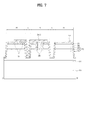
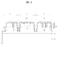
- FIG. 1 is a plan view illustrating a light emitting device 100 according to a first present invention.
- FIG. 2 is a sectional view taken along a direction of AA' of the light emitting device 100 illustrated in FIG. 1 .
- FIG. 3 is a sectional view taken along a direction of BB' of the light emitting device 100 illustrated in FIG. 1 .
- FIG. 4 is a sectional view taken along a direction of CC' of the light emitting device 100 illustrated in FIG. 1
- the light emitting device 100 includes a substrate 110, a buffer layer 115, a light emitting structure 120 divided into a plurality of light emitting regions P1 to Pn (in which n is a natural number greater than 1), a conductive layer 130, an insulating layer 140, a first electrode unit 150, at least one connection electrode 160-1 to 160-m (in which m is a natural number of 1 or more), at least one intermediate pad 182 and 184, and a second electrode unit 170.
- the substrate 110 may be formed with a carrier wafer, a material suitable for growth of semiconductor materials.
- the substrate 110 may be formed with a highly thermo-conductive material and may be a conductive substrate or an insulating substrate.
- the substrate 110 may contain at least one of sapphire (Al 2 0 3 ), GaN, SiC, ZnO, Si, GaP, InP, Ga 2 0 3 , and GaAs.
- a upper surface of the substrate 110 may be provided with a roughness.
- the buffer layer 115 is interposed between the substrate 110 and the light emitting structure 120 and may be formed with a Group III-V compound semiconductor.
- the buffer layer 115 functions to reduce difference in lattice constant between the substrate 110 and the light emitting structure 120.
- the light emitting structure 120 may be a semiconductor layer generating light and include a first conductive type semiconductor layer 122, an active layer 124, and a second conductive type semiconductor layer 126.
- the light emitting structure 120 may have a structure including the first conductive type semiconductor layer 122, the active layer 124, and the second conductive type semiconductor layer 126 sequentially stacked on the substrate 110.
- the first conductive type semiconductor layer 122 may be formed with a semiconductor compound.
- the first conductive type semiconductor layer 122 may be realized with a Group III-V or Group II-VI compound semiconductor or the like, and may be doped with a first conductive dopant.
- the first conductive type semiconductor layer 122 may be a semiconductor having a compositional formula of In x Al y Ga 1-x-y N (0 ⁇ x ⁇ 1, 0 ⁇ y ⁇ 1, 0 ⁇ x+y ⁇ 1).
- the first conductive type semiconductor layer 122 may contain any one of InAlGaN, GaN, AlGaN, InGaN, AlN, and InN and may be doped with an n-type dopant (for example, Si, Ge, or Sn).
- the active layer 124 is interposed between the first conductive type semiconductor layer 122 and the second conductive type semiconductor layer 126, and may generate light through energy generated during recombination of electrons and holes supplied from the first conductive type semiconductor layer 122 and the second conductive type semiconductor layer 126, respectively.
- the active layer 124 may be formed with a semiconductor compound, for example, a Group III-V or Group II-VI compound semiconductor, and may have a dobule-junction structure, a single well structure, a multiple well structure, a quantum wire structure or a quantum dot structure.
- a semiconductor compound for example, a Group III-V or Group II-VI compound semiconductor
- the active layer 124 When the active layer 124 is a single well structure or a quantum well structure, it may include a well layer having a compositional formula of In x Al y Ga 1-x-y N (0 ⁇ x ⁇ 1, 0 ⁇ y ⁇ 1, 0 ⁇ x+y ⁇ 1) and a barrier layer having a compositional formula of In a Al b Ga 1-a-b N (0 ⁇ a ⁇ 1, 0 ⁇ b ⁇ 1, 0 ⁇ a+b ⁇ 1).
- the well layer may be made of a material having a lower band gap than that of the barrier layer.
- the second conductive type semiconductor layer 126 may be formed with a semiconductor compound.
- the second conductive type semiconductor layer 126 may be realized with a Group III-V or Group II-VI compound semiconductor and be doped with a second conductive dopant.
- the second conductive type semiconductor layer 126 may be a semiconductor having a compositional formula of In x Al y Ga 1-x-y N (0 ⁇ x ⁇ 1, 0 ⁇ y ⁇ l, 0 ⁇ x+y ⁇ 1).
- the second conductive type semiconductor layer 126 may contain any one of GaN, A1N, AlGaN, InGaN, InN, InAlGaN, AlInN, AlGaAs, GaP, GaAs, GaAsP, and AlGaInP and be doped with a p-type dopant (for example, Mg, Zn, Ca, Sr, or Ba).
- the light emitting structure 120 may expose a part of the first conductive type semiconductor layer 122. That is, the light emitting structure 120 may expose a part of the first conductive type semiconductor layer 122 by etching the second conductive type semiconductor layer 126, the active layer 124 and the part of the first conductive type semiconductor layer 122. In this case, the surface of the first conductive type semiconductor layer 122 exposed by mesa-etching may be positioned to be lower than the lower surface of the active layer 124.
- a conductive clad layer may be interposed between the active layer 124 and the first conductive type semiconductor layer 122, or between the active layer 124 and the second conductive type semiconductor layer 126 and the conductive clad layer may be formed with a nitride semiconductor (for example, AlGaN).
- a nitride semiconductor for example, AlGaN
- the light emitting structure 120 may further include a third conductive semiconductor layer (not shown) disposed under the second conductive type semiconductor layer 126, and the third conductive semiconductor layer may have an opposite polarity to the second conductive type semiconductor layer 126.
- the first conductive type semiconductor layer 122 may be realized with an n-type semiconductor layer and the second conductive type semiconductor layer 126 may be realized with a p-type semiconductor layer. Accordingly, the light emitting structure 120 may include at least one ofN-P, P-N, N-P-N and P-N-P junction structures.
- the light emitting structure 120 may include a plurality of light emitting regions spaced from one another P1 to Pn (in which n is a natural number greater than 1) and at least one boundary region S.
- the boundary region S may be positioned between the light emitting regions P1 to Pn (in which n is a natural number greater than 1). Alternatively, the boundary region S may be positioned on the circumferences of the light emitting regions P1 to Pn (in which n is a natural number greater than 1).
- the boundary S may include a region where a part of the light emitting structure 120 is exposed, formed by mesa-etching the light emitting structure 120, in order to divide the light emitting structure 120 into a plurality of light emitting regions P1 to Pn (in which n is a natural number greater than 1). Areas of the light emitting regions P1 to Pn (in which n is a natural number greater than 1) may be identical, but the disclosure is not limited thereto.
- the light emitting structure 120 of a single chip may be divided into the light emitting regions P1 to Pn (in which n is a natural number greater than 1) through the boundary region S.
- the conductive layer 130 is disposed on the second conductive type semiconductor layer 126.
- the conductive layer 130 reduces total reflection and exhibits superior transmittance, thus increasing an extraction efficiency of light emitted from the active layer 124 to the second conductive type semiconductor layer 126.
- the conductive layer 130 may be realized with a single or multiple layer structure using one or more transparent oxide substances having high transmittance to light emission wavelengths, such as indium tin oxide (ITO), tin oxide (TO), indium zinc oxide (IZO), indium zinc tin oxide (IZTO), indium aluminum zinc oxide (IAZO), indium gallium zinc oxide (IGZO), indium gallium tin oxide (IGTO), aluminum zinc oxide (AZO), aluminum tin oxide (ATO), gallium zinc oxide (GZO), IrOx, RuOx, RuOx/ITO, Ni, Ag, Ni/IrOx/Au or Ni/IrOx/Au/ITO.
- the insulating layer 140 is positioned on the light emitting regions P1 to Pn (in which n is a natural number greater than 1) and the boundary region S.
- the insulating layer 140 may be formed of a light-transmissive insulating material, for example, SiO 2 , SiO x , SiO x N y , Si 3 N 4 , or Al 2 O 3 .
- the insulating layer 140 may cover upper parts and sides of the light emitting regions P1 to Pn (in which n is a natural number greater than 1) and cover the boundary region S.
- the first electrode unit 150 may include a first pad bonded to a wire (not shown) to supply a first power. In the present invention of FIG. 1 , the first electrode unit 150 may serve as the first pad.
- the second electrode unit 170 may contact the second conductive type semiconductor layer 126 or the conductive layer 130.
- the second electrode unit 170 may contact the conductive layer 130 of the last light emitting region (for example, P9) among the light emitting regions connected in series.
- the second electrode unit 170 may include a second pad 173 and a branch electrode 174 disposed on the insulating layer 140.
- the second pad 172 is bonded to a wire (not shown) to supply a power, and the branch electrode 174 extends from the second pad 172 and includes at least one portion 175 that passes through the insulating layer 140 and contacts the conductive layer 130.
- Each connection electrode may electrically connect the conductive layer 130 of one light emitting region (for example, P1) of two adjacent light emitting regions (for example, P1 and P2) to the first conductive type semiconductor layer 122 of the other light emitting region (for example, P2) thereof.
- connection electrode may electrically connect the second conductive type semiconductor layer 126 of one light emitting region (for example, P1) to the first conductive type semiconductor layer 122 of the other light emitting region (for example, P2).
- a plurality of light emitting regions P1 to Pn (in which n is a natural number greater than 1) connected to one another in series included in the light emitting device 100 are referred to as a 1 st light emitting region to an n th light emitting region in order. That is, the light emitting region in which the first electrode unit 150 is disposed is referred to as a 1 st light emitting region P1 and the light emitting region in which the second electrode unit 170 is disposed is referred to as an n th light emitting region Pn.
- adjacent light emitting regions may be a k th light emitting region and a K+1 th light emitting region
- the k th connection electrode may electrically connect the k th light emitting region to the K+1 th light emitting region in series, where 1 ⁇ k ⁇ (n-1).
- the k th connection electrode may electrically connect the second conductive type semiconductor layer 126 or conductive layer 130 of the k th light emitting region to the first conductive type semiconductor layer 122 of the k+1 th light emitting region.
- the k th connection electrode (for example, 160-1) may include at least one first portion (for example, 101) that passes through the insulating layer 140 and contacts the conductive layer 130 (or second conductive type semiconductor layer 126) of the k th light emitting region (for example, P1).
- the insulating layer 140 may be disposed between the light emitting structure 120 and the connection electrode 160-1 in the boundary S.
- the k th connection electrode may include at least one second portion (for example, 102) that passes through the insulating layer 140, the conductive layer 130, the second conductive type semiconductor layer 126, and the active layer 124 of the k+1 th light emitting region (for example, P2) and contacts the first conductive type semiconductor layer 122.
- the insulating layer 140 may be disposed between the K th connection electrode (for example, 160-1) and the conductive layer 130, between the second portion 102 of the K th connection electrode (for example, 160-1) and the second conductive type semiconductor layer 126, and between the second portion 102 of the connection electrode (for example, 160-1) and the active layer 124.
- mesa etching to expose the first conductive type semiconductor layer by etching the light emitting structure is performed.
- the light emitting region of the light emitting device is decreased in proportion to the mesh-etched region.
- the second portion (for example, 102) of the k th connection electrode (for example, 160-1) may have a structure of a hole or groove filled with an electrode material. For this reason, the light emitting region lost by mesa etching is decreased and in this present invention, a light emitting area may be increased.
- the insulating layer 140 functions to electrically insulate the k th connection electrode (for example, 160-1) from the conductive layer 130, the second conductive type semiconductor layer 126 and the active layer 124 of the k+1 th light emitting region (for example, P2).
- a lower surface 103 of the second portion 102 of the k th connection electrode (for example, 160-1) may be disposed to be lower than a lower surface of 104 of the active layer 124.
- the second portion 102 may have a structure of a hole or groove filled with an electrode material.
- the intermediate pads 182 and 184 are disposed on the insulating layer 140 in at least one of the light emitting regions P1 to Pn (in which n is a natural number greater than 1) and may be electrically connected to the second conductive type semiconductor layer 126 or the conductive layer 130.
- the intermediate pads 182 and 184 may be regions bonded to wires to supply a second power.
- the intermediate pads 182 and 184 may be disposed on the insulating layer 140 in at least one light emitting region (for example, P4 and P7) among the light emitting regions (for example, P2 to P8), other than light emitting regions (for example, P1 and P9) in which the first electrode unit 150 and the second electrode portion 172 are positioned.
- P4 and P7 among the light emitting regions (for example, P2 to P8), other than light emitting regions (for example, P1 and P9) in which the first electrode unit 150 and the second electrode portion 172 are positioned.
- the insulating layer 140 is interposed between the intermediate pad 182 or 184, and the conductive layer 130, and the intermediate pad (for example, 182) may be connected to any one (for example, 160-4) of the connection electrodes (for example, 160-3 and 160-4) disposed in the same light emitting region (for example, P4).
- the intermediate pad passes through the insulating layer and is directly connected to the conductive layer.
- the intermediate pad and the connection electrode positioned in the same light emitting region may be connected, or may be not connected.
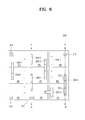
- FIG. 5 is a circuit diagram of the light emitting device 100 illustrated in FIG. 1 .
- the light emitting device 100 has a common single (-) terminal, for example, a first pad 150, and two or more (+) terminals, for example, a second pad 172 and at least one intermediate pad 182 and 184.
- the light emitting device includes a plurality of (+) terminals, pads 172, 182 and 184, thus enabling use of various driving voltages and enabling control of emission of light with various brightness levels.
- a driving voltage to drive one light emitting region is 3.4V
- a driving voltage applied to the light emitting device 100 is 13.6V
- a second power is applied to the first intermediate pad 182 to drive the first to fourth light emitting regions P1 to P4.
- a driving voltage applied to the light emitting device 100 is 23.8V
- a second power is applied to the second intermediate pad 184 to drive the first to seventh light emitting regions P1 to P7.
- a driving voltage applied to the light emitting device 100 is 30.6V
- a second power is applied to the second pad 172 to drive the first to ninth light emitting regions P1 to P9.
- This present invention may be designed such that a part or entirety of light emitting regions is driven by supplying a second power to any one of the intermediate pads 182 and 184, and the second pad 170 according to applied driving voltage.
- the light emitting area can be increased, current is dispersed and light-emission efficiency can thus be improved, because the connection electrodes 160-1 to 160-m (in which m is a natural number of 1 or more) point-contact the conductive layer 130 or the first conductive type semiconductor layer 122.
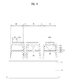
- FIG. 6 is a plan view illustrating a light emitting device 200 according to a second present invention.
- FIG. 7 is a sectional view taken along a direction of DD' of the light emitting device 200 illustrated in FIG. 6 .
- FIG. 8 is a sectional view taken along a direction of EE' of the light emitting device 200 illustrated in FIG. 6 .
- the same drawing reference numerals as in FIGs. 1 to 4 represent the same configuration and the aforementioned descriptions are omitted or summarized.
- the light emitting device 200 includes a substrate 110, a buffer layer 115, a light emitting structure 120 divided into a plurality of light emitting regions P1 to Pn (in which n is a natural number greater than 1), a conductive layer 130, an insulating layer 140, a first electrode unit 250, at least one connection electrode 260-1 to 260-m (in which m is a natural number of 1 or more), at least one intermediate pad 252 and 254, and a second electrode unit 272.
- the first electrode unit 250 may include a first pad bonded to a wire (not shown) to supply a first power. In the present invention of FIG. 6 , the first electrode unit 250 may serve as the first pad.
- the second electrode unit 272 is disposed on the conductive layer 130 in the first light emitting region P1 among the light emitting regions connected in series, and the first electrode unit 250 may be disposed on the first conductive type semiconductor layer 122 in the last light emitting region P9.
- the second electrode unit 272 may include a second pad bonded to a wire (not shown) to supply a second power.
- the second electrode unit 272 may further include a branch electrode (not shown) that extends from the second pad.
- the insulating layer 140 may be disposed in a plurality of light emitting regions P1 to Pn (in which n is a natural number greater than 1) and on the boundary S.
- Each connection electrode may electrically connect the first conductive type semiconductor layer 122 of one light emitting region (for example, P1) of adjacent light emitting regions (for example, P1 and P2) to the second conductive type semiconductor layer 126 or the conductive layer 130 in the other light emitting region (for example, P2) thereof.
- the k th connection electrode 260-k may electrically connect the second conductive type semiconductor layer 126 or the conductive layer 130 of the k+1 th light emitting region to the first conductive type semiconductor layer 122 of the k th light emitting region, where 1 ⁇ k ⁇ (n-1).
- the insulating layer 140 may be interposed between the light emitting structure 120 and the connection electrode 260-1 to 260-m (in which m is a natural number of 1 or more) in the boundary S.
- the intermediate pads 252 and 254 are disposed on the first conductive type semiconductor layer 122 of at least one of the light emitting regions P1 to Pn (in which n is a natural number greater than 1).
- the intermediate pads 252 and 254 may be bonded to wires (not shown) to supply a first power.
- a part of the first conductive type semiconductor layer 122 is exposed by mesa-etching at least one among the light emitting regions (for example, P2 to P8) and the intermediate pads 252, and 254 may be disposed on the part of the exposed first conductive type semiconductor layer 122.
- the intermediate pads 252 and 254 may be disposed on the first conductive type semiconductor layer 122 in at least one light emitting region (for example, P4 and P7) among the light emitting regions (for example, P2 to P8), other than light emitting regions (for example, P1 and P9) where the first electrode unit 250 and the second electrode unit 272 are positioned.
- P4 and P7 among the light emitting regions (for example, P2 to P8), other than light emitting regions (for example, P1 and P9) where the first electrode unit 250 and the second electrode unit 272 are positioned.
- FIG. 9 is a circuit diagram of the light emitting device 200 illustrated in FIG. 6 .
- the light emitting device 200 has a common single (+) terminal, for example, a second pad 272, and two or more (-) terminals, for example, a first pad 250 and at least one intermediate pad 252 and 254.
- the light emitting device includes two or more (-) terminals, pads 250, 252 and 254, thus enabling use of various driving voltages and enabling control of emission of light with various brightness levels.
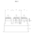
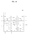
- FIG. 10 is a plan view illustrating a light emitting device 300 according to a third present invention.
- FIG. 11 is a sectional view taken along a direction of FF' of the light emitting device 300 illustrated in FIG. 10 .
- the light emitting device 300 includes a light emitting structure 10 divided into a plurality of light emitting regions P1 to Pn (in which n is a natural number greater than 1), a protective layer 20, a current blocking layer 30, a plurality of metal layers 40-1 to 40-n (in which n is a natural number greater than 1), an insulating layer 50, a second electrode unit 60, a passivation layer 25, a first electrode unit 92, at least one connection electrode 360-1 to 360-m (in which m is a natural number of 1 or more), and at least one intermediate pad 94 and 96.
- a light emitting structure 10 divided into a plurality of light emitting regions P1 to Pn (in which n is a natural number greater than 1), a protective layer 20, a current blocking layer 30, a plurality of metal layers 40-1 to 40-n (in which n is a natural number greater than 1), an insulating layer 50, a second electrode unit 60, a passivation layer 25, a first electrode unit 92
- the light emitting structure 10 may generate light and include a plurality of compound semiconductor layers containing Group III-V elements. As shown in FIG. 11 , the light emitting structure 10 may include a first conductive type semiconductor layer 16, an active layer 14 and a second conductive type semiconductor layer 12.
- the second conductive type semiconductor layer 12 may be positioned under the first conductive type semiconductor layer 16 and the active layer 14 may be positioned between the first conductive type semiconductor layer 16 and the second conductive type semiconductor layer 12.
- the light emitting structure 10 may include a plurality of light emitting regions spaced from one another P1 to Pn (in which n is a natural number greater than 1) and at least one boundary region S.
- the first conductive type semiconductor layer 16, the active layer 14 and the second conductive type semiconductor layer 12 may be the same, as described in FIGs. 1 and 2 .
- the protective layer 20 may be disposed under the boundary S.
- the protective layer 20 or the boundary S may define light emitting regions P1 to Pn (in which n is a natural number greater than 1).
- the protective layer 20 protects light emitting regions P1 to Pn (in which n is a natural number greater than 1) and thereby prevents deterioration in reliability of the light emitting device 300 during isolation etching to divide the light emitting structure 20 into a plurality of light emitting regions P1 to Pn (in which n is a natural number greater than 1).
- Each of the light emitting regions P1 to Pn may have a structure in which the second conductive type semiconductor layer 12, the active layer 14 and the first conductive type semiconductor layer 16 are stacked in a vertical direction.
- the vertical direction may be a direction from the second conductive type semiconductor layer 12 to the first conductive type semiconductor layer 16, or a direction vertical to the support layer 66.
- the metal layers 40-1 to 40-n may be disposed under the light emitting structure.
- the metal layers 40-1 to 40-n (in which n is a natural number greater than 1) may be spaced from one another under the second conductive type semiconductor layer 12 in the corresponding one of the light emitting regions P1 to Pn (in which n is a natural number greater than 1).
- FIG. 11 illustrates only metal layers 40-7, 40-8 and 40-9 corresponding to the light emitting regions P7, P8 and P9, respectively, and does not illustrate metal layers 40-1 to 40-6 corresponding to other light emitting regions P1 to P6.
- the ohmic layer 42 may contain at least one of In, Zn, Ag, Sn, Ni, and Pt.
- the reflective layer 44 may contact the outermost side of the ohmic layer 42 and surround the ohmic layer 42.
- the reflective layer 44 may contain at least one of a reflective metal or an alloy thereof for example, Ag, Ni, Al, Rh, Pd, Ir, Ru, Mg, Zn, Pt, Au, and Hf.
- the reflective layer 44 may have a single or multiple layer structure using a light-transmissive conductive oxide, for example, indium zinc oxide (IZO), indium zinc tin oxide (IZTO), indium aluminum zinc oxide (IAZO), indium gallium zinc oxide (IGZO), indium gallium tin oxide (IGTO), aluminum zinc oxide (AZO), antimony tin oxide (ATO) or the like.
- the reflective layer 44 may have a multilayer structure containing a composite of metal and conductive oxide, such as IZO/Ni, AZO/Ag, IZO/Ag/Ni, or AZO/Ag/Ni.
- the reflective layer 44 ohmic-contacts the second conductive type semiconductor layer 12 by using a material for the reflective layer 44 as a material that ohmic-contacts the second conductive type semiconductor layer 12.
- the current blocking layer 30 may be disposed under the second conductive type semiconductor layer 12 in the light emitting structure 10.
- the current blocking layer 30 may be disposed to correspond to the connection electrodes 360-1 to 360-m (in which m is a natural number of 1 or more), or the first electrode unit 92, or intermediate pads 94 and 96, and at least partially overlaps the connection electrodes 360-1 to 360-m, or the first electrode unit 92, or intermediate pads 94 and 96 in a vertical direction.
- the current blocking layer 30 may have a pattern corresponding to a pattern of the connection electrode 360-1 to 360-m (in which m is a natural number of 1 or more).
- the vertical direction may be a direction from the second conductive type semiconductor layer 12 to the first conductive type semiconductor layer 16.
- the current blocking layer 30 may be formed with a material having a lower electrical conductivity than metal layers 40-1 to 40-n (in which n is a natural number greater than 1), a material that Schottky-contacts the second conductive type semiconductor layer 12, or an electrical insulating material.
- the current blocking layer 30 may contain at least one of ZnO, SiO 2 , SiON, Si 3 N 4 , Al 2 O 3 ,TiO 2 , Ti, Al, and Cr.
- the second electrode unit 60 is positioned under the insulating layer 50 and may be electrically connected to the metal layer (for example, 40-9) that contacts the second conductive type semiconductor layer 12 in one (for example, P9) of the light emitting regions.
- the second electrode unit 60 may supply a second power to the one light emitting region (for example, P9).
- the second electrode unit 60 may include a barrier layer, 62, a bonding layer 64 and a support layer 66.
- the barrier layer 62 contains a barrier metal material, for example at least one of Pt, Ti, W, V, Fe, and Mo, and may have a single or multiple layer structure.
- the barrier layer 62 is positioned under the insulating layer 50 and may be electrically connected to the metal layer (for example, 40-9) that contacts the second conductive type semiconductor layer 12 in one (for example, P9) of the light emitting regions.
- the second conductive type semiconductor layer 12 positioned in the ninth light emitting region (for example, P9) among the light emitting regions P1 to Pn (in which n is a natural number greater than 1) is electrically connected to the barrier layer 62, the second power may be supplied through the barrier layer 62 to the ninth light emitting region (for example, P9).
- the barrier layer 62 is electrically connected to the support layer 66 described below and the second power may be supplied through the support layer 66.
- the insulating layer 50 may be formed with an insulating material, for example, at least one of Al 2 O 3 , SiO 2 , Si 3 N 4 , TiO 2 , and AlN, and may have a single or multiple layer structure.
- the support layer 66 is disposed under the barrier layer 62, supports the light emitting structure 10, and supplies power to the light emitting structure 10, together with the first electrode unit 92.
- the support layer 66 is a conductive material and is a semiconductor material containing a metal material such as copper (Cu), gold (Au), nickel (Ni), molybdenum (Mo), or copper-tungsten (Cu-W), or at least one of Si, Ge, GaAs, ZnO, SiC, and SiGe.
- the bonding layer 64 is disposed between the barrier layer 62 and the support layer 66.
- the bonding layer 64 is interposed between the barrier layer 62 and the support layer 66 to bond the two layers.
- the bonding layer 64 is formed to bond the support layer 66 in a bonding manner. For this reason, when the support layer 66 is formed using a method such as plating or deposition, or the support layer 66 is a semiconductor layer, the bonding layer 64 may be omitted.
- the bonding layer 64 contains a bonding metal material, for example, at least one of Au, Sn, Ni, Nb, In, Cu, Ag and Pd.
- the first electrode unit 92 may include a first pad bonded to a wire to supply a first power. In the present invention of FIG. 10 , the first electrode unit 92 may serve as the first pad.
- the upper surface of the first conductive type semiconductor layer 16 may be provided with a roughness 16-1 in order to improve light extraction efficiency.
- the passivation layer 25 may be disposed in the light emitting regions P1 to Pn (in which n is a natural number greater than 1) and the boundary region S.
- the passivation layer 25 may be disposed on the protective layer 20 of the boundary S.
- the first electrode unit 92 may be exposed from the passivation layer 25.
- connection electrodes 360-1 to 360-m may be disposed on the passivation layer 25 positioned in adjacent light emitting regions and boundary region provided therebetween.
- connection electrode 360-1 to 360-m electrically connects the first conductive type semiconductor layer 16 in one light emitting region of adjacent light emitting regions to the second conductive type semiconductor layer 12 in the other light emitting region thereof.
- the k th connection electrode (for example, 360-1) may electrically connect the second conductive type semiconductor layer 12 of the k th light emitting region to the first conductive type semiconductor layer 16 of the K+1 th light emitting region.
- connection electrode 360-1 to 360-m may include at least one first portion that passes through the passivation layer 25, the first conductive type semiconductor layer 16 and the active layer 14, and contacts the second conductive type semiconductor layer 12 in one of adjacent light emitting regions.
- connection electrode 360-1 to 360-m may include at least one second portion that passes through the passivation layer 25 and contacts the first conductive type semiconductor layer 16 in the other of the adjacent light emitting regions.
- the passivation layer 25 may serve as an insulating layer that electrically insulates the first portion 301 of the k th connection electrode (for example, 360-7) from the first conductive type semiconductor layer 16 and the active layer 14 in the K th light emitting region (for example, P7).
- a lower surface of the first portion 301 of the k th connection electrode may be disposed to be lower than a lower surface of the active layer 124.
- the first portion 301 may have a structure of a hole or groove filled with an electrode material.
- the intermediate pads 94 and 96 are disposed on the first conductive type semiconductor layer 16 in at least one of the light emitting regions P1 to Pn (in which n is a natural number greater than 1) and may be electrically connected to the first conductive type semiconductor layer 16.
- the intermediate pads 94 and 96 may be bonded to wires (not shown) to supply a second power.
- the intermediate pads 94 and 96 may be disposed on the first conductive type semiconductor layer 16 in at least one (for example, P4 and P7) of light emitting regions (for example, P2 to P8) other than a light emitting region (for example, P1) in which the first electrode unit 92 is disposed, and a light emitting region (for example, P9) connected to the metal layer (for example, 40-9) electrically connected to the second electrode unit 60.
- the intermediate pad (for example, 94) may be electrically isolated or separated from the connection electrode (for example, 360-3) disposed in the same light emitting region (for example, P4).
- the intermediate pad may be electrically connected to the connection electrode (for example, 360-3) disposed in the same light emitting region (for example, P4).
- This present invention may be designed such that a part or entirety of light emitting regions P1 to Pn (in which n is a natural number of 1 or more) is driven by supplying a first power to any one of the first electrode unit 92 and the intermediate pads 94 and 96 according to applied driving voltage.
- FIG. 12 is a sectional view illustrating a light emitting device package including a light emitting device in accordance with one present invention.
- the light emitting device package includes a package body 510, a first lead frame 512, a second lead frame 514, a light emitting device 520, a reflective plate 530, wires 522 and 524, and a resin layer 540.
- the package body 510 has a structure with a cavity at one side region thereof. Here, the side wall of the cavity may be inclined.
- the package body 510 may be formed of a substrate having excellent insulation and thermal conductivity, such as a silicon-based wafer level package, a silicon substrate, silicon carbide (SiC), aluminum nitride (AlN), or the like, and may have a structure in which plural substrates are stacked. This present invention is not limited to the above-described material, structure and shape of the package body 510.
- the first lead frame 512 and the second lead frame 514 are disposed on the surface of the package body 510 so as to be electrically separated from each other in consideration of heat dissipation or mounting of the light emitting device 520.
- the light emitting device 520 is electrically connected to the first lead frame 512 and the second lead frame 514 through the first wire 522 and the second wire 524.
- the light emitting device 520 may be one of the light emitting devices 100, 200 and 300 according to the afore-mentioned present inventions.
- the first electrode unit 150 is electrically connected to the second lead frame 514 through the second wire 524.
- one of the second pad 172 of the second electrode unit 170 and the intermediate pads 182 and 184 may be electrically connected to the first lead frame 512 through the first wire 522.
- the second electrode unit 272 is electrically connected to the first lead frame 512 through the first wire 522.
- one of the first electrode unit 250 and intermediate pads 252 and 254 may be electrically connected to the second lead frame 514 through the second wire 524.
- the support layer 66 is bonded to the first lead frame 512.
- one of the first electrode unit 92 and intermediate pads 94 and 96 may be electrically connected to the second lead frame 514 through the second wire 524.
- the reflective plate 530 may be formed on the side wall of the cavity of the package body 510 to guide light emitted from the light emitting device 520 in a designated direction.
- the reflective plate 530 may be formed of a light reflective material, for example, metal coating or metal flakes.
- the resin layer 540 surrounds the light emitting device 520 located within the cavity of the package body 510, and protects the light emitting device 520 from external environments.
- the resin layer 540 may be formed of a colorless transparent polymer resin material, such as epoxy or silicon.
- the resin layer 540 may include phosphors to change the wavelength of light emitted from the light emitting device 520.
- the light emitting device packages may include at least one of light emitting devices according to the afore-mentioned present inventions, but the disclosure is not limited thereto.
- An array of plural light emitting device packages in accordance with this present invention may be mounted on a substrate, and optical members, such as a light guide panel, a prism sheet, a diffusion sheet, etc., may be disposed on an optical path of the light emitting device packages.
- optical members such as a light guide panel, a prism sheet, a diffusion sheet, etc.
- the light emitting device packages, the substrate and the optical members may function as a backlight unit.
- the light emitting devices or the light emitting device package in accordance with the above-described present inventions may constitute a display apparatus, an indicating apparatus and a lighting system, and, for example, the lighting system may include a lamp or a streetlight.
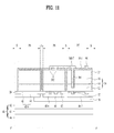
- FIG. 13 is an exploded perspective view of a lighting apparatus including light emitting device packages in accordance with one present invention.
- the lighting apparatus in accordance with this present invention includes a light source 750 to project light, a housing 700 in which the light source 750 is installed, a heat dissipation unit 740 to dissipate heat generated by the light source 750, and a holder 760 to couple the light source 750 and the heat dissipation unit 740 to the housing 700.
- the housing 700 includes a socket connector 710 connected to an electrical socket (not shown) and a body 730 connected to the socket connector 710 and accommodating the light source 750.
- One air flow hole 720 may be formed through the body 730.
- a plurality of air flow holes 720 may be provided on the body 730 of the housing 700.
- One air flow hole 720 may be formed, or plural air flow holes 720 may be arranged, in a radial shape or various other shapes.
- the light source 750 includes a plurality of light emitting device packages 752 provided on a substrate 754.
- the substrate 754 may have a shape which is capable of being inserted into an opening of the housing 700, and be formed of a material having high thermal conductivity so as to transfer heat to the heat dissipation unit 740, as described later.
- a plurality of light emitting device package may a light emitting device package according to the aforementioned present invention.
- the holder 760 is provided under the light source 750.
- the holder 760 may include a frame and air flow holes. Further, although not shown in FIG. 12 , optical members may be provided under the light source 750 so as to diffuse, scatter or converge light emitted from the light emitting device packages 752 of the light source 750.
- FIG. 14 is an exploded perspective view of a display apparatus 800 including light emitting device packages according to one present invention.
- the display apparatus 800 includes a bottom cover 810, a reflective plate 820 disposed on the bottom cover 810, light emitting modules 830 and 835 to emit light, a light guide plate 840 disposed on the front surface of the reflective plate 820 to guide light emitted from the light emitting modules 830 and 835 to the front part of the display device, an optical sheet including prism sheets 850 and 860 disposed on the front surface of the light guide plate 840, a display panel 870 disposed on the front surface of the optical sheet, an image signal output circuit 872 connected to the display panel 870 to supply an image signal to the display panel 870, and a color filter 880 disposed on the front surface of the display panel 870.
- the bottom cover 810, the reflective plate 820, the light emitting modules 830 and 835, the light guide plate 840, and the optical sheet may constitute a backlight unit.
- the light emitting modules may include a light emitting device package 835 on the substrate 830.
- the substrate 830 may be formed of PCB or the like.
- the light emitting device package 835 may be the light emitting device package according to the afore-mentioned present invention.
- the bottom cover 810 may accommodate components within the image display apparatus 800.
- the reflective plate 820 may be provided as a separate component, as shown in FIG. 13 , or be provided by coating the rear surface of the light guide plate 840 or the front surface of the bottom cover 810 with a material having high reflectivity.
- the reflective plate 820 may be formed of a material that has high reflectivity and may be useful in an ultra-thin form, such as polyethylene terephthalate (PET).
- PET polyethylene terephthalate
- the light guide plate 840 is formed of a material having a high index of refraction and high transmittance, such as polymethylmethacrylate (PMMA), polycarbonate (PC) or polyethylene (PE).
- PMMA polymethylmethacrylate
- PC polycarbonate
- PE polyethylene
- the first prism sheet 850 is formed of a light transmitting and elastic polymer on one surface of a support film, and the polymer may have a prism layer in which plural three-dimensional structures are repeated.
- plural patterns may be formed in a strip manner in which ridges and valleys are repeated, as shown in the drawing.
- a direction of ridges and valleys formed on one surface of a support film of the second prism sheet 860 may be perpendicular to a direction of the ridges and the valleys formed on one surface of the support film of the first prism sheet 850. This serves to uniformly distribute light transmitted from the light source module and the reflective plate 820 in all directions of the panel 870.
- a diffusion sheet may be disposed between the light guide plate 840 and the first prism sheet 850.
- the diffusion sheet may be made of polyester and polycarbonate and maximizes a light projection angle of light emitted from the backlight unit through refraction and scattering.
- the diffusion sheet may include a support layer including a light diffusion agent, and a first layer and a second layer that are formed on a light projection surface (first prism sheet direction) and a light incident surface (reflective sheet direction) and do not include a light diffusion agent.
- optical sheets may include another combination, for example, a micro lens array, a combination of a diffusion sheet and a micro lens array, or a combination of one prism sheet and a micro lens array.
- a liquid crystal display panel may be provided, or other kinds of display apparatuses requiring a light source may be provided instead of the liquid crystal display panel.
- the light emitting device controls emission of light with various brightness levels, increases a light emitting area and disperses current, thus improving light emission efficiency.
Abstract
Description
- Present inventions relate to a light emitting device, a light emitting device package, a lighting apparatus, and a display apparatus.
- Red, green and blue light emitting diodes (LED) capable of realizing high luminance and white light were developed, based on development of metal organic chemical vapor deposition and molecular beam growth of gallium nitride (GaN).
- Such LEDs do not contain environmentally harmful substances such as mercury (Hg) used in conventional lighting apparatuses such as incandescent lamps or fluorescent lamps and thus advantageously have superior eco-friendliness, long lifespan and low power consumption, thus being used as alternatives of conventional light sources. The key factors in competitiveness of such LEDs are to realize high luminance, based on chips with high efficiency and high power and packaging technologies.
- In order to realize high luminance, an increase in light extraction efficiency is important. A variety of methods using flip-chip structures, surface texturing, patterned sapphire substrates (PSSs), photonic crystal techniques, anti-reflective layer structures and the like are being researched in order to increase light extraction efficiency.
- In general, a light emitting device may include a light emitting structure to generate light, a first electrode and a second electrode to receive power, a current blocking layer to disperse light, an ohmic layer that ohmic-contacts the light emitting structure, and a reflective layer to improve light extraction efficiency. The structure of a general light emitting device is disclosed in Korean Patent Laid-open No.
10-2011-0041270 - Present inventions provide a light emitting device to control emission of light with various brightness levels and increase an area of light emitting regions.
- In one present invention, a light emitting device includes: a light emitting structure divided into a plurality of light emitting regions including a first semiconductor layer, an active layer and a second semiconductor layer and at least one boundary region disposed between the light emitting regions; a first electrode unit disposed on the first semiconductor layer in one of the light emitting regions; a second electrode unit disposed on the second semiconductor layer in another of the light emitting regions; at least one connection electrode to electrically connect the first semiconductor layer of one of adjacent light emitting regions to the second semiconductor layer of the other thereof; and an intermediate pad disposed on the second semiconductor layer in at least one of the light emitting regions, wherein the light emitting regions are connected in series through the connection electrode.
- In another present invention, a light emitting device includes: a light emitting structure divided into a plurality of light emitting regions including a first semiconductor layer, an active layer and a second semiconductor layer; and at least one boundary region disposed between the light emitting regions; a first electrode unit disposed on the first semiconductor layer in one of the light emitting regions; a second electrode unit disposed on the second semiconductor layer in another of the light emitting regions; at least one connection electrode to electrically connect the first semiconductor layer of one of adjacent light emitting regions to the second semiconductor layer of the other thereof; and an intermediate pad disposed on the first semiconductor layer in at least one of the light emitting regions, wherein the light emitting regions are connected in series through the connection electrode.
- The intermediate pad may be disposed on the second semiconductor layer in at least one of light emitting regions, other than light emitting regions in which the first electrode unit and the second electrode unit are positioned. Alternatively, the intermediate pad may be disposed on the first semiconductor layer in at least one of light emitting regions, other than light emitting regions in which the first electrode unit and the second electrode unit are positioned.
- Each of the first electrode unit and the second electrode unit may include a pad to receive a power.
- The intermediate pad may be electrically connected to the connection electrode disposed in the same light emitting region.
- The light emitting device may further include: an insulating layer disposed in the light emitting regions and the boundary region, wherein the connection electrode is disposed on the insulating layer.
- The intermediate pad may be separated from the connection electrode on the insulating layer in the same light emitting region. Alternatively, the intermediate pad may be integrated with the connection electrode on the insulating layer in the same light emitting region. The connection electrode may include a first portion that passes through the insulating layer and contacts the second semiconductor layer in one of the adjacent light emitting regions. The connection electrode may further include a second portion that passes through the insulating layer, the second semiconductor layer and the active layer, and contacts the first semiconductor layer in the other of the adjacent light emitting regions, wherein the insulating layer is disposed between the second portion and the second semiconductor layer, and between the second portion and the active layer.
- A lower surface of the second portion of the connection electrode may be positioned to be lower than a lower surface of the active layer.
- The light emitting device may further include: a substrate disposed under the light emitting structure; and a conductive layer disposed between the light emitting region and the insulating layer.
- The second portion may pass through the conductive layer. The insulating layer may be disposed between the second portion and the conductive layer.
- The first electrode unit may receive a first power, and at least one of the second electrode unit and the intermediate pad may receive a second power. Alternatively, one of the first electrode unit and the intermediate pad may receive a first power, and the second electrode unit may receive a second power.
- In another present invention, a light emitting device includes: a light emitting structure divided into a plurality of light emitting regions including a first semiconductor layer, an active layer and a second semiconductor layer; and at least one boundary region disposed between the light emitting regions; a first electrode unit disposed on the first semiconductor layer in one of the light emitting regions; a plurality of metal layers disposed under the second semiconductor layers in the respective light emitting regions; a second electrode unit electrically connected to the metal layer disposed under the second semiconductor layer in another of the light emitting regions; an insulating layer to electrically insulate the metal layers from each other; at least one connection electrode to electrically connect the first semiconductor layer of one of adjacent light emitting regions to the second semiconductor layer of the other thereof; and an intermediate pad disposed on the first semiconductor layer in at least one of the light emitting regions, wherein the light emitting regions are connected in series through the connection electrode.
- Each metal layer may include at least one of an ohmic layer and a reflective layer.
- The intermediate pad may be disposed on the first semiconductor layer in at least one of light emitting regions, other than a light emitting region, in which the first electrode unit is positioned, and a light emitting region, with which the second electrode unit is electrically connected.
- The light emitting device may further include: a passivation layer disposed in the light emitting regions and the boundary region, wherein the connection electrode is disposed on the passivation layer.
- The connection electrode may include: at least one first portion that passes through the passivation layer, the first semiconductor layer and the active layer, and contacts the second semiconductor layer in one of the adjacent light emitting regions; and at least one second portion that passes through the passivation layer, and contacts the first semiconductor layer in the other of the adjacent light emitting regions, wherein the passivation layer is disposed between the first portion and the first semiconductor layer, and between the first portion and the active layer.
- The second electrode unit may include: a barrier layer electrically connected to the metal layer disposed under the second semiconductor layer in the another of the light emitting regions; and a support layer disposed under the barrier layer.
- The light emitting device may further include: a current blocking layer disposed between the second semiconductor layer and the metal layer in each light emitting region, such that it corresponds to the connection electrode or the intermediate pad, the current blocking layer at least partially overlapping the connection electrode or the intermediate pad in a vertical direction.
- The insulating layer may electrically insulate metal layers other than the metal layer electrically connected to the second electrode unit, from the second electrode unit.
- Arrangements and present inventions may be described in detail with reference to the following drawings in which like reference numerals refer to like elements and wherein:
-
FIG. 1 is a plan view illustrating a light emitting device according to a first present invention; -
FIG. 2 is a sectional view taken along a direction of AA' of the light emitting device illustrated inFIG. 1 ; -
FIG. 3 is a sectional view taken along a direction of BB' of the light emitting device inFIG. 1 ; -
FIG. 4 is a sectional view taken along a direction of CC' of the light emitting device inFIG. 1 ; -
FIG. 5 is a circuit diagram of the light emitting device illustrated inFIG. 1 ; -
FIG. 6 is a plan view illustrating a light emitting device according to a second present invention; -
FIG. 7 is a sectional view taken along a direction of DD' of the light emitting device illustrated inFIG. 6 ; -
FIG. 8 is a sectional view taken along a direction of EE' of the light emitting device illustrated inFIG. 6 ; -
FIG. 9 is a circuit diagram of the light emitting device illustrated inFIG. 6 ; -
FIG. 10 is a plan view illustrating a light emitting device according to a third present invention; -
FIG. 11 is a sectional view taken along a direction of FF' of the light emitting device illustrated inFIG. 10 ; -
FIG. 12 is a sectional view illustrating a light emitting device package including a light emitting device according to one present invention; -
FIG. 13 is an exploded perspective view of a lighting apparatus including the light emitting device package according to one present invention; and -
FIG. 14 is an exploded perspective view of a display apparatus including the light emitting device package according to one present invention. - Hereinafter, present inventions will be clearly understood from description with reference to the annexed drawings.
- It will be understood that when an element is referred to as being "on" or "under" another element, it can be directly on/under the element, and one or more intervening elements may also be present. When an element is referred to as being 'on' or 'under', 'under the element' as well as 'on the element' can be included based on the element.
- In the drawings, the thickness or size of each layer is exaggerated, omitted, or schematically illustrated for convenience of description and clarity. Also, the size or area of each constituent element does not entirely reflect the actual size thereof. Hereinafter, a light emitting device, a method for manufacturing the same and a light emitting package including the light emitting device according to present inventions will be described with reference to the annexed drawings.
-
FIG. 1 is a plan view illustrating alight emitting device 100 according to a first present invention.FIG. 2 is a sectional view taken along a direction of AA' of thelight emitting device 100 illustrated inFIG. 1 .FIG. 3 is a sectional view taken along a direction of BB' of thelight emitting device 100 illustrated inFIG. 1 .FIG. 4 is a sectional view taken along a direction of CC' of thelight emitting device 100 illustrated inFIG. 1 - Referring to
FIGs. 1 to 4 , thelight emitting device 100 includes asubstrate 110, abuffer layer 115, alight emitting structure 120 divided into a plurality of light emitting regions P1 to Pn (in which n is a natural number greater than 1), aconductive layer 130, aninsulating layer 140, afirst electrode unit 150, at least one connection electrode 160-1 to 160-m (in which m is a natural number of 1 or more), at least oneintermediate pad second electrode unit 170. - The
substrate 110 may be formed with a carrier wafer, a material suitable for growth of semiconductor materials. In addition, thesubstrate 110 may be formed with a highly thermo-conductive material and may be a conductive substrate or an insulating substrate. For example, thesubstrate 110 may contain at least one of sapphire (Al203), GaN, SiC, ZnO, Si, GaP, InP,Ga 203, and GaAs. A upper surface of thesubstrate 110 may be provided with a roughness. - The
buffer layer 115 is interposed between thesubstrate 110 and thelight emitting structure 120 and may be formed with a Group III-V compound semiconductor. Thebuffer layer 115 functions to reduce difference in lattice constant between thesubstrate 110 and thelight emitting structure 120. - The
light emitting structure 120 may be a semiconductor layer generating light and include a first conductivetype semiconductor layer 122, anactive layer 124, and a second conductivetype semiconductor layer 126. Thelight emitting structure 120 may have a structure including the first conductivetype semiconductor layer 122, theactive layer 124, and the second conductivetype semiconductor layer 126 sequentially stacked on thesubstrate 110. - The first conductive
type semiconductor layer 122 may be formed with a semiconductor compound. The first conductivetype semiconductor layer 122 may be realized with a Group III-V or Group II-VI compound semiconductor or the like, and may be doped with a first conductive dopant. - For example, the first conductive
type semiconductor layer 122 may be a semiconductor having a compositional formula of InxAlyGa1-x-yN (0≤x≤1, 0≤y≤1, 0≤x+y≤1). For example, the first conductivetype semiconductor layer 122 may contain any one of InAlGaN, GaN, AlGaN, InGaN, AlN, and InN and may be doped with an n-type dopant (for example, Si, Ge, or Sn). - The
active layer 124 is interposed between the first conductivetype semiconductor layer 122 and the second conductivetype semiconductor layer 126, and may generate light through energy generated during recombination of electrons and holes supplied from the first conductivetype semiconductor layer 122 and the second conductivetype semiconductor layer 126, respectively. - The
active layer 124 may be formed with a semiconductor compound, for example, a Group III-V or Group II-VI compound semiconductor, and may have a dobule-junction structure, a single well structure, a multiple well structure, a quantum wire structure or a quantum dot structure. - When the
active layer 124 is a single well structure or a quantum well structure, it may include a well layer having a compositional formula of InxAlyGa1-x-yN (0≤x≤1, 0≤y≤1, 0≤x+y≤1) and a barrier layer having a compositional formula of InaAlbGa1-a-bN (0≤a≤1, 0≤b≤1, 0≤a+b≤1). The well layer may be made of a material having a lower band gap than that of the barrier layer. - The second conductive
type semiconductor layer 126 may be formed with a semiconductor compound. The second conductivetype semiconductor layer 126 may be realized with a Group III-V or Group II-VI compound semiconductor and be doped with a second conductive dopant. - For example, the second conductive
type semiconductor layer 126 may be a semiconductor having a compositional formula of InxAlyGa1-x-yN (0≤x≤1, 0≤y≤l, 0≤x+y≤1). For example, the second conductivetype semiconductor layer 126 may contain any one of GaN, A1N, AlGaN, InGaN, InN, InAlGaN, AlInN, AlGaAs, GaP, GaAs, GaAsP, and AlGaInP and be doped with a p-type dopant (for example, Mg, Zn, Ca, Sr, or Ba). - The
light emitting structure 120 may expose a part of the first conductivetype semiconductor layer 122. That is, thelight emitting structure 120 may expose a part of the first conductivetype semiconductor layer 122 by etching the second conductivetype semiconductor layer 126, theactive layer 124 and the part of the first conductivetype semiconductor layer 122. In this case, the surface of the first conductivetype semiconductor layer 122 exposed by mesa-etching may be positioned to be lower than the lower surface of theactive layer 124. - A conductive clad layer (not shown) may be interposed between the
active layer 124 and the first conductivetype semiconductor layer 122, or between theactive layer 124 and the second conductivetype semiconductor layer 126 and the conductive clad layer may be formed with a nitride semiconductor (for example, AlGaN). - The
light emitting structure 120 may further include a third conductive semiconductor layer (not shown) disposed under the second conductivetype semiconductor layer 126, and the third conductive semiconductor layer may have an opposite polarity to the second conductivetype semiconductor layer 126. The first conductivetype semiconductor layer 122 may be realized with an n-type semiconductor layer and the second conductivetype semiconductor layer 126 may be realized with a p-type semiconductor layer. Accordingly, thelight emitting structure 120 may include at least one ofN-P, P-N, N-P-N and P-N-P junction structures. - The
light emitting structure 120 may include a plurality of light emitting regions spaced from one another P1 to Pn (in which n is a natural number greater than 1) and at least one boundary region S. The boundary region S may be positioned between the light emitting regions P1 to Pn (in which n is a natural number greater than 1). Alternatively, the boundary region S may be positioned on the circumferences of the light emitting regions P1 to Pn (in which n is a natural number greater than 1). The boundary S may include a region where a part of thelight emitting structure 120 is exposed, formed by mesa-etching thelight emitting structure 120, in order to divide thelight emitting structure 120 into a plurality of light emitting regions P1 to Pn (in which n is a natural number greater than 1). Areas of the light emitting regions P1 to Pn (in which n is a natural number greater than 1) may be identical, but the disclosure is not limited thereto. - The
light emitting structure 120 of a single chip may be divided into the light emitting regions P1 to Pn (in which n is a natural number greater than 1) through the boundary region S. - The
conductive layer 130 is disposed on the second conductivetype semiconductor layer 126. Theconductive layer 130 reduces total reflection and exhibits superior transmittance, thus increasing an extraction efficiency of light emitted from theactive layer 124 to the second conductivetype semiconductor layer 126. Theconductive layer 130 may be realized with a single or multiple layer structure using one or more transparent oxide substances having high transmittance to light emission wavelengths, such as indium tin oxide (ITO), tin oxide (TO), indium zinc oxide (IZO), indium zinc tin oxide (IZTO), indium aluminum zinc oxide (IAZO), indium gallium zinc oxide (IGZO), indium gallium tin oxide (IGTO), aluminum zinc oxide (AZO), aluminum tin oxide (ATO), gallium zinc oxide (GZO), IrOx, RuOx, RuOx/ITO, Ni, Ag, Ni/IrOx/Au or Ni/IrOx/Au/ITO. - The insulating
layer 140 is positioned on the light emitting regions P1 to Pn (in which n is a natural number greater than 1) and the boundary region S. The insulatinglayer 140 may be formed of a light-transmissive insulating material, for example, SiO2, SiOx, SiOxNy, Si3N4, or Al2O3. For example, the insulatinglayer 140 may cover upper parts and sides of the light emitting regions P1 to Pn (in which n is a natural number greater than 1) and cover the boundary region S. - The
first electrode unit 150 is disposed on the first conductivetype semiconductor layer 122 in one light emitting region (for example, P1) of the light emitting regions P1 to Pn (for example, n=9) and may contact the first conductivetype semiconductor layer 122. Thefirst electrode unit 150 may include a first pad bonded to a wire (not shown) to supply a first power. In the present invention ofFIG. 1 , thefirst electrode unit 150 may serve as the first pad. - The
second electrode unit 170 is disposed on the second conductivetype semiconductor layer 126 in another light emitting region (for example, P9) among the light emitting regions P1 to Pn (for example, n=9). Thesecond electrode unit 170 may contact the second conductivetype semiconductor layer 126 or theconductive layer 130. For example, thesecond electrode unit 170 may contact theconductive layer 130 of the last light emitting region (for example, P9) among the light emitting regions connected in series. - The
second electrode unit 170 may include a second pad 173 and abranch electrode 174 disposed on the insulatinglayer 140. Thesecond pad 172 is bonded to a wire (not shown) to supply a power, and thebranch electrode 174 extends from thesecond pad 172 and includes at least oneportion 175 that passes through the insulatinglayer 140 and contacts theconductive layer 130. - The connection electrodes 160-1 to 160-m (for example, m=8) are disposed on the insulating
layer 140 and electrically connect a plurality of light emitting regions P1 to Pn (for example, n=9) in series. For example, the connection electrodes 160-1 to 160-m (for example, m=8) connect a plurality of light emitting regions P1 to P9 in series, from a first light emitting region P1, in which thefirst electrode unit 150 is disposed, as a start point, to the ninth light emitting region P9 in which thesecond electrode unit 170 is disposed, as an end point. - Each connection electrode (for example, 160-1) may electrically connect the
conductive layer 130 of one light emitting region (for example, P1) of two adjacent light emitting regions (for example, P1 and P2) to the first conductivetype semiconductor layer 122 of the other light emitting region (for example, P2) thereof. - In another present invention excluding the
conductive layer 130, the connection electrode (for example, 160-1) may electrically connect the second conductivetype semiconductor layer 126 of one light emitting region (for example, P1) to the first conductivetype semiconductor layer 122 of the other light emitting region (for example, P2). - A plurality of light emitting regions P1 to Pn (in which n is a natural number greater than 1) connected to one another in series included in the
light emitting device 100 are referred to as a 1st light emitting region to an nth light emitting region in order. That is, the light emitting region in which thefirst electrode unit 150 is disposed is referred to as a 1st light emitting region P1 and the light emitting region in which thesecond electrode unit 170 is disposed is referred to as an nth light emitting region Pn. Here, "adjacent light emitting regions" may be a kth light emitting region and a K+1th light emitting region, the kth connection electrode may electrically connect the kth light emitting region to the K+1th light emitting region in series, where 1≤k≤(n-1). - That is, the kth connection electrode may electrically connect the second conductive
type semiconductor layer 126 orconductive layer 130 of the kth light emitting region to the first conductivetype semiconductor layer 122 of the k+1th light emitting region. - For example, referring to
FIG. 3 , the kth connection electrode (for example, k1) may be positioned in the kth light emitting region (for example, k=1), the k+1th light emitting region (for example, k+1=2), and the boundary S provided therebetween. Also, the kth connection electrode (for example, 160-1) may include at least one first portion (for example, 101) that passes through the insulatinglayer 140 and contacts the conductive layer 130 (or second conductive type semiconductor layer 126) of the kth light emitting region (for example, P1). A full-lined circle illustrated inFIG. 1 represents afirst portion 101 of connection electrodes 160-1 to 160-m (for example, m=8). - The insulating
layer 140 may be disposed between thelight emitting structure 120 and the connection electrode 160-1 in the boundary S. - In addition, the kth connection electrode (for example, 160-1) may include at least one second portion (for example, 102) that passes through the insulating
layer 140, theconductive layer 130, the second conductivetype semiconductor layer 126, and theactive layer 124 of the k+1th light emitting region (for example, P2) and contacts the first conductivetype semiconductor layer 122. A dot-lined circle illustrated inFIG. 1 represents thesecond portion 102 of the connection electrode 160-1 to 160-m (for example, m=8). - The insulating
layer 140 may be disposed between the Kth connection electrode (for example, 160-1) and theconductive layer 130, between thesecond portion 102 of the Kth connection electrode (for example, 160-1) and the second conductivetype semiconductor layer 126, and between thesecond portion 102 of the connection electrode (for example, 160-1) and theactive layer 124. - In general, in order to form an electrode connected to the first conductive type semiconductor layer, mesa etching to expose the first conductive type semiconductor layer by etching the light emitting structure is performed. In general, the light emitting region of the light emitting device is decreased in proportion to the mesh-etched region.
- However, the second portion (for example, 102) of the kth connection electrode (for example, 160-1) may have a structure of a hole or groove filled with an electrode material. For this reason, the light emitting region lost by mesa etching is decreased and in this present invention, a light emitting area may be increased.
- The insulating
layer 140 functions to electrically insulate the kth connection electrode (for example, 160-1) from theconductive layer 130, the second conductivetype semiconductor layer 126 and theactive layer 124 of the k+1th light emitting region (for example, P2). - A
lower surface 103 of thesecond portion 102 of the kth connection electrode (for example, 160-1) may be disposed to be lower than a lower surface of 104 of theactive layer 124. Thesecond portion 102 may have a structure of a hole or groove filled with an electrode material. - The
intermediate pads layer 140 in at least one of the light emitting regions P1 to Pn (in which n is a natural number greater than 1) and may be electrically connected to the second conductivetype semiconductor layer 126 or theconductive layer 130. Theintermediate pads - For example, the
intermediate pads layer 140 in at least one light emitting region (for example, P4 and P7) among the light emitting regions (for example, P2 to P8), other than light emitting regions (for example, P1 and P9) in which thefirst electrode unit 150 and thesecond electrode portion 172 are positioned. - As shown in
FIG. 4 , the insulatinglayer 140 is interposed between theintermediate pad conductive layer 130, and the intermediate pad (for example, 182) may be connected to any one (for example, 160-4) of the connection electrodes (for example, 160-3 and 160-4) disposed in the same light emitting region (for example, P4). However, in other present inventions, a part of the intermediate pad passes through the insulating layer and is directly connected to the conductive layer. In this case, the intermediate pad and the connection electrode positioned in the same light emitting region may be connected, or may be not connected. -
FIG. 5 is a circuit diagram of thelight emitting device 100 illustrated inFIG. 1 . Referring toFIGs. 1 and5 , thelight emitting device 100 has a common single (-) terminal, for example, afirst pad 150, and two or more (+) terminals, for example, asecond pad 172 and at least oneintermediate pad - Accordingly, in this present invention, the light emitting device includes a plurality of (+) terminals,
pads light emitting device 100 is 13.6V, a second power is applied to the firstintermediate pad 182 to drive the first to fourth light emitting regions P1 to P4. - Also, when a driving voltage applied to the
light emitting device 100 is 23.8V, a second power is applied to the secondintermediate pad 184 to drive the first to seventh light emitting regions P1 to P7. Also, when a driving voltage applied to thelight emitting device 100 is 30.6V, a second power is applied to thesecond pad 172 to drive the first to ninth light emitting regions P1 to P9. - This present invention may be designed such that a part or entirety of light emitting regions is driven by supplying a second power to any one of the
intermediate pads second pad 170 according to applied driving voltage. - In addition, in this present invention, the light emitting area can be increased, current is dispersed and light-emission efficiency can thus be improved, because the connection electrodes 160-1 to 160-m (in which m is a natural number of 1 or more) point-contact the
conductive layer 130 or the first conductivetype semiconductor layer 122. -
FIG. 6 is a plan view illustrating alight emitting device 200 according to a second present invention.FIG. 7 is a sectional view taken along a direction of DD' of thelight emitting device 200 illustrated inFIG. 6 .FIG. 8 is a sectional view taken along a direction of EE' of thelight emitting device 200 illustrated inFIG. 6 . The same drawing reference numerals as inFIGs. 1 to 4 represent the same configuration and the aforementioned descriptions are omitted or summarized. - Referring to
FIGs. 6 to 8 , thelight emitting device 200 includes asubstrate 110, abuffer layer 115, alight emitting structure 120 divided into a plurality of light emitting regions P1 to Pn (in which n is a natural number greater than 1), aconductive layer 130, an insulatinglayer 140, afirst electrode unit 250, at least one connection electrode 260-1 to 260-m (in which m is a natural number of 1 or more), at least oneintermediate pad second electrode unit 272. - The
first electrode unit 250 is disposed on the first conductivetype semiconductor layer 122 in one light emitting region (for example, P9) among the light emitting regions P1 to Pn (for example, n=12) and may contact the first conductivetype semiconductor layer 122. Thefirst electrode unit 250 may include a first pad bonded to a wire (not shown) to supply a first power. In the present invention ofFIG. 6 , thefirst electrode unit 250 may serve as the first pad. - The
second electrode unit 272 is disposed in the second conductivetype semiconductor layer 126 in another light emitting region (for example, P1) among the light emitting regions P1 to Pn (for example, n=9). Also, thesecond electrode unit 272 may contact the second conductivetype semiconductor layer 126 or theconductive layer 130. - For example, the
second electrode unit 272 is disposed on theconductive layer 130 in the first light emitting region P1 among the light emitting regions connected in series, and thefirst electrode unit 250 may be disposed on the first conductivetype semiconductor layer 122 in the last light emitting region P9. Thesecond electrode unit 272 may include a second pad bonded to a wire (not shown) to supply a second power. In another present invention, thesecond electrode unit 272 may further include a branch electrode (not shown) that extends from the second pad. - The insulating
layer 140 may be disposed in a plurality of light emitting regions P1 to Pn (in which n is a natural number greater than 1) and on the boundary S. The connection electrodes 260-1 to 260-m (for example, m=8) are disposed on the insulatinglayer 140 and electrically connect a plurality of light emitting regions P1 to Pn (for example, n=9) in series. - Each connection electrode (for example, 260-1) may electrically connect the first conductive
type semiconductor layer 122 of one light emitting region (for example, P1) of adjacent light emitting regions (for example, P1 and P2) to the second conductivetype semiconductor layer 126 or theconductive layer 130 in the other light emitting region (for example, P2) thereof. - That is, the kth connection electrode 260-k may electrically connect the second conductive
type semiconductor layer 126 or theconductive layer 130 of the k+1th light emitting region to the first conductivetype semiconductor layer 122 of the kth light emitting region, where 1≤k≤(n-1). For example, referring toFIG. 6 , the kth connection electrode 260-k (for example, k=1) may be disposed in the kth light emitting region (for example, k=1), the k+1th light emitting region (for example, k=1), and the boundary S provided therebetween. Also, the kth connection electrode 260-k (for example k=2) may have at least one first portion (for example, 201) that passes through the insulatinglayer 140 and contacts the conductive layer 130 (or second conductive type semiconductor layer 126) of the k+1th light emitting region (for example, P3). - The insulating
layer 140 may be interposed between thelight emitting structure 120 and the connection electrode 260-1 to 260-m (in which m is a natural number of 1 or more) in the boundary S. - In addition, the kth connection electrode 260-k (for example, k=2) may include at least one second portion (for example, 202) that passes through the insulating
layer 140, theconductive layer 130, the second conductivetype semiconductor layer 126 and theactive layer 124 of the kth light emitting region (for example, P=2) and contacts the first conductivetype semiconductor layer 122. In this case, the insulatinglayer 140 may be disposed between the kth connection electrode 260-k (for example k=2) and theconductive layer 130, between thesecond portion 202 of the kth connection electrode 260-k (for example k=2) and the second conductivetype semiconductor layer 126, and between thesecond portion 202 of the kth connection electrode 260-k (for example k=2) and theactive layer 124. - The
intermediate pads type semiconductor layer 122 of at least one of the light emitting regions P1 to Pn (in which n is a natural number greater than 1). Theintermediate pads - As shown in
FIG. 8 , a part of the first conductivetype semiconductor layer 122 is exposed by mesa-etching at least one among the light emitting regions (for example, P2 to P8) and theintermediate pads type semiconductor layer 122. - For example, the
intermediate pads type semiconductor layer 122 in at least one light emitting region (for example, P4 and P7) among the light emitting regions (for example, P2 to P8), other than light emitting regions (for example, P1 and P9) where thefirst electrode unit 250 and thesecond electrode unit 272 are positioned. -
FIG. 9 is a circuit diagram of thelight emitting device 200 illustrated inFIG. 6 . Referring toFIGs. 6 and9 , thelight emitting device 200 has a common single (+) terminal, for example, asecond pad 272, and two or more (-) terminals, for example, afirst pad 250 and at least oneintermediate pad - Accordingly, in this present invention, the light emitting device includes two or more (-) terminals,
pads -
FIG. 10 is a plan view illustrating alight emitting device 300 according to a third present invention.FIG. 11 is a sectional view taken along a direction of FF' of thelight emitting device 300 illustrated inFIG. 10 . - Referring to
FIGs. 10 and11 , thelight emitting device 300 includes alight emitting structure 10 divided into a plurality of light emitting regions P1 to Pn (in which n is a natural number greater than 1), aprotective layer 20, acurrent blocking layer 30, a plurality of metal layers 40-1 to 40-n (in which n is a natural number greater than 1), an insulatinglayer 50, asecond electrode unit 60, apassivation layer 25, afirst electrode unit 92, at least one connection electrode 360-1 to 360-m (in which m is a natural number of 1 or more), and at least oneintermediate pad - The
light emitting structure 10 may generate light and include a plurality of compound semiconductor layers containing Group III-V elements. As shown inFIG. 11 , thelight emitting structure 10 may include a first conductivetype semiconductor layer 16, anactive layer 14 and a second conductivetype semiconductor layer 12. - The second conductive
type semiconductor layer 12 may be positioned under the first conductivetype semiconductor layer 16 and theactive layer 14 may be positioned between the first conductivetype semiconductor layer 16 and the second conductivetype semiconductor layer 12. Thelight emitting structure 10 may include a plurality of light emitting regions spaced from one another P1 to Pn (in which n is a natural number greater than 1) and at least one boundary region S. The first conductivetype semiconductor layer 16, theactive layer 14 and the second conductivetype semiconductor layer 12 may be the same, as described inFIGs. 1 and2 . - The
protective layer 20 may be disposed under the boundary S. Theprotective layer 20 or the boundary S may define light emitting regions P1 to Pn (in which n is a natural number greater than 1). Theprotective layer 20 protects light emitting regions P1 to Pn (in which n is a natural number greater than 1) and thereby prevents deterioration in reliability of thelight emitting device 300 during isolation etching to divide thelight emitting structure 20 into a plurality of light emitting regions P1 to Pn (in which n is a natural number greater than 1). - Each of the light emitting regions P1 to Pn (for example, n=9) may have a structure in which the second conductive
type semiconductor layer 12, theactive layer 14 and the first conductivetype semiconductor layer 16 are stacked in a vertical direction. Here, the vertical direction may be a direction from the second conductivetype semiconductor layer 12 to the first conductivetype semiconductor layer 16, or a direction vertical to thesupport layer 66. - The metal layers 40-1 to 40-n (in which n is a natural number greater than 1) may be disposed under the light emitting structure. The metal layers 40-1 to 40-n (in which n is a natural number greater than 1) may be spaced from one another under the second conductive
type semiconductor layer 12 in the corresponding one of the light emitting regions P1 to Pn (in which n is a natural number greater than 1). -
FIG. 11 illustrates only metal layers 40-7, 40-8 and 40-9 corresponding to the light emitting regions P7, P8 and P9, respectively, and does not illustrate metal layers 40-1 to 40-6 corresponding to other light emitting regions P1 to P6. Each metal layer 40-1 to 40-n (for example, n=9) may include at least one of anohmic layer 42 and areflective layer 44. - The
ohmic layer 42 is disposed under the light emitting regions P1 to Pn (for example, n=9) and may ohmic-contact the second conductivetype semiconductor layer 12. For example, theohmic layer 42 may contain at least one of In, Zn, Ag, Sn, Ni, and Pt. - The
reflective layer 44 may be disposed under theohmic layer 42 in the light emitting regions P1 to Pn (for example, n=12) and reflects light emitted from thelight emitting structure 10 to improve light extraction efficiency of thelight emitting device 300. Thereflective layer 44 may contact the outermost side of theohmic layer 42 and surround theohmic layer 42. - The
reflective layer 44 may contain at least one of a reflective metal or an alloy thereof for example, Ag, Ni, Al, Rh, Pd, Ir, Ru, Mg, Zn, Pt, Au, and Hf. In addition, thereflective layer 44 may have a single or multiple layer structure using a light-transmissive conductive oxide, for example, indium zinc oxide (IZO), indium zinc tin oxide (IZTO), indium aluminum zinc oxide (IAZO), indium gallium zinc oxide (IGZO), indium gallium tin oxide (IGTO), aluminum zinc oxide (AZO), antimony tin oxide (ATO) or the like. In addition, thereflective layer 44 may have a multilayer structure containing a composite of metal and conductive oxide, such as IZO/Ni, AZO/Ag, IZO/Ag/Ni, or AZO/Ag/Ni. - In another present invention, without separately forming the
ohmic layer 42, it may be designed that thereflective layer 44 ohmic-contacts the second conductivetype semiconductor layer 12 by using a material for thereflective layer 44 as a material that ohmic-contacts the second conductivetype semiconductor layer 12. - The
current blocking layer 30 may be disposed under the second conductivetype semiconductor layer 12 in thelight emitting structure 10. For example, thecurrent blocking layer 30 may be disposed between the second conductivetype semiconductor layer 12 and the metal layer 40-1 to 40-n (in which n is a natural number greater than 1) in each of the light emitting regions P1 to Pn (for example, n=9). Thecurrent blocking layer 30 reduces concentration of current in a certain region of the light emitting regions P1 to Pn (for example, n=9) and thereby improves light emission efficiency of thelight emitting device 300. - The
current blocking layer 30 may be disposed to correspond to the connection electrodes 360-1 to 360-m (in which m is a natural number of 1 or more), or thefirst electrode unit 92, orintermediate pads first electrode unit 92, orintermediate pads current blocking layer 30 may have a pattern corresponding to a pattern of the connection electrode 360-1 to 360-m (in which m is a natural number of 1 or more). Here, the vertical direction may be a direction from the second conductivetype semiconductor layer 12 to the first conductivetype semiconductor layer 16. - The
current blocking layer 30 may be formed with a material having a lower electrical conductivity than metal layers 40-1 to 40-n (in which n is a natural number greater than 1), a material that Schottky-contacts the second conductivetype semiconductor layer 12, or an electrical insulating material. For example, thecurrent blocking layer 30 may contain at least one of ZnO, SiO2, SiON, Si3N4, Al2O3,TiO2, Ti, Al, and Cr. - The
second electrode unit 60 is positioned under the insulatinglayer 50 and may be electrically connected to the metal layer (for example, 40-9) that contacts the second conductivetype semiconductor layer 12 in one (for example, P9) of the light emitting regions. Thesecond electrode unit 60 may supply a second power to the one light emitting region (for example, P9). - The
second electrode unit 60 may include a barrier layer, 62, abonding layer 64 and asupport layer 66. - The
barrier layer 62 is disposed under thereflective layer 44 in the light emitting regions P1 to Pn (for example, n=9), and prevents metal ions of thesupport layer 66 from passing through thereflective layer 44 and theohmic layer 42 and being then transferred or diffused to the light emitting structure. Thebarrier layer 62 contains a barrier metal material, for example at least one of Pt, Ti, W, V, Fe, and Mo, and may have a single or multiple layer structure. - The
barrier layer 62 is positioned under the insulatinglayer 50 and may be electrically connected to the metal layer (for example, 40-9) that contacts the second conductivetype semiconductor layer 12 in one (for example, P9) of the light emitting regions. - Since the second conductive
type semiconductor layer 12 positioned in the ninth light emitting region (for example, P9) among the light emitting regions P1 to Pn (in which n is a natural number greater than 1) is electrically connected to thebarrier layer 62, the second power may be supplied through thebarrier layer 62 to the ninth light emitting region (for example, P9). The reason for this is that thebarrier layer 62 is electrically connected to thesupport layer 66 described below and the second power may be supplied through thesupport layer 66. - The insulating
layer 50 is disposed between the metal layers 40-1 to 40-n (for example, n=9). The insulatinglayer 50 is disposed between the metal layers 40-1 to 40-n (for example, n=9), and between metal layers 40-1 to 40-n (for example, n=8), other than the metal layer (for example, 40-9) connected to thesecond electrode unit 60, and thesecond electrode unit 60. - The insulating
layer 50 electrically insulates the metal layers 40-1 to 40-n (for example, n=9) and electrically insulates metal layers 40-1 to 40-n (for example, n=8), other than the ninth metal layer (for example, 40-9), from thesecond electrode unit 60. - The insulating
layer 50 may be formed with an insulating material, for example, at least one of Al2O3, SiO2, Si3N4, TiO2, and AlN, and may have a single or multiple layer structure. - The
support layer 66 is disposed under thebarrier layer 62, supports thelight emitting structure 10, and supplies power to thelight emitting structure 10, together with thefirst electrode unit 92. Thesupport layer 66 is a conductive material and is a semiconductor material containing a metal material such as copper (Cu), gold (Au), nickel (Ni), molybdenum (Mo), or copper-tungsten (Cu-W), or at least one of Si, Ge, GaAs, ZnO, SiC, and SiGe. - The
bonding layer 64 is disposed between thebarrier layer 62 and thesupport layer 66. Thebonding layer 64 is interposed between thebarrier layer 62 and thesupport layer 66 to bond the two layers. Thebonding layer 64 is formed to bond thesupport layer 66 in a bonding manner. For this reason, when thesupport layer 66 is formed using a method such as plating or deposition, or thesupport layer 66 is a semiconductor layer, thebonding layer 64 may be omitted. Thebonding layer 64 contains a bonding metal material, for example, at least one of Au, Sn, Ni, Nb, In, Cu, Ag and Pd. - The
first electrode unit 92 is disposed on the first conductivetype semiconductor layer 16 in one light emitting region (for example, P1) among the light emitting regions P1 to Pn (for example, n=9). Thefirst electrode unit 92 may include a first pad bonded to a wire to supply a first power. In the present invention ofFIG. 10 , thefirst electrode unit 92 may serve as the first pad. The upper surface of the first conductivetype semiconductor layer 16 may be provided with a roughness 16-1 in order to improve light extraction efficiency. - The
passivation layer 25 may be disposed in the light emitting regions P1 to Pn (in which n is a natural number greater than 1) and the boundary region S. Thepassivation layer 25 may be disposed on sides and upper surfaces of light emitting regions P1 to Pn (for example, n=9) and on boundary region S. For example, thepassivation layer 25 may be disposed on the side of the first conductivetype semiconductor layer 16, the side of theactive layer 14 and the side of the second conductivetype semiconductor layer 12 included in the each light emitting region P1 to Pn (for example, n=9), and thepassivation layer 25 may be disposed on the upper surface of the first conductivetype semiconductor layer 16 in each light emitting region P1 to Pn (for example, n=9). In addition, thepassivation layer 25 may be disposed on theprotective layer 20 of the boundary S. Thefirst electrode unit 92 may be exposed from thepassivation layer 25. - The connection electrodes 360-1 to 360-m (in which m is a natural number of 1 or more) may be disposed on the
passivation layer 25 positioned in adjacent light emitting regions and boundary region provided therebetween. - Each connection electrode 360-1 to 360-m (in which m is a natural number of 1 or more) electrically connects the first conductive
type semiconductor layer 16 in one light emitting region of adjacent light emitting regions to the second conductivetype semiconductor layer 12 in the other light emitting region thereof. The kth connection electrode (for example, 360-1) may electrically connect the second conductivetype semiconductor layer 12 of the kth light emitting region to the first conductivetype semiconductor layer 16 of the K+1th light emitting region. - The connection electrode 360-1 to 360-m (in which m is a natural number of 1 or more) may include at least one first portion that passes through the
passivation layer 25, the first conductivetype semiconductor layer 16 and theactive layer 14, and contacts the second conductivetype semiconductor layer 12 in one of adjacent light emitting regions. - In addition, the connection electrode 360-1 to 360-m (in which m is a natural number of 1 or more) may include at least one second portion that passes through the
passivation layer 25 and contacts the first conductivetype semiconductor layer 16 in the other of the adjacent light emitting regions. - Referring to
FIG. 10 , the kth connection electrode (for example, k=1) may be positioned in the kth light emitting region (for example, K=1), the k+1th light emitting region (for example, K=1), and the boundary S provided therebetween. - Referring to
FIG. 11 , the kth connection electrode (for example, k=7) may include at least one first portion (for example, 301) that passes through thepassivation layer 25, the first conductivetype semiconductor layer 16 and theactive layer 14, and contacts the second conductivetype semiconductor layer 12 of the Kth light emitting region (for example, k=7). The dot-lined circle shown inFIG. 10 represents thefirst portion 301 of the connection electrodes (360-1 to 360-m, for example, m=8). - The kth connection electrode (for example, k=7) may include at least one second portion (for example, 302) that passes through the
passivation layer 25 of the K+1th light emitting region (for example, k=7) and contacts the first conductivetype semiconductor layer 16. The full-lined circle shown inFIG. 10 represents thesecond portion 302 of the connection electrodes 360-1 to 360-m (for example, m=8). Thepassivation layer 25 may be positioned between thefirst portion 301 of the kth connection electrode (for example, k=7) and the first conductivetype semiconductor layer 16, and between thefirst portion 301 of the kth connection electrode (for example, k=7) and theactive layer 14. That is, thepassivation layer 25 may serve as an insulating layer that electrically insulates thefirst portion 301 of the kth connection electrode (for example, 360-7) from the first conductivetype semiconductor layer 16 and theactive layer 14 in the Kth light emitting region (for example, P7). - A lower surface of the
first portion 301 of the kth connection electrode (for example, 360-7) may be disposed to be lower than a lower surface of theactive layer 124. Thefirst portion 301 may have a structure of a hole or groove filled with an electrode material. - The
intermediate pads type semiconductor layer 16 in at least one of the light emitting regions P1 to Pn (in which n is a natural number greater than 1) and may be electrically connected to the first conductivetype semiconductor layer 16. Theintermediate pads - For example, the
intermediate pads type semiconductor layer 16 in at least one (for example, P4 and P7) of light emitting regions (for example, P2 to P8) other than a light emitting region (for example, P1) in which thefirst electrode unit 92 is disposed, and a light emitting region (for example, P9) connected to the metal layer (for example, 40-9) electrically connected to thesecond electrode unit 60. - As shown in
FIG. 10 , the intermediate pad (for example, 94) may be electrically isolated or separated from the connection electrode (for example, 360-3) disposed in the same light emitting region (for example, P4). However, in other present inventions, the intermediate pad (for example, 94) may be electrically connected to the connection electrode (for example, 360-3) disposed in the same light emitting region (for example, P4). - This present invention may be designed such that a part or entirety of light emitting regions P1 to Pn (in which n is a natural number of 1 or more) is driven by supplying a first power to any one of the
first electrode unit 92 and theintermediate pads -
FIG. 12 is a sectional view illustrating a light emitting device package including a light emitting device in accordance with one present invention. - With reference to
FIG. 12 , the light emitting device package includes apackage body 510, afirst lead frame 512, asecond lead frame 514, alight emitting device 520, areflective plate 530,wires resin layer 540. - The
package body 510 has a structure with a cavity at one side region thereof. Here, the side wall of the cavity may be inclined. Thepackage body 510 may be formed of a substrate having excellent insulation and thermal conductivity, such as a silicon-based wafer level package, a silicon substrate, silicon carbide (SiC), aluminum nitride (AlN), or the like, and may have a structure in which plural substrates are stacked. This present invention is not limited to the above-described material, structure and shape of thepackage body 510. - The
first lead frame 512 and thesecond lead frame 514 are disposed on the surface of thepackage body 510 so as to be electrically separated from each other in consideration of heat dissipation or mounting of thelight emitting device 520. Thelight emitting device 520 is electrically connected to thefirst lead frame 512 and thesecond lead frame 514 through thefirst wire 522 and thesecond wire 524. Here, thelight emitting device 520 may be one of thelight emitting devices - For example, in the
light emitting device 100 illustrated inFIG. 1 , thefirst electrode unit 150 is electrically connected to thesecond lead frame 514 through thesecond wire 524. Also, one of thesecond pad 172 of thesecond electrode unit 170 and theintermediate pads first lead frame 512 through thefirst wire 522. - For example, in the
light emitting device 200 illustrated inFIG. 6 , thesecond electrode unit 272 is electrically connected to thefirst lead frame 512 through thefirst wire 522. Also, one of thefirst electrode unit 250 andintermediate pads second lead frame 514 through thesecond wire 524. - For example, in the
light emitting device 300 illustrated inFIG. 10 , thesupport layer 66 is bonded to thefirst lead frame 512. Also, one of thefirst electrode unit 92 andintermediate pads second lead frame 514 through thesecond wire 524. - The
reflective plate 530 may be formed on the side wall of the cavity of thepackage body 510 to guide light emitted from thelight emitting device 520 in a designated direction. Thereflective plate 530 may be formed of a light reflective material, for example, metal coating or metal flakes. - The
resin layer 540 surrounds thelight emitting device 520 located within the cavity of thepackage body 510, and protects thelight emitting device 520 from external environments. Theresin layer 540 may be formed of a colorless transparent polymer resin material, such as epoxy or silicon. Theresin layer 540 may include phosphors to change the wavelength of light emitted from thelight emitting device 520. The light emitting device packages may include at least one of light emitting devices according to the afore-mentioned present inventions, but the disclosure is not limited thereto. - An array of plural light emitting device packages in accordance with this present invention may be mounted on a substrate, and optical members, such as a light guide panel, a prism sheet, a diffusion sheet, etc., may be disposed on an optical path of the light emitting device packages. The light emitting device packages, the substrate and the optical members may function as a backlight unit.
- In accordance with other present inventions, the light emitting devices or the light emitting device package in accordance with the above-described present inventions may constitute a display apparatus, an indicating apparatus and a lighting system, and, for example, the lighting system may include a lamp or a streetlight.
-
FIG. 13 is an exploded perspective view of a lighting apparatus including light emitting device packages in accordance with one present invention. With reference toFIG. 13 , the lighting apparatus in accordance with this present invention includes alight source 750 to project light, ahousing 700 in which thelight source 750 is installed, aheat dissipation unit 740 to dissipate heat generated by thelight source 750, and aholder 760 to couple thelight source 750 and theheat dissipation unit 740 to thehousing 700. - The
housing 700 includes asocket connector 710 connected to an electrical socket (not shown) and abody 730 connected to thesocket connector 710 and accommodating thelight source 750. Oneair flow hole 720 may be formed through thebody 730. - A plurality of air flow holes 720 may be provided on the
body 730 of thehousing 700. Oneair flow hole 720 may be formed, or plural air flow holes 720 may be arranged, in a radial shape or various other shapes. - The
light source 750 includes a plurality of light emitting device packages 752 provided on asubstrate 754. Here, thesubstrate 754 may have a shape which is capable of being inserted into an opening of thehousing 700, and be formed of a material having high thermal conductivity so as to transfer heat to theheat dissipation unit 740, as described later. A plurality of light emitting device package may a light emitting device package according to the aforementioned present invention. - The
holder 760 is provided under thelight source 750. Theholder 760 may include a frame and air flow holes. Further, although not shown inFIG. 12 , optical members may be provided under thelight source 750 so as to diffuse, scatter or converge light emitted from the light emitting device packages 752 of thelight source 750. -
FIG. 14 is an exploded perspective view of adisplay apparatus 800 including light emitting device packages according to one present invention. - Referring to
FIG. 14 , thedisplay apparatus 800 includes abottom cover 810, areflective plate 820 disposed on thebottom cover 810,light emitting modules light guide plate 840 disposed on the front surface of thereflective plate 820 to guide light emitted from thelight emitting modules prism sheets light guide plate 840, adisplay panel 870 disposed on the front surface of the optical sheet, an image signal output circuit 872 connected to thedisplay panel 870 to supply an image signal to thedisplay panel 870, and acolor filter 880 disposed on the front surface of thedisplay panel 870. Here, thebottom cover 810, thereflective plate 820, thelight emitting modules light guide plate 840, and the optical sheet may constitute a backlight unit. - The light emitting modules may include a light emitting
device package 835 on thesubstrate 830. Here, thesubstrate 830 may be formed of PCB or the like. The light emittingdevice package 835 may be the light emitting device package according to the afore-mentioned present invention. - The
bottom cover 810 may accommodate components within theimage display apparatus 800. Thereflective plate 820 may be provided as a separate component, as shown inFIG. 13 , or be provided by coating the rear surface of thelight guide plate 840 or the front surface of thebottom cover 810 with a material having high reflectivity. - The
reflective plate 820 may be formed of a material that has high reflectivity and may be useful in an ultra-thin form, such as polyethylene terephthalate (PET). - The
light guide plate 840 is formed of a material having a high index of refraction and high transmittance, such as polymethylmethacrylate (PMMA), polycarbonate (PC) or polyethylene (PE). - The
first prism sheet 850 is formed of a light transmitting and elastic polymer on one surface of a support film, and the polymer may have a prism layer in which plural three-dimensional structures are repeated. Here, such plural patterns may be formed in a strip manner in which ridges and valleys are repeated, as shown in the drawing. - A direction of ridges and valleys formed on one surface of a support film of the
second prism sheet 860 may be perpendicular to a direction of the ridges and the valleys formed on one surface of the support film of thefirst prism sheet 850. This serves to uniformly distribute light transmitted from the light source module and thereflective plate 820 in all directions of thepanel 870. - Although not shown, a diffusion sheet may be disposed between the
light guide plate 840 and thefirst prism sheet 850. The diffusion sheet may be made of polyester and polycarbonate and maximizes a light projection angle of light emitted from the backlight unit through refraction and scattering. Also, the diffusion sheet may include a support layer including a light diffusion agent, and a first layer and a second layer that are formed on a light projection surface (first prism sheet direction) and a light incident surface (reflective sheet direction) and do not include a light diffusion agent. - Although this present invention illustrates optical sheets as including the diffusion sheet, the
first prism sheet 850 and thesecond prism sheet 860, the optical sheets may include another combination, for example, a micro lens array, a combination of a diffusion sheet and a micro lens array, or a combination of one prism sheet and a micro lens array. - As the
display panel 870, a liquid crystal display panel may be provided, or other kinds of display apparatuses requiring a light source may be provided instead of the liquid crystal display panel. - As is apparent from the above description, the light emitting device according to the present inventions controls emission of light with various brightness levels, increases a light emitting area and disperses current, thus improving light emission efficiency.
- Although present inventions have been described with reference to a number of illustrative present inventions thereof, it should be understood that numerous other modifications and present inventions can be devised by those skilled in the art that will fall within the spirit and scope of the principles of this disclosure. More particularly, various variations and modifications are possible in the component parts and/or arrangements of the subject combination arrangement within the scope of the disclosure, the drawings and the appended claims. In addition to variations and modifications in the component parts and/or arrangements, alternative uses will also be apparent to those skilled in the art.
Claims (15)
- A light emitting device, comprising:a light emitting structure divided into a plurality of light emitting regions comprising a first semiconductor layer, an active layer and a second semiconductor layer and at least one boundary region disposed between the light emitting regions;a first electrode unit disposed on the first semiconductor layer in one of the light emitting regions;a second electrode unit disposed on the second semiconductor layer in another of the light emitting regions;at least one connection electrode to electrically connect the first semiconductor layer of one of adjacent light emitting regions to the second semiconductor layer of the other thereof; andan intermediate pad disposed on the second semiconductor layer in at least one of the light emitting regions,wherein the light emitting regions are connected in series through the connection electrode.
- A light emitting device, comprising:a light emitting structure divided into a plurality of light emitting regions comprising a first semiconductor layer, an active layer and a second semiconductor layer and at least one boundary region disposed between the light emitting regions;a first electrode unit disposed on the first semiconductor layer in one of the light emitting regions;a second electrode unit disposed on the second semiconductor layer in another of the light emitting regions;at least one connection electrode to electrically connect the first semiconductor layer of one of adjacent light emitting regions to the second semiconductor layer of the other thereof; andan intermediate pad disposed on the first semiconductor layer in at least one of the light emitting regions,wherein the light emitting regions are connected in series through the connection electrode.
- The light emitting device according to claim 1, wherein the intermediate pad is disposed on the second semiconductor layer in at least one of light emitting regions, other than light emitting regions in which the first electrode unit and the second electrode unit are positioned.
- The light emitting device according to claim 2, wherein the intermediate pad is disposed on the first semiconductor layer in at least one of light emitting regions, other than light emitting regions in which the first electrode unit and the second electrode unit are positioned.
- The light emitting device according to any one of claims 1 to 4, wherein each of the first electrode unit and the second electrode unit comprises a pad to receive a power.
- The light emitting device according to any one of claims 1, 3 and 5, wherein the intermediate pad is electrically connected to the connection electrode disposed in the same light emitting region.
- The light emitting device according to any one of claims 1 to 6, further comprising:an insulating layer disposed in the light emitting regions and the boundary region,wherein the connection electrode is disposed on the insulating layer.
- The light emitting device according to claim 7, wherein the connection electrode comprises:a first portion that passes through the insulating layer and contacts the second semiconductor layer in one of the adjacent light emitting regions.
- The light emitting device according to claim 8, wherein the connection electrode further comprises:a second portion that passes through the insulating layer, the second semiconductor layer and the active layer, and contacts the first semiconductor layer in the other of the adjacent light emitting regions,wherein the insulating layer is disposed between the second portion and the second semiconductor layer, and between the second portion and the active layer.
- The light emitting device according to claim 9, wherein a lower surface of the second portion of the connection electrode is positioned to be lower than a lower surface of the active layer.
- The light emitting device according to claim 8 or 9, further comprising:a substrate disposed under the light emitting structure; anda conductive layer disposed between the light emitting region and the insulating layer.
- A light emitting device, comprising:a light emitting structure divided into a plurality of light emitting regions comprising a first semiconductor layer, an active layer and a second semiconductor layer and at least one boundary region disposed between the light emitting regions;a first electrode unit disposed on the first semiconductor layer in one of the light emitting regions;a plurality of metal layers disposed under the second semiconductor layers in the respective light emitting regions;a second electrode unit electrically connected to the metal layer disposed under the second semiconductor layer in another of the light emitting regions;an insulating layer to electrically insulate the metal layers from each other;at least one connection electrode to electrically connect the first semiconductor layer of one of adjacent light emitting regions to the second semiconductor layer of the other thereof; andan intermediate pad disposed on the first semiconductor layer in at least one of the light emitting regions,wherein the light emitting regions are connected in series through the connection electrode.
- The light emitting device according to claim 12, wherein the intermediate pad is disposed on the first semiconductor layer in at least one of light emitting regions, other than a light emitting region, in which the first electrode unit is positioned, and a light emitting region with which the second electrode unit is electrically connected.
- The light emitting device according to claim 12 or 13, further comprising:a passivation layer disposed in the light emitting regions and the boundary region,wherein the connection electrode is disposed on the passivation layer.
- The light emitting device according to any one of claims 12 to 14, wherein the connection electrode comprises:at least one first portion that passes through the passivation layer, the first semiconductor layer and the active layer, and contacts the second semiconductor layer in one of the adjacent light emitting regions; andat least one second portion that passes through the passivation layer, and contacts the first semiconductor layer in the other of the adjacent light emitting regions, wherein the passivation layer is disposed between the first portion and the first semiconductor layer, and between the first portion and the active layer.
Applications Claiming Priority (1)
| Application Number | Priority Date | Filing Date | Title |
|---|---|---|---|
| KR1020110111309A KR101871372B1 (en) | 2011-10-28 | 2011-10-28 | Light emitting device |
Publications (2)
| Publication Number | Publication Date |
|---|---|
| EP2587541A1 true EP2587541A1 (en) | 2013-05-01 |
| EP2587541B1 EP2587541B1 (en) | 2017-09-06 |
Family
ID=47172418
Family Applications (1)
| Application Number | Title | Priority Date | Filing Date |
|---|---|---|---|
| EP12190187.0A Active EP2587541B1 (en) | 2011-10-28 | 2012-10-26 | Light emitting device |
Country Status (6)
| Country | Link |
|---|---|
| US (1) | US9153622B2 (en) |
| EP (1) | EP2587541B1 (en) |
| JP (1) | JP6133039B2 (en) |
| KR (1) | KR101871372B1 (en) |
| CN (1) | CN103094300A (en) |
| TW (1) | TWI535061B (en) |
Families Citing this family (15)
| Publication number | Priority date | Publication date | Assignee | Title |
|---|---|---|---|---|
| US10388690B2 (en) * | 2012-08-07 | 2019-08-20 | Seoul Viosys Co., Ltd. | Wafer level light-emitting diode array |
| TWI527263B (en) | 2013-07-17 | 2016-03-21 | 新世紀光電股份有限公司 | Light emitting diode structure |
| TWI684292B (en) * | 2013-07-17 | 2020-02-01 | 新世紀光電股份有限公司 | Light emitting diode structure |
| KR102156376B1 (en) * | 2014-02-21 | 2020-09-15 | 엘지이노텍 주식회사 | A light emitting device |
| KR102212666B1 (en) * | 2014-06-27 | 2021-02-05 | 엘지이노텍 주식회사 | Light emitting device |
| US10074775B2 (en) | 2015-07-16 | 2018-09-11 | Nichia Corporation | Light emitting element and light emitting device |
| JP6555043B2 (en) | 2015-09-18 | 2019-08-07 | 日亜化学工業株式会社 | Light emitting element and light emitting device |
| SG11201802101PA (en) | 2015-09-28 | 2018-04-27 | Jxtg Nippon Oil & Energy Corp | Cylinder lubricating oil composition for crosshead diesel engine |
| KR102443033B1 (en) * | 2015-10-12 | 2022-09-16 | 삼성전자주식회사 | Light emitting device package and lighting apparatus having the same |
| US11329097B2 (en) * | 2017-03-27 | 2022-05-10 | Suzhou Lekin Semiconductor Co., Ltd. | Semiconductor device having a first pad not overlapping first connection electrodes and a second pad not overlapping second connection electrodes in a thickness direction |
| KR102343087B1 (en) * | 2017-04-28 | 2021-12-24 | 엘지이노텍 주식회사 | Semiconductor device package |
| KR102515603B1 (en) * | 2018-04-11 | 2023-03-29 | 쑤저우 레킨 세미컨덕터 컴퍼니 리미티드 | Light emitting device package and light module |
| JP7014973B2 (en) * | 2019-08-28 | 2022-02-02 | 日亜化学工業株式会社 | Luminescent device |
| CN112490260B (en) * | 2020-11-13 | 2024-02-02 | 泉州三安半导体科技有限公司 | Light-emitting device and preparation method thereof |
| TWI769817B (en) * | 2021-05-17 | 2022-07-01 | 友達光電股份有限公司 | Display device and manufacturing method thereof |
Citations (5)
| Publication number | Priority date | Publication date | Assignee | Title |
|---|---|---|---|---|
| WO2005062389A2 (en) * | 2003-12-24 | 2005-07-07 | Matsushita Electric Industrial Co., Ltd. | Semiconductor light emitting device, lighting module, lighting apparatus, display element, and manufacturing method for semiconductor light emitting device |
| US20070278502A1 (en) * | 2004-09-13 | 2007-12-06 | Rohm Co., Ltd. | Semiconductor Light Emitting Device |
| EP1973161A2 (en) * | 2007-03-19 | 2008-09-24 | Seoul Opto-Device Co., Ltd. | Light emitting diode |
| WO2010044645A2 (en) * | 2008-10-17 | 2010-04-22 | Lg Innotek Co., Ltd | Semiconductor light emitting device and method for manufacturing the same |
| KR20110041270A (en) | 2009-10-15 | 2011-04-21 | 엘지이노텍 주식회사 | Semiconductor light emitting device and fabrication method thereof |
Family Cites Families (15)
| Publication number | Priority date | Publication date | Assignee | Title |
|---|---|---|---|---|
| DE112005002889B4 (en) * | 2004-12-14 | 2015-07-23 | Seoul Viosys Co., Ltd. | Light emitting device with a plurality of light emitting cells and assembly assembly thereof |
| RU2462841C2 (en) * | 2007-04-02 | 2012-09-27 | Конинклейке Филипс Электроникс Н.В. | Light-emitting diode control |
| TWI466266B (en) * | 2009-02-24 | 2014-12-21 | Epistar Corp | An array-type light-emitting device and apparatus thereof |
| JP5614938B2 (en) * | 2009-02-26 | 2014-10-29 | 日亜化学工業株式会社 | Semiconductor light emitting device |
| US9093293B2 (en) * | 2009-04-06 | 2015-07-28 | Cree, Inc. | High voltage low current surface emitting light emitting diode |
| US8476668B2 (en) * | 2009-04-06 | 2013-07-02 | Cree, Inc. | High voltage low current surface emitting LED |
| JP5246199B2 (en) * | 2010-03-31 | 2013-07-24 | 豊田合成株式会社 | Group III nitride semiconductor light emitting device |
| KR100986374B1 (en) * | 2009-12-09 | 2010-10-08 | 엘지이노텍 주식회사 | Light emitting device, method for fabricating the light emitting device and light emitting device package |
| KR101106151B1 (en) * | 2009-12-31 | 2012-01-20 | 서울옵토디바이스주식회사 | Light emitting device and method of fabricating the same |
| JP2011151190A (en) * | 2010-01-21 | 2011-08-04 | Stanley Electric Co Ltd | Semiconductor light-emitting device |
| JP2012028749A (en) * | 2010-07-22 | 2012-02-09 | Seoul Opto Devices Co Ltd | Light-emitting diode |
| TW201238043A (en) * | 2011-03-11 | 2012-09-16 | Chi Mei Lighting Tech Corp | Light-emitting diode device and method for manufacturing the same |
| KR101115539B1 (en) * | 2011-06-10 | 2012-02-28 | 서울옵토디바이스주식회사 | Light emitting device and method of fabricating the same |
| US8759847B2 (en) * | 2011-12-22 | 2014-06-24 | Bridgelux, Inc. | White LED assembly with LED string and intermediate node substrate terminals |
| US9276166B2 (en) * | 2012-04-13 | 2016-03-01 | Epistar Corporation | Method for forming light-emitting device |
-
2011
- 2011-10-28 KR KR1020110111309A patent/KR101871372B1/en active IP Right Grant
-
2012
- 2012-10-26 EP EP12190187.0A patent/EP2587541B1/en active Active
- 2012-10-26 TW TW101139752A patent/TWI535061B/en active
- 2012-10-26 US US13/661,960 patent/US9153622B2/en active Active
- 2012-10-26 JP JP2012237129A patent/JP6133039B2/en active Active
- 2012-10-29 CN CN2012104211746A patent/CN103094300A/en active Pending
Patent Citations (5)
| Publication number | Priority date | Publication date | Assignee | Title |
|---|---|---|---|---|
| WO2005062389A2 (en) * | 2003-12-24 | 2005-07-07 | Matsushita Electric Industrial Co., Ltd. | Semiconductor light emitting device, lighting module, lighting apparatus, display element, and manufacturing method for semiconductor light emitting device |
| US20070278502A1 (en) * | 2004-09-13 | 2007-12-06 | Rohm Co., Ltd. | Semiconductor Light Emitting Device |
| EP1973161A2 (en) * | 2007-03-19 | 2008-09-24 | Seoul Opto-Device Co., Ltd. | Light emitting diode |
| WO2010044645A2 (en) * | 2008-10-17 | 2010-04-22 | Lg Innotek Co., Ltd | Semiconductor light emitting device and method for manufacturing the same |
| KR20110041270A (en) | 2009-10-15 | 2011-04-21 | 엘지이노텍 주식회사 | Semiconductor light emitting device and fabrication method thereof |
Also Published As
| Publication number | Publication date |
|---|---|
| JP6133039B2 (en) | 2017-05-24 |
| EP2587541B1 (en) | 2017-09-06 |
| JP2013098561A (en) | 2013-05-20 |
| US20130105828A1 (en) | 2013-05-02 |
| KR20130046755A (en) | 2013-05-08 |
| CN103094300A (en) | 2013-05-08 |
| TW201327917A (en) | 2013-07-01 |
| KR101871372B1 (en) | 2018-08-02 |
| US9153622B2 (en) | 2015-10-06 |
| TWI535061B (en) | 2016-05-21 |
Similar Documents
| Publication | Publication Date | Title |
|---|---|---|
| US9620682B2 (en) | Light emitting device | |
| US9640583B2 (en) | Light emitting device and light emitting device array | |
| US9165977B2 (en) | Light emitting device and light emitting device package including series of light emitting regions | |
| EP2587541B1 (en) | Light emitting device | |
| KR101799451B1 (en) | A light emitting device | |
| EP2750192A2 (en) | Light emitting diode device | |
| KR101830719B1 (en) | A light emitting device |
Legal Events
| Date | Code | Title | Description |
|---|---|---|---|
| PUAI | Public reference made under article 153(3) epc to a published international application that has entered the european phase |
Free format text: ORIGINAL CODE: 0009012 |
|
| AK | Designated contracting states |
Kind code of ref document: A1 Designated state(s): AL AT BE BG CH CY CZ DE DK EE ES FI FR GB GR HR HU IE IS IT LI LT LU LV MC MK MT NL NO PL PT RO RS SE SI SK SM TR |
|
| AX | Request for extension of the european patent |
Extension state: BA ME |
|
| 17P | Request for examination filed |
Effective date: 20130909 |
|
| RBV | Designated contracting states (corrected) |
Designated state(s): AL AT BE BG CH CY CZ DE DK EE ES FI FR GB GR HR HU IE IS IT LI LT LU LV MC MK MT NL NO PL PT RO RS SE SI SK SM TR |
|
| 17Q | First examination report despatched |
Effective date: 20160531 |
|
| RAP1 | Party data changed (applicant data changed or rights of an application transferred) |
Owner name: LG INNOTEK CO., LTD. |
|
| GRAP | Despatch of communication of intention to grant a patent |
Free format text: ORIGINAL CODE: EPIDOSNIGR1 |
|
| INTG | Intention to grant announced |
Effective date: 20170530 |
|
| GRAS | Grant fee paid |
Free format text: ORIGINAL CODE: EPIDOSNIGR3 |
|
| GRAA | (expected) grant |
Free format text: ORIGINAL CODE: 0009210 |
|
| AK | Designated contracting states |
Kind code of ref document: B1 Designated state(s): AL AT BE BG CH CY CZ DE DK EE ES FI FR GB GR HR HU IE IS IT LI LT LU LV MC MK MT NL NO PL PT RO RS SE SI SK SM TR |
|
| REG | Reference to a national code |
Ref country code: GB Ref legal event code: FG4D |
|
| REG | Reference to a national code |
Ref country code: CH Ref legal event code: EP Ref country code: AT Ref legal event code: REF Ref document number: 926736 Country of ref document: AT Kind code of ref document: T Effective date: 20170915 |
|
| REG | Reference to a national code |
Ref country code: IE Ref legal event code: FG4D |
|
| REG | Reference to a national code |
Ref country code: DE Ref legal event code: R096 Ref document number: 602012036865 Country of ref document: DE |
|
| REG | Reference to a national code |
Ref country code: NL Ref legal event code: MP Effective date: 20170906 |
|
| REG | Reference to a national code |
Ref country code: LT Ref legal event code: MG4D |
|
| PG25 | Lapsed in a contracting state [announced via postgrant information from national office to epo] |
Ref country code: NO Free format text: LAPSE BECAUSE OF FAILURE TO SUBMIT A TRANSLATION OF THE DESCRIPTION OR TO PAY THE FEE WITHIN THE PRESCRIBED TIME-LIMIT Effective date: 20171206 Ref country code: SE Free format text: LAPSE BECAUSE OF FAILURE TO SUBMIT A TRANSLATION OF THE DESCRIPTION OR TO PAY THE FEE WITHIN THE PRESCRIBED TIME-LIMIT Effective date: 20170906 Ref country code: HR Free format text: LAPSE BECAUSE OF FAILURE TO SUBMIT A TRANSLATION OF THE DESCRIPTION OR TO PAY THE FEE WITHIN THE PRESCRIBED TIME-LIMIT Effective date: 20170906 Ref country code: FI Free format text: LAPSE BECAUSE OF FAILURE TO SUBMIT A TRANSLATION OF THE DESCRIPTION OR TO PAY THE FEE WITHIN THE PRESCRIBED TIME-LIMIT Effective date: 20170906 Ref country code: LT Free format text: LAPSE BECAUSE OF FAILURE TO SUBMIT A TRANSLATION OF THE DESCRIPTION OR TO PAY THE FEE WITHIN THE PRESCRIBED TIME-LIMIT Effective date: 20170906 |
|
| REG | Reference to a national code |
Ref country code: AT Ref legal event code: MK05 Ref document number: 926736 Country of ref document: AT Kind code of ref document: T Effective date: 20170906 |
|
| PG25 | Lapsed in a contracting state [announced via postgrant information from national office to epo] |
Ref country code: LV Free format text: LAPSE BECAUSE OF FAILURE TO SUBMIT A TRANSLATION OF THE DESCRIPTION OR TO PAY THE FEE WITHIN THE PRESCRIBED TIME-LIMIT Effective date: 20170906 Ref country code: ES Free format text: LAPSE BECAUSE OF FAILURE TO SUBMIT A TRANSLATION OF THE DESCRIPTION OR TO PAY THE FEE WITHIN THE PRESCRIBED TIME-LIMIT Effective date: 20170906 Ref country code: BG Free format text: LAPSE BECAUSE OF FAILURE TO SUBMIT A TRANSLATION OF THE DESCRIPTION OR TO PAY THE FEE WITHIN THE PRESCRIBED TIME-LIMIT Effective date: 20171206 Ref country code: RS Free format text: LAPSE BECAUSE OF FAILURE TO SUBMIT A TRANSLATION OF THE DESCRIPTION OR TO PAY THE FEE WITHIN THE PRESCRIBED TIME-LIMIT Effective date: 20170906 Ref country code: GR Free format text: LAPSE BECAUSE OF FAILURE TO SUBMIT A TRANSLATION OF THE DESCRIPTION OR TO PAY THE FEE WITHIN THE PRESCRIBED TIME-LIMIT Effective date: 20171207 |
|
| PG25 | Lapsed in a contracting state [announced via postgrant information from national office to epo] |
Ref country code: NL Free format text: LAPSE BECAUSE OF FAILURE TO SUBMIT A TRANSLATION OF THE DESCRIPTION OR TO PAY THE FEE WITHIN THE PRESCRIBED TIME-LIMIT Effective date: 20170906 |
|
| PG25 | Lapsed in a contracting state [announced via postgrant information from national office to epo] |
Ref country code: CZ Free format text: LAPSE BECAUSE OF FAILURE TO SUBMIT A TRANSLATION OF THE DESCRIPTION OR TO PAY THE FEE WITHIN THE PRESCRIBED TIME-LIMIT Effective date: 20170906 Ref country code: PL Free format text: LAPSE BECAUSE OF FAILURE TO SUBMIT A TRANSLATION OF THE DESCRIPTION OR TO PAY THE FEE WITHIN THE PRESCRIBED TIME-LIMIT Effective date: 20170906 Ref country code: RO Free format text: LAPSE BECAUSE OF FAILURE TO SUBMIT A TRANSLATION OF THE DESCRIPTION OR TO PAY THE FEE WITHIN THE PRESCRIBED TIME-LIMIT Effective date: 20170906 |
|
| PG25 | Lapsed in a contracting state [announced via postgrant information from national office to epo] |
Ref country code: SK Free format text: LAPSE BECAUSE OF FAILURE TO SUBMIT A TRANSLATION OF THE DESCRIPTION OR TO PAY THE FEE WITHIN THE PRESCRIBED TIME-LIMIT Effective date: 20170906 Ref country code: IS Free format text: LAPSE BECAUSE OF FAILURE TO SUBMIT A TRANSLATION OF THE DESCRIPTION OR TO PAY THE FEE WITHIN THE PRESCRIBED TIME-LIMIT Effective date: 20180106 Ref country code: IT Free format text: LAPSE BECAUSE OF FAILURE TO SUBMIT A TRANSLATION OF THE DESCRIPTION OR TO PAY THE FEE WITHIN THE PRESCRIBED TIME-LIMIT Effective date: 20170906 Ref country code: EE Free format text: LAPSE BECAUSE OF FAILURE TO SUBMIT A TRANSLATION OF THE DESCRIPTION OR TO PAY THE FEE WITHIN THE PRESCRIBED TIME-LIMIT Effective date: 20170906 Ref country code: SM Free format text: LAPSE BECAUSE OF FAILURE TO SUBMIT A TRANSLATION OF THE DESCRIPTION OR TO PAY THE FEE WITHIN THE PRESCRIBED TIME-LIMIT Effective date: 20170906 Ref country code: AT Free format text: LAPSE BECAUSE OF FAILURE TO SUBMIT A TRANSLATION OF THE DESCRIPTION OR TO PAY THE FEE WITHIN THE PRESCRIBED TIME-LIMIT Effective date: 20170906 |
|
| REG | Reference to a national code |
Ref country code: CH Ref legal event code: PL |
|
| REG | Reference to a national code |
Ref country code: DE Ref legal event code: R097 Ref document number: 602012036865 Country of ref document: DE |
|
| PG25 | Lapsed in a contracting state [announced via postgrant information from national office to epo] |
Ref country code: MC Free format text: LAPSE BECAUSE OF FAILURE TO SUBMIT A TRANSLATION OF THE DESCRIPTION OR TO PAY THE FEE WITHIN THE PRESCRIBED TIME-LIMIT Effective date: 20170906 |
|
| PLBE | No opposition filed within time limit |
Free format text: ORIGINAL CODE: 0009261 |
|
| STAA | Information on the status of an ep patent application or granted ep patent |
Free format text: STATUS: NO OPPOSITION FILED WITHIN TIME LIMIT |
|
| REG | Reference to a national code |
Ref country code: IE Ref legal event code: MM4A |
|
| REG | Reference to a national code |
Ref country code: FR Ref legal event code: ST Effective date: 20180629 |
|
| PG25 | Lapsed in a contracting state [announced via postgrant information from national office to epo] |
Ref country code: DK Free format text: LAPSE BECAUSE OF FAILURE TO SUBMIT A TRANSLATION OF THE DESCRIPTION OR TO PAY THE FEE WITHIN THE PRESCRIBED TIME-LIMIT Effective date: 20170906 Ref country code: LI Free format text: LAPSE BECAUSE OF NON-PAYMENT OF DUE FEES Effective date: 20171031 Ref country code: LU Free format text: LAPSE BECAUSE OF NON-PAYMENT OF DUE FEES Effective date: 20171026 Ref country code: CH Free format text: LAPSE BECAUSE OF NON-PAYMENT OF DUE FEES Effective date: 20171031 |
|
| 26N | No opposition filed |
Effective date: 20180607 |
|
| REG | Reference to a national code |
Ref country code: BE Ref legal event code: MM Effective date: 20171031 |
|
| GBPC | Gb: european patent ceased through non-payment of renewal fee |
Effective date: 20171206 |
|
| PG25 | Lapsed in a contracting state [announced via postgrant information from national office to epo] |
Ref country code: BE Free format text: LAPSE BECAUSE OF NON-PAYMENT OF DUE FEES Effective date: 20171031 Ref country code: FR Free format text: LAPSE BECAUSE OF NON-PAYMENT OF DUE FEES Effective date: 20171106 Ref country code: SI Free format text: LAPSE BECAUSE OF FAILURE TO SUBMIT A TRANSLATION OF THE DESCRIPTION OR TO PAY THE FEE WITHIN THE PRESCRIBED TIME-LIMIT Effective date: 20170906 |
|
| PG25 | Lapsed in a contracting state [announced via postgrant information from national office to epo] |
Ref country code: MT Free format text: LAPSE BECAUSE OF NON-PAYMENT OF DUE FEES Effective date: 20171026 |
|
| PG25 | Lapsed in a contracting state [announced via postgrant information from national office to epo] |
Ref country code: IE Free format text: LAPSE BECAUSE OF NON-PAYMENT OF DUE FEES Effective date: 20171026 |
|
| PG25 | Lapsed in a contracting state [announced via postgrant information from national office to epo] |
Ref country code: GB Free format text: LAPSE BECAUSE OF NON-PAYMENT OF DUE FEES Effective date: 20171206 |
|
| PG25 | Lapsed in a contracting state [announced via postgrant information from national office to epo] |
Ref country code: HU Free format text: LAPSE BECAUSE OF FAILURE TO SUBMIT A TRANSLATION OF THE DESCRIPTION OR TO PAY THE FEE WITHIN THE PRESCRIBED TIME-LIMIT; INVALID AB INITIO Effective date: 20121026 |
|
| PG25 | Lapsed in a contracting state [announced via postgrant information from national office to epo] |
Ref country code: CY Free format text: LAPSE BECAUSE OF NON-PAYMENT OF DUE FEES Effective date: 20170906 |
|
| PG25 | Lapsed in a contracting state [announced via postgrant information from national office to epo] |
Ref country code: MK Free format text: LAPSE BECAUSE OF FAILURE TO SUBMIT A TRANSLATION OF THE DESCRIPTION OR TO PAY THE FEE WITHIN THE PRESCRIBED TIME-LIMIT Effective date: 20170906 |
|
| PG25 | Lapsed in a contracting state [announced via postgrant information from national office to epo] |
Ref country code: TR Free format text: LAPSE BECAUSE OF FAILURE TO SUBMIT A TRANSLATION OF THE DESCRIPTION OR TO PAY THE FEE WITHIN THE PRESCRIBED TIME-LIMIT Effective date: 20170906 |
|
| PG25 | Lapsed in a contracting state [announced via postgrant information from national office to epo] |
Ref country code: PT Free format text: LAPSE BECAUSE OF FAILURE TO SUBMIT A TRANSLATION OF THE DESCRIPTION OR TO PAY THE FEE WITHIN THE PRESCRIBED TIME-LIMIT Effective date: 20170906 |
|
| PG25 | Lapsed in a contracting state [announced via postgrant information from national office to epo] |
Ref country code: AL Free format text: LAPSE BECAUSE OF FAILURE TO SUBMIT A TRANSLATION OF THE DESCRIPTION OR TO PAY THE FEE WITHIN THE PRESCRIBED TIME-LIMIT Effective date: 20170906 |
|
| REG | Reference to a national code |
Ref country code: DE Ref legal event code: R081 Ref document number: 602012036865 Country of ref document: DE Owner name: SUZHOU LEKIN SEMICONDUCTOR CO. LTD., TAICANG, CN Free format text: FORMER OWNER: LG INNOTEK CO., LTD., SEOUL, KR |
|
| PGFP | Annual fee paid to national office [announced via postgrant information from national office to epo] |
Ref country code: DE Payment date: 20230906 Year of fee payment: 12 |