EP2587539A1 - Imageur cmos utbb - Google Patents
Imageur cmos utbb Download PDFInfo
- Publication number
- EP2587539A1 EP2587539A1 EP12190041.9A EP12190041A EP2587539A1 EP 2587539 A1 EP2587539 A1 EP 2587539A1 EP 12190041 A EP12190041 A EP 12190041A EP 2587539 A1 EP2587539 A1 EP 2587539A1
- Authority
- EP
- European Patent Office
- Prior art keywords
- transistor
- layer
- zone
- insulating layer
- photosensitive
- Prior art date
- Legal status (The legal status is an assumption and is not a legal conclusion. Google has not performed a legal analysis and makes no representation as to the accuracy of the status listed.)
- Granted
Links
- 239000004065 semiconductor Substances 0.000 claims abstract description 59
- 239000000463 material Substances 0.000 claims abstract description 27
- 239000000758 substrate Substances 0.000 claims abstract description 19
- 238000000034 method Methods 0.000 claims abstract description 11
- 230000000284 resting effect Effects 0.000 claims description 10
- 230000008878 coupling Effects 0.000 claims description 9
- 238000010168 coupling process Methods 0.000 claims description 9
- 238000005859 coupling reaction Methods 0.000 claims description 9
- 239000012212 insulator Substances 0.000 claims description 6
- 238000010521 absorption reaction Methods 0.000 claims description 3
- 238000001514 detection method Methods 0.000 description 29
- 230000005855 radiation Effects 0.000 description 16
- XUIMIQQOPSSXEZ-UHFFFAOYSA-N Silicon Chemical compound [Si] XUIMIQQOPSSXEZ-UHFFFAOYSA-N 0.000 description 11
- 229910052710 silicon Inorganic materials 0.000 description 11
- 239000010703 silicon Substances 0.000 description 11
- 229910004298 SiO 2 Inorganic materials 0.000 description 7
- WGTYBPLFGIVFAS-UHFFFAOYSA-M tetramethylammonium hydroxide Chemical compound [OH-].C[N+](C)(C)C WGTYBPLFGIVFAS-UHFFFAOYSA-M 0.000 description 6
- 229910052751 metal Inorganic materials 0.000 description 4
- 239000002184 metal Substances 0.000 description 4
- 125000006850 spacer group Chemical group 0.000 description 4
- 229910000530 Gallium indium arsenide Inorganic materials 0.000 description 3
- 229910000661 Mercury cadmium telluride Inorganic materials 0.000 description 3
- 230000008859 change Effects 0.000 description 3
- 230000004907 flux Effects 0.000 description 3
- 238000005286 illumination Methods 0.000 description 3
- 230000035945 sensitivity Effects 0.000 description 3
- 229910052814 silicon oxide Inorganic materials 0.000 description 3
- VYPSYNLAJGMNEJ-UHFFFAOYSA-N Silicium dioxide Chemical compound O=[Si]=O VYPSYNLAJGMNEJ-UHFFFAOYSA-N 0.000 description 2
- 229910052785 arsenic Inorganic materials 0.000 description 2
- RQNWIZPPADIBDY-UHFFFAOYSA-N arsenic atom Chemical compound [As] RQNWIZPPADIBDY-UHFFFAOYSA-N 0.000 description 2
- 238000005530 etching Methods 0.000 description 2
- 229910052732 germanium Inorganic materials 0.000 description 2
- 238000003384 imaging method Methods 0.000 description 2
- WPYVAWXEWQSOGY-UHFFFAOYSA-N indium antimonide Chemical compound [Sb]#[In] WPYVAWXEWQSOGY-UHFFFAOYSA-N 0.000 description 2
- 150000002500 ions Chemical class 0.000 description 2
- 238000004519 manufacturing process Methods 0.000 description 2
- 230000004048 modification Effects 0.000 description 2
- 238000012986 modification Methods 0.000 description 2
- 230000010287 polarization Effects 0.000 description 2
- 239000012780 transparent material Substances 0.000 description 2
- 229910002704 AlGaN Inorganic materials 0.000 description 1
- 229910000577 Silicon-germanium Inorganic materials 0.000 description 1
- 239000003082 abrasive agent Substances 0.000 description 1
- 238000004026 adhesive bonding Methods 0.000 description 1
- 238000003486 chemical etching Methods 0.000 description 1
- 238000006243 chemical reaction Methods 0.000 description 1
- 239000004020 conductor Substances 0.000 description 1
- 238000005520 cutting process Methods 0.000 description 1
- 230000007423 decrease Effects 0.000 description 1
- 230000032798 delamination Effects 0.000 description 1
- 230000008021 deposition Effects 0.000 description 1
- 230000023077 detection of light stimulus Effects 0.000 description 1
- 239000002019 doping agent Substances 0.000 description 1
- GNPVGFCGXDBREM-UHFFFAOYSA-N germanium atom Chemical compound [Ge] GNPVGFCGXDBREM-UHFFFAOYSA-N 0.000 description 1
- 229910000449 hafnium oxide Inorganic materials 0.000 description 1
- WIHZLLGSGQNAGK-UHFFFAOYSA-N hafnium(4+);oxygen(2-) Chemical compound [O-2].[O-2].[Hf+4] WIHZLLGSGQNAGK-UHFFFAOYSA-N 0.000 description 1
- 229910052738 indium Inorganic materials 0.000 description 1
- APFVFJFRJDLVQX-UHFFFAOYSA-N indium atom Chemical compound [In] APFVFJFRJDLVQX-UHFFFAOYSA-N 0.000 description 1
- RHZWSUVWRRXEJF-UHFFFAOYSA-N indium tin Chemical compound [In].[Sn] RHZWSUVWRRXEJF-UHFFFAOYSA-N 0.000 description 1
- 239000011810 insulating material Substances 0.000 description 1
- 238000005468 ion implantation Methods 0.000 description 1
- 239000011159 matrix material Substances 0.000 description 1
- 238000004377 microelectronic Methods 0.000 description 1
- 150000004767 nitrides Chemical class 0.000 description 1
- 230000000149 penetrating effect Effects 0.000 description 1
- 238000005498 polishing Methods 0.000 description 1
- 239000002861 polymer material Substances 0.000 description 1
- 230000008569 process Effects 0.000 description 1
- 230000008054 signal transmission Effects 0.000 description 1
- 229910001887 tin oxide Inorganic materials 0.000 description 1
Images


Classifications
-
- H—ELECTRICITY
- H01—ELECTRIC ELEMENTS
- H01L—SEMICONDUCTOR DEVICES NOT COVERED BY CLASS H10
- H01L27/00—Devices consisting of a plurality of semiconductor or other solid-state components formed in or on a common substrate
- H01L27/14—Devices consisting of a plurality of semiconductor or other solid-state components formed in or on a common substrate including semiconductor components sensitive to infrared radiation, light, electromagnetic radiation of shorter wavelength or corpuscular radiation and specially adapted either for the conversion of the energy of such radiation into electrical energy or for the control of electrical energy by such radiation
- H01L27/144—Devices controlled by radiation
- H01L27/146—Imager structures
- H01L27/14601—Structural or functional details thereof
- H01L27/14609—Pixel-elements with integrated switching, control, storage or amplification elements
- H01L27/1461—Pixel-elements with integrated switching, control, storage or amplification elements characterised by the photosensitive area
-
- H—ELECTRICITY
- H01—ELECTRIC ELEMENTS
- H01L—SEMICONDUCTOR DEVICES NOT COVERED BY CLASS H10
- H01L27/00—Devices consisting of a plurality of semiconductor or other solid-state components formed in or on a common substrate
- H01L27/14—Devices consisting of a plurality of semiconductor or other solid-state components formed in or on a common substrate including semiconductor components sensitive to infrared radiation, light, electromagnetic radiation of shorter wavelength or corpuscular radiation and specially adapted either for the conversion of the energy of such radiation into electrical energy or for the control of electrical energy by such radiation
- H01L27/144—Devices controlled by radiation
- H01L27/146—Imager structures
- H01L27/14601—Structural or functional details thereof
- H01L27/14609—Pixel-elements with integrated switching, control, storage or amplification elements
- H01L27/14612—Pixel-elements with integrated switching, control, storage or amplification elements involving a transistor
-
- H—ELECTRICITY
- H01—ELECTRIC ELEMENTS
- H01L—SEMICONDUCTOR DEVICES NOT COVERED BY CLASS H10
- H01L27/00—Devices consisting of a plurality of semiconductor or other solid-state components formed in or on a common substrate
- H01L27/14—Devices consisting of a plurality of semiconductor or other solid-state components formed in or on a common substrate including semiconductor components sensitive to infrared radiation, light, electromagnetic radiation of shorter wavelength or corpuscular radiation and specially adapted either for the conversion of the energy of such radiation into electrical energy or for the control of electrical energy by such radiation
- H01L27/144—Devices controlled by radiation
- H01L27/146—Imager structures
- H01L27/14601—Structural or functional details thereof
- H01L27/14632—Wafer-level processed structures
-
- H—ELECTRICITY
- H01—ELECTRIC ELEMENTS
- H01L—SEMICONDUCTOR DEVICES NOT COVERED BY CLASS H10
- H01L27/00—Devices consisting of a plurality of semiconductor or other solid-state components formed in or on a common substrate
- H01L27/14—Devices consisting of a plurality of semiconductor or other solid-state components formed in or on a common substrate including semiconductor components sensitive to infrared radiation, light, electromagnetic radiation of shorter wavelength or corpuscular radiation and specially adapted either for the conversion of the energy of such radiation into electrical energy or for the control of electrical energy by such radiation
- H01L27/144—Devices controlled by radiation
- H01L27/146—Imager structures
- H01L27/14601—Structural or functional details thereof
- H01L27/14636—Interconnect structures
-
- H—ELECTRICITY
- H01—ELECTRIC ELEMENTS
- H01L—SEMICONDUCTOR DEVICES NOT COVERED BY CLASS H10
- H01L27/00—Devices consisting of a plurality of semiconductor or other solid-state components formed in or on a common substrate
- H01L27/14—Devices consisting of a plurality of semiconductor or other solid-state components formed in or on a common substrate including semiconductor components sensitive to infrared radiation, light, electromagnetic radiation of shorter wavelength or corpuscular radiation and specially adapted either for the conversion of the energy of such radiation into electrical energy or for the control of electrical energy by such radiation
- H01L27/144—Devices controlled by radiation
- H01L27/146—Imager structures
- H01L27/14601—Structural or functional details thereof
- H01L27/1464—Back illuminated imager structures
-
- H—ELECTRICITY
- H01—ELECTRIC ELEMENTS
- H01L—SEMICONDUCTOR DEVICES NOT COVERED BY CLASS H10
- H01L27/00—Devices consisting of a plurality of semiconductor or other solid-state components formed in or on a common substrate
- H01L27/14—Devices consisting of a plurality of semiconductor or other solid-state components formed in or on a common substrate including semiconductor components sensitive to infrared radiation, light, electromagnetic radiation of shorter wavelength or corpuscular radiation and specially adapted either for the conversion of the energy of such radiation into electrical energy or for the control of electrical energy by such radiation
- H01L27/144—Devices controlled by radiation
- H01L27/146—Imager structures
- H01L27/14683—Processes or apparatus peculiar to the manufacture or treatment of these devices or parts thereof
- H01L27/14694—The active layers comprising only AIIIBV compounds, e.g. GaAs, InP
-
- H—ELECTRICITY
- H01—ELECTRIC ELEMENTS
- H01L—SEMICONDUCTOR DEVICES NOT COVERED BY CLASS H10
- H01L31/00—Semiconductor devices sensitive to infrared radiation, light, electromagnetic radiation of shorter wavelength or corpuscular radiation and specially adapted either for the conversion of the energy of such radiation into electrical energy or for the control of electrical energy by such radiation; Processes or apparatus specially adapted for the manufacture or treatment thereof or of parts thereof; Details thereof
- H01L31/18—Processes or apparatus specially adapted for the manufacture or treatment of these devices or of parts thereof
Definitions
- the present invention relates to the field of photo-detection and imaging and relates to the implementation of an imaging device improved in terms of arrangement and provided with a photo-detection element and a photo-detection element. associated reading in which the signal transmission between the sensing element and the reading element is simplified.
- An image sensor device may be formed of a matrix of photo detector elements connected and assembled with an electronic reading circuit by connection elements.
- these connection elements may be Indium balls.
- Such an assembly requires precise alignment between the reading circuit and the photo-detector elements and poses congestion problems.
- the pixels are generally formed of a photo-detector element such as a photodiode for example of the type commonly known as "pinned", and of a reading element, for example in the form a load / voltage converter.
- a photo-detector element such as a photodiode for example of the type commonly known as "pinned"
- a reading element for example in the form a load / voltage converter.
- CMOS image sensor comprises a read transistor whose gate is contiguous to the photodiode, the transistor being formed on the same face of a substrate as the photodiode.
- the read transistor is used to collect excess electrons generated by the detected light. During this transfer, a portion of the electrons can recombine, which reduces the collection efficiency.
- the read transistor also occupies on the substrate a space which is not directly used for the conversion of light into electrons.
- the document WO 2006/043105 A1 has an image pickup device comprising a read transistor resting on a semiconductor-on-insulator substrate, the substrate having a semiconductor support layer in which a junction is made and which allows to produce charges when the support layer is illuminated. Charges generated at this junction are collected through a metal interconnect provided between the read transistor and the junction.
- the present invention firstly provides an image sensing device comprising at least one substrate-based transistor comprising a thin semiconductor layer in which a channel region of said transistor is provided, an insulating layer separating the thin semiconductor layer.
- conductive layer of a semiconductor support layer the semiconductor support layer comprising at least one photo-detection zone comprising at least one P-doped region and at least one N-doped region forming a junction, the junction being disposed in look at the channel area of said transistor.
- the material on which the insulating layer is formed, as well as the thickness of the insulating layer, are provided so that a capacitive coupling can be established between the photo-detection zone and the channel zone of said transistor.
- Such a device has an improved arrangement and in particular a limited size compared to the devices in which a read transistor and a photo-detection zone are juxtaposed.
- the device according to the invention makes it possible, for a substrate of the same size, to dedicate a larger area to the photo. -detection.
- the entire surface of the photosensitive zone on which the transistor rests can be used to perform a detection of light radiation, unlike a CMOS sensor according to the prior art for which a part of a detection element elementary is generally occupied by at least one read transistor.
- a dedicated connection between the photosensitive zone and a read transistor is not necessary, which can facilitate in particular the realization of the device and in particular makes it possible to overcome surface condition problems. , delamination, mechanical stress.
- the device can be provided so that the transistor and the photosensitive area are coupled but are not connected through an electrical connection.
- the insulating layer portion separating the transistor and the sensitive zone is continuous, without a connection element passing through it.
- light radiation incident on the photo-detection zone induces a change in the threshold voltage of said transistor.
- the insulating layer may be provided with a thickness that may be less than or equal to 25 nanometers or less than or equal to 10 nanometers.
- the thin semiconductor layer may have a thickness of less than 800 nm and advantageously between 5 nm and 100 nm.
- the photo-detection zone may have a thickness of less than 1 micrometer.
- the junction is a P-I-N junction.
- a PIN junction makes it possible to obtain a thicker space charge zone and thus to increase the thickness of the effective photon collection zone.
- the photons are absorbed in the thickness corresponding to this space charge zone, the photo-generated electron-hole pairs are efficiently dissociated, which maximizes the induced voltage across the photodiode.
- the photosensitive zone and the thin semiconductor layer may be based on different semiconductor materials.
- the material constituting the photo-detection layer may thus be chosen as a function of the wavelength to be detected, while the material in which the channel zone of the transistor is produced is chosen so as to make it possible to confer on the latter optimal electrical performance.
- Such an assembly makes it possible to implement an image sensor device comprising a previously doped support layer and possibly to implement a support layer based on a material different from that of the thin semiconductor layer in which the transistor channel is realized.
- Such an assembly also makes it possible to implement an image sensor device comprising a support layer of reduced thickness.
- the material on which the insulating layer is formed, as well as the thickness of the insulating layer, are provided so that a capacitive coupling can be established between the photo-detection zone and the channel zone of said transistor.
- the assembly can be carried out by molecular bonding of the insulating layer with another insulating layer covering said support layer.
- Such an assembly makes it possible to implement a photo-detection zone based on semiconductor materials such as InGaAs, or InSb, or GaN, or CdHgTe, and which in contrast to a semiconductor material such as Si are difficult to form into large sized plates.
- This pixel comprises a photosensitive zone 205 formed of at least two superimposed doped zones forming a diode junction, for example a PN type junction.
- the thickness e 1 of the photosensitive and radiation-exposed zone may be greater than 1 / a, where a is the linear absorption coefficient of the material of the photosensitive zone, in order to maximize the absorption of photons in the photosensitive part. , and in particular in the space charge area.
- the thickness e 1 of the photosensitive zone may be, for example, between 100 nm and 10 ⁇ m, for example of the order of 1 ⁇ m.
- the photo-detector zone may have an area, for example of the order of 2 ⁇ m for a wavelength detection for example of the order of one micrometer.
- the photosensitive zone 205 is in the form of a PIN diode and comprises a first doped zone 202 of a first type, for example of N type, which can be unveiled or discovered.
- the first doped zone 202 has a thickness e 11 which may be less than 1 / a and for example between 2 nm and 200 nm or of the order of 100 nanometers.
- the first doped zone 202 is surmounted by an intrinsic semiconductor zone 203 or undoped, having a thickness e 12 which may be for example between 100 nm and one or more microns, itself surmounted by a second doped zone 204 in a doping of a second type, for example of the P type.
- the second doped zone 204 has, for its part, a thickness e 13 which may be for example between 100 nm and 1 ⁇ m.
- the photosensitive zone 205 is based on a material chosen as a function of the wavelength or range of wavelengths that it is desired to detect.
- the photosensitive zone 205 may be formed for example of one or more semiconductor material (s) from the following materials: Si, Ge, InGaAs, InSb, CdHgTe, GaN.
- the material of the photosensitive zone 205 may be a III-V semiconductor material, for example based on GaN or AlGaN .
- the photosensitive zone may for example be based on silicon.
- the material of the photosensitive zone may for example be based on Germanium or a III-V material such as of InGaAs.
- a material II-VI for example based on CdHgTe may be used.
- the photosensitive zone 205 thus forms a support layer of a semiconductor-on-insulator substrate and is surmounted by a thin insulating layer 101.
- This thin insulating layer 101 may for example be based on SiO 2 .
- the thin insulating layer 101 may be provided with a thickness e 2 chosen sufficiently small so that a photo-generated voltage on its rear face can induce a corresponding voltage by capacitive coupling phenomenon on its front face.
- the maximum thickness e 2 max of the thin insulating layer 101 may in particular be provided so as to allow a capacitive coupling between the photosensitive zone 205 and a thin semi-conducting layer 102 in contact with the latter.
- the thickness e 2 of the thin insulating layer is preferably less than 300 nm and for example between 2 nm and 300 nm, for example less than or equal to 25 nanometers or less than or equal to 10 nanometers.
- a threshold voltage variation of the transistor T may be of the order of 80 mV when a potential of 1V is applied on the rear face with an insulating layer 101 based on SiO 2 of thickness e. 2 of the order of 25 nm and a thin semiconductor layer 102 of silicon of 7 nm.
- the thin semiconductor layer 103 overlying the insulating layer 101 may in turn be provided with a thickness e 3 of less than 800 nm corresponding to the depletion thickness of an undoped substrate for a gate voltage of 0V, and particular, for example between 5 nm and 100 nanometers.
- a thickness of less than 100 nm makes it possible to obtain a completely depleted layer.
- semiconductor layers 103 and 205 and an insulating layer 101 of small thicknesses can make it possible to produce an image sensor with a total thickness sufficiently small for it to be flexible.
- a channel region 104 of a transistor T is formed in the thin semiconductor layer 102.
- the thin layer 102 may be based on a semiconductor material different from that of the photosensitive zone.
- the thin layer 102 may be, for example, based on silicon, while the photosensitive zone 205 is formed of another semiconductor material chosen as a function of the light radiation to be detected.
- the channel of the transistor T can be completely deserted.
- the transistor T thus produced can be of the UTBB (UTBB) type ("Ultra Thin BOX and Body").
- This transistor further comprises a gate dielectric zone 109, as well as a gate electrode 110 resting on the dielectric zone 109.
- the channel zone 104 and the gate 110 of the transistor T are located opposite a region of the photosensitive zone 205.
- the thin semiconductor layer 102 may be provided for example between 5 nanometers and 7 nanometers.
- the gate 110 is surrounded on both sides by insulating zones forming first spacers 112.
- the first spacers 112 are partially buried in the active zone of the transistor T and in contact with the sides of the gate 110, while others insulating areas forming second spacers 114, rest on the active area of the transistor T and are arranged against the first spacers 112.
- a read circuit may be implemented at the level of the transistor or transistors used for the detection.
- the transistors of the read circuit are preferably provided so that their threshold voltage, unlike the transistor T, is insensitive to the luminous flux. To do this, one can for example implement these transistors of the read circuit so that they have a thicker insulating layer 101 or a greater channel thickness or doping that does not make it completely deserted.
- a binary detection mode can be achieved with a sensor according to the invention.
- the image sensor device can be provided so that, when there is no light radiation to be detected, the threshold voltage V T of the transistor T is equal to a value Vt1.
- the transistor can therefore be in the off state, also called “OFF” when there is no flux of photons to be detected and in the on state or "ON" when there is a flow of photons to be detected.
- the bias voltages VD and VG respectively provided on the drain zone and on the gate of the transistor T can be of the order of volts.
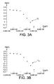
- the figure 3A illustrates, for an example of a device implemented according to the invention and by means of a curve C 1 , the dependence of a voltage Vfg taken on the front face of this device at the level of the thin semi-conducting layer 103 with respect to the potential Vbg on the rear face of this device at the level of the photosensitive zone 205, when the thin semi-conducting layer 103 is based on silicon and has a thickness e 3 of the order of 10 nm, that the insulating layer 101 is a BOX layer of thickness e 2 of the order of 5 nm. With such a device a sensitivity of 260 mV / V can be obtained.
- a curve C 2 illustrates the dependence of the voltage Vfg taken on the front face vis-à-vis the potential Vbg taken on the back, this time for a device with a thin semiconductor layer 103 based on silicon and thickness e 3 of the order of 20 nm, and an insulating layer 101 of BOX of thickness e 2 of the order of 25 nm. With such a device a sensitivity of 350 mV / V can be obtained.
- the figure 4 illustrates a particular detection principle in which a given potential + V generated at the level of the photosensitive zone 205 by light radiation arriving by the face opposite to that where the gate 110 of the transistor T is located, is applied to one of the electrodes of the transistor T, for example the drain electrode 108 to modify its electrical characteristics.
- connection element 150 may be provided for example between the drain and the photosensitive zone.
- transistors T 1 , T 2 , T 3 , T 4 are produced on a semiconductor-on-insulator type substrate, for example of the SOI type (SOI for "Silicon on Insulator” or silicon on insulator).
- SOI SOI for "Silicon on Insulator” or silicon on insulator
- a semiconductor-on-insulator type substrate for example of the SOI type (SOI for "Silicon on Insulator” or silicon on insulator).
- SOI SOI for "Silicon on Insulator” or silicon on insulator
- the transistors T 1 , T 2 , T 3 , T 4 can be produced using a CMOS method and a UTBB type die, that is to say with very thin layers 101a and 102, in particular a lower insulating layer 101a. or equal to 25 nanometers and a thin semiconductor layer 102 less than 10 nanometers.
- the thin insulating layer 101 may be for example a buried silicon oxide layer provided with a thickness e 2 for example less than or equal to 25 nanometers or less than or equal to 10 nanometers.
- the thin semiconductor layer 102 is for its part provided with a thickness e 3 for example between 5 and 10 nanometers, for example of the order of 6 nanometers.
- Some of the transistors T 1 , T 2 , T 3 , T 4 may have different respective threshold voltages V T depending on whether or not they are suitable for photo-detection.
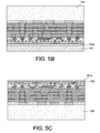
- Several interconnection metal levels M 1 ,..., M k may then be formed in a stack of insulating layers surmounting the transistors T 1 ,..., T 4 ( Figure 5A ).
- a handle layer 120 is formed which may for example be based on a polymer material or another silicon wafer head-to-tail with the CMOS plate.
- the handle layer 120 allows a gripping of the circuit in progress.
- This handle layer 120 may be optionally formed by molecular bonding of a plate on the top of the circuit ( Figure 5B ).
- the sacrificial support layer 100 is removed.
- This removal can be carried out, for example, by a so-called “grinding” or polishing method, in which a flat rotating surface composed of abrasive material removes material 100.
- An etching stop is performed on the thin insulating layer 102 ( Figure 5C ).
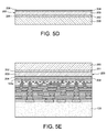
- the photo-sensitive zone 205 may, for its part, be independently formed on another plate or other support on which a photo-detector stack is made.
- This other substrate comprises a support layer 200 covered by an insulating layer 201, for example based on SiO 2 .
- a thin insulating layer 206 which can be for example based on SiO 2 and is intended to serve as a bonding layer ( figure 5D ).
- Bonding for example direct bonding SiO 2 -SiO 2 layer 206 with the thin insulating layer 101a is then carried out in order to assemble the circuit comprising the transistors T 1, ..., T 4 with the photosensitive region 205 ( figure 5E ).
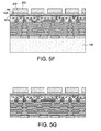
- a withdrawal of the support layer 200 from the photo-detector stack with a stop on the insulating layer 201 can then be performed.
- a stop on the insulating layer 201 preserves all the active layers.
- This insulating layer 201 can then be removed in order to reveal the doped zone 202.
- the image sensor device is thus provided with a plurality of pixels or elementary cells ( figure 5F ).
- a withdrawal of the handle layer 120 can then be performed ( figure 5G ).
- a preliminary cutting of this layer 120 may be provided.
- a transparent material may be deposited before the removal of the handle layer 120.
- the method instead of carrying out the photo-detector stack 202-203-204 with a previously epitaxially-grown PIN type hetero-structure, it is possible to form, for example by gluing, a semiconductor-based layer. undoped conductor and then doping this material, for example by ion implantation, then to anneal the dopants at temperatures compatible with a CMOS process, in order to achieve a PN junction.
- contacts 220a, 220b on each pixel is illustrated, a first contact 220a being provided on the zone 204, a second contact 220b being provided on the area 202 of the photosensitive stack.
- These contacts can be made based on a transparent material such as ITO (ITO for "Indium Tin Oxide").
- contacts common to a set of pixels can also be made.
- transistors T 'of a read circuit are provided between the photo-detector transistors T of the type described above in connection with the Figures 1 to 3 and interconnection metal levels M 1 , ..., M k .
- the figure 8 illustrates experimental results obtained on N-type and P-type transistors having an arrangement of the type of figure 2 , which has been illuminated by the front face with the aid of a polychromatic white light and the evolution of the threshold voltage has been observed
- the transistors made in this example comprise a grid of W width 1.2 ⁇ m, length L of 20 nm, a thickness of the semiconductor layer 102 of 6 nm, a thickness of the insulating layer 101 of 25 nm.
- the semiconductor layer 205 is made of silicon and has an NP junction, arranged so that the zone N is the one located closest to the insulating layer 101.
- the zone P of the layer 205 has been obtained by implanting through the layer isolator 101 and before realization of the transistor, Bore ions at a dose of 3 * 10 13 cm -2 and an energy of 30 keV.
- the zone N of the layer 205 has, in turn, been obtained by implanting through the insulating layer 101 and before making the transistor, As ions at a dose of 4 * 10 13 cm -2 and an energy of between 70 keV and 95 keV.
- the curves C 10 , C 20 and C 30 represent an evolution of the threshold voltage V T of the N type transistor having a zone N of the semiconductor layer 205 implanted with Arsenic in a dose of 4 ⁇ 10 13 cm -2 and for respectively, an energy of 70 keV, 80 keV, and 95 keV, depending on a potential V taken on the rear face of the semiconductor layer 205.
- the curves C 40 , C 50 , C 60 represent an evolution of the threshold voltage V T of the P-type transistor for respectively, a zone N of the semiconductor layer 205 implanted with Arsenic in a 4 * dose. 10 13 cm -2 and respectively for an energy of 70 keV, 80 keV, and 95 keV, depending on a potential V taken on the rear face of the layer 205.
- Curves C 10 , C 20 , C 30 of the figure 8 show that the threshold voltage of the N-type transistor, so its characteristic Id (Vg) (with Id the current flowing through the channel and Vg the gate potential) increases as the illumination increases.
- Curves C 40 , C 50 , C 60 show that the threshold voltage V T of the P-type transistor decreases as illumination increases.
- the threshold voltage offset V T obtained can be of the order of 20 mV to 40 mV in absolute value and depends on the polarization of the rear face of the layer 205.
- the insulating layer 101 based on SiO 2 with a thickness of 5 nm, and a semiconductor layer 102 with a thickness of between 3 nm and 50 nm. nm, advantageously between 3 nm and 25 nm.
- the thickness of the semiconductor layer 102 can be provided between 3 nm and 100 nm, advantageously between 3 nm and 50 nm.
- the operating principle and the ranges of thicknesses mentioned above remain valid even when the material of the insulating layer 101 is not based on silicon oxide, but on an insulating material, such as, for example, nitride silicon, or hafnium oxide.
Abstract
Description
- La présente invention se rapporte au domaine de la photo-détection et de l'imagerie et concerne la mise en oeuvre d'un dispositif imageur amélioré en termes d'agencement et doté d'un élément de photo-détection et d'un élément de lecture associés dans lequel la transmission de signal entre l'élément de détection et l'élément de lecture est simplifiée.
- Un dispositif capteur d'image peut être formé d'une matrice d'éléments photo-détecteurs connectée et assemblée avec un circuit électronique de lecture par des éléments de connexion. Selon un exemple de réalisation connu, ces éléments de connexion peuvent être des billes d'Indium. Un tel assemblage nécessite un alignement précis entre le circuit de lecture et les éléments photo-détecteurs et pose des problèmes d'encombrement.
- Dans un dispositif capteur d'image de type CMOS, les pixels sont généralement formés d'un élément photo-détecteur tel qu'une photodiode par exemple de type communément appelée « pinned », et d'un élément de lecture, par exemple sous forme d'un convertisseur de charge/tension.
- Un exemple de capteur d'image CMOS est donné dans le document
US 6 967 120 B2 et comporte un transistor de lecture dont la grille est accolée à la photodiode, le transistor étant réalisé sur une même face d'un substrat que la photodiode. - Dans ce type de dispositif, le transistor de lecture est utilisé pour collecter des électrons excédentaires générés par la lumière détectée. Pendant ce transfert, une partie des électrons peut se recombiner, ce qui diminue le rendement de collection.
- Dans un tel capteur, le transistor de lecture occupe par ailleurs sur le substrat un espace qui n'est pas directement utilisé pour la conversion de la lumière en électrons.
- Le document
WO 2006/043105 A1 présente un dispositif capteur d'image comprenant un transistor de lecture reposant sur un substrat semi-conducteur sur isolant, le substrat comportant une couche de support semi-conductrice dans laquelle une jonction est réalisée et qui permet de produire des charges lorsque la couche de support est illuminée. Des charges générées au niveau de cette jonction sont collectées par le biais d'une interconnexion métallique prévue entre le transistor de lecture et la jonction. - Le document
US 4 954 895 présente quant à lui un dispositif capteur d'image doté d'un premier transistor dont le canal est situé dans une couche semi-conductrice dopée P reposant sur une couche semi-conductrice dopée N avec laquelle elle réalise une jonction. Lorsque cette jonction est illuminée, des charges sont produites, collectées au niveau du drain du premier transistor et transmises à un transistor de commutation dont la zone de drain vient en contact avec celle du premier transistor. - Il se pose le problème de mettre en oeuvre une nouvelle structure de capteur d'image améliorée vis-à-vis des inconvénients évoqués ci-dessus, notamment en termes d'encombrement.
- La présente invention prévoit tout d'abord un dispositif capteur d'image comprenant au moins un transistor reposant sur un substrat comprenant une fine couche semi-conductrice dans laquelle une zone de canal dudit transistor est prévue, une couche isolante séparant la fine couche semi-conductrice d'une couche de support semi-conductrice, la couche de support semi-conductrice comprenant au moins une zone de photo-détection comportant au moins une région dopée P et au moins une région dopée N formant une jonction, la jonction étant disposée en regard de la zone de canal dudit transistor.
- Le matériau à base duquel la couche isolante est formée, ainsi que l'épaisseur cette couche isolante, sont prévues de sorte qu'un couplage capacitif peut être établi entre la zone de photo-détection et la zone de canal dudit transistor.
- Ainsi, un rayonnement lumineux incident sur la zone de photo-détection engendre un signal de détection transmis par couplage capacitif audit transistor.
- Un tel dispositif a un agencement amélioré et en particulier un encombrement limité par rapport aux dispositifs dans lequel un transistor de lecture et une zone de photo-détection sont juxtaposés.
- Par rapport à un dispositif suivant l'art antérieur dans lequel un transistor de lecture et une zone de photo-détection sont juxtaposés, le dispositif suivant l'invention permet, pour un substrat de même taille, de dédier une surface plus importante à la photo-détection.
- Avec un dispositif suivant l'invention toute la surface de la zone photosensible sur laquelle repose le transistor peut être utilisée pour réaliser une détection de rayonnement lumineux, contrairement à un capteur CMOS suivant l'art antérieur pour lequel une partie d'un élément de détection élémentaire est généralement occupée par au moins un transistor de lecture.
- Dans le dispositif suivant l'invention, une connectique dédiée entre la zone photosensible et un transistor de lecture n'est pas nécessaire, ce qui peut faciliter notamment la réalisation du dispositif et en particulier permet de s'affranchir de problèmes d'état de surface, de décollement, de contrainte mécanique.
- Ainsi, le dispositif peut être prévu de sorte que le transistor et la zone photosensible sont couplés mais ne sont pas reliés par le biais d'une connexion électrique. Dans ce cas, la portion de couche isolante séparant le transistor et la zone sensible est continue, sans qu'un élément de connexion ne la traverse.
- Selon l'invention, un rayonnement lumineux incident sur la zone de photo-détection induit un changement de la tension de seuil dudit transistor.
- Pour cela, la couche isolante peut être prévue avec une épaisseur qui peut être inférieure ou égale à 25 nanomètres ou inférieure ou égale à 10 nanomètres.
- La fine couche semi-conductrice peut avoir quant à elle une épaisseur inférieure à 800 nm et avantageusement entre 5 nm et 100 nm.
- La zone de photo-détection peut avoir une épaisseur inférieure à 1 micromètre.
- Selon une possibilité de mise en oeuvre, la jonction est une jonction P-I-N.
- Une jonction PIN permet d'obtenir une zone de charge d'espace d'épaisseur plus importante et ainsi d'augmenter l'épaisseur de la zone de collection efficace des photons. Quand les photons sont absorbés dans l'épaisseur correspondant à cette zone de charge d'espace, les paires électrons-trous photo-générées sont efficacement dissociés, ce qui maximise la tension induite aux bornes de la photodiode.
- La zone photosensible et la fine couche semi-conductrice peuvent être à base de matériaux semi-conducteurs différents. Le matériau constituant la couche de photo-détection peut être ainsi choisi en fonction de la longueur d'onde à détecter, tandis que le matériau dans lequel la zone de canal du transistor est réalisée est choisi de manière à permettre de conférer à ce dernier des performances électriques optimales.
- Selon un autre aspect, la présente invention concerne également un procédé de réalisation d'un dispositif capteur d'image comprenant des étapes de :
- réalisation d'un transistor reposant sur un substrat, le substrat comprenant une couche isolante et une fine couche semi-conductrice dans laquelle une zone de canal dudit transistor est réalisée,
- assemblage d'une couche de support semi-conductrice destinée à former une zone de photo-détection comprenant une jonction en regard de la zone de canal dudit transistor.
- Un tel assemblage peut être réalisé sans nécessiter un alignement précis.
- Un tel assemblage permet de mettre en oeuvre un dispositif capteur d'image comprenant une couche de support dopée préalablement et éventuellement de mettre en oeuvre une couche de support à base d'un matériau différent de celui de la fine couche semi-conductrice dans laquelle le canal du transistor est réalisé.
- Un tel assemblage permet également de mettre en oeuvre un dispositif capteur d'image comprenant une couche de support d'épaisseur réduite.
- Le matériau à base duquel la couche isolante est formée, ainsi que l'épaisseur cette couche isolante, sont prévues de sorte qu'un couplage capacitif peut être établi entre la zone de photo-détection et la zone de canal dudit transistor.
- L'assemblage peut être effectué par collage moléculaire de la couche isolante avec une autre couche isolante recouvrant ladite couche de support.
- Un tel assemblage permet de mettre en oeuvre une zone de photo-détection à base de matériaux semi-conducteurs tels que l'InGaAs, ou l'InSb, ou le GaN, ou le CdHgTe, et qui contrairement à un matériau semi-conducteur tel que le Si sont difficiles à mettre sous forme de plaques de tailles importantes.
- La présente invention sera mieux comprise à la lecture de la description d'exemples de réalisation donnés, à titre purement indicatif et nullement limitatif, en faisant référence aux dessins annexés sur lesquels :
- la
figure 1 illustre un exemple de dispositif capteur d'image suivant l'invention doté d'une zone photosensible comportant une jonction disposée en regard du canal d'un transistor de détection reposant sur une couche isolante, - la
figure 2 illustre un exemple de dispositif capteur d'image suivant l'invention, doté d'une zone photosensible comprenant une jonction PIN, - les
figures 3A-3B illustrent un phénomène de couplage dans un dispositif capteur d'image suivant l'invention, entre une zone photosensible et une zone semi-conductrice de canal d'un transistor de détection, - la
figure 4 illustre un exemple de dispositif capteur d'image suivant l'invention, doté d'un transistor de détection dont une électrode est mise au potentiel d'une zone photosensible disposée en regard dudit transistor, - les
figures 5A-5H illustrent un exemple de procédé de réalisation d'un dispositif capteur d'image suivant l'invention comportant au moins une zone photosensible disposée en regard du canal d'au moins un transistor de détection reposant sur une couche isolante, - la
figure 6 illustre un exemple de dispositif capteur d'image suivant l'invention doté de zones de contact qui peuvent être à base d'ITO, - la
figure 7 illustre un exemple de dispositif capteur d'image suivant l'invention doté de transistors d'un circuit de lecture placés dans un empilement entre des transistors de détection du type de celui donné sur lesfigures 1 à 3 , et des niveaux métalliques d'interconnexion, - La
figure 8 illustre une variation de tension de seuil sur des transistors de type N et de type P ayant un agencement du type de celui de lafigure 2 et soumis à un éclairement variable. - Des parties identiques, similaires ou équivalentes des différentes figures portent les mêmes références numériques de façon à faciliter le passage d'une figure à l'autre.
- Les différentes parties représentées sur les figures ne le sont pas nécessairement selon une échelle uniforme, pour rendre les figures plus lisibles.
- Un exemple de cellule élémentaire également appelée « pixel » d'un dispositif capteur d'image suivant l'invention va à présent être décrit en liaison avec les
figures 1, 2 et3 . - Ce pixel comprend une zone photo-sensible 205 formée d'au moins deux zones dopées superposées réalisant une jonction de diode, par exemple une jonction de type PN.
- L'épaisseur e1 de la zone photosensible et exposée au rayonnement, peut être prévue supérieure à 1/a, a étant le coefficient d'absorption linéique du matériau de la zone photosensible, ceci afin de maximiser les absorptions de photons dans la partie photosensible, et en particulier dans la zone de charge d'espace.
- L'épaisseur e1 de la zone photosensible peut être par exemple comprise entre 100 nm et 10 µm par exemple de l'ordre de 1 µm.
- La zone photo-détectrice peut avoir une surface par exemple de l'ordre du µm2 pour une détection de longueur d'onde par exemple de l'ordre du micromètre.
- Dans l'exemple donné sur la
figure 2 , la zone photosensible 205 est sous forme d'une diode PIN et comprend une première zone 202 dopée selon un dopage d'un premier type, par exemple de type N, qui peut être dévoilée ou découverte. - La première zone dopée 202 a une épaisseur e11 qui peut être prévue inférieure à 1/a et par exemple comprise entre 2 nm et 200 nm ou de l'ordre de 100 nanomètres.
- La première zone dopée 202 est surmontée d'une zone semi-conductrice intrinsèque 203 ou non dopée, ayant une épaisseur e12 qui peut être comprise par exemple entre 100 nm et un ou plusieurs microns, elle-même surmontée d'une deuxième zone dopée 204 selon un dopage d'un deuxième type, par exemple de type P. La deuxième zone dopée 204 a, quant à elle, une épaisseur e13 qui peut être comprise par exemple entre 100 nm et 1 µm.
- La zone photosensible 205 est à base d'un matériau choisi en fonction de la longueur d'onde ou de la gamme de longueurs d'ondes que l'on souhaite détecter. La zone photosensible 205 peut être formée par exemple d'un ou plusieurs matériau(x) semi-conducteur(s) parmi les matériaux suivants : Si, Ge, InGaAs, InSb, CdHgTe, GaN.
- Dans un cas, par exemple, où le capteur est prévu pour détecter un rayonnement situé dans le domaine UV, le matériau de la zone photosensible 205 peut être un matériau semi-conducteur III-V, par exemple à base de GaN ou d'AlGaN.
- Dans un autre cas, par exemple, où le capteur est destiné à détecter un rayonnement ayant une longueur d'onde dans une gamme inférieure à 1.1 µm, la zone photosensible peut être par exemple à base de silicium.
- Si l'on souhaite détecter un rayonnement ayant une longueur d'onde dans une gamme comprise entre 1.3 µm et 1.55 µm, le matériau de la zone photosensible peut être par exemple prévu à base de Germanium ou d'un matériau III-V tel que de l'InGaAs.
- Selon un autre exemple, pour détecter un rayonnement ayant une longueur d'onde dans une gamme comprise entre 3 µm et 5 µm ou entre 8 µm et 12 µm, un matériau II-VI, par exemple à base de CdHgTe peut être utilisé.
- La zone photosensible 205 forme ainsi une couche de support d'un substrat de type semi-conducteur sur isolant et est surmontée par une fine couche isolante 101. Cette fine couche isolante 101 peut être par exemple à base de SiO2. La fine couche isolante 101 peut être prévue avec une épaisseur e2 choisie suffisamment faible pour qu'une tension photo-générée sur sa face arrière puisse induire une tension correspondante par phénomène de couplage capacitif sur sa face avant.
- L'épaisseur e2max maximale de la fine couche isolante 101, peut être en particulier prévue de manière à permettre un couplage capacitif entre la zone photosensible 205 et une fine couche semi-conductrice 102 en contact avec cette dernière. L'épaisseur e2 de la fine couche isolante est de préférence inférieure à 300 nm et comprise par exemple entre 2 nm et 300 nm, par exemple inférieure ou égale à 25 nanomètres ou inférieure ou égale à 10 nanomètres.
- A titre d'exemple, une variation de tension de seuil du transistor T peut être de l'ordre de 80 mV lorsqu'on applique un potentiel de 1V sur la face arrière avec une couche isolante 101 à base de SiO2 d'épaisseur e2 de l'ordre de 25 nm et une fine couche semi-conductrice 102 de silicium de 7 nm.
- La fine couche semi-conductrice 103 surmontant la couche isolante 101 peut quant à elle être prévue avec une épaisseur e3 inférieure à 800 nm correspondant à l'épaisseur de déplétion d'un substrat non dopé pour une tension de grille de 0V, et en particulier comprise par exemple entre 5 nm et 100 nanomètres. Une épaisseur inférieure à 100 nm permet d'obtenir une couche complètement déplétée.
- La mise en oeuvre de couches semi-conductrices 103 et 205 et d'une couche isolante 101 de faibles épaisseurs peut permettre de réaliser un capteur d'image avec une épaisseur totale suffisamment faible pour qu'il soit flexible.
- Dans la fine couche semi-conductrice 102, une zone de canal 104 d'un transistor T est formée. La fine couche 102 peut être à base d'un matériau semi-conducteur différent de celui de la zone photosensible.
- La fine couche 102 peut être, par exemple, à base de silicium, tandis que la zone photosensible 205 est formée d'un autre matériau semi-conducteur choisi en fonction du rayonnement lumineux à détecter. Le canal du transistor T peut être complètement déserté. Le transistor T ainsi réalisé peut être de type UTBB (UTBB pour « Ultra Thin BOX and Body »).
- Ce transistor comporte en outre une zone de diélectrique 109 de grille, ainsi qu'une électrode de grille 110 reposant sur la zone diélectrique 109.
- La zone de canal 104 et la grille 110 du transistor T sont situées en regard d'une région de la zone photosensible 205. Dans le cas, par exemple, où la grille 110 a une dimension critique ou une longueur par exemple de l'ordre de 30 nm, la fine couche semi-conductrice 102 peut être prévue par exemple entre 5 nanomètres et 7 nanomètres.
- La grille 110 est entourée de part et d'autre de zones isolantes formant des premiers espaceurs 112. Les premiers espaceurs 112 sont partiellement enterrés dans la zone active du transistor T et en contact avec des flancs de la grille 110, tandis que d'autres zones isolantes formant des deuxièmes espaceurs 114, reposent sur la zone active du transistor T et sont disposés contre les premiers espaceurs 112.
- Lorsque la zone photo-sensible 205 ou photo-détectrice est soumise au rayonnement lumineux R, cela peut entrainer une modification de la tension de seuil VT du transistor T, l'amplitude de cette modification pouvant permettre de traduire une détection d'un flux donné de photons associé à ce rayonnement lumineux. Une détection de certains rayonnements lumineux pénétrant par la face avant du dispositif, c'est-à-dire la face où se situe la grille 110, est possible.
- Un circuit de lecture peut par exemple être mis en oeuvre au niveau du ou des transistors servant à la détection. Les transistors du circuit de lecture sont de préférence prévus de sorte que leur tension de seuil, contrairement au transistor T, soit insensible au flux lumineux. Pour ce faire, on peut par exemple, mettre en oeuvre ces transistors du circuit de lecture de sorte qu'ils aient une couche isolante 101 plus épaisse ou alors une épaisseur de canal plus importante ou un dopage qui ne le rende pas complètement déserté.
- Selon une possibilité de mise en oeuvre, un mode de détection binaire peut être réalisé avec un capteur suivant l'invention. Ainsi, le dispositif capteur d'image peut être prévu pour que, lorsqu'il n'y a pas de rayonnement lumineux à détecter, la tension de seuil VT du transistor T est égale à une valeur Vt1.
- Lorsque le capteur reçoit un rayonnement lumineux R, une modification de la polarisation du transistor au niveau de son plan de masse induit une modification de la tension de seuil du transistor égale à une autre valeur Vt2 = Vt1 + ΔVt ou Vt2 = Vt1 - ΔVt, avec ΔVt non nul.
- Le transistor peut donc être en état bloqué également appelé « OFF » lorsqu'il n'y a pas de flux de photons à détecter et en état passant ou « ON » lorsqu'il y a un flux de photons à détecter.
- Lorsque le dispositif capteur d'image est en fonctionnement, les tensions de polarisation VD et VG respectivement prévues sur la zone de drain et sur la grille du transistor T peuvent être de l'ordre du volt.
- La
figure 3A illustre, pour un exemple de dispositif mis en oeuvre suivant l'invention et par l'intermédiaire d'une courbe C1, la dépendance d'une tension Vfg prise en face avant de ce dispositif au niveau de la fine couche semi-conductrice 103 vis-à-vis du potentiel Vbg en face arrière de ce dispositif au niveau de la zone photosensible 205, lorsque la fine couche semi-conductrice 103 est à base de silicium et a une épaisseur e3 de l'ordre de 10 nm, que la couche isolante 101 est une couche de BOX d'épaisseur e2 de l'ordre de 5 nm. Avec un tel dispositif une sensibilité de 260 mV/V peut être obtenue. - Sur la
figure 3B une courbe C2 illustre la dépendance de la tension Vfg prise en face avant vis-à-vis du potentiel Vbg pris en face arrière, cette fois pour un dispositif doté d'une fine couche semi-conductrice 103 à base de silicium et d'épaisseur e3 de l'ordre de 20nm, et une couche isolante 101 de BOX d'épaisseur e2 de l'ordre de 25 nm. Avec un tel dispositif une sensibilité de 350 mV/V peut être obtenue. - La
figure 4 illustre un principe de détection particulier dans lequel un potentiel donné +V généré au niveau de la zone photosensible 205 par un rayonnement lumineux arrivant par la face opposée à celle où se trouve la grille 110 du transistor T, est appliqué à l'une des électrodes du transistor T, par exemple l'électrode de drain 108 pour en modifier ses caractéristiques électriques. - Pour ce mode de réalisation, un élément de connexion 150 peut être prévu par exemple entre le drain et la zone photosensible.
- Un procédé de réalisation d'un dispositif capteur d'image suivant l'invention, va à présent être décrit en liaison avec les
figures 5A-5H . - On réalise tout d'abord un ou plusieurs transistors T1, T2, T3, T4 sur un substrat de type semi-conducteur sur isolant, par exemple de type SOI (SOI pour « Silicon on Insulator » ou silicium sur isolant) comprenant une couche de support 100 sacrificielle, une fine couche isolante 101a reposant sur la couche de support 100, et une fine couche semi-conductrice 102 reposant sur la couche isolante 101a.
- Les transistors T1, T2, T3, T4 peuvent être réalisés selon un procédé CMOS et une filière de type UTBB, c'est à dire avec des couches 101a et 102 de très faible épaisseur, en particulier une couche isolante 101a inférieure ou égale à 25 nanomètres et une fine couche semi-conductrice 102 inférieure à 10 nanomètres.
- La fine couche isolante 101, peut être par exemple une couche d'oxyde de silicium enterrée prévue avec une épaisseur e2 comprise par exemple inférieure ou égale à 25 nanomètres ou inférieure ou égale à 10 nanomètres. La fine couche semi-conductrice 102 est quant à elle prévue avec une épaisseur e3 comprise par exemple entre 5 et 10 nanomètres, par exemple de l'ordre de 6 nanomètres.
- Certains des transistors T1, T2, T3, T4, peuvent avoir des tensions de seuil VT respectives différentes suivant qu'ils sont ou non adaptés à la photo-détection. Plusieurs niveaux M1,..., Mk métalliques d'interconnexion peuvent être ensuite formés dans un empilement de couches isolantes surmontant les transistors T1,...,T4 (
figure 5A ). - Ensuite, on forme une couche poignée 120 qui peut être par exemple à base d'un matériau polymère ou une autre plaque de silicium collée tête bêche avec la plaque CMOS. La couche poignée 120 permet une préhension du circuit en cours de réalisation. Cette couche poignée 120 peut être éventuellement formée par collage moléculaire d'une plaque sur le dessus du circuit (
figure 5B ). - Ensuite, on effectue un retrait de la couche de support sacrificielle 100. Ce retrait peut être réalisé par exemple par un procédé de polissage communément appelé de « grinding » ou rodage, dans lequel une surface plane en rotation composée de matériau abrasif retire du matériau 100 de manière mécanique, et par une gravure chimique par exemple à base de TMAH (TMAH pour « tetra-methyl ammonium hydroxide ») en particulier lorsque la couche de support 100 sacrificielle est à base de Si. Un arrêt de gravure est réalisé sur la fine couche isolante 102 (
figure 5C ). - La zone photo-sensible 205 peut, quant à elle, être formée indépendamment sur une autre plaque ou un autre support sur lequel un empilement photo-détecteur est réalisé. Un empilement formé par exemple d'une couche 202 de Ge dopé N recouverte par, et en contact avec, une couche 203 de Ge non dopé, cette couche 203 étant recouverte et en contact avec, une couche 204 de Ge dopé P en pleine plaque sur un substrat de type GeOl, peut être réalisé. Cet autre substrat comprend une couche de support 200 recouvert par une couche isolante 201, par exemple à base de SiO2. Après avoir réalisé la couche 204 de Ge dopé P, on peut former, par exemple par dépôt, une fine couche isolante 206, qui peut être par exemple à base de SiO2 et est destinée à servir de couche de collage (
figure 5D ). - Un collage, par exemple un collage direct SiO2-SiO2 de la couche 206 avec la fine couche isolante 101a est ensuite réalisé afin d'assembler le circuit comprenant les transistors T1,...,T4 avec la zone photosensible 205 (
figure 5E ). - Un retrait de la couche de support 200 de l'empilement photo-détecteur avec arrêt sur la couche isolante 201 peut être ensuite effectué. Un arrêt sur la couche isolante 201 permet de préserver toutes les couches actives. Cette couche isolante 201 peut être ensuite retirée afin de dévoiler la zone dopée 202.
- Ensuite, on peut effectuer une gravure de la zone photosensible afin de former plusieurs zones photosensibles distinctes correspondant chacune à une cellule élémentaire ou à un pixel. Une délimitation géométrique des pixels ou cellules du dispositif capteur d'image est ainsi réalisée. Le dispositif capteur d'image est ainsi prévu avec une pluralité de pixels ou de cellules élémentaires (
figure 5F ). - Un retrait de la couche poignée 120 peut être ensuite effectué (
figure 5G ). Afin de faciliter ce retrait, une découpe préalable de cette couche 120 peut être prévue. - Dans le cas où l'épaisseur totale du capteur d'image est faible, on peut éventuellement déposer un matériau transparent avant le retrait de la couche poignée 120.
- Puis, on peut réaliser un test du dispositif capteur d'image (
figure 5H ). Selon une variante de réalisation du procédé, au lieu de réaliser l'empilement 202-203-204 photo-détecteur avec une hétéro-structure de type P-I-N préalablement épitaxiée, on peut former par exemple par collage, une couche à base de matériau semi-conducteur non dopé et doper ensuite ce matériau, par exemple par implantation ionique, puis de réaliser un recuit des dopants à des températures compatibles avec un procédé CMOS, ce afin de réaliser une jonction P-N. - Sur la
figure 6 , une réalisation de contacts 220a, 220b sur chaque pixel est illustrée, un premier contact 220a étant prévu sur la zone 204, un deuxième contact 220b étant prévu sur la zone 202 de l'empilement photosensible. Ces contacts peuvent être réalisés à base d'un matériau transparent tel que de l'ITO (ITO pour « Indium Tin Oxide »). - Selon une autre variante (non représentée), des contacts communs à un ensemble de pixels peuvent être également réalisés.
- Sur la
figure 7 un autre exemple de dispositif microélectronique détecteur de rayonnement lumineux suivant l'invention est donné. - Dans cet exemple, des transistors T' d'un circuit de lecture sont prévus entre les transistors photo-détecteurs T du type de celui décrit précédemment en liaison avec les
figures 1 à 3 et des niveaux métalliques d'interconnexion M1,...,Mk. - La
figure 8 illustre des résultats expérimentaux obtenus sur des transistors de type N et de type P ayant un agencement du type de celui de lafigure 2 , que l'on a illuminé par la face avant à l'aide d'une lumière blanche polychromatique et dont on a observé l'évolution de la tension de seuil - Les transistors réalisés dans cet exemple comportent une grille de largeur W de 1,2 µm, de longueur L de 20 nm, une épaisseur de la couche semi-conductrice 102 de 6 nm, une épaisseur de la couche isolante 101 de 25 nm. La couche semi-conductrice 205 est en silicium et comporte une jonction N-P, agencée de sorte que la zone N est celle située la plus proche de la couche isolante 101. La zone P de la couche 205 a été obtenue en implantant à travers la couche isolante 101 et avant réalisation du transistor, des ions Bore à une dose de 3*1013 cm-2 et une énergie de 30 keV.
- La zone N de la couche 205 a, quant à elle, été obtenue en implantant à travers la couche isolante 101 et avant réalisation du transistor, des ions As à une dose de 4*1013 cm-2 et une énergie comprise entre 70 keV et 95 keV.
- Sur la
figure 8 , les courbes C10, C20, C30 représentent une évolution de la tension de seuil VT du transistor de type N ayant une zone N de la couche semi-conductrice 205 implantée avec de l'Arsenic selon une dose de 4*1013 cm-2 et pour respectivement, une énergie de 70 keV, de 80 keV, et de 95 keV, en fonction d'un potentiel V pris sur la face arrière de la couche semi-conductrice 205. - Les courbes C40, C50, C60 représentent une évolution de la tension de seuil VT du transistor de type P pour respectivement, une zone N de la couche semi-conductrice 205 implantée avec de l'Arsenic selon une dose de 4*1013 cm-2 et respectivement pour une énergie de 70 keV, de 80 keV, et de 95 keV, en fonction d'un potentiel V pris sur la face arrière de la couche 205.
- Les courbes C10, C20, C30 de la
figure 8 montrent que la tension de seuil du transistor de type N, donc sa caractéristique Id(Vg) (avec Id le courant parcourant le canal et Vg le potentiel de grille) augmente lorsque l'éclairement augmente. - Les courbes C40, C50, C60 montrent que la tension de seuil VT du transistor de type P diminue lorsque l'éclairement augmente.
- Le décalage de tension de seuil VT obtenu peut être de l'ordre de 20 mV à 40 mV en valeur absolue et dépend de la polarisation de la face arrière de la couche 205.
- En adaptant le couple épaisseur de la couche semi-conductrice 102/épaisseur de la couche isolante 101, un décalage de tension de seuil plus important peut être obtenu.
- Pour obtenir une sensibilité de couplage supérieure à 50 mV/V, on peut prévoir par exemple la couche isolante 101 à base de SiO2 avec une épaisseur de 5 nm, et une couche semi-conductrice 102 avec une épaisseur comprise entre 3 nm à 50 nm, avantageusement entre 3 nm et 25 nm.
- Pour une épaisseur de couche isolante 101 de 10 nm, on peut prévoir l'épaisseur de la couche semi-conductrice 102 entre 3 nm et 100 nm, avantageusement comprise entre 3 nm à 50 nm.
- Le principe de fonctionnement et les gammes d'épaisseurs mentionnées ci-dessus restent valident pour une zone de canal à base d'un autre matériau semi-conducteur que le silicium, par exemple pour une zone de canal à base de siliciure de germanium.
- Le principe de fonctionnement et les gammes d'épaisseurs mentionnées ci-dessus restent valables même lorsque le matériau de la couche isolante 101 n'est pas à base d'oxyde de silicium, mais d'un matériau isolant, tel que par exemple du nitrure de silicium, ou de l'oxyde d'hafnium.
Claims (11)
- Dispositif capteur d'image comprenant au moins un transistor reposant sur un substrat semi-conducteur sur isolant, le substrat comprenant une fine couche semi-conductrice dans laquelle une zone de canal dudit transistor est réalisée, une couche isolante séparant la fine couche semi-conductrice avec une couche de support semi-conductrice, le dispositif étant caractérisé en ce que la couche de support semi-conductrice comprend au moins une zone photosensible comportant au moins une région dopée P et au moins une région dopée N formant une jonction disposée en regard de la zone de canal dudit transistor, la couche isolante ayant une composition et une épaisseur prévues de manière à permettre un couplage capacitif entre la zone photosensible et la fine couche semi-conductrice.
- Dispositif selon la revendication 1, dans lequel la jonction est une jonction P-I-N.
- Dispositif selon l'une des revendications 1 ou 2, dans lequel la couche isolante a une épaisseur inférieure ou égale à 25 nanomètres.
- Dispositif selon l'une des revendications 1 à 3, dans lequel la fine couche semi-conductrice a une épaisseur inférieure à 800 nm et avantageusement comprise entre 5 nm et 100 nm.
- Dispositif selon l'une des revendications 1 à 4, dans lequel la zone photosensible a une épaisseur supérieure à 1/a, a étant le coefficient d'absorption linéique du matériau de la zone photosensible.
- Dispositif selon l'une des revendications 1 à 5, dans lequel la zone photosensible et la fine couche semi-conductrice sont à base de matériaux semi-conducteurs différents.
- Procédé de réalisation d'un dispositif capteur d'image comprenant des étapes de :- réalisation d'un transistor reposant sur un substrat, le substrat comprenant une couche isolante et une fine couche semi-conductrice dans laquelle une zone de canal dudit transistor est réalisée,- assemblage d'une couche de support semi-conductrice destinée à former une zone de photosensible comprenant une jonction en regard de la zone de canal dudit transistor.
- Procédé selon la revendication 7, dans lequel l'assemblage est réalisé par collage de la couche isolante avec une autre couche isolante recouvrant ladite couche de support.
- Procédé selon la revendication 7 ou 8, la jonction étant une jonction PIN.
- Procédé selon l'une des revendications 7 à 9, dans lequel la zone photosensible et la fine couche semi-conductrice sont à base de matériaux semi-conducteurs différents.
- Procédé selon l'une des revendications 7 à 10, la couche isolante ayant une composition et une épaisseur prévues de manière à permettre un couplage capacitif entre la zone photosensible et la fine couche semi-conductrice.
Applications Claiming Priority (1)
| Application Number | Priority Date | Filing Date | Title |
|---|---|---|---|
| FR1159802A FR2982079A1 (fr) | 2011-10-28 | 2011-10-28 | Imageur cmos utbb |
Publications (2)
| Publication Number | Publication Date |
|---|---|
| EP2587539A1 true EP2587539A1 (fr) | 2013-05-01 |
| EP2587539B1 EP2587539B1 (fr) | 2014-07-16 |
Family
ID=47040603
Family Applications (1)
| Application Number | Title | Priority Date | Filing Date |
|---|---|---|---|
| EP12190041.9A Active EP2587539B1 (fr) | 2011-10-28 | 2012-10-25 | Imageur CMOS UTBB |
Country Status (3)
| Country | Link |
|---|---|
| US (1) | US8890219B2 (fr) |
| EP (1) | EP2587539B1 (fr) |
| FR (1) | FR2982079A1 (fr) |
Cited By (3)
| Publication number | Priority date | Publication date | Assignee | Title |
|---|---|---|---|---|
| FR3021458A1 (fr) * | 2014-05-23 | 2015-11-27 | Commissariat Energie Atomique | Inverseur cmos photonique |
| EP3163622A1 (fr) * | 2015-10-28 | 2017-05-03 | Commissariat À L'Énergie Atomique Et Aux Énergies Alternatives | Cellule logique photosensible a illumination par la face avant |
| FR3070792A1 (fr) * | 2017-09-05 | 2019-03-08 | Commissariat A L'energie Atomique Et Aux Energies Alternatives | Detecteur photosensible a jonction 3d et grille autoalignees |
Families Citing this family (6)
| Publication number | Priority date | Publication date | Assignee | Title |
|---|---|---|---|---|
| KR102191327B1 (ko) * | 2014-01-14 | 2020-12-15 | 삼성전자주식회사 | 단위 픽셀 및 이를 포함하는 이미지 픽셀 어레이 |
| US10295983B2 (en) | 2017-10-05 | 2019-05-21 | International Business Machines Corporation | Process-specific views of large frame pages with variable granularity |
| US10158039B1 (en) | 2017-10-16 | 2018-12-18 | International Business Machines Corporation | Heterojunction diode having a narrow bandgap semiconductor |
| CN108666336B (zh) * | 2018-05-29 | 2020-09-11 | 北京大学 | 一种utbb光电探测器阵列及其工作方法 |
| CN111063702B (zh) * | 2019-11-13 | 2022-10-04 | 北京大学 | 一种utbb光电探测器像素单元、阵列和方法 |
| CN112584068B (zh) * | 2020-11-06 | 2022-04-05 | 北京大学 | 一种像素单元和像素单元的信号处理方法 |
Citations (5)
| Publication number | Priority date | Publication date | Assignee | Title |
|---|---|---|---|---|
| US4954895A (en) | 1987-12-04 | 1990-09-04 | Hitachi, Ltd. | Solid-state imaging device including photoelectric conversion elements integrated at a surface of a semiconductor substrate |
| US6967120B2 (en) | 2002-07-19 | 2005-11-22 | Dongbu Anam Semiconductor | Pinned photodiode for a CMOS image sensor and fabricating method thereof |
| WO2006043105A1 (fr) | 2004-10-23 | 2006-04-27 | The Queen's University Of Belfast | Dispositif electro-optique |
| US20060125038A1 (en) * | 2004-12-15 | 2006-06-15 | Sony Corporation | Back-illuminated type solid-state imaging device |
| WO2007001146A1 (fr) * | 2005-06-28 | 2007-01-04 | Siliconfile Technologies Inc. | Pixel d'unite de type separation 3d destine a un capteur d'image et son procede de production |
Family Cites Families (4)
| Publication number | Priority date | Publication date | Assignee | Title |
|---|---|---|---|---|
| US7271025B2 (en) * | 2005-07-12 | 2007-09-18 | Micron Technology, Inc. | Image sensor with SOI substrate |
| US20070218579A1 (en) * | 2006-03-17 | 2007-09-20 | Sharp Laboratories Of America, Inc. | Wide output swing CMOS imager |
| US8035806B2 (en) * | 2008-05-13 | 2011-10-11 | Samsung Electronics Co., Ltd. | Distance measuring sensor including double transfer gate and three dimensional color image sensor including the distance measuring sensor |
| US9054221B2 (en) * | 2011-08-31 | 2015-06-09 | Institute of Microelectronics, Chinese Academy of Sciences | Semiconductor device with a common back gate isolation region and method for manufacturing the same |
-
2011
- 2011-10-28 FR FR1159802A patent/FR2982079A1/fr not_active Withdrawn
-
2012
- 2012-10-25 EP EP12190041.9A patent/EP2587539B1/fr active Active
- 2012-10-26 US US13/661,418 patent/US8890219B2/en active Active
Patent Citations (5)
| Publication number | Priority date | Publication date | Assignee | Title |
|---|---|---|---|---|
| US4954895A (en) | 1987-12-04 | 1990-09-04 | Hitachi, Ltd. | Solid-state imaging device including photoelectric conversion elements integrated at a surface of a semiconductor substrate |
| US6967120B2 (en) | 2002-07-19 | 2005-11-22 | Dongbu Anam Semiconductor | Pinned photodiode for a CMOS image sensor and fabricating method thereof |
| WO2006043105A1 (fr) | 2004-10-23 | 2006-04-27 | The Queen's University Of Belfast | Dispositif electro-optique |
| US20060125038A1 (en) * | 2004-12-15 | 2006-06-15 | Sony Corporation | Back-illuminated type solid-state imaging device |
| WO2007001146A1 (fr) * | 2005-06-28 | 2007-01-04 | Siliconfile Technologies Inc. | Pixel d'unite de type separation 3d destine a un capteur d'image et son procede de production |
Cited By (9)
| Publication number | Priority date | Publication date | Assignee | Title |
|---|---|---|---|---|
| FR3021458A1 (fr) * | 2014-05-23 | 2015-11-27 | Commissariat Energie Atomique | Inverseur cmos photonique |
| EP2947689A3 (fr) * | 2014-05-23 | 2016-02-24 | Commissariat à l'Énergie Atomique et aux Énergies Alternatives | Inverseur cmos photonique |
| US9841657B2 (en) | 2014-05-23 | 2017-12-12 | Commissariat à l'énergie atomique et aux énergies alternatives | CMOS photonic inverter |
| EP3163622A1 (fr) * | 2015-10-28 | 2017-05-03 | Commissariat À L'Énergie Atomique Et Aux Énergies Alternatives | Cellule logique photosensible a illumination par la face avant |
| FR3043249A1 (fr) * | 2015-10-28 | 2017-05-05 | Commissariat Energie Atomique | Cellule logique photosensible a illumination par la face avant |
| US10290667B2 (en) | 2015-10-28 | 2019-05-14 | Commissariat A L'energie Atomique Et Aux Energies Alternatives | Front-illuminated photosensitive logic cell |
| FR3070792A1 (fr) * | 2017-09-05 | 2019-03-08 | Commissariat A L'energie Atomique Et Aux Energies Alternatives | Detecteur photosensible a jonction 3d et grille autoalignees |
| EP3451380A3 (fr) * | 2017-09-05 | 2019-03-27 | Commissariat à l'énergie atomique et aux énergies alternatives | Detecteur photosensible a jonction 3d et grille autoalignees |
| US10777701B2 (en) | 2017-09-05 | 2020-09-15 | Commissariat A L'energie Atomique Et Aux Energies Alternatives | Photosensitive detector with self-aligned 3D junction and gate |
Also Published As
| Publication number | Publication date |
|---|---|
| EP2587539B1 (fr) | 2014-07-16 |
| US20130113066A1 (en) | 2013-05-09 |
| US8890219B2 (en) | 2014-11-18 |
| FR2982079A1 (fr) | 2013-05-03 |
Similar Documents
| Publication | Publication Date | Title |
|---|---|---|
| EP2587539B1 (fr) | Imageur CMOS UTBB | |
| FR2930676A1 (fr) | Capteur d'image de tres faibles dimensions | |
| BE1022761B1 (fr) | Couche de blocage perforee pour une amelioration de la reponse a large bande dans un reseau de plan focal. | |
| EP3012876B1 (fr) | Procede de fabrication d'une photodiode a faible bruit | |
| EP1722422A2 (fr) | Circuit intégré comprenant une photodiode de type à substrat flottant et procédé de fabrication correspondant | |
| FR3089062A1 (fr) | procede de fabrication d’au moins une photodiode planaire passivee a courant d’obscurité reduit | |
| FR2974237A1 (fr) | Capteur d'images a eclairement par la face arriere muni d'une electrode transparente | |
| EP3660930A1 (fr) | Procédé de fabrication d'une matrice de photodiodes à base de germanium et à faible courant d'obscurité | |
| EP2786412A1 (fr) | Bloc detecteur optique | |
| WO2019202250A1 (fr) | Dispositif optoelectronique a diode contrainte en tension par effet piezoelectrique inverse | |
| FR2984607A1 (fr) | Capteur d'image a photodiode durcie | |
| EP2937902B1 (fr) | Matrice de photodiodes en cdhgte | |
| FR3114440A1 (fr) | Photodiode passivée comportant une portion périphérique ferroélectrique | |
| EP2432033B1 (fr) | Détecteur bispectral multicouche à photodiodes | |
| EP2200083A2 (fr) | Détecteur à semiconducteur comprenant une grille flottante | |
| FR2911007A1 (fr) | Capteur d'image comprenant des pixels a un transistor | |
| EP2947689B1 (fr) | Inverseur cmos photonique | |
| EP1876647A2 (fr) | Capteur d'images éclairé par la face arrière | |
| EP3163622B1 (fr) | Cellule logique photosensible a illumination par la face avant | |
| EP0870335B1 (fr) | Detecteur de rayonnements ionisants ultra-mince et procedes de realisation d'un tel detecteur | |
| EP3693997B1 (fr) | Matrice de photo-détecteurs à barrière avec pixellisation par déplétions locales | |
| EP3559994B1 (fr) | Capteur multi -spectral à photodétecteurs empilés | |
| EP2382672A1 (fr) | Procede de fabrication d ' une photodiode et photodiode et detecteur de rayonnement electromagnetique correspondants | |
| FR2971887A1 (fr) | Photosite a transfert de charges amélioré | |
| FR3091000A1 (fr) | Procede de fabrication d’un substrat pour un capteur d’image de type face avant |
Legal Events
| Date | Code | Title | Description |
|---|---|---|---|
| PUAI | Public reference made under article 153(3) epc to a published international application that has entered the european phase |
Free format text: ORIGINAL CODE: 0009012 |
|
| AK | Designated contracting states |
Kind code of ref document: A1 Designated state(s): AL AT BE BG CH CY CZ DE DK EE ES FI FR GB GR HR HU IE IS IT LI LT LU LV MC MK MT NL NO PL PT RO RS SE SI SK SM TR |
|
| AX | Request for extension of the european patent |
Extension state: BA ME |
|
| REG | Reference to a national code |
Ref country code: DE Ref legal event code: R079 Ref document number: 602012002441 Country of ref document: DE Free format text: PREVIOUS MAIN CLASS: H01L0027146000 Ipc: H01L0031180000 |
|
| 17P | Request for examination filed |
Effective date: 20130911 |
|
| RBV | Designated contracting states (corrected) |
Designated state(s): AL AT BE BG CH CY CZ DE DK EE ES FI FR GB GR HR HU IE IS IT LI LT LU LV MC MK MT NL NO PL PT RO RS SE SI SK SM TR |
|
| RIC1 | Information provided on ipc code assigned before grant |
Ipc: H01L 27/146 20060101ALI20131016BHEP Ipc: H01L 31/18 20060101AFI20131016BHEP |
|
| GRAP | Despatch of communication of intention to grant a patent |
Free format text: ORIGINAL CODE: EPIDOSNIGR1 |
|
| INTG | Intention to grant announced |
Effective date: 20131206 |
|
| GRAP | Despatch of communication of intention to grant a patent |
Free format text: ORIGINAL CODE: EPIDOSNIGR1 |
|
| INTG | Intention to grant announced |
Effective date: 20140207 |
|
| GRAS | Grant fee paid |
Free format text: ORIGINAL CODE: EPIDOSNIGR3 |
|
| GRAA | (expected) grant |
Free format text: ORIGINAL CODE: 0009210 |
|
| AK | Designated contracting states |
Kind code of ref document: B1 Designated state(s): AL AT BE BG CH CY CZ DE DK EE ES FI FR GB GR HR HU IE IS IT LI LT LU LV MC MK MT NL NO PL PT RO RS SE SI SK SM TR |
|
| REG | Reference to a national code |
Ref country code: GB Ref legal event code: FG4D Free format text: NOT ENGLISH |
|
| REG | Reference to a national code |
Ref country code: CH Ref legal event code: EP |
|
| REG | Reference to a national code |
Ref country code: IE Ref legal event code: FG4D Free format text: LANGUAGE OF EP DOCUMENT: FRENCH |
|
| REG | Reference to a national code |
Ref country code: AT Ref legal event code: REF Ref document number: 678099 Country of ref document: AT Kind code of ref document: T Effective date: 20140815 |
|
| REG | Reference to a national code |
Ref country code: DE Ref legal event code: R096 Ref document number: 602012002441 Country of ref document: DE Effective date: 20140828 |
|
| REG | Reference to a national code |
Ref country code: NL Ref legal event code: VDEP Effective date: 20140716 |
|
| REG | Reference to a national code |
Ref country code: AT Ref legal event code: MK05 Ref document number: 678099 Country of ref document: AT Kind code of ref document: T Effective date: 20140716 |
|
| REG | Reference to a national code |
Ref country code: LT Ref legal event code: MG4D |
|
| PG25 | Lapsed in a contracting state [announced via postgrant information from national office to epo] |
Ref country code: LT Free format text: LAPSE BECAUSE OF FAILURE TO SUBMIT A TRANSLATION OF THE DESCRIPTION OR TO PAY THE FEE WITHIN THE PRESCRIBED TIME-LIMIT Effective date: 20140716 Ref country code: ES Free format text: LAPSE BECAUSE OF FAILURE TO SUBMIT A TRANSLATION OF THE DESCRIPTION OR TO PAY THE FEE WITHIN THE PRESCRIBED TIME-LIMIT Effective date: 20140716 Ref country code: NO Free format text: LAPSE BECAUSE OF FAILURE TO SUBMIT A TRANSLATION OF THE DESCRIPTION OR TO PAY THE FEE WITHIN THE PRESCRIBED TIME-LIMIT Effective date: 20141016 Ref country code: FI Free format text: LAPSE BECAUSE OF FAILURE TO SUBMIT A TRANSLATION OF THE DESCRIPTION OR TO PAY THE FEE WITHIN THE PRESCRIBED TIME-LIMIT Effective date: 20140716 Ref country code: BG Free format text: LAPSE BECAUSE OF FAILURE TO SUBMIT A TRANSLATION OF THE DESCRIPTION OR TO PAY THE FEE WITHIN THE PRESCRIBED TIME-LIMIT Effective date: 20141016 Ref country code: PT Free format text: LAPSE BECAUSE OF FAILURE TO SUBMIT A TRANSLATION OF THE DESCRIPTION OR TO PAY THE FEE WITHIN THE PRESCRIBED TIME-LIMIT Effective date: 20141117 Ref country code: SE Free format text: LAPSE BECAUSE OF FAILURE TO SUBMIT A TRANSLATION OF THE DESCRIPTION OR TO PAY THE FEE WITHIN THE PRESCRIBED TIME-LIMIT Effective date: 20140716 Ref country code: GR Free format text: LAPSE BECAUSE OF FAILURE TO SUBMIT A TRANSLATION OF THE DESCRIPTION OR TO PAY THE FEE WITHIN THE PRESCRIBED TIME-LIMIT Effective date: 20141017 |
|
| PG25 | Lapsed in a contracting state [announced via postgrant information from national office to epo] |
Ref country code: IS Free format text: LAPSE BECAUSE OF FAILURE TO SUBMIT A TRANSLATION OF THE DESCRIPTION OR TO PAY THE FEE WITHIN THE PRESCRIBED TIME-LIMIT Effective date: 20141116 Ref country code: RS Free format text: LAPSE BECAUSE OF FAILURE TO SUBMIT A TRANSLATION OF THE DESCRIPTION OR TO PAY THE FEE WITHIN THE PRESCRIBED TIME-LIMIT Effective date: 20140716 Ref country code: NL Free format text: LAPSE BECAUSE OF FAILURE TO SUBMIT A TRANSLATION OF THE DESCRIPTION OR TO PAY THE FEE WITHIN THE PRESCRIBED TIME-LIMIT Effective date: 20140716 Ref country code: LV Free format text: LAPSE BECAUSE OF FAILURE TO SUBMIT A TRANSLATION OF THE DESCRIPTION OR TO PAY THE FEE WITHIN THE PRESCRIBED TIME-LIMIT Effective date: 20140716 Ref country code: PL Free format text: LAPSE BECAUSE OF FAILURE TO SUBMIT A TRANSLATION OF THE DESCRIPTION OR TO PAY THE FEE WITHIN THE PRESCRIBED TIME-LIMIT Effective date: 20140716 Ref country code: AT Free format text: LAPSE BECAUSE OF FAILURE TO SUBMIT A TRANSLATION OF THE DESCRIPTION OR TO PAY THE FEE WITHIN THE PRESCRIBED TIME-LIMIT Effective date: 20140716 Ref country code: CY Free format text: LAPSE BECAUSE OF FAILURE TO SUBMIT A TRANSLATION OF THE DESCRIPTION OR TO PAY THE FEE WITHIN THE PRESCRIBED TIME-LIMIT Effective date: 20140716 |
|
| REG | Reference to a national code |
Ref country code: DE Ref legal event code: R097 Ref document number: 602012002441 Country of ref document: DE |
|
| PG25 | Lapsed in a contracting state [announced via postgrant information from national office to epo] |
Ref country code: IT Free format text: LAPSE BECAUSE OF FAILURE TO SUBMIT A TRANSLATION OF THE DESCRIPTION OR TO PAY THE FEE WITHIN THE PRESCRIBED TIME-LIMIT Effective date: 20140716 Ref country code: DK Free format text: LAPSE BECAUSE OF FAILURE TO SUBMIT A TRANSLATION OF THE DESCRIPTION OR TO PAY THE FEE WITHIN THE PRESCRIBED TIME-LIMIT Effective date: 20140716 Ref country code: SK Free format text: LAPSE BECAUSE OF FAILURE TO SUBMIT A TRANSLATION OF THE DESCRIPTION OR TO PAY THE FEE WITHIN THE PRESCRIBED TIME-LIMIT Effective date: 20140716 Ref country code: EE Free format text: LAPSE BECAUSE OF FAILURE TO SUBMIT A TRANSLATION OF THE DESCRIPTION OR TO PAY THE FEE WITHIN THE PRESCRIBED TIME-LIMIT Effective date: 20140716 Ref country code: RO Free format text: LAPSE BECAUSE OF FAILURE TO SUBMIT A TRANSLATION OF THE DESCRIPTION OR TO PAY THE FEE WITHIN THE PRESCRIBED TIME-LIMIT Effective date: 20140716 Ref country code: CZ Free format text: LAPSE BECAUSE OF FAILURE TO SUBMIT A TRANSLATION OF THE DESCRIPTION OR TO PAY THE FEE WITHIN THE PRESCRIBED TIME-LIMIT Effective date: 20140716 |
|
| PLBE | No opposition filed within time limit |
Free format text: ORIGINAL CODE: 0009261 |
|
| STAA | Information on the status of an ep patent application or granted ep patent |
Free format text: STATUS: NO OPPOSITION FILED WITHIN TIME LIMIT |
|
| PG25 | Lapsed in a contracting state [announced via postgrant information from national office to epo] |
Ref country code: LU Free format text: LAPSE BECAUSE OF FAILURE TO SUBMIT A TRANSLATION OF THE DESCRIPTION OR TO PAY THE FEE WITHIN THE PRESCRIBED TIME-LIMIT Effective date: 20141025 Ref country code: MC Free format text: LAPSE BECAUSE OF FAILURE TO SUBMIT A TRANSLATION OF THE DESCRIPTION OR TO PAY THE FEE WITHIN THE PRESCRIBED TIME-LIMIT Effective date: 20140716 |
|
| 26N | No opposition filed |
Effective date: 20150417 |
|
| PG25 | Lapsed in a contracting state [announced via postgrant information from national office to epo] |
Ref country code: BE Free format text: LAPSE BECAUSE OF NON-PAYMENT OF DUE FEES Effective date: 20141031 |
|
| REG | Reference to a national code |
Ref country code: IE Ref legal event code: MM4A |
|
| PG25 | Lapsed in a contracting state [announced via postgrant information from national office to epo] |
Ref country code: IE Free format text: LAPSE BECAUSE OF NON-PAYMENT OF DUE FEES Effective date: 20141025 |
|
| REG | Reference to a national code |
Ref country code: FR Ref legal event code: PLFP Year of fee payment: 4 |
|
| PG25 | Lapsed in a contracting state [announced via postgrant information from national office to epo] |
Ref country code: SI Free format text: LAPSE BECAUSE OF FAILURE TO SUBMIT A TRANSLATION OF THE DESCRIPTION OR TO PAY THE FEE WITHIN THE PRESCRIBED TIME-LIMIT Effective date: 20140716 |
|
| REG | Reference to a national code |
Ref country code: CH Ref legal event code: PL |
|
| PG25 | Lapsed in a contracting state [announced via postgrant information from national office to epo] |
Ref country code: CH Free format text: LAPSE BECAUSE OF NON-PAYMENT OF DUE FEES Effective date: 20151031 Ref country code: LI Free format text: LAPSE BECAUSE OF NON-PAYMENT OF DUE FEES Effective date: 20151031 Ref country code: TR Free format text: LAPSE BECAUSE OF FAILURE TO SUBMIT A TRANSLATION OF THE DESCRIPTION OR TO PAY THE FEE WITHIN THE PRESCRIBED TIME-LIMIT Effective date: 20140716 Ref country code: HR Free format text: LAPSE BECAUSE OF FAILURE TO SUBMIT A TRANSLATION OF THE DESCRIPTION OR TO PAY THE FEE WITHIN THE PRESCRIBED TIME-LIMIT Effective date: 20140716 Ref country code: HU Free format text: LAPSE BECAUSE OF FAILURE TO SUBMIT A TRANSLATION OF THE DESCRIPTION OR TO PAY THE FEE WITHIN THE PRESCRIBED TIME-LIMIT; INVALID AB INITIO Effective date: 20121025 Ref country code: MT Free format text: LAPSE BECAUSE OF FAILURE TO SUBMIT A TRANSLATION OF THE DESCRIPTION OR TO PAY THE FEE WITHIN THE PRESCRIBED TIME-LIMIT Effective date: 20140716 |
|
| REG | Reference to a national code |
Ref country code: FR Ref legal event code: PLFP Year of fee payment: 5 |
|
| PG25 | Lapsed in a contracting state [announced via postgrant information from national office to epo] |
Ref country code: SM Free format text: LAPSE BECAUSE OF FAILURE TO SUBMIT A TRANSLATION OF THE DESCRIPTION OR TO PAY THE FEE WITHIN THE PRESCRIBED TIME-LIMIT Effective date: 20140716 |
|
| GBPC | Gb: european patent ceased through non-payment of renewal fee |
Effective date: 20161025 |
|
| PG25 | Lapsed in a contracting state [announced via postgrant information from national office to epo] |
Ref country code: GB Free format text: LAPSE BECAUSE OF NON-PAYMENT OF DUE FEES Effective date: 20161025 |
|
| REG | Reference to a national code |
Ref country code: FR Ref legal event code: PLFP Year of fee payment: 6 |
|
| PG25 | Lapsed in a contracting state [announced via postgrant information from national office to epo] |
Ref country code: MK Free format text: LAPSE BECAUSE OF FAILURE TO SUBMIT A TRANSLATION OF THE DESCRIPTION OR TO PAY THE FEE WITHIN THE PRESCRIBED TIME-LIMIT Effective date: 20140716 |
|
| REG | Reference to a national code |
Ref country code: FR Ref legal event code: PLFP Year of fee payment: 7 |
|
| PG25 | Lapsed in a contracting state [announced via postgrant information from national office to epo] |
Ref country code: AL Free format text: LAPSE BECAUSE OF FAILURE TO SUBMIT A TRANSLATION OF THE DESCRIPTION OR TO PAY THE FEE WITHIN THE PRESCRIBED TIME-LIMIT Effective date: 20140716 |
|
| PGFP | Annual fee paid to national office [announced via postgrant information from national office to epo] |
Ref country code: FR Payment date: 20231023 Year of fee payment: 12 Ref country code: DE Payment date: 20231018 Year of fee payment: 12 |