EP2583278B1 - Seed layer and free magnetic layer for perpendicular anisotropy in a spin-torque magnetic random access memory - Google Patents
Seed layer and free magnetic layer for perpendicular anisotropy in a spin-torque magnetic random access memory Download PDFInfo
- Publication number
- EP2583278B1 EP2583278B1 EP11796130.0A EP11796130A EP2583278B1 EP 2583278 B1 EP2583278 B1 EP 2583278B1 EP 11796130 A EP11796130 A EP 11796130A EP 2583278 B1 EP2583278 B1 EP 2583278B1
- Authority
- EP
- European Patent Office
- Prior art keywords
- layer
- free magnetic
- spin
- layers
- seed
- Prior art date
- Legal status (The legal status is an assumption and is not a legal conclusion. Google has not performed a legal analysis and makes no representation as to the accuracy of the status listed.)
- Active
Links
Images




Classifications
-
- G—PHYSICS
- G11—INFORMATION STORAGE
- G11B—INFORMATION STORAGE BASED ON RELATIVE MOVEMENT BETWEEN RECORD CARRIER AND TRANSDUCER
- G11B5/00—Recording by magnetisation or demagnetisation of a record carrier; Reproducing by magnetic means; Record carriers therefor
- G11B5/127—Structure or manufacture of heads, e.g. inductive
- G11B5/33—Structure or manufacture of flux-sensitive heads, i.e. for reproduction only; Combination of such heads with means for recording or erasing only
-
- B—PERFORMING OPERATIONS; TRANSPORTING
- B82—NANOTECHNOLOGY
- B82Y—SPECIFIC USES OR APPLICATIONS OF NANOSTRUCTURES; MEASUREMENT OR ANALYSIS OF NANOSTRUCTURES; MANUFACTURE OR TREATMENT OF NANOSTRUCTURES
- B82Y25/00—Nanomagnetism, e.g. magnetoimpedance, anisotropic magnetoresistance, giant magnetoresistance or tunneling magnetoresistance
-
- G—PHYSICS
- G11—INFORMATION STORAGE
- G11C—STATIC STORES
- G11C11/00—Digital stores characterised by the use of particular electric or magnetic storage elements; Storage elements therefor
- G11C11/02—Digital stores characterised by the use of particular electric or magnetic storage elements; Storage elements therefor using magnetic elements
- G11C11/16—Digital stores characterised by the use of particular electric or magnetic storage elements; Storage elements therefor using magnetic elements using elements in which the storage effect is based on magnetic spin effect
- G11C11/161—Digital stores characterised by the use of particular electric or magnetic storage elements; Storage elements therefor using magnetic elements using elements in which the storage effect is based on magnetic spin effect details concerning the memory cell structure, e.g. the layers of the ferromagnetic memory cell
-
- H—ELECTRICITY
- H01—ELECTRIC ELEMENTS
- H01F—MAGNETS; INDUCTANCES; TRANSFORMERS; SELECTION OF MATERIALS FOR THEIR MAGNETIC PROPERTIES
- H01F10/00—Thin magnetic films, e.g. of one-domain structure
- H01F10/26—Thin magnetic films, e.g. of one-domain structure characterised by the substrate or intermediate layers
- H01F10/30—Thin magnetic films, e.g. of one-domain structure characterised by the substrate or intermediate layers characterised by the composition of the intermediate layers, e.g. seed, buffer, template, diffusion preventing, cap layers
-
- H—ELECTRICITY
- H01—ELECTRIC ELEMENTS
- H01F—MAGNETS; INDUCTANCES; TRANSFORMERS; SELECTION OF MATERIALS FOR THEIR MAGNETIC PROPERTIES
- H01F10/00—Thin magnetic films, e.g. of one-domain structure
- H01F10/32—Spin-exchange-coupled multilayers, e.g. nanostructured superlattices
- H01F10/324—Exchange coupling of magnetic film pairs via a very thin non-magnetic spacer, e.g. by exchange with conduction electrons of the spacer
- H01F10/3286—Spin-exchange coupled multilayers having at least one layer with perpendicular magnetic anisotropy
-
- H—ELECTRICITY
- H01—ELECTRIC ELEMENTS
- H01F—MAGNETS; INDUCTANCES; TRANSFORMERS; SELECTION OF MATERIALS FOR THEIR MAGNETIC PROPERTIES
- H01F10/00—Thin magnetic films, e.g. of one-domain structure
- H01F10/32—Spin-exchange-coupled multilayers, e.g. nanostructured superlattices
- H01F10/324—Exchange coupling of magnetic film pairs via a very thin non-magnetic spacer, e.g. by exchange with conduction electrons of the spacer
- H01F10/3295—Spin-exchange coupled multilayers wherein the magnetic pinned or free layers are laminated without anti-parallel coupling within the pinned and free layers
-
- H—ELECTRICITY
- H10—SEMICONDUCTOR DEVICES; ELECTRIC SOLID-STATE DEVICES NOT OTHERWISE PROVIDED FOR
- H10N—ELECTRIC SOLID-STATE DEVICES NOT OTHERWISE PROVIDED FOR
- H10N50/00—Galvanomagnetic devices
- H10N50/10—Magnetoresistive devices
-
- H—ELECTRICITY
- H10—SEMICONDUCTOR DEVICES; ELECTRIC SOLID-STATE DEVICES NOT OTHERWISE PROVIDED FOR
- H10N—ELECTRIC SOLID-STATE DEVICES NOT OTHERWISE PROVIDED FOR
- H10N50/00—Galvanomagnetic devices
- H10N50/80—Constructional details
- H10N50/85—Materials of the active region
Definitions
- the present invention relates to magnetic random access memory, and more specifically, to materials optimized for spin-torque memory having a seed layer and free magnetic layer for perpendicular anisotropy.
- a spin torque magnetic random access memory (MRAM) device uses a two terminal spin-torque based memory element including a pinned layer, a tunnel barrier layer and a free layer in a magnetic tunnel junction (MTJ) stack as shown in Figs. 1 and 2 .
- a MTJ stack 10 includes a pinned layer 12, a tunnel barrier layer 14 and a free magnetic layer 16.
- the magnetization of the pinned layer 12 is fixed in a direction (e.g., in a horizontal direction to the right as shown in Fig. 1 or in a vertically direction pointing up as shown in Fig. 2 ).
- the current passing up through the MTJ stack 10 makes the free magnetic layer 16 parallel to pinned layer 12, while a current passing down through the MTJ stack 10 makes the free magnetic layer 16 anti-parallel to the pinned layer 12.
- a smaller current (of either polarity) is used to read the resistance of the device, which depends on the relative orientations of the free layer 16 and pinned layer 12. As shown in Fig. 1 , the free magnetic layer 16 and pinned layer 12 have their magnetizations lie in the plane which may lead to high switching currents.
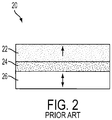
- Fig. 2 is an example of a MTJ stack 20 that includes a pinned layer 22, a tunnel barrier layer 24 and a free magnetic layer 26 where the magnetizations of the free magnetic layer 26 and pinned layer 22 are perpendicular to the plane.
- the layers 22 and 26 have perpendicular magnetic anisotropy (PMA).
- PMA perpendicular magnetic anisotropy
- Some problems associated with the MTJ stack 20 include that there is a minimal number of magnetic materials with perpendicular anisotropy, and these materials have fundamental problems for use in spin-torque MRAM devices. For example, some materials have low magnetoresistance (MR) with a tunnel barrier layer of the MTJ stack and others have to be grown at high temperatures e.g., 500C.
- MR magnetoresistance
- EP 1 693 854 A2 discloses an MRAM with an MTJ and a free layer consisting of repeated stacks of Ta-based seed layers and ferromagnetic layers.
- the spin-torque based MRAM includes a multi-layer MTJ stack that includes a plurality of seed layers each comprising tantalum and a plurality of free magnetic layers comprising at least iron wherein each free magnetic layer of the plurality of free magnetic layers is grown on top of each seed layer of the plurality of seed layers in a stacked manner and each free magnetic layer of the plurality of free magnetic layers is perpendicularly magnetized.
- the magnetic layer may include a seed layer 102 comprises at least tantalum.
- the seed layer 102 may comprise tantalum and magnesium (Mg) wherein the Mg is less than 50% of the composition.
- the magnetic layer further includes a free magnetic layer 104 comprising at least iron (Fe).
- the free magnetic layer 104 is grown on top of the seed layer 102 and the free magnetic layer 104 is perpendicularly magnetized.
- the magnetic layers shown in Fig. 3 may be included in an MTJ stack as depicted in Fig. 8 , for example.
- the seed layer 102 comprises at least 80% tantalum and the free magnetic layer 104 comprises at least 10% iron. Further, the seed layer 102 is of a predetermined thickness ranging from approximately 0.5 nanometers (nm) to approximately 3 nanometers (nm).
- the free magnetic layer 104 may further include at least one of cobalt (Co) and boron (B). Therefore, the free magnetic layer may include CoFeB, for example.
- the CoFeB may be of a variety of compositions.
- the CoFeB composition may include 60% of Co, 20% of Fe and 20% of B.
- Co is less than approximately 90% of the composition of the free magnetic layer 104.
- the composition range of the Fe is between 10% and 100%; and the B is less than approximately 40% of the composition of the free magnetic layer 104.
- the present invention is not limited to the use of CoFeB; other suitable elements may be utilized.
- a predetermined thickness of the free magnetic layer 104 ranges from approximately 0.5 nanometers (nm) to approximately 1.5 nanometers (nm).
- the present invention discloses examples of optimal MTJ stack material choices that provide switching characteristics required for integrated memory applications of a spin-torque switched MTJ.
- the free magnetic layer 104 has a high magnetoresistance (MR).
- the free magnetic layer 104 is in a body-centered cubic (BCC) structure.
- the free magnetic layer 104 is not in the L10 crystal structure (i.e., phase).
- a tunnel barrier layer is formed on top of the free magnetic layer 104 and will now be described with reference to Fig. 4 .
- a tunnel barrier layer 106 is formed on the free magnetic layer 104.
- the tunnel barrier layer 106 is formed of magnesium oxide (MgO) for example.
- MgO magnesium oxide
- the tunnel barrier layer 106 adds anisotropy to an MTJ stack.
- a fixed pinned layer 107 may be grown on top of the tunnel barrier layer 106.
- an interface layer may be grown between the seed layer 102 and the free magnetic layer 104 as shown in Fig. 5 .
- an interface layer 108 comprising a thin layer of Fe is provided.
- the interface layer 108 is formed of a predetermined thickness of less than 0.5 nanometers (nm).
- the seed layer 102 may include approximately 2 nanometers (nm) of tantalum; the interface layer 108 may include approximately 0.3 nanometers (nm) of iron; and the free magnetic layer 104 may include approximately 0.7 nanometers (nm) of CoFeB.
- the interface layer 108 may be a first interface layer.
- An additional interface layer e.g., a second interface layer
- a second interface layer 110 formed of a thin layer of Fe may also be provided to add to the anisotropy of the free layer-tunnel barrier layer interface.
- the second interface layer 110 may be of a predetermined thickness less than or equal to approximately 0.5 nanometers (nm).
- the MTJ stack 100 may include a seed layer 102 of approximately 2 nanometers (nm) of Ta; a first interface layer of approximately 0.3 nanometers (nm) of Fe; a free magnetic layer of approximately 0.7 nanometers of CoFeB; an MgO tunnel barrier layer and a second interface layer 110 of approximately 0.5 nanometers (nm) of Fe.
- a fixed pinned layer such as layer 107 shown in Fig. 4 , may be grown on top of second interface layer 110.
- the pinned magnetic layer may be formed of Co
- the pinned magnetic layer may be formed of at least one of Pt or palladium (Pd), and at least one of CoFe or cobalt (Co).
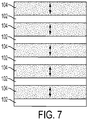
- a multilayer MTJ stack is implemented within embodiments of the present invention for a thicker perpendicular magnetic layer, as discussed below with reference to Fig. 7 .
- a plurality of seed layers 102 each comprising tantalum, for example, is provided.
- a plurality of free magnetic layers 104 is also provided.
- Each free magnetic layer 104 of the plurality of free magnetic layers 104 is grown on top of each seed layer 102 of the plurality of seed layers 102 in a stacked manner.
- Each free magnetic layer 104 of the plurality of free magnetic layers 104 is perpendicularly magnetized.
- each seed layer 102 of the plurality of seed layers 102 is of a predetermined thickness ranging from approximately 0.2 nanometers (nm) to approximately 2 nanometers (nm).
- Each free magnetic layers 104 of the plurality of free magnetic layers 104 includes at least iron.
- the layers 104 may further include at least one of cobalt and boron, for example, layers 104 may include CoFeB.
- the multi-layer stack may include more than two free magnetic layers 104 as shown.
- the seed layers 102 may include tantalum magnesium and the combination may be formed of approximately 2.0 nanometers (nm) of TaMg
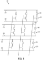
- Fig. 8 is a diagram illustrating a spin-torque based magnetic random access memory (MRAM) device having a plurality of MTJ stacks that can be implemented within embodiments of the present invention.
- the spin-torque based MRAM device 200 includes a plurality of MTJ stacks 205.
- the MTJ stacks 205 comprise the MTJ stack materials as shown in Figs. 3 through 7 .
- Each MTJ stack 205 is connected in series to a transistor 210.
- Each MTJ stack 205 and the transistor 210 are connected together between a bit line 215 and a bit line complement 220. Further, each transistor 210 is connected at a gate thereof to a word line 225.
- the spin-polarized electrons exert a torque on a free magnetic layer of the MTJ stack 205, which can switch the polarity of the free magnetic layer.
- a current is used to detect the resistance/logic state of the MTJ stack 205.
- Each respective transistor 210 is switched on for both read and write operations to allow current to flow through the respective MTJ stack 205, so that the logic state can be read or written.
- Fig. 9 is a graph illustrating the magnetic moment per unit area of the free magnetic layer and the anisotropy field (Hk) of the free magnetic layer.
- the anisotropy field Hk is the in-plane field required to force the moment into the plain.
- the solid lines 300 indicate constant activation energy, proportional to the product of moment and anisotropy.
- the thickness of the free magnetic layer 102 may vary and directly affect the magnetic moment. For example, a plurality of shapes 305 through 325, each represent MTJ stacks having free magnetic layers of different thicknesses.
- the shape 305 represents an MTJ stack having a composition of 20 Ta
- the shape 310 represents an MTJ stack having a composition of 20 Ta
- the shape 315 represents an MTJ stack having a composition of 20 Ta
- the shape 320 represents an MTJ stack having a composition of 20 Ta
- the shape 325 represents an MTJ stack having a composition of 20 Ta
- the 3Fe layer above the MgO tunnel barrier layer 106 is a non-magentic layer and is used to obtain an accurate PMA on the free magnetic layer 104 (which depends on the oxidation condition of the MgO tunnel barrier layer 106).
- a MTJ stack may be provided having a Co
- the MTJ stack materials of embodiments of the present invention have perpendicular magnetic anisotropy (PMA) and provide high magnetoresistance (MR) with a tunnel barrier layer of the MTJ stack and can be grown at room temperature.
- the MTJ stack materials include a seed layer including tantalum and a free magnetic layer comprising at least iron.
Landscapes
- Engineering & Computer Science (AREA)
- Chemical & Material Sciences (AREA)
- Crystallography & Structural Chemistry (AREA)
- Power Engineering (AREA)
- Nanotechnology (AREA)
- Computer Hardware Design (AREA)
- Manufacturing & Machinery (AREA)
- Hall/Mr Elements (AREA)
- Mram Or Spin Memory Techniques (AREA)
Description
- The present invention relates to magnetic random access memory, and more specifically, to materials optimized for spin-torque memory having a seed layer and free magnetic layer for perpendicular anisotropy.
- A spin torque magnetic random access memory (MRAM) device uses a two terminal spin-torque based memory element including a pinned layer, a tunnel barrier layer and a free layer in a magnetic tunnel junction (MTJ) stack as shown in
Figs. 1 and2 . For example, inFig. 1 , aMTJ stack 10 includes a pinnedlayer 12, atunnel barrier layer 14 and a freemagnetic layer 16. The magnetization of thepinned layer 12 is fixed in a direction (e.g., in a horizontal direction to the right as shown inFig. 1 or in a vertically direction pointing up as shown inFig. 2 ). The current passing up through theMTJ stack 10 makes the freemagnetic layer 16 parallel to pinnedlayer 12, while a current passing down through theMTJ stack 10 makes the freemagnetic layer 16 anti-parallel to thepinned layer 12. A smaller current (of either polarity) is used to read the resistance of the device, which depends on the relative orientations of thefree layer 16 and pinnedlayer 12. As shown inFig. 1 , the freemagnetic layer 16 and pinnedlayer 12 have their magnetizations lie in the plane which may lead to high switching currents. -
Fig. 2 is an example of aMTJ stack 20 that includes a pinnedlayer 22, atunnel barrier layer 24 and a freemagnetic layer 26 where the magnetizations of the freemagnetic layer 26 and pinnedlayer 22 are perpendicular to the plane. Thelayers MTJ stack 20 include that there is a minimal number of magnetic materials with perpendicular anisotropy, and these materials have fundamental problems for use in spin-torque MRAM devices. For example, some materials have low magnetoresistance (MR) with a tunnel barrier layer of the MTJ stack and others have to be grown at high temperatures e.g., 500C.EP 1 693 854 A2 discloses an MRAM with an MTJ and a free layer consisting of repeated stacks of Ta-based seed layers and ferromagnetic layers. - The present invention is defined in the appended claim 1.
- A spin-torque MRAM device is provided. The spin-torque based MRAM includes a multi-layer MTJ stack that includes a plurality of seed layers each comprising tantalum and a plurality of free magnetic layers comprising at least iron wherein each free magnetic layer of the plurality of free magnetic layers is grown on top of each seed layer of the plurality of seed layers in a stacked manner and each free magnetic layer of the plurality of free magnetic layers is perpendicularly magnetized.
- Additional features and advantages are realized through the techniques of the present invention. For a better understanding of the invention with the advantages and the features, refer to the description and to the drawings.
- The subject matter which is regarded as the invention is particularly pointed out and distinctly claimed in the claims at the conclusion of the specification. The forgoing and other features, and advantages of the invention are apparent from the following detailed description taken in conjunction with the accompanying drawings in which:
-
Figs. 1 and2 are diagrams illustrating conventional magnetic tunnel junction (MTJ) stacks. -
Fig. 3 is a diagram illustrating a seed layer and a free magnetic layer of an MTJ stack that can be implemented within embodiments of the present invention. -
Fig. 4 is a diagram illustrating the MTJ stack shown inFig. 3 including a tunnel barrier layer that can be implemented within alternative embodiments of the present invention. -
Fig. 5 is a diagram illustrating a first interface material layer of iron formed between the seed layer and the free magnetic layer of a MTJ stack that can be implemented within embodiments of the present invention. -
Fig. 6 is a diagram illustrating a second interface layer of iron formed on the tunnel barrier layer that can be implemented within embodiments of the present invention. -
Fig. 7 is a diagram illustrating a multilayer MTJ stack that can be implemented within embodiments of the present invention. -
Fig. 8 is a diagram illustrating a magnetic random access memory (MRAM) device including MTJ stacks that can be implemented within embodiments of the present invention. -
Fig. 9 is a graph illustrating the magnetic moment per unit area of the free magnetic layer and the anisotropy field (Hk) of the free magnetic layer. - With reference now to
Fig. 3 , a magnetic layer is provided. As shown inFig. 3 , the magnetic layer may include aseed layer 102 comprises at least tantalum. Alternatively, theseed layer 102 may comprise tantalum and magnesium (Mg) wherein the Mg is less than 50% of the composition. The magnetic layer further includes a freemagnetic layer 104 comprising at least iron (Fe). The freemagnetic layer 104 is grown on top of theseed layer 102 and the freemagnetic layer 104 is perpendicularly magnetized. According to an embodiment of the present invention the magnetic layers shown inFig. 3 , may be included in an MTJ stack as depicted inFig. 8 , for example. According to an embodiment of the present invention, theseed layer 102 comprises at least 80% tantalum and the freemagnetic layer 104 comprises at least 10% iron. Further, theseed layer 102 is of a predetermined thickness ranging from approximately 0.5 nanometers (nm) to approximately 3 nanometers (nm). - According to an embodiment of the present invention, the free
magnetic layer 104 may further include at least one of cobalt (Co) and boron (B). Therefore, the free magnetic layer may include CoFeB, for example. The CoFeB may be of a variety of compositions. For example, the CoFeB composition may include 60% of Co, 20% of Fe and 20% of B. According to an embodiment of the present invention, Co is less than approximately 90% of the composition of the freemagnetic layer 104. The composition range of the Fe is between 10% and 100%; and the B is less than approximately 40% of the composition of the freemagnetic layer 104. The present invention is not limited to the use of CoFeB; other suitable elements may be utilized. According to an embodiment of the present invention, a predetermined thickness of the freemagnetic layer 104 ranges from approximately 0.5 nanometers (nm) to approximately 1.5 nanometers (nm). - The present invention discloses examples of optimal MTJ stack material choices that provide switching characteristics required for integrated memory applications of a spin-torque switched MTJ. For example, according to one embodiment of the present invention, the free
magnetic layer 104 has a high magnetoresistance (MR). According to another embodiment of the present invention, the freemagnetic layer 104 is in a body-centered cubic (BCC) structure. According to another embodiment of the present invention, the freemagnetic layer 104 is not in the L10 crystal structure (i.e., phase). - According to an embodiment of the present invention, a tunnel barrier layer is formed on top of the free
magnetic layer 104 and will now be described with reference toFig. 4 . As shown inFig. 4 , atunnel barrier layer 106 is formed on the freemagnetic layer 104. Thetunnel barrier layer 106 is formed of magnesium oxide (MgO) for example. Thetunnel barrier layer 106 adds anisotropy to an MTJ stack. According to another embodiment of the present invention, a fixed pinnedlayer 107 may be grown on top of thetunnel barrier layer 106. - Further, according to the current embodiment of the present invention, an interface layer may be grown between the
seed layer 102 and the freemagnetic layer 104 as shown inFig. 5 . InFig. 5 , aninterface layer 108 comprising a thin layer of Fe is provided. According to an embodiment of the present invention, theinterface layer 108 is formed of a predetermined thickness of less than 0.5 nanometers (nm). According to an embodiment of the present invention, theseed layer 102 may include approximately 2 nanometers (nm) of tantalum; theinterface layer 108 may include approximately 0.3 nanometers (nm) of iron; and the freemagnetic layer 104 may include approximately 0.7 nanometers (nm) of CoFeB. According to an embodiment of the present invention, theinterface layer 108 may be a first interface layer. An additional interface layer (e.g., a second interface layer) may be included in an MTJ stack as discussed below with reference toFig. 6 . - As shown in
Fig. 6 , according to another embodiment of the present invention, asecond interface layer 110 formed of a thin layer of Fe may also be provided to add to the anisotropy of the free layer-tunnel barrier layer interface. Thesecond interface layer 110 may be of a predetermined thickness less than or equal to approximately 0.5 nanometers (nm). According to an embodiment of the present invention, theMTJ stack 100 may include aseed layer 102 of approximately 2 nanometers (nm) of Ta; a first interface layer of approximately 0.3 nanometers (nm) of Fe; a free magnetic layer of approximately 0.7 nanometers of CoFeB; an MgO tunnel barrier layer and asecond interface layer 110 of approximately 0.5 nanometers (nm) of Fe. A fixed pinned layer such aslayer 107 shown inFig. 4 , may be grown on top ofsecond interface layer 110. The pinned magnetic layer may be formed of Co|Pd or Co|Pt multilayers, for example. The pinned magnetic layer may be formed of at least one of Pt or palladium (Pd), and at least one of CoFe or cobalt (Co). - According to the present invention, a multilayer MTJ stack is implemented within embodiments of the present invention for a thicker perpendicular magnetic layer, as discussed below with reference to
Fig. 7 . InFig. 7 , a plurality ofseed layers 102 each comprising tantalum, for example, is provided. Further, a plurality of freemagnetic layers 104 is also provided. Each freemagnetic layer 104 of the plurality of freemagnetic layers 104 is grown on top of eachseed layer 102 of the plurality ofseed layers 102 in a stacked manner. Each freemagnetic layer 104 of the plurality of freemagnetic layers 104 is perpendicularly magnetized. According to an embodiment of the present invention, eachseed layer 102 of the plurality of seed layers 102 is of a predetermined thickness ranging from approximately 0.2 nanometers (nm) to approximately 2 nanometers (nm). Each freemagnetic layers 104 of the plurality of freemagnetic layers 104 includes at least iron. Thelayers 104 may further include at least one of cobalt and boron, for example, layers 104 may include CoFeB. The multi-layer stack may include more than two freemagnetic layers 104 as shown. The seed layers 102 may include tantalum magnesium and the combination may be formed of approximately 2.0 nanometers (nm) of TaMg| {0.6 nm Fe| 0.3nm of TaMg} x N| 0.6 nm Fe, where N is a positive integer. -
Fig. 8 is a diagram illustrating a spin-torque based magnetic random access memory (MRAM) device having a plurality of MTJ stacks that can be implemented within embodiments of the present invention. As shown inFig. 8 , the spin-torque basedMRAM device 200 includes a plurality of MTJ stacks 205. According to an embodiment of the present invention, the MTJ stacks 205 comprise the MTJ stack materials as shown inFigs. 3 through 7 . EachMTJ stack 205 is connected in series to atransistor 210. EachMTJ stack 205 and thetransistor 210 are connected together between abit line 215 and abit line complement 220. Further, eachtransistor 210 is connected at a gate thereof to aword line 225. During a write operation, the spin-polarized electrons exert a torque on a free magnetic layer of theMTJ stack 205, which can switch the polarity of the free magnetic layer. During a read operation, a current is used to detect the resistance/logic state of theMTJ stack 205. Eachrespective transistor 210 is switched on for both read and write operations to allow current to flow through therespective MTJ stack 205, so that the logic state can be read or written. -
Fig. 9 is a graph illustrating the magnetic moment per unit area of the free magnetic layer and the anisotropy field (Hk) of the free magnetic layer. The units used are Oersted
solid lines 300 indicate constant activation energy, proportional to the product of moment and anisotropy. The thickness of the freemagnetic layer 102 may vary and directly affect the magnetic moment. For example, a plurality ofshapes 305 through 325, each represent MTJ stacks having free magnetic layers of different thicknesses. For example, theshape 305 represents an MTJ stack having a composition of 20 Ta|X CoFeB|10 MgO|3Fe|50 TaN where X is equal to 8, 9 or 10. Theshape 310 represents an MTJ stack having a composition of 20 Ta|2Fe| X CoFeB|10 MgO|3Fe|50 TaN where X is equal to 7, 8 or 9. Theshape 315 represents an MTJ stack having a composition of 20 Ta|3Fe|XCoFeB|10MgO|3Fe|50 TaN where X is equal to 6, 7 or 8. The shape 320 represents an MTJ stack having a composition of 20 Ta|3Fe|X CoFeB|3Ta|3Fe|6CoFeB|10MgO|3Fe|50 TaN where X is equal to 6 or 8. Theshape 325 represents an MTJ stack having a composition of 20 Ta|3Fe|3CoFeB|3Fe|3Ta|3Fe| 6CoFeB|10MgO|3Fe|50 TaN. According to an embodiment of the present invention, as the thickness of the freemagnetic layer 104 increases the moment increases, as shown inFig. 9 . In these examples of the present invention, the 3Fe layer above the MgOtunnel barrier layer 106 is a non-magentic layer and is used to obtain an accurate PMA on the free magnetic layer 104 (which depends on the oxidation condition of the MgO tunnel barrier layer 106). According to another embodiment of the present invention, a MTJ stack may be provided having a Co|Pd or Co|Pt multilayer above the 3Fe layer. - The MTJ stack materials of embodiments of the present invention have perpendicular magnetic anisotropy (PMA) and provide high magnetoresistance (MR) with a tunnel barrier layer of the MTJ stack and can be grown at room temperature. For example, the MTJ stack materials include a seed layer including tantalum and a free magnetic layer comprising at least iron.
Claims (11)
- A spin-torque magnetic random access memory (MRAM) (200) device comprising:
a multi-layer magnetic tunnel junction stack (MTJ) comprising:a plurality of seed layers (102) each comprising at least tantalum; anda plurality of free magnetic layers (104) comprising at least iron wherein each free magnetic layer of the plurality of free magnetic layers is grown on top of each seed layer of the plurality of seed layers in a stacked manner, and characterized in that each free magnetic layer of the plurality of free magnetic layers is perpendicularly magnetized. - The spin-torque MRAM device (200) of claim 1, wherein a predetermined thickness of each seed layer (102) of the plurality of seed layers ranges from approximately 0.2 to approximately 2 nanometers (nm).
- The spin-torque MRAM device of claim 1 or 2, wherein each free magnetic layer (104) of the plurality of free magnetic layers further comprises at least one of cobalt and boron.
- The spin-torque MRAM device of any preceding claim wherein each of the plurality of free magnetic layers (104) is of a predetermined thickness ranging from approximately 0.2 nm to 1.5 nm.
- A spin-torque MRAM device according to any preceding claim, further comprising:
a tunnel barrier layer (106) formed of magnesium oxide (MgO). - A spin-torque MRAM device according to claim 5, further comprising:
a fixed pinned layer (107) grown on top of the tunnel barrier layer. - A spin-torque MRAM device according to any preceding claim, wherein the seed layers (102) comprise at least 80% tantalum.
- A spin-torque MRAM device according to any preceding claim, wherein the free magnetic layers (104) comprise at least 10% iron.
- A spin-torque MRAM device according to any preceding claim, wherein each seed layer (102) comprises tantalum and magnesium, wherein the magnesium ranges from approximately 0% to approximately 50%.
- A spin-torque MRAM device according to claim 3, wherein the cobalt is less than 90% of a composition of the free magnetic layer (104).
- A spin-torque MRAM device according to claim 10, wherein the boron is less than 40% of a composition of each free magnetic layer (104).
Applications Claiming Priority (2)
| Application Number | Priority Date | Filing Date | Title |
|---|---|---|---|
| US12/815,923 US8324697B2 (en) | 2010-06-15 | 2010-06-15 | Seed layer and free magnetic layer for perpendicular anisotropy in a spin-torque magnetic random access memory |
| PCT/US2011/036910 WO2011159422A1 (en) | 2010-06-15 | 2011-05-18 | Seed layer and free magnetic layer for perpendicular anisotropy in a spin-torque magnetic random access memory |
Publications (3)
| Publication Number | Publication Date |
|---|---|
| EP2583278A1 EP2583278A1 (en) | 2013-04-24 |
| EP2583278A4 EP2583278A4 (en) | 2017-03-22 |
| EP2583278B1 true EP2583278B1 (en) | 2018-09-26 |
Family
ID=45095550
Family Applications (1)
| Application Number | Title | Priority Date | Filing Date |
|---|---|---|---|
| EP11796130.0A Active EP2583278B1 (en) | 2010-06-15 | 2011-05-18 | Seed layer and free magnetic layer for perpendicular anisotropy in a spin-torque magnetic random access memory |
Country Status (7)
| Country | Link |
|---|---|
| US (2) | US8324697B2 (en) |
| EP (1) | EP2583278B1 (en) |
| JP (1) | JP5868394B2 (en) |
| KR (1) | KR101409016B1 (en) |
| CN (1) | CN102893332B (en) |
| TW (1) | TWI497783B (en) |
| WO (1) | WO2011159422A1 (en) |
Families Citing this family (38)
| Publication number | Priority date | Publication date | Assignee | Title |
|---|---|---|---|---|
| JP5742142B2 (en) * | 2010-09-08 | 2015-07-01 | ソニー株式会社 | Memory element and memory device |
| US8508006B2 (en) * | 2011-05-10 | 2013-08-13 | Magic Technologies, Inc. | Co/Ni multilayers with improved out-of-plane anisotropy for magnetic device applications |
| KR101849677B1 (en) * | 2011-05-19 | 2018-04-19 | 삼성전자주식회사 | Magnetic Tunnel Junction Element |
| US8946834B2 (en) * | 2012-03-01 | 2015-02-03 | Headway Technologies, Inc. | High thermal stability free layer with high out-of-plane anisotropy for magnetic device applications |
| US9007818B2 (en) | 2012-03-22 | 2015-04-14 | Micron Technology, Inc. | Memory cells, semiconductor device structures, systems including such cells, and methods of fabrication |
| US8923038B2 (en) | 2012-06-19 | 2014-12-30 | Micron Technology, Inc. | Memory cells, semiconductor device structures, memory systems, and methods of fabrication |
| US9054030B2 (en) | 2012-06-19 | 2015-06-09 | Micron Technology, Inc. | Memory cells, semiconductor device structures, memory systems, and methods of fabrication |
| JP2014033076A (en) * | 2012-08-03 | 2014-02-20 | Toshiba Corp | Magnetoresistance effect element |
| US9490054B2 (en) | 2012-10-11 | 2016-11-08 | Headway Technologies, Inc. | Seed layer for multilayer magnetic materials |
| US9379315B2 (en) | 2013-03-12 | 2016-06-28 | Micron Technology, Inc. | Memory cells, methods of fabrication, semiconductor device structures, and memory systems |
| US9059399B2 (en) | 2013-06-06 | 2015-06-16 | International Business Machines Corporation | Magnetic materials with enhanced perpendicular anisotropy energy density for STT-RAM |
| US9059389B2 (en) | 2013-06-06 | 2015-06-16 | International Business Machines Corporation | Free layers with iron interfacial layer and oxide cap for high perpendicular anisotropy energy density |
| US9087543B2 (en) | 2013-06-06 | 2015-07-21 | International Business Machines Corporation | Spin torque MRAM having perpendicular magnetization with oxide interface |
| US9368714B2 (en) | 2013-07-01 | 2016-06-14 | Micron Technology, Inc. | Memory cells, methods of operation and fabrication, semiconductor device structures, and memory systems |
| US9466787B2 (en) | 2013-07-23 | 2016-10-11 | Micron Technology, Inc. | Memory cells, methods of fabrication, semiconductor device structures, memory systems, and electronic systems |
| US9461242B2 (en) | 2013-09-13 | 2016-10-04 | Micron Technology, Inc. | Magnetic memory cells, methods of fabrication, semiconductor devices, memory systems, and electronic systems |
| US9608197B2 (en) | 2013-09-18 | 2017-03-28 | Micron Technology, Inc. | Memory cells, methods of fabrication, and semiconductor devices |
| US10454024B2 (en) | 2014-02-28 | 2019-10-22 | Micron Technology, Inc. | Memory cells, methods of fabrication, and memory devices |
| EP3123537A4 (en) * | 2014-03-25 | 2018-02-14 | Intel Corporation | Magnetic domain wall logic devices and interconnect |
| US9281466B2 (en) | 2014-04-09 | 2016-03-08 | Micron Technology, Inc. | Memory cells, semiconductor structures, semiconductor devices, and methods of fabrication |
| US9269888B2 (en) | 2014-04-18 | 2016-02-23 | Micron Technology, Inc. | Memory cells, methods of fabrication, and semiconductor devices |
| US20150333254A1 (en) | 2014-05-15 | 2015-11-19 | Headway Technologies, Inc. | Reduction of Barrier Resistance X Area (RA) Product and Protection of Perpendicular Magnetic Anisotropy (PMA) for Magnetic Device Applications |
| WO2016048376A1 (en) * | 2014-09-26 | 2016-03-31 | Intel Corporation | Amorphous seed layer for improved stability in perpendicular sttm stack |
| US9349945B2 (en) | 2014-10-16 | 2016-05-24 | Micron Technology, Inc. | Memory cells, semiconductor devices, and methods of fabrication |
| US9768377B2 (en) | 2014-12-02 | 2017-09-19 | Micron Technology, Inc. | Magnetic cell structures, and methods of fabrication |
| US10439131B2 (en) | 2015-01-15 | 2019-10-08 | Micron Technology, Inc. | Methods of forming semiconductor devices including tunnel barrier materials |
| KR102465539B1 (en) | 2015-09-18 | 2022-11-11 | 삼성전자주식회사 | Semiconductor device having a magnetic tunnel junction assembly, and Mehtod for fabricating the same |
| US10115892B2 (en) | 2015-11-23 | 2018-10-30 | Headway Technologies, Inc. | Multilayer structure for reducing film roughness in magnetic devices |
| US9780299B2 (en) | 2015-11-23 | 2017-10-03 | Headway Technologies, Inc. | Multilayer structure for reducing film roughness in magnetic devices |
| US10361361B2 (en) * | 2016-04-08 | 2019-07-23 | International Business Machines Corporation | Thin reference layer for STT MRAM |
| US10304603B2 (en) * | 2016-06-29 | 2019-05-28 | International Business Machines Corporation | Stress control in magnetic inductor stacks |
| US10811177B2 (en) * | 2016-06-30 | 2020-10-20 | International Business Machines Corporation | Stress control in magnetic inductor stacks |
| US10283249B2 (en) | 2016-09-30 | 2019-05-07 | International Business Machines Corporation | Method for fabricating a magnetic material stack |
| JP2019057636A (en) | 2017-09-21 | 2019-04-11 | 東芝メモリ株式会社 | Magnetic memory device |
| US10833255B2 (en) * | 2017-09-21 | 2020-11-10 | Hitachi High-Tech Corporation | Method for manufacturing magnetic tunnel junction element, and inductively coupled plasma processing apparatus |
| US10468171B1 (en) | 2018-06-27 | 2019-11-05 | Globalfoundries Singapore Pte. Ltd. | Integrated circuits with magnetic tunnel junctions and methods of producing the same |
| US10648069B2 (en) | 2018-10-16 | 2020-05-12 | Taiwan Semiconductor Manufacturing Company, Ltd. | Monolayer-by-monolayer growth of MgO layers using Mg sublimation and oxidation |
| US11469371B2 (en) * | 2019-08-29 | 2022-10-11 | Taiwan Semiconductor Manufacturing Company, Ltd. | SOT-MRAM cell in high density applications |
Family Cites Families (27)
| Publication number | Priority date | Publication date | Assignee | Title |
|---|---|---|---|---|
| US7105240B2 (en) | 2003-06-03 | 2006-09-12 | Seagate Technology Llc | Perpendicular media with improved corrosion performance |
| JP4253225B2 (en) * | 2003-07-09 | 2009-04-08 | 株式会社東芝 | Magnetoresistive element and magnetic memory |
| US6967863B2 (en) * | 2004-02-25 | 2005-11-22 | Grandis, Inc. | Perpendicular magnetization magnetic element utilizing spin transfer |
| US7313013B2 (en) | 2004-11-18 | 2007-12-25 | International Business Machines Corporation | Spin-current switchable magnetic memory element and method of fabricating the memory element |
| JP5077802B2 (en) * | 2005-02-16 | 2012-11-21 | 日本電気株式会社 | Laminated ferromagnetic structure and MTJ element |
| US7489541B2 (en) | 2005-08-23 | 2009-02-10 | Grandis, Inc. | Spin-transfer switching magnetic elements using ferrimagnets and magnetic memories using the magnetic elements |
| US7973349B2 (en) * | 2005-09-20 | 2011-07-05 | Grandis Inc. | Magnetic device having multilayered free ferromagnetic layer |
| US20070096229A1 (en) | 2005-10-28 | 2007-05-03 | Masatoshi Yoshikawa | Magnetoresistive element and magnetic memory device |
| US7446984B2 (en) * | 2005-12-14 | 2008-11-04 | Hitachi Global Storage Technologies Netherlands B.V. | Magnetic random access memory (MRAM) having increased reference layer anisotropy through ion beam etch of magnetic layers |
| US8084835B2 (en) | 2006-10-20 | 2011-12-27 | Avalanche Technology, Inc. | Non-uniform switching based non-volatile magnetic based memory |
| JP4564933B2 (en) | 2006-03-15 | 2010-10-20 | ヒタチグローバルストレージテクノロジーズネザーランドビーブイ | Perpendicular magnetic recording medium, magnetic characteristic evaluation method thereof, and magnetic recording / reproducing apparatus |
| DE602006013948D1 (en) * | 2006-05-04 | 2010-06-10 | Hitachi Ltd | Magnetic memory device |
| US7535069B2 (en) * | 2006-06-14 | 2009-05-19 | International Business Machines Corporation | Magnetic tunnel junction with enhanced magnetic switching characteristics |
| JP4384183B2 (en) * | 2007-01-26 | 2009-12-16 | 株式会社東芝 | Magnetoresistive element and magnetic memory |
| US20090218645A1 (en) | 2007-02-12 | 2009-09-03 | Yadav Technology Inc. | multi-state spin-torque transfer magnetic random access memory |
| JP2008252018A (en) | 2007-03-30 | 2008-10-16 | Toshiba Corp | Magnetoresistive element and magnetic random access memory using the same |
| CN101689600B (en) * | 2007-06-25 | 2012-12-26 | 日本电气株式会社 | Magnetoresistive element and magnetic random access memory |
| US20090027948A1 (en) | 2007-07-24 | 2009-01-29 | Manfred Ruehrig | Integrated Circuits, Method of Programming a Cell, Thermal Select Magnetoresistive Element, Memory Module |
| JP4738395B2 (en) * | 2007-09-25 | 2011-08-03 | 株式会社東芝 | Magnetoresistive element and magnetic random access memory using the same |
| JP4649457B2 (en) * | 2007-09-26 | 2011-03-09 | 株式会社東芝 | Magnetoresistive element and magnetic memory |
| JP2009116952A (en) | 2007-11-06 | 2009-05-28 | Hitachi Global Storage Technologies Netherlands Bv | Perpendicular magnetic recording medium and magnetic storage device using the same |
| JP4599425B2 (en) | 2008-03-27 | 2010-12-15 | 株式会社東芝 | Magnetoresistive element and magnetic memory |
| JP2010034153A (en) | 2008-07-25 | 2010-02-12 | Toshiba Corp | Magnetic random access memory and method for writing the same |
| JP4772845B2 (en) | 2008-09-29 | 2011-09-14 | 株式会社東芝 | Magnetic random access memory and manufacturing method thereof |
| WO2010080542A1 (en) * | 2008-12-17 | 2010-07-15 | Yadav Technology, Inc. | Spin-transfer torque magnetic random access memory having magnetic tunnel junction with perpendicular magnetic anisotropy |
| US8283741B2 (en) * | 2010-01-08 | 2012-10-09 | International Business Machines Corporation | Optimized free layer for spin torque magnetic random access memory |
| JP5725735B2 (en) * | 2010-06-04 | 2015-05-27 | 株式会社日立製作所 | Magnetoresistive element and magnetic memory |
-
2010
- 2010-06-15 US US12/815,923 patent/US8324697B2/en active Active
-
2011
- 2011-05-18 CN CN201180024160.4A patent/CN102893332B/en active Active
- 2011-05-18 JP JP2013515346A patent/JP5868394B2/en active Active
- 2011-05-18 WO PCT/US2011/036910 patent/WO2011159422A1/en not_active Ceased
- 2011-05-18 KR KR1020127026965A patent/KR101409016B1/en active Active
- 2011-05-18 EP EP11796130.0A patent/EP2583278B1/en active Active
- 2011-06-15 TW TW100120919A patent/TWI497783B/en active
-
2012
- 2012-08-09 US US13/570,375 patent/US8536668B2/en active Active
Non-Patent Citations (1)
| Title |
|---|
| None * |
Also Published As
| Publication number | Publication date |
|---|---|
| KR101409016B1 (en) | 2014-06-18 |
| WO2011159422A1 (en) | 2011-12-22 |
| US8536668B2 (en) | 2013-09-17 |
| CN102893332A (en) | 2013-01-23 |
| JP5868394B2 (en) | 2016-02-24 |
| US20110303995A1 (en) | 2011-12-15 |
| KR20130018773A (en) | 2013-02-25 |
| CN102893332B (en) | 2015-10-07 |
| US8324697B2 (en) | 2012-12-04 |
| TW201212314A (en) | 2012-03-16 |
| TWI497783B (en) | 2015-08-21 |
| US20120299137A1 (en) | 2012-11-29 |
| JP2013528955A (en) | 2013-07-11 |
| EP2583278A1 (en) | 2013-04-24 |
| EP2583278A4 (en) | 2017-03-22 |
Similar Documents
| Publication | Publication Date | Title |
|---|---|---|
| US8536668B2 (en) | Seed layer and free magnetic layer for perpindicular anisotropy in a spin-torque magnetic random access memory | |
| US20130059168A1 (en) | Magnetoresistance Device | |
| US8492859B2 (en) | Magnetic tunnel junction with spacer layer for spin torque switched MRAM | |
| US10003016B2 (en) | Perpendicular magnetic anisotropy BCC multilayers | |
| US8283741B2 (en) | Optimized free layer for spin torque magnetic random access memory | |
| US20120241878A1 (en) | Magnetic tunnel junction with iron dusting layer between free layer and tunnel barrier | |
| US8406040B2 (en) | Spin-torque based memory device using a magnesium oxide tunnel barrier | |
| CN102916126B (en) | Storage Elements and Storage Devices | |
| JP6244617B2 (en) | Storage element, storage device, magnetic head | |
| JP2012533189A (en) | Magnetic stack with reference layer with orthogonal magnetization orientation direction | |
| US20120104522A1 (en) | Magnetic tunnel junction cells having perpendicular anisotropy and enhancement layer | |
| US12283296B2 (en) | Spin-transfer torque magnetoresistive memory device with a free layer stack including multiple spacers and methods of making the same | |
| TWI639155B (en) | Storage component, storage device and magnetic head | |
| CN102610270B (en) | Memory element and storage arrangement | |
| JPWO2012004883A1 (en) | Magnetoresistive element and random access memory using the same | |
| EP2887410A1 (en) | Magnetic multilayer stack | |
| KR101635139B1 (en) | Magnetic memory devices | |
| WO2023111769A1 (en) | Paramagnetic hexagonal metal phase coupling spacer | |
| JP2017212464A (en) | Storage element, storage device, magnetic head |
Legal Events
| Date | Code | Title | Description |
|---|---|---|---|
| PUAI | Public reference made under article 153(3) epc to a published international application that has entered the european phase |
Free format text: ORIGINAL CODE: 0009012 |
|
| 17P | Request for examination filed |
Effective date: 20130103 |
|
| AK | Designated contracting states |
Kind code of ref document: A1 Designated state(s): AL AT BE BG CH CY CZ DE DK EE ES FI FR GB GR HR HU IE IS IT LI LT LU LV MC MK MT NL NO PL PT RO RS SE SI SK SM TR |
|
| DAX | Request for extension of the european patent (deleted) | ||
| RA4 | Supplementary search report drawn up and despatched (corrected) |
Effective date: 20170217 |
|
| RIC1 | Information provided on ipc code assigned before grant |
Ipc: H01F 10/30 20060101ALI20170213BHEP Ipc: H01L 43/10 20060101ALI20170213BHEP Ipc: B82Y 25/00 20110101ALN20170213BHEP Ipc: H01F 10/32 20060101ALI20170213BHEP Ipc: G11C 11/16 20060101AFI20170213BHEP Ipc: H01L 43/08 20060101ALI20170213BHEP |
|
| REG | Reference to a national code |
Ref country code: DE Ref legal event code: R079 Ref document number: 602011052403 Country of ref document: DE Free format text: PREVIOUS MAIN CLASS: G11B0005330000 Ipc: G11C0011160000 |
|
| RIC1 | Information provided on ipc code assigned before grant |
Ipc: H01F 10/30 20060101ALI20180424BHEP Ipc: G11C 11/16 20060101AFI20180424BHEP Ipc: B82Y 25/00 20110101ALN20180424BHEP Ipc: H01L 43/08 20060101ALI20180424BHEP Ipc: H01F 10/32 20060101ALI20180424BHEP Ipc: H01L 43/10 20060101ALI20180424BHEP |
|
| INTG | Intention to grant announced |
Effective date: 20180611 |
|
| GRAP | Despatch of communication of intention to grant a patent |
Free format text: ORIGINAL CODE: EPIDOSNIGR1 |
|
| STAA | Information on the status of an ep patent application or granted ep patent |
Free format text: STATUS: GRANT OF PATENT IS INTENDED |
|
| GRAS | Grant fee paid |
Free format text: ORIGINAL CODE: EPIDOSNIGR3 |
|
| GRAA | (expected) grant |
Free format text: ORIGINAL CODE: 0009210 |
|
| STAA | Information on the status of an ep patent application or granted ep patent |
Free format text: STATUS: THE PATENT HAS BEEN GRANTED |
|
| AK | Designated contracting states |
Kind code of ref document: B1 Designated state(s): AL AT BE BG CH CY CZ DE DK EE ES FI FR GB GR HR HU IE IS IT LI LT LU LV MC MK MT NL NO PL PT RO RS SE SI SK SM TR |
|
| REG | Reference to a national code |
Ref country code: GB Ref legal event code: FG4D |
|
| REG | Reference to a national code |
Ref country code: CH Ref legal event code: EP |
|
| REG | Reference to a national code |
Ref country code: DE Ref legal event code: R084 Ref document number: 602011052403 Country of ref document: DE |
|
| REG | Reference to a national code |
Ref country code: AT Ref legal event code: REF Ref document number: 1046965 Country of ref document: AT Kind code of ref document: T Effective date: 20181015 Ref country code: CH Ref legal event code: NV Representative=s name: IBM RESEARCH GMBH ZURICH RESEARCH LABORATORY I, CH |
|
| REG | Reference to a national code |
Ref country code: IE Ref legal event code: FG4D |
|
| REG | Reference to a national code |
Ref country code: DE Ref legal event code: R096 Ref document number: 602011052403 Country of ref document: DE |
|
| REG | Reference to a national code |
Ref country code: GB Ref legal event code: 746 Effective date: 20181008 |
|
| REG | Reference to a national code |
Ref country code: NL Ref legal event code: MP Effective date: 20180926 |
|
| PG25 | Lapsed in a contracting state [announced via postgrant information from national office to epo] |
Ref country code: SE Free format text: LAPSE BECAUSE OF FAILURE TO SUBMIT A TRANSLATION OF THE DESCRIPTION OR TO PAY THE FEE WITHIN THE PRESCRIBED TIME-LIMIT Effective date: 20180926 Ref country code: FI Free format text: LAPSE BECAUSE OF FAILURE TO SUBMIT A TRANSLATION OF THE DESCRIPTION OR TO PAY THE FEE WITHIN THE PRESCRIBED TIME-LIMIT Effective date: 20180926 Ref country code: LT Free format text: LAPSE BECAUSE OF FAILURE TO SUBMIT A TRANSLATION OF THE DESCRIPTION OR TO PAY THE FEE WITHIN THE PRESCRIBED TIME-LIMIT Effective date: 20180926 Ref country code: NO Free format text: LAPSE BECAUSE OF FAILURE TO SUBMIT A TRANSLATION OF THE DESCRIPTION OR TO PAY THE FEE WITHIN THE PRESCRIBED TIME-LIMIT Effective date: 20181226 Ref country code: RS Free format text: LAPSE BECAUSE OF FAILURE TO SUBMIT A TRANSLATION OF THE DESCRIPTION OR TO PAY THE FEE WITHIN THE PRESCRIBED TIME-LIMIT Effective date: 20180926 Ref country code: GR Free format text: LAPSE BECAUSE OF FAILURE TO SUBMIT A TRANSLATION OF THE DESCRIPTION OR TO PAY THE FEE WITHIN THE PRESCRIBED TIME-LIMIT Effective date: 20181227 Ref country code: BG Free format text: LAPSE BECAUSE OF FAILURE TO SUBMIT A TRANSLATION OF THE DESCRIPTION OR TO PAY THE FEE WITHIN THE PRESCRIBED TIME-LIMIT Effective date: 20181226 |
|
| REG | Reference to a national code |
Ref country code: LT Ref legal event code: MG4D |
|
| PG25 | Lapsed in a contracting state [announced via postgrant information from national office to epo] |
Ref country code: HR Free format text: LAPSE BECAUSE OF FAILURE TO SUBMIT A TRANSLATION OF THE DESCRIPTION OR TO PAY THE FEE WITHIN THE PRESCRIBED TIME-LIMIT Effective date: 20180926 Ref country code: LV Free format text: LAPSE BECAUSE OF FAILURE TO SUBMIT A TRANSLATION OF THE DESCRIPTION OR TO PAY THE FEE WITHIN THE PRESCRIBED TIME-LIMIT Effective date: 20180926 Ref country code: AL Free format text: LAPSE BECAUSE OF FAILURE TO SUBMIT A TRANSLATION OF THE DESCRIPTION OR TO PAY THE FEE WITHIN THE PRESCRIBED TIME-LIMIT Effective date: 20180926 |
|
| REG | Reference to a national code |
Ref country code: AT Ref legal event code: MK05 Ref document number: 1046965 Country of ref document: AT Kind code of ref document: T Effective date: 20180926 |
|
| PG25 | Lapsed in a contracting state [announced via postgrant information from national office to epo] |
Ref country code: EE Free format text: LAPSE BECAUSE OF FAILURE TO SUBMIT A TRANSLATION OF THE DESCRIPTION OR TO PAY THE FEE WITHIN THE PRESCRIBED TIME-LIMIT Effective date: 20180926 Ref country code: AT Free format text: LAPSE BECAUSE OF FAILURE TO SUBMIT A TRANSLATION OF THE DESCRIPTION OR TO PAY THE FEE WITHIN THE PRESCRIBED TIME-LIMIT Effective date: 20180926 Ref country code: IT Free format text: LAPSE BECAUSE OF FAILURE TO SUBMIT A TRANSLATION OF THE DESCRIPTION OR TO PAY THE FEE WITHIN THE PRESCRIBED TIME-LIMIT Effective date: 20180926 Ref country code: RO Free format text: LAPSE BECAUSE OF FAILURE TO SUBMIT A TRANSLATION OF THE DESCRIPTION OR TO PAY THE FEE WITHIN THE PRESCRIBED TIME-LIMIT Effective date: 20180926 Ref country code: CZ Free format text: LAPSE BECAUSE OF FAILURE TO SUBMIT A TRANSLATION OF THE DESCRIPTION OR TO PAY THE FEE WITHIN THE PRESCRIBED TIME-LIMIT Effective date: 20180926 Ref country code: IS Free format text: LAPSE BECAUSE OF FAILURE TO SUBMIT A TRANSLATION OF THE DESCRIPTION OR TO PAY THE FEE WITHIN THE PRESCRIBED TIME-LIMIT Effective date: 20190126 Ref country code: ES Free format text: LAPSE BECAUSE OF FAILURE TO SUBMIT A TRANSLATION OF THE DESCRIPTION OR TO PAY THE FEE WITHIN THE PRESCRIBED TIME-LIMIT Effective date: 20180926 Ref country code: NL Free format text: LAPSE BECAUSE OF FAILURE TO SUBMIT A TRANSLATION OF THE DESCRIPTION OR TO PAY THE FEE WITHIN THE PRESCRIBED TIME-LIMIT Effective date: 20180926 Ref country code: PL Free format text: LAPSE BECAUSE OF FAILURE TO SUBMIT A TRANSLATION OF THE DESCRIPTION OR TO PAY THE FEE WITHIN THE PRESCRIBED TIME-LIMIT Effective date: 20180926 |
|
| PG25 | Lapsed in a contracting state [announced via postgrant information from national office to epo] |
Ref country code: PT Free format text: LAPSE BECAUSE OF FAILURE TO SUBMIT A TRANSLATION OF THE DESCRIPTION OR TO PAY THE FEE WITHIN THE PRESCRIBED TIME-LIMIT Effective date: 20190126 Ref country code: SM Free format text: LAPSE BECAUSE OF FAILURE TO SUBMIT A TRANSLATION OF THE DESCRIPTION OR TO PAY THE FEE WITHIN THE PRESCRIBED TIME-LIMIT Effective date: 20180926 Ref country code: SK Free format text: LAPSE BECAUSE OF FAILURE TO SUBMIT A TRANSLATION OF THE DESCRIPTION OR TO PAY THE FEE WITHIN THE PRESCRIBED TIME-LIMIT Effective date: 20180926 |
|
| REG | Reference to a national code |
Ref country code: DE Ref legal event code: R097 Ref document number: 602011052403 Country of ref document: DE |
|
| PG25 | Lapsed in a contracting state [announced via postgrant information from national office to epo] |
Ref country code: DK Free format text: LAPSE BECAUSE OF FAILURE TO SUBMIT A TRANSLATION OF THE DESCRIPTION OR TO PAY THE FEE WITHIN THE PRESCRIBED TIME-LIMIT Effective date: 20180926 |
|
| PLBE | No opposition filed within time limit |
Free format text: ORIGINAL CODE: 0009261 |
|
| STAA | Information on the status of an ep patent application or granted ep patent |
Free format text: STATUS: NO OPPOSITION FILED WITHIN TIME LIMIT |
|
| 26N | No opposition filed |
Effective date: 20190627 |
|
| PG25 | Lapsed in a contracting state [announced via postgrant information from national office to epo] |
Ref country code: SI Free format text: LAPSE BECAUSE OF FAILURE TO SUBMIT A TRANSLATION OF THE DESCRIPTION OR TO PAY THE FEE WITHIN THE PRESCRIBED TIME-LIMIT Effective date: 20180926 |
|
| REG | Reference to a national code |
Ref country code: CH Ref legal event code: PL |
|
| PG25 | Lapsed in a contracting state [announced via postgrant information from national office to epo] |
Ref country code: LI Free format text: LAPSE BECAUSE OF NON-PAYMENT OF DUE FEES Effective date: 20190531 Ref country code: CH Free format text: LAPSE BECAUSE OF NON-PAYMENT OF DUE FEES Effective date: 20190531 Ref country code: MC Free format text: LAPSE BECAUSE OF FAILURE TO SUBMIT A TRANSLATION OF THE DESCRIPTION OR TO PAY THE FEE WITHIN THE PRESCRIBED TIME-LIMIT Effective date: 20180926 |
|
| REG | Reference to a national code |
Ref country code: BE Ref legal event code: MM Effective date: 20190531 |
|
| PG25 | Lapsed in a contracting state [announced via postgrant information from national office to epo] |
Ref country code: LU Free format text: LAPSE BECAUSE OF NON-PAYMENT OF DUE FEES Effective date: 20190518 |
|
| PG25 | Lapsed in a contracting state [announced via postgrant information from national office to epo] |
Ref country code: TR Free format text: LAPSE BECAUSE OF FAILURE TO SUBMIT A TRANSLATION OF THE DESCRIPTION OR TO PAY THE FEE WITHIN THE PRESCRIBED TIME-LIMIT Effective date: 20180926 |
|
| PG25 | Lapsed in a contracting state [announced via postgrant information from national office to epo] |
Ref country code: IE Free format text: LAPSE BECAUSE OF NON-PAYMENT OF DUE FEES Effective date: 20190518 |
|
| PG25 | Lapsed in a contracting state [announced via postgrant information from national office to epo] |
Ref country code: BE Free format text: LAPSE BECAUSE OF NON-PAYMENT OF DUE FEES Effective date: 20190531 |
|
| PG25 | Lapsed in a contracting state [announced via postgrant information from national office to epo] |
Ref country code: CY Free format text: LAPSE BECAUSE OF FAILURE TO SUBMIT A TRANSLATION OF THE DESCRIPTION OR TO PAY THE FEE WITHIN THE PRESCRIBED TIME-LIMIT Effective date: 20180926 |
|
| PG25 | Lapsed in a contracting state [announced via postgrant information from national office to epo] |
Ref country code: MT Free format text: LAPSE BECAUSE OF FAILURE TO SUBMIT A TRANSLATION OF THE DESCRIPTION OR TO PAY THE FEE WITHIN THE PRESCRIBED TIME-LIMIT Effective date: 20180926 Ref country code: HU Free format text: LAPSE BECAUSE OF FAILURE TO SUBMIT A TRANSLATION OF THE DESCRIPTION OR TO PAY THE FEE WITHIN THE PRESCRIBED TIME-LIMIT; INVALID AB INITIO Effective date: 20110518 |
|
| REG | Reference to a national code |
Ref country code: DE Ref legal event code: R082 Ref document number: 602011052403 Country of ref document: DE Representative=s name: KUISMA, SIRPA, FI |
|
| PG25 | Lapsed in a contracting state [announced via postgrant information from national office to epo] |
Ref country code: MK Free format text: LAPSE BECAUSE OF FAILURE TO SUBMIT A TRANSLATION OF THE DESCRIPTION OR TO PAY THE FEE WITHIN THE PRESCRIBED TIME-LIMIT Effective date: 20180926 |
|
| P01 | Opt-out of the competence of the unified patent court (upc) registered |
Effective date: 20230423 |
|
| PGFP | Annual fee paid to national office [announced via postgrant information from national office to epo] |
Ref country code: GB Payment date: 20260319 Year of fee payment: 16 |
|
| PGFP | Annual fee paid to national office [announced via postgrant information from national office to epo] |
Ref country code: DE Payment date: 20260402 Year of fee payment: 16 |
|
| PGFP | Annual fee paid to national office [announced via postgrant information from national office to epo] |
Ref country code: FR Payment date: 20260521 Year of fee payment: 16 |