EP2583086B1 - Integrierter Lichtwellenleiter-Evaneszenzfeldsensor - Google Patents
Integrierter Lichtwellenleiter-Evaneszenzfeldsensor Download PDFInfo
- Publication number
- EP2583086B1 EP2583086B1 EP11725096.9A EP11725096A EP2583086B1 EP 2583086 B1 EP2583086 B1 EP 2583086B1 EP 11725096 A EP11725096 A EP 11725096A EP 2583086 B1 EP2583086 B1 EP 2583086B1
- Authority
- EP
- European Patent Office
- Prior art keywords
- sensor
- waveguide
- sensing
- separate element
- layer
- Prior art date
- Legal status (The legal status is an assumption and is not a legal conclusion. Google has not performed a legal analysis and makes no representation as to the accuracy of the status listed.)
- Not-in-force
Links
- 230000003287 optical effect Effects 0.000 title claims description 24
- 239000010410 layer Substances 0.000 claims description 88
- 238000005253 cladding Methods 0.000 claims description 34
- 239000012792 core layer Substances 0.000 claims description 34
- 239000000758 substrate Substances 0.000 claims description 20
- 230000008878 coupling Effects 0.000 claims description 10
- 238000010168 coupling process Methods 0.000 claims description 10
- 238000005859 coupling reaction Methods 0.000 claims description 10
- 239000000126 substance Substances 0.000 claims description 6
- 239000012491 analyte Substances 0.000 description 8
- 230000008901 benefit Effects 0.000 description 7
- 239000013307 optical fiber Substances 0.000 description 7
- 238000004519 manufacturing process Methods 0.000 description 5
- 230000008859 change Effects 0.000 description 3
- 230000009870 specific binding Effects 0.000 description 3
- 238000004891 communication Methods 0.000 description 2
- 238000012864 cross contamination Methods 0.000 description 2
- 230000002708 enhancing effect Effects 0.000 description 2
- 230000007613 environmental effect Effects 0.000 description 2
- 239000012530 fluid Substances 0.000 description 2
- 238000000034 method Methods 0.000 description 2
- 230000027455 binding Effects 0.000 description 1
- 238000011109 contamination Methods 0.000 description 1
- 230000007423 decrease Effects 0.000 description 1
- 238000005530 etching Methods 0.000 description 1
- 238000003018 immunoassay Methods 0.000 description 1
- 238000005259 measurement Methods 0.000 description 1
- 230000009467 reduction Effects 0.000 description 1
- 239000000523 sample Substances 0.000 description 1
Images



Classifications
-
- G—PHYSICS
- G01—MEASURING; TESTING
- G01N—INVESTIGATING OR ANALYSING MATERIALS BY DETERMINING THEIR CHEMICAL OR PHYSICAL PROPERTIES
- G01N21/00—Investigating or analysing materials by the use of optical means, i.e. using sub-millimetre waves, infrared, visible or ultraviolet light
-
- G—PHYSICS
- G01—MEASURING; TESTING
- G01N—INVESTIGATING OR ANALYSING MATERIALS BY DETERMINING THEIR CHEMICAL OR PHYSICAL PROPERTIES
- G01N21/00—Investigating or analysing materials by the use of optical means, i.e. using sub-millimetre waves, infrared, visible or ultraviolet light
- G01N21/75—Systems in which material is subjected to a chemical reaction, the progress or the result of the reaction being investigated
- G01N21/77—Systems in which material is subjected to a chemical reaction, the progress or the result of the reaction being investigated by observing the effect on a chemical indicator
- G01N21/7703—Systems in which material is subjected to a chemical reaction, the progress or the result of the reaction being investigated by observing the effect on a chemical indicator using reagent-clad optical fibres or optical waveguides
-
- G—PHYSICS
- G01—MEASURING; TESTING
- G01N—INVESTIGATING OR ANALYSING MATERIALS BY DETERMINING THEIR CHEMICAL OR PHYSICAL PROPERTIES
- G01N2201/00—Features of devices classified in G01N21/00
- G01N2201/02—Mechanical
- G01N2201/024—Modular construction
- G01N2201/0245—Modular construction with insertable-removable part
Definitions
- the invention relates to an integrated optical waveguide evanescent field sensor for sensing of chemical and/or physical quantities, comprising a substrate carrying a waveguide layer structure comprising
- Integrated optical waveguide evanescent field sensors can be used for sensing of chemical and/or physical quantities.
- An integrated optical waveguide evanescent field sensor is for example known from the international patent application with number WO-A1-92/05429 , which discloses an apparatus useful in immunoassay of a fluid, comprising means for directing light to an input portion of optical sensing means having means for transmitting the light to replaceable optical means responsive to index of refraction in a predetermined sensing region thereof that is exposed to the fluid, means for transmitting a first predetermined portion of the light via a reference path to first detecting means, means for transmitting a second predetermined portion of the light via a sensing path that includes the predetermined sensing region to second detecting means, and means for receiving an output from each detecting means and providing a signal responsive to the ratio of the outputs.
- the whole sensor of WO-A1-92/05429 is displaceable.
- An integrated optical waveguide evanescent field sensor is for example known from US patent application with number US-A1-2009/0068668 , which discloses a scanning sensor system, methods of use and kits for detecting a biologically active analyte are provided.
- the scanning sensor system includes a light source, a detector, a substrate comprising a plurality of waveguides and a plurality of optical sensing sites in optical communication with one or more waveguide of the substrate, and at least one adapter configured to couple with the substrate and provide optical communication between the light source, the waveguides of the substrate, and the detector.
- the senor is usually connected to a measuring device with use of an optical fiber, wherein the optical fiber is optically connected to the waveguide core layer.
- a disadvantage of the known sensor is that sensing usually needs to be done by skilled persons.
- an integrated optical waveguide evanescent field sensor of the kind referred to in the introduction is characterized in that at least one lens is included in the waveguide layer structure located outside said channel and outside said separate element, such that in use a diverging beam leaving the channel and passing through the lens is converted into a parallel beam, which parallel beam has a width that is larger than the width of the channel.
- a channel has the advantage that light travelling through said sensor during use can be guided accurately.
- the sensing section of the sensor in a separate element, the sensing of chemical and/or physical quantities can easily be done by an unskilled person. For example, this is due to that only said separate element is exchanged for a new sensing session, such that any optical fiber connected to said sensor may remain connected to the remaining parts of said sensor. Since the connection of the sensor with the optical fiber is very precise, such that only skilled person can normally connect the sensor with the optical fiber, this allows for the sensing to be done by any (un)skilled person.
- a separate element allows for manufacturing the separate element apart from said sensor, thereby allowing more freedom of production and/or reduction of the production costs. Also, at the production site the separate element may be wrapped in such a way that it is protected from the environment. In this way contamination of the sensing section of the sensor can be prevented.
- the sensing layer must be applied to the sensor in a controlled environment, and therefore, also sensing normally takes place in the controlled environment.
- the sensing layer included in the separate element according to the invention only said separate element is manufactured in a controlled environment. After manufacturing, the separate element with the sensing layer can be used anywhere, such that sensing can easily take place outside the controlled environment. This allows for more freedom of use of the sensor according to the invention.
- said separate element allows for the possibility to exchange the element for a different kind of element, such that different types of sensing can easily be done, without the need to replace the sensor completely. Therefore, the flexibility of use of the sensor according to the invention is enhanced.
- a longitudinal section is understood such that the separate section extends in the propagation direction of the light travelling through said sensor during use.
- the separate element can preferably be located near a midzone or an endzone of said sensor.
- a separate element that is located near the midzone is preferred if optical fibers are connected to both endzones of said sensor.
- said waveguide layer structure is formed as two parallel channels over said portion of its length, wherein two lenses are included in the waveguide layer structure located outside the channels and outside the separate element, such that in use two diverging beams leaving the two channels and passing through respective lenses are converted into parallel beams, which parallel beams have a width that is larger than the width of the channels.
- Two parallel channels with lenses for forming two parallel beams have the advantage, that the second parallel channel can be used for multiple purposes.
- only the first channel may comprise a sensing section comprising a sensing layer, such that the second channel functions as a reference channel.
- both channels may comprise sensing sections comprising a sensing layer.
- multiple sensing may be done, wherein different analyte molecules may be sensed.
- the sensing of the same analyte molecules may be done at both sensing sections, such that the accuracy of the measurements may be improved.
- one of the sensing layers may be chemically insensitive, such that this channel functions as the reference channel, wherein the accuracy of the reference channel is improved with respect to a reference channel with no sensing layer.
- said substrate comprises a splitter for optically splitting a common input channel into said first and second channels at a first junction.
- said waveguide layer structure is formed as two parallel third and fourth channels over a second portion of its length, wherein a third lens and a fourth lens are included in the waveguide layer structure located outside the channels and outside the separate element, such that in use the two parallel beams passing through respective lenses are converted into converging beams entering said third and fourth channels.
- said substrate comprises a combiner for optically coupling said third and fourth channels into a common output channel at a second junction.
- the core layer in the separate element includes a second core layer with tapered endzones.
- a second core layer with tapered endzones is that this may support the coupling of the light leaving the remaining part of the sensor into the separate element, while sensing may be improved.
- the core layers preferably are in line and preferably have the same thickness, such that the profile of the light wave does not chance. It is clear, that a core layer with a larger thickness supporting a light wave with a larger profile can be more easily placed in line with another core layer, than core layers with a smaller thickness supporting a light wave with a more confined profile.
- a core layer with an increased thickness is not optimal for sensing, because the part of the wave that extends in the sensing layer is relatively small. Therefore, for optimal sensing, a core layer with a small thickness is preferred.
- correct coupling may be enhanced by having one core layer that extends from the remaining part of the sensor through the separate element, while sensing is enhanced by the second core layer with tapered endzones included in the separate element. The tapered enzones enhance the guiding of the light into the second core layer.
- the lower cladding layer of at least the separate element has a refractive index that is lower than the refractive index of the upper cladding layer and/or the sensing layer.
- the refractive index of the lower cladding layer may be lower than that of the sensing layer.
- the core layer in the separate element may have a smaller thickness than the core layer in the remaining parts, because the profile of the light extending into the upper cladding layer is expanded, thereby enhancing the coupling of the light.
- the sensing accuracy may be improved, because the part of the light extending into the sensing layer is increased.
- said substrate formed by said lower cladding layer as one integral part.
- the invention further relates a longitudinal section as defined in claim 10.
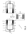
- the integrated optical waveguide evanescent field sensor 1 of figures 1A and 1B consists of a substrate 2 carrying a waveguide layer structure in the form of an input channel waveguide 3 that splits up in two parallel branches 4, 5. After a well-defined length, these two parallel branches 4, 5 are combined again to form the output waveguide 6. Light that enters the input waveguide 3 splits equally over the two branches 4, 5 and combines again at the output waveguide 6. Coupled to both the input channel waveguide 3 and the output waveguide 6 are optical fibers 7.
- the waveguide 3 and the two branches 4,5 comprise a waveguide core layer 10 sandwiched between two cladding layers formed by a lower cladding layer 11 and an upper cladding layer 12, of a lower refractive index than the waveguide core layer 10.
- the optical field is completely contained in the core and buffer layers and the propagation of light is not affected by environmental disturbances.
- the top cladding 12 is locally removed above the channel waveguides at well-defined positions in both branches 4, 5 of the sensor 1. In these so-called windows the evanescent field 16 of the light 17 that travels through the under-laying waveguides, extents into the environment above the sensor 1 and becomes susceptible to environmental changes.
- a sensing layer 13 that binds specifically with analyte molecules of interest is provided on the surface of the windows to form sensing sections 14A, 14B.
- sensing sections 14A, 14B When the sensing sections 14A, 14B are exposed to a sample material, specific binding of analyte molecules to the sensing layer 13 in the sensing sections 14A, 14B is probed by the evanescent field 16 of the light 17 travelling through the sensing branches 4, 5. This causes a change of the propagation speed of the light.
- the same analyte molecules may be sensed, thereby enhancing the accuracy, or different analyte molecules may be sensed, thereby having the opportunity to have multiple sensing at the same time.
- one of the sensing layers 13 in the sensing sections 14A, 14B of branches 4, 5 show no specific binding, such that this branch may act as a reference branch. Because no specific binding occurs in the reference branch, the propagation speed of the light does not change, thus resulting in a phase difference between light coming from the sensing branch and the reference branch at the output waveguide 7. The induced phase difference is proportional to the amount of analyte molecules binding to the sensing layer 13.
- a longitudinal section of said substrate 2 including said branches 4, 5 and said sensing sections 14A, 14B comprising said sensing layers 13 is exchangeable as a separate element 20.
- Said separate element 20 can be displaced between the position shown in figure 1A wherein the element 20 is separate from the sensor 1 and the position shown in figure 1A wherein the element 20 is located near a midzone of said sensor 1.
- the midzone is to be understood such that the separate element 20 is placed between two parts of the sensor 1, such that said two parts of the sensor 1 extend at opposite endzones of the separate element 20.
- the separate element 20 does not necessarily have to be placed in the middle of the sensor 1.
- the element 20 For optimal sensing with the sensor 1, the element 20 must be positioned correctly with respect to the midzone of said sensor 1, such that the light travelling through the two branches 4, 5 will travel through the sensing sections 14A, 14B and the sensing layers 13.
- the correct positioning is relatively easy since the thicknesses of all layers on the substrate are known, such that the top surface of the upper cladding layer 12 of the sensor 1 can be used as a plane of reference for passive alignment.
- the branches 4, 5 are only formed as channels over a part of said sensor 1, such that beams of light leaving the endzones 21, 22 of the channels will diverge.
- Two lenses 23 are included in the branches 4, 5 at locations outside the channels and outside the element 20, such that in use the two diverging beams leaving the two channels and passing through respective lenses 23 are converted into parallel beams 24, 25, which parallel beams 24, 25 have a width that is larger than the width of the channels. Due to the increased width of the beams, a correct position of the element 20 wherein the beam will travel through the sensing sections 14A, 14B and the sensing layers 13 is provided.
- Third and fourth lenses 26 are included in the branches 4, 5 at the other end of the sensor 1 at locations outside the channels and outside the separate element 20, such that in use the two parallel beams passing through respective lenses 26 are converted into converging beams entering the channels of the branches 4, 5.
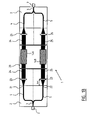
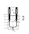
- Figures 2A and 2B show another preferred embodiment of the sensor 1 wherein the separate element 20 can be displaced between the position shown in figure 2A wherein the element 20 is separate from the sensor 1 and the position shown in figure 2B wherein the element 20 is located near an endzone of said sensor 1.
- the endzone is to be understood such that the separate element 20 is placed near one endzone of said sensor 1, such that the other endzone of the separate element 20 is the end of said sensor 1.
- light leaving the separate element 20 is not guided into another part of the sensor 1 as is the case with the sensor 1 of figures 1A , 1B .
- the light leaving the sensor may be directed on a CCD camera such as in a Young interferometer or focussed on a light detector using an external lens.
- the core layer 10 has an increased thickness with respect to the core layer 10 of figure 3 .
- This increased thickness makes positioning of the separate element 20 easier.
- Figure 4 also shows that the profile 18 of the light 17 does not change in the transfer to the separate element 20.
- the part 16 of the light 17 extending into the sensing layer 13 is relatively small. Therefore, the preferred embodiment of the sensor 1 of figure 4 has a second core layer 30 included in the first core layer 10 in the separate element 20, which second core layer 30 has tapered endzones 31, 32.
- the part 16 of the light 17 extending into the sensing layer 13 is increased due to the smaller thickness of the second core layer 30. Due to the tapered endzones 31, 32, the light 17 is effectively guided into the second core layer 30.
- Figure 5 shows another preferred embodiment of the sensor 1, wherein the coupling of the light travelling through the branches 4, 5 into the separate element 20 is enhanced.
- the lower cladding layer 11 of the separate element 20 of this preferred embodiment of the sensor 1 has a refractive index that is lower than the refractive index of the upper cladding layer 12 and the sensing layer 13. Due to this lower cladding layer 11 with a lower refractive index, the light 17 is effectively guided into the core layer 10 of the separate element 20, because the profile 19 of the light 17 extending into the upper cladding layer 12 remains more or less the same.
- the evanescent field extending into the sensing layers 13 is increased as compared to a sensor wherein the upper and lower cladding layers have the same refractive index or wherein the upper cladding layer has a refractive index that is higher. Due to the increased evanescent field extending into the sensing layers 13 the accuracy of the sensing is improved.
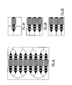
- Figures 6A and 6B show two configurations of a sensor which do not form part of the invention but represent background art that is useful for understanding the invention.
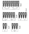
- FIGS 6C-T show several configurations of the sensor according to preferred embodiment of the invention. As appears from these figures, many configurations are possible. Therefore, it is clear that that these figures are not exclusive. Further, it is clear that all these possible configurations and/or not shown configurations fall within the scope of the appended claims. For clarity, the elements are numbered only in figures 6A-6C .
- Figure 6A shows a configuration wherein the waveguide layer structure 40 is formed as a single path, which path has a width that is larger than the width of the channels shown in figures 1 and 2 .
- Figure 6B shows a configuration wherein the waveguide layer structure 40 is formed as a channel over a portion of its length. This is a cheap and simple configuration of the sensor which does also not form part of the invention, because no lenses are needed.
- Figure 6C shows a configuration wherein the waveguide layer structure 40 is formed as a channel over a portion of its length.
- the sensor comprises an array of two lenses 23.
- An array of two or more lenses has the advantage that the diffraction losses are lower as compared to a single lens with the same power.
- Figures 6D-6L show a plurality of configurations wherein the waveguide layer structure 40 is formed as multiple paths and/or channels. Multiple paths and/or channels have the advantages of multiple analyzing, improving the accuracy, or having a reference path or channel as described before.
- Figures 6M-6T show a plurality of configurations wherein the separate element is located near an endzone of the sensor.
Landscapes
- Physics & Mathematics (AREA)
- Chemical & Material Sciences (AREA)
- General Health & Medical Sciences (AREA)
- Health & Medical Sciences (AREA)
- Life Sciences & Earth Sciences (AREA)
- Analytical Chemistry (AREA)
- Biochemistry (AREA)
- General Physics & Mathematics (AREA)
- Immunology (AREA)
- Pathology (AREA)
- Chemical Kinetics & Catalysis (AREA)
- Plasma & Fusion (AREA)
- Engineering & Computer Science (AREA)
- Investigating Or Analysing Materials By Optical Means (AREA)
- Optical Integrated Circuits (AREA)
Claims (10)
- Integrierter Lichtwellenleiter-Evaneszenzfeldsensor (1) zum Erfassen von chemischen und/oder physikalischen Größen, aufweisend ein Substrat (2), das eine Wellenleiterschichtstruktur trägt, aufweisend:- eine Wellenleiterkernschicht (10), eingelegt zwischen zwei Mantelschichten (11, 12), die durch eine untere (11) und eine obere (12) Mantelschicht mit einem niedrigeren Brechungsindex als die Wellenleiterkernschicht (10) ausgebildet sind,- einen Erfassungsabschnitt (14A, 14B), aufweisend eine Erfassungsschicht (13), die in der oberen Mantelschicht (12) umfasst ist,wobei die Wellenleiterschichtstruktur über einen Teil ihrer Länge als ein Kanal (4, 5) ausgebildet ist,
wobei ein longitudinaler Abschnitt des Substrats, der die Wellenleiterschichtstruktur und den Erfassungsabschnitt umfasst, als separates Element (20) austauschbar ist,
dadurch gekennzeichnet, dass wenigstens eine Linse (23) in der Wellenleiterschichtstruktur enthalten ist, angeordnet außerhalb des Kanals (4, 5) und außerhalb des separaten Elements (20), so dass bei Verwendung ein divergenter Strahl, der den Kanal (4, 5) verlässt und durch die Linse (23) hindurchläuft, in einen parallelen Strahl (24, 25) umgewandelt wird, wobei der parallele Strahl (24, 25) eine Breite aufweist, die größer ist als die Breite des Kanals (4, 5). - Integrierter Lichtwellenleiter-Evaneszenzfeldsensor (1) nach Anspruch 1, wobei das separate Element (20) nahe eines Mittelbereichs oder eines Endbereichs des Sensors (1) angeordnet sein kann.
- Integrierter Lichtwellenleiter-Evaneszenzfeldsensor (1) nach einem der vorstehenden Ansprüche 1-2, wobei die Wellenleiterschichtstruktur über besagten Teil ihrer Länge als zwei parallele Kanäle (4, 5) ausgebildet ist, wobei zwei Linsen (23) in der Wellenleiterschichtstruktur umfasst sind, angeordnet außerhalb der Kanäle (4, 5) und außerhalb des separaten Elements (20), so dass bei Verwendung zwei divergente Strahlen , die die zwei Kanäle (4, 5) verlassen und durch die entsprechenden Linsen (23) hindurchlaufen, in parallele Strahlen (24, 25) umgewandelt werden, wobei die parallelen Strahlen (24, 25) eine Breite aufweisen, die größer ist als die Breite der Kanäle (4, 5).
- Integrierter Lichtwellenleiter-Evaneszenzfeldsensor (1) nach Anspruch 3, wobei das Substrat (2) an einer ersten Verzweigung einen Splitter zum optischen Splitten eines gemeinsamen Eingangskanals (3) in die ersten und zweiten Kanäle (4, 5) aufweist.
- Integrierter Lichtwellenleiter-Evaneszenzfeldsensor (1) nach Anspruch 3 oder 4, wobei die Wellenleiterschichtstruktur über einen zweiten Teil ihrer Länge als zwei parallele dritte und vierte Kanäle (4, 5) ausgebildet ist, wobei eine dritte Linse (26) und eine vierte Linse (26) in der Wellenleiterschichtstruktur umfasst sind, angeordnet außerhalb der Kanäle (4, 5) und außerhalb des separaten Elements (20), so dass bei Verwendung die zwei parallelen Strahlen, die durch die jeweiligen Linsen (26) hindurchlaufen, in konvergente Strahlen umgewandelt werden, die in den dritten und vierten Kanal (4, 5) einlaufen.
- Integrierter Lichtwellenleiter-Evaneszenzfeldsensor (1) nach Anspruch 5, bei dem das Substrat (2) an einer zweiten Verzweigung einen Kombinator zum optischen Koppeln des dritten und vierten Kanals (4, 5) in einen gemeinsamen Ausgangskanal (6) aufweist.
- Integrierter Lichtwellenleiter-Evaneszenzfeldsensor (1) nach einem der vorstehenden Ansprüche 1-6, wobei die Kernschicht (10) im separaten Element (20) eine zweite Kernschicht (30) mit konischem Endbereichen (31, 32) umfasst.
- Integrierter Lichtwellenleiter-Evaneszenzfeldsensor (1) nach einem der vorstehenden Ansprüche 1-7, bei dem die untere Mantelschicht (11) des wenigstens einen separaten Elements (20) einen Brechungsindex aufweist, der niedriger ist als der Brechungsindex der oberen Mantelschicht (12) und/oder der Erfassungsschicht (13).
- Integrierter Lichtwellenleiter-Evaneszenzfeldsensor (1) nach einem der vorstehenden Ansprüche 1-8, bei dem das Substrat (2) durch die untere Mantelschicht (11) als ein integrales Teil ausgebildet ist.
- Longitudinaler Abschnitt eines Substrats (2), eingerichtet, um als ein austauschbares separates Element (20) in einem integrierten Lichtwellenleiter-Evaneszenzfeldsensor (1) zum Erfassen von chemischen und/oder physikalischen Größen nach einem der vorstehenden Ansprüche 1-9 verwendet zu werden, wobei der Sensor (1) ein Substrat (2) aufweist, das eine Wellenleiterschichtstruktur trägt, ausgestattet mit:- einer Wellenleiterkernschicht (10), eingelegt zwischen zwei Mantelschichten (11, 12), die durch eine untere (11) und eine obere (12) Mantelschicht mit einem niedrigeren Brechungsindex als die Wellenleiterkernschicht (10) ausgebildet sind,- einen Erfassungsabschnitt (14A, 14B), aufweisend eine Erfassungsschicht (13), die in der oberen Mantelschicht (12) umfasst ist,wobei die Wellenleiterschichtstruktur über einen Teil ihrer Länge als ein Kanal (4, 5) ausgebildet ist,
wobei der longitudinale Abschnitt des Substrats, der die Wellenleiterschichtstruktur und den Erfassungsabschnitt umfasst, als separates Element (20) austauschbar ist,
dadurch gekennzeichnet, dass wenigstens eine Linse (23) in der Wellenleiterschichtstruktur enthalten ist, angeordnet außerhalb des Kanals (4, 5) und außerhalb des separaten Elements (20), so dass bei Verwendung ein divergenter Strahl, der den Kanal (4, 5) verlässt und durch die Linse (23) hindurchläuft, in einen parallelen Strahl (24, 25) umgewandelt wird, wobei der parallele Strahl (24, 25) eine Breite aufweist, die größer ist als die Breite des Kanals (4, 5), und
wobei die Wellenleiterschichtstruktur (10) des separaten Elements (20) im Wesentlichen planar vorgesehen ist.
Priority Applications (1)
| Application Number | Priority Date | Filing Date | Title |
|---|---|---|---|
| EP11725096.9A EP2583086B1 (de) | 2010-06-17 | 2011-06-15 | Integrierter Lichtwellenleiter-Evaneszenzfeldsensor |
Applications Claiming Priority (3)
| Application Number | Priority Date | Filing Date | Title |
|---|---|---|---|
| EP10166404A EP2400291A1 (de) | 2010-06-17 | 2010-06-17 | Integrierter Lichtwellenleiter-Evaneszenzfeldsensor und länglicher Abschnitt eines Substrats zur Verwendung in solch einem Sensor |
| EP11725096.9A EP2583086B1 (de) | 2010-06-17 | 2011-06-15 | Integrierter Lichtwellenleiter-Evaneszenzfeldsensor |
| PCT/EP2011/059971 WO2011157766A1 (en) | 2010-06-17 | 2011-06-15 | Integrated optical waveguide evanescent field sensor and longitudinal section of a substrate for use in such a sensor |
Publications (2)
| Publication Number | Publication Date |
|---|---|
| EP2583086A1 EP2583086A1 (de) | 2013-04-24 |
| EP2583086B1 true EP2583086B1 (de) | 2015-11-11 |
Family
ID=42341462
Family Applications (2)
| Application Number | Title | Priority Date | Filing Date |
|---|---|---|---|
| EP10166404A Withdrawn EP2400291A1 (de) | 2010-06-17 | 2010-06-17 | Integrierter Lichtwellenleiter-Evaneszenzfeldsensor und länglicher Abschnitt eines Substrats zur Verwendung in solch einem Sensor |
| EP11725096.9A Not-in-force EP2583086B1 (de) | 2010-06-17 | 2011-06-15 | Integrierter Lichtwellenleiter-Evaneszenzfeldsensor |
Family Applications Before (1)
| Application Number | Title | Priority Date | Filing Date |
|---|---|---|---|
| EP10166404A Withdrawn EP2400291A1 (de) | 2010-06-17 | 2010-06-17 | Integrierter Lichtwellenleiter-Evaneszenzfeldsensor und länglicher Abschnitt eines Substrats zur Verwendung in solch einem Sensor |
Country Status (4)
| Country | Link |
|---|---|
| US (1) | US8971672B2 (de) |
| EP (2) | EP2400291A1 (de) |
| CN (1) | CN103026209B (de) |
| WO (1) | WO2011157766A1 (de) |
Families Citing this family (11)
| Publication number | Priority date | Publication date | Assignee | Title |
|---|---|---|---|---|
| DE102012222039A1 (de) * | 2012-12-03 | 2014-06-05 | Fraunhofer-Gesellschaft zur Förderung der angewandten Forschung e.V. | Interferometrische Messzelle, Spektrometer und Verfahren zur spektroskopischen Messung |
| WO2016086043A1 (en) | 2014-11-24 | 2016-06-02 | Massachusetts Institute Of Technology | Methods and apparatus for spectral imaging |
| WO2017019482A1 (en) | 2015-07-24 | 2017-02-02 | Massachusetts Institute Of Technology | Apparatus, systems, and methods for biomedical imaging and stimulation |
| US10006809B2 (en) | 2016-02-10 | 2018-06-26 | Massachusetts Institute Of Technology | Apparatus, systems, and methods for on-chip spectroscopy using optical switches |
| US10718668B2 (en) | 2017-08-08 | 2020-07-21 | Massachusetts Institute Of Technology | Miniaturized Fourier-transform Raman spectrometer systems and methods |
| US11041759B2 (en) | 2018-06-28 | 2021-06-22 | Massachusetts Institute Of Technology | Systems and methods for Raman spectroscopy |
| US10983003B2 (en) | 2019-02-11 | 2021-04-20 | Massachusetts Institute Of Technology | High-performance on-chip spectrometers and spectrum analyzers |
| FR3097640B1 (fr) * | 2019-06-21 | 2021-07-02 | Commissariat Energie Atomique | Circuit optique intégré à bras de référence encapsulé |
| WO2022258559A1 (fr) * | 2021-06-10 | 2022-12-15 | Commissariat A L'energie Atomique Et Aux Energies Alternatives | Systeme interferometrique de detection d'analytes comportant une matrice d'interferometres de mach-zehnder |
| CN115047564A (zh) * | 2022-05-18 | 2022-09-13 | 上海图灵智算量子科技有限公司 | 具有渐缩表面的波导 |
| CN115406863B (zh) * | 2022-08-31 | 2025-01-28 | 西安电子科技大学杭州研究院 | 一种集成光波导生物传感器及其制作方法 |
Family Cites Families (9)
| Publication number | Priority date | Publication date | Assignee | Title |
|---|---|---|---|---|
| US5173747A (en) * | 1990-09-20 | 1992-12-22 | Battelle Memorial Institute | Integrated optical directional-coupling refractometer apparatus |
| JP2004354068A (ja) * | 2003-05-27 | 2004-12-16 | Hitachi Ltd | 光導波路を用いた化学物質計測装置 |
| US20050201660A1 (en) * | 2004-03-11 | 2005-09-15 | Grot Annette C. | Apparatus for single nanoparticle detection |
| US7233711B1 (en) * | 2005-05-11 | 2007-06-19 | Hewlett Packard Development Company, L.P. | Autonomous evanescent optical nanosensor |
| US8288157B2 (en) * | 2007-09-12 | 2012-10-16 | Plc Diagnostics, Inc. | Waveguide-based optical scanning systems |
| US7389025B2 (en) * | 2006-03-29 | 2008-06-17 | 3M Innovative Properties Company | Coupling light into microresonators |
| US20080101744A1 (en) * | 2006-10-31 | 2008-05-01 | Honeywell International Inc. | Optical Waveguide Sensor Devices and Methods For Making and Using Them |
| WO2008096296A1 (en) * | 2007-02-08 | 2008-08-14 | Koninklijke Philips Electronics N.V. | Biosensor with evanescent waveguide and integrated sensor |
| DK3629011T3 (da) * | 2008-09-16 | 2024-01-29 | Pacific Biosciences California Inc | Integreret optisk indretning |
-
2010
- 2010-06-17 EP EP10166404A patent/EP2400291A1/de not_active Withdrawn
-
2011
- 2011-06-15 EP EP11725096.9A patent/EP2583086B1/de not_active Not-in-force
- 2011-06-15 US US13/704,509 patent/US8971672B2/en not_active Expired - Fee Related
- 2011-06-15 CN CN201180033484.4A patent/CN103026209B/zh not_active Expired - Fee Related
- 2011-06-15 WO PCT/EP2011/059971 patent/WO2011157766A1/en not_active Ceased
Also Published As
| Publication number | Publication date |
|---|---|
| CN103026209A (zh) | 2013-04-03 |
| EP2400291A1 (de) | 2011-12-28 |
| US20130156363A1 (en) | 2013-06-20 |
| EP2583086A1 (de) | 2013-04-24 |
| CN103026209B (zh) | 2015-11-25 |
| US8971672B2 (en) | 2015-03-03 |
| WO2011157766A1 (en) | 2011-12-22 |
Similar Documents
| Publication | Publication Date | Title |
|---|---|---|
| US8971672B2 (en) | Integrated optical waveguide evanescent field sensor and longitudinal section of a substrate for use in such a sensor | |
| US10487356B2 (en) | Integrated devices and systems for free-space optical coupling | |
| US8620120B2 (en) | Retro-reflective structures | |
| US20130142477A1 (en) | Integrated optical waveguide evanscent field sensor | |
| US20100165351A1 (en) | Silicon photonic waveguide biosensor configurations | |
| CN110945316B (zh) | 用于检查样品的多通道共焦传感器和相关方法 | |
| CA2600621A1 (en) | Multi-core strain compensated optical fiber temperature sensor | |
| AU2018221428A1 (en) | Integrated plasmo-photonic biosensor and method of use | |
| JP2005009944A (ja) | 化学物質検出装置 | |
| TWI877603B (zh) | 透過波長路徑區劃於晶圓級測試測量光損耗之方法以及系統 | |
| JP6817180B2 (ja) | ディスポーザブル生化学センサ装置 | |
| CA2696010A1 (en) | Interferometer and sensor based on bimodal optical waveguide and sensing method | |
| JP2025515831A5 (de) | ||
| KR20220082268A (ko) | 광 도파로 기반 분광기 | |
| JP4770449B2 (ja) | 光導波路型デバイス、温度計測装置および温度計測方法 | |
| HK40111630A (zh) | 通过波长路径划分测量晶片级测试中光损耗的方法和系统 | |
| Helmers et al. | Integrated optical components employing slab waveguides for sensor applications | |
| CN120927615A (zh) | 一种基于周期串联侧抛光子晶体光纤结构的多点折射率测量光纤传感器 | |
| Densmore et al. | Integration of vertical grating couplers and microfluidic channels with silicon photonic wire biosensor arrays | |
| EP2400289A1 (de) | Integrierter Lichtwellenleiter-Evaneszenzfeldsensor |
Legal Events
| Date | Code | Title | Description |
|---|---|---|---|
| PUAI | Public reference made under article 153(3) epc to a published international application that has entered the european phase |
Free format text: ORIGINAL CODE: 0009012 |
|
| 17P | Request for examination filed |
Effective date: 20130114 |
|
| AK | Designated contracting states |
Kind code of ref document: A1 Designated state(s): AL AT BE BG CH CY CZ DE DK EE ES FI FR GB GR HR HU IE IS IT LI LT LU LV MC MK MT NL NO PL PT RO RS SE SI SK SM TR |
|
| DAX | Request for extension of the european patent (deleted) | ||
| GRAP | Despatch of communication of intention to grant a patent |
Free format text: ORIGINAL CODE: EPIDOSNIGR1 |
|
| RIC1 | Information provided on ipc code assigned before grant |
Ipc: G01N 21/77 20060101AFI20141204BHEP |
|
| INTG | Intention to grant announced |
Effective date: 20141218 |
|
| GRAP | Despatch of communication of intention to grant a patent |
Free format text: ORIGINAL CODE: EPIDOSNIGR1 |
|
| RIC1 | Information provided on ipc code assigned before grant |
Ipc: G01N 21/77 20060101AFI20150526BHEP |
|
| INTG | Intention to grant announced |
Effective date: 20150619 |
|
| GRAS | Grant fee paid |
Free format text: ORIGINAL CODE: EPIDOSNIGR3 |
|
| GRAA | (expected) grant |
Free format text: ORIGINAL CODE: 0009210 |
|
| AK | Designated contracting states |
Kind code of ref document: B1 Designated state(s): AL AT BE BG CH CY CZ DE DK EE ES FI FR GB GR HR HU IE IS IT LI LT LU LV MC MK MT NL NO PL PT RO RS SE SI SK SM TR |
|
| REG | Reference to a national code |
Ref country code: GB Ref legal event code: FG4D |
|
| REG | Reference to a national code |
Ref country code: CH Ref legal event code: EP |
|
| REG | Reference to a national code |
Ref country code: IE Ref legal event code: FG4D |
|
| REG | Reference to a national code |
Ref country code: AT Ref legal event code: REF Ref document number: 760703 Country of ref document: AT Kind code of ref document: T Effective date: 20151215 |
|
| REG | Reference to a national code |
Ref country code: DE Ref legal event code: R096 Ref document number: 602011021380 Country of ref document: DE |
|
| REG | Reference to a national code |
Ref country code: LT Ref legal event code: MG4D |
|
| REG | Reference to a national code |
Ref country code: NL Ref legal event code: MP Effective date: 20160211 |
|
| REG | Reference to a national code |
Ref country code: AT Ref legal event code: MK05 Ref document number: 760703 Country of ref document: AT Kind code of ref document: T Effective date: 20151111 |
|
| PG25 | Lapsed in a contracting state [announced via postgrant information from national office to epo] |
Ref country code: IS Free format text: LAPSE BECAUSE OF FAILURE TO SUBMIT A TRANSLATION OF THE DESCRIPTION OR TO PAY THE FEE WITHIN THE PRESCRIBED TIME-LIMIT Effective date: 20160311 Ref country code: NL Free format text: LAPSE BECAUSE OF FAILURE TO SUBMIT A TRANSLATION OF THE DESCRIPTION OR TO PAY THE FEE WITHIN THE PRESCRIBED TIME-LIMIT Effective date: 20151111 Ref country code: NO Free format text: LAPSE BECAUSE OF FAILURE TO SUBMIT A TRANSLATION OF THE DESCRIPTION OR TO PAY THE FEE WITHIN THE PRESCRIBED TIME-LIMIT Effective date: 20160211 Ref country code: HR Free format text: LAPSE BECAUSE OF FAILURE TO SUBMIT A TRANSLATION OF THE DESCRIPTION OR TO PAY THE FEE WITHIN THE PRESCRIBED TIME-LIMIT Effective date: 20151111 Ref country code: LT Free format text: LAPSE BECAUSE OF FAILURE TO SUBMIT A TRANSLATION OF THE DESCRIPTION OR TO PAY THE FEE WITHIN THE PRESCRIBED TIME-LIMIT Effective date: 20151111 Ref country code: ES Free format text: LAPSE BECAUSE OF FAILURE TO SUBMIT A TRANSLATION OF THE DESCRIPTION OR TO PAY THE FEE WITHIN THE PRESCRIBED TIME-LIMIT Effective date: 20151111 Ref country code: IT Free format text: LAPSE BECAUSE OF FAILURE TO SUBMIT A TRANSLATION OF THE DESCRIPTION OR TO PAY THE FEE WITHIN THE PRESCRIBED TIME-LIMIT Effective date: 20151111 |
|
| PG25 | Lapsed in a contracting state [announced via postgrant information from national office to epo] |
Ref country code: FI Free format text: LAPSE BECAUSE OF FAILURE TO SUBMIT A TRANSLATION OF THE DESCRIPTION OR TO PAY THE FEE WITHIN THE PRESCRIBED TIME-LIMIT Effective date: 20151111 Ref country code: LV Free format text: LAPSE BECAUSE OF FAILURE TO SUBMIT A TRANSLATION OF THE DESCRIPTION OR TO PAY THE FEE WITHIN THE PRESCRIBED TIME-LIMIT Effective date: 20151111 Ref country code: RS Free format text: LAPSE BECAUSE OF FAILURE TO SUBMIT A TRANSLATION OF THE DESCRIPTION OR TO PAY THE FEE WITHIN THE PRESCRIBED TIME-LIMIT Effective date: 20151111 Ref country code: SE Free format text: LAPSE BECAUSE OF FAILURE TO SUBMIT A TRANSLATION OF THE DESCRIPTION OR TO PAY THE FEE WITHIN THE PRESCRIBED TIME-LIMIT Effective date: 20151111 Ref country code: PL Free format text: LAPSE BECAUSE OF FAILURE TO SUBMIT A TRANSLATION OF THE DESCRIPTION OR TO PAY THE FEE WITHIN THE PRESCRIBED TIME-LIMIT Effective date: 20151111 Ref country code: PT Free format text: LAPSE BECAUSE OF FAILURE TO SUBMIT A TRANSLATION OF THE DESCRIPTION OR TO PAY THE FEE WITHIN THE PRESCRIBED TIME-LIMIT Effective date: 20160311 Ref country code: GR Free format text: LAPSE BECAUSE OF FAILURE TO SUBMIT A TRANSLATION OF THE DESCRIPTION OR TO PAY THE FEE WITHIN THE PRESCRIBED TIME-LIMIT Effective date: 20160212 Ref country code: AT Free format text: LAPSE BECAUSE OF FAILURE TO SUBMIT A TRANSLATION OF THE DESCRIPTION OR TO PAY THE FEE WITHIN THE PRESCRIBED TIME-LIMIT Effective date: 20151111 |
|
| PG25 | Lapsed in a contracting state [announced via postgrant information from national office to epo] |
Ref country code: CZ Free format text: LAPSE BECAUSE OF FAILURE TO SUBMIT A TRANSLATION OF THE DESCRIPTION OR TO PAY THE FEE WITHIN THE PRESCRIBED TIME-LIMIT Effective date: 20151111 |
|
| REG | Reference to a national code |
Ref country code: DE Ref legal event code: R097 Ref document number: 602011021380 Country of ref document: DE |
|
| PG25 | Lapsed in a contracting state [announced via postgrant information from national office to epo] |
Ref country code: EE Free format text: LAPSE BECAUSE OF FAILURE TO SUBMIT A TRANSLATION OF THE DESCRIPTION OR TO PAY THE FEE WITHIN THE PRESCRIBED TIME-LIMIT Effective date: 20151111 Ref country code: RO Free format text: LAPSE BECAUSE OF FAILURE TO SUBMIT A TRANSLATION OF THE DESCRIPTION OR TO PAY THE FEE WITHIN THE PRESCRIBED TIME-LIMIT Effective date: 20151111 Ref country code: SK Free format text: LAPSE BECAUSE OF FAILURE TO SUBMIT A TRANSLATION OF THE DESCRIPTION OR TO PAY THE FEE WITHIN THE PRESCRIBED TIME-LIMIT Effective date: 20151111 Ref country code: SM Free format text: LAPSE BECAUSE OF FAILURE TO SUBMIT A TRANSLATION OF THE DESCRIPTION OR TO PAY THE FEE WITHIN THE PRESCRIBED TIME-LIMIT Effective date: 20151111 Ref country code: DK Free format text: LAPSE BECAUSE OF FAILURE TO SUBMIT A TRANSLATION OF THE DESCRIPTION OR TO PAY THE FEE WITHIN THE PRESCRIBED TIME-LIMIT Effective date: 20151111 |
|
| PLBE | No opposition filed within time limit |
Free format text: ORIGINAL CODE: 0009261 |
|
| STAA | Information on the status of an ep patent application or granted ep patent |
Free format text: STATUS: NO OPPOSITION FILED WITHIN TIME LIMIT |
|
| 26N | No opposition filed |
Effective date: 20160812 |
|
| PG25 | Lapsed in a contracting state [announced via postgrant information from national office to epo] |
Ref country code: SI Free format text: LAPSE BECAUSE OF FAILURE TO SUBMIT A TRANSLATION OF THE DESCRIPTION OR TO PAY THE FEE WITHIN THE PRESCRIBED TIME-LIMIT Effective date: 20151111 |
|
| PG25 | Lapsed in a contracting state [announced via postgrant information from national office to epo] |
Ref country code: BE Free format text: LAPSE BECAUSE OF FAILURE TO SUBMIT A TRANSLATION OF THE DESCRIPTION OR TO PAY THE FEE WITHIN THE PRESCRIBED TIME-LIMIT Effective date: 20151111 |
|
| REG | Reference to a national code |
Ref country code: DE Ref legal event code: R119 Ref document number: 602011021380 Country of ref document: DE |
|
| PG25 | Lapsed in a contracting state [announced via postgrant information from national office to epo] |
Ref country code: MC Free format text: LAPSE BECAUSE OF FAILURE TO SUBMIT A TRANSLATION OF THE DESCRIPTION OR TO PAY THE FEE WITHIN THE PRESCRIBED TIME-LIMIT Effective date: 20151111 |
|
| REG | Reference to a national code |
Ref country code: CH Ref legal event code: PL |
|
| GBPC | Gb: european patent ceased through non-payment of renewal fee |
Effective date: 20160615 |
|
| REG | Reference to a national code |
Ref country code: IE Ref legal event code: MM4A |
|
| REG | Reference to a national code |
Ref country code: FR Ref legal event code: ST Effective date: 20170228 |
|
| PG25 | Lapsed in a contracting state [announced via postgrant information from national office to epo] |
Ref country code: CH Free format text: LAPSE BECAUSE OF NON-PAYMENT OF DUE FEES Effective date: 20160630 Ref country code: LI Free format text: LAPSE BECAUSE OF NON-PAYMENT OF DUE FEES Effective date: 20160630 Ref country code: FR Free format text: LAPSE BECAUSE OF NON-PAYMENT OF DUE FEES Effective date: 20160630 Ref country code: DE Free format text: LAPSE BECAUSE OF NON-PAYMENT OF DUE FEES Effective date: 20170103 |
|
| PG25 | Lapsed in a contracting state [announced via postgrant information from national office to epo] |
Ref country code: GB Free format text: LAPSE BECAUSE OF NON-PAYMENT OF DUE FEES Effective date: 20160615 Ref country code: IE Free format text: LAPSE BECAUSE OF NON-PAYMENT OF DUE FEES Effective date: 20160615 |
|
| PG25 | Lapsed in a contracting state [announced via postgrant information from national office to epo] |
Ref country code: HU Free format text: LAPSE BECAUSE OF FAILURE TO SUBMIT A TRANSLATION OF THE DESCRIPTION OR TO PAY THE FEE WITHIN THE PRESCRIBED TIME-LIMIT; INVALID AB INITIO Effective date: 20110615 Ref country code: CY Free format text: LAPSE BECAUSE OF FAILURE TO SUBMIT A TRANSLATION OF THE DESCRIPTION OR TO PAY THE FEE WITHIN THE PRESCRIBED TIME-LIMIT Effective date: 20151111 |
|
| PG25 | Lapsed in a contracting state [announced via postgrant information from national office to epo] |
Ref country code: MT Free format text: LAPSE BECAUSE OF NON-PAYMENT OF DUE FEES Effective date: 20160630 Ref country code: TR Free format text: LAPSE BECAUSE OF FAILURE TO SUBMIT A TRANSLATION OF THE DESCRIPTION OR TO PAY THE FEE WITHIN THE PRESCRIBED TIME-LIMIT Effective date: 20151111 Ref country code: MK Free format text: LAPSE BECAUSE OF FAILURE TO SUBMIT A TRANSLATION OF THE DESCRIPTION OR TO PAY THE FEE WITHIN THE PRESCRIBED TIME-LIMIT Effective date: 20151111 Ref country code: LU Free format text: LAPSE BECAUSE OF NON-PAYMENT OF DUE FEES Effective date: 20160615 |
|
| PG25 | Lapsed in a contracting state [announced via postgrant information from national office to epo] |
Ref country code: BG Free format text: LAPSE BECAUSE OF FAILURE TO SUBMIT A TRANSLATION OF THE DESCRIPTION OR TO PAY THE FEE WITHIN THE PRESCRIBED TIME-LIMIT Effective date: 20151111 |
|
| PG25 | Lapsed in a contracting state [announced via postgrant information from national office to epo] |
Ref country code: AL Free format text: LAPSE BECAUSE OF FAILURE TO SUBMIT A TRANSLATION OF THE DESCRIPTION OR TO PAY THE FEE WITHIN THE PRESCRIBED TIME-LIMIT Effective date: 20151111 |