EP2581958A2 - Organic light emitting diode display and method for manufacturing the same - Google Patents
Organic light emitting diode display and method for manufacturing the same Download PDFInfo
- Publication number
- EP2581958A2 EP2581958A2 EP12188295.5A EP12188295A EP2581958A2 EP 2581958 A2 EP2581958 A2 EP 2581958A2 EP 12188295 A EP12188295 A EP 12188295A EP 2581958 A2 EP2581958 A2 EP 2581958A2
- Authority
- EP
- European Patent Office
- Prior art keywords
- layer
- inorganic layer
- inorganic
- light emitting
- emitting diode
- Prior art date
- Legal status (The legal status is an assumption and is not a legal conclusion. Google has not performed a legal analysis and makes no representation as to the accuracy of the status listed.)
- Ceased
Links
- 238000000034 method Methods 0.000 title claims abstract description 35
- 238000004519 manufacturing process Methods 0.000 title claims description 29
- 239000000758 substrate Substances 0.000 claims abstract description 48
- 238000000231 atomic layer deposition Methods 0.000 claims abstract description 30
- 239000010410 layer Substances 0.000 claims description 330
- 239000012044 organic layer Substances 0.000 claims description 24
- 229910044991 metal oxide Inorganic materials 0.000 claims description 12
- 150000004706 metal oxides Chemical class 0.000 claims description 12
- 239000010409 thin film Substances 0.000 description 42
- 238000005538 encapsulation Methods 0.000 description 41
- QVGXLLKOCUKJST-UHFFFAOYSA-N atomic oxygen Chemical compound [O] QVGXLLKOCUKJST-UHFFFAOYSA-N 0.000 description 19
- 229910052760 oxygen Inorganic materials 0.000 description 19
- 239000001301 oxygen Substances 0.000 description 19
- 230000000052 comparative effect Effects 0.000 description 17
- 239000011229 interlayer Substances 0.000 description 15
- 230000008569 process Effects 0.000 description 13
- 239000000463 material Substances 0.000 description 12
- 238000002474 experimental method Methods 0.000 description 8
- 239000004065 semiconductor Substances 0.000 description 8
- VYPSYNLAJGMNEJ-UHFFFAOYSA-N silicon dioxide Inorganic materials O=[Si]=O VYPSYNLAJGMNEJ-UHFFFAOYSA-N 0.000 description 8
- 229910052814 silicon oxide Inorganic materials 0.000 description 8
- 229910052581 Si3N4 Inorganic materials 0.000 description 6
- 238000009413 insulation Methods 0.000 description 6
- 230000004888 barrier function Effects 0.000 description 5
- GWEVSGVZZGPLCZ-UHFFFAOYSA-N Titan oxide Chemical compound O=[Ti]=O GWEVSGVZZGPLCZ-UHFFFAOYSA-N 0.000 description 4
- -1 acryl Chemical group 0.000 description 4
- 238000000151 deposition Methods 0.000 description 4
- 239000011521 glass Substances 0.000 description 4
- 229920000642 polymer Polymers 0.000 description 4
- 229920005989 resin Polymers 0.000 description 4
- 239000011347 resin Substances 0.000 description 4
- HQVNEWCFYHHQES-UHFFFAOYSA-N silicon nitride Chemical compound N12[Si]34N5[Si]62N3[Si]51N64 HQVNEWCFYHHQES-UHFFFAOYSA-N 0.000 description 4
- 230000001629 suppression Effects 0.000 description 4
- BOTDANWDWHJENH-UHFFFAOYSA-N Tetraethyl orthosilicate Chemical compound CCO[Si](OCC)(OCC)OCC BOTDANWDWHJENH-UHFFFAOYSA-N 0.000 description 3
- 238000012986 modification Methods 0.000 description 3
- 230000004048 modification Effects 0.000 description 3
- 239000002356 single layer Substances 0.000 description 3
- 239000004593 Epoxy Substances 0.000 description 2
- 239000004698 Polyethylene Substances 0.000 description 2
- GEIAQOFPUVMAGM-UHFFFAOYSA-N ZrO Inorganic materials [Zr]=O GEIAQOFPUVMAGM-UHFFFAOYSA-N 0.000 description 2
- 230000001133 acceleration Effects 0.000 description 2
- PNEYBMLMFCGWSK-UHFFFAOYSA-N aluminium oxide Inorganic materials [O-2].[O-2].[O-2].[Al+3].[Al+3] PNEYBMLMFCGWSK-UHFFFAOYSA-N 0.000 description 2
- 239000000919 ceramic Substances 0.000 description 2
- 239000004020 conductor Substances 0.000 description 2
- 229910052593 corundum Inorganic materials 0.000 description 2
- 238000002347 injection Methods 0.000 description 2
- 239000007924 injection Substances 0.000 description 2
- 229910010272 inorganic material Inorganic materials 0.000 description 2
- 239000011147 inorganic material Substances 0.000 description 2
- 229920000573 polyethylene Polymers 0.000 description 2
- 239000010453 quartz Substances 0.000 description 2
- PBCFLUZVCVVTBY-UHFFFAOYSA-N tantalum pentoxide Inorganic materials O=[Ta](=O)O[Ta](=O)=O PBCFLUZVCVVTBY-UHFFFAOYSA-N 0.000 description 2
- 229910001845 yogo sapphire Inorganic materials 0.000 description 2
- XLOMVQKBTHCTTD-UHFFFAOYSA-N zinc oxide Inorganic materials [Zn]=O XLOMVQKBTHCTTD-UHFFFAOYSA-N 0.000 description 2
- 229910017083 AlN Inorganic materials 0.000 description 1
- 229910017109 AlON Inorganic materials 0.000 description 1
- 206010030924 Optic ischaemic neuropathy Diseases 0.000 description 1
- 239000004952 Polyamide Substances 0.000 description 1
- 239000004642 Polyimide Substances 0.000 description 1
- 229910021417 amorphous silicon Inorganic materials 0.000 description 1
- 239000000470 constituent Substances 0.000 description 1
- 230000003247 decreasing effect Effects 0.000 description 1
- 238000010586 diagram Methods 0.000 description 1
- 238000011156 evaluation Methods 0.000 description 1
- 230000005283 ground state Effects 0.000 description 1
- 239000012774 insulation material Substances 0.000 description 1
- 239000004973 liquid crystal related substance Substances 0.000 description 1
- 229920002647 polyamide Polymers 0.000 description 1
- 229910021420 polycrystalline silicon Inorganic materials 0.000 description 1
- 229920001721 polyimide Polymers 0.000 description 1
- 229920005591 polysilicon Polymers 0.000 description 1
- 230000004044 response Effects 0.000 description 1
- 238000007789 sealing Methods 0.000 description 1
Images


Classifications
-
- H—ELECTRICITY
- H10—SEMICONDUCTOR DEVICES; ELECTRIC SOLID-STATE DEVICES NOT OTHERWISE PROVIDED FOR
- H10K—ORGANIC ELECTRIC SOLID-STATE DEVICES
- H10K59/00—Integrated devices, or assemblies of multiple devices, comprising at least one organic light-emitting element covered by group H10K50/00
- H10K59/80—Constructional details
- H10K59/87—Passivation; Containers; Encapsulations
- H10K59/873—Encapsulations
- H10K59/8731—Encapsulations multilayered coatings having a repetitive structure, e.g. having multiple organic-inorganic bilayers
-
- H—ELECTRICITY
- H10—SEMICONDUCTOR DEVICES; ELECTRIC SOLID-STATE DEVICES NOT OTHERWISE PROVIDED FOR
- H10K—ORGANIC ELECTRIC SOLID-STATE DEVICES
- H10K50/00—Organic light-emitting devices
- H10K50/80—Constructional details
- H10K50/84—Passivation; Containers; Encapsulations
- H10K50/844—Encapsulations
- H10K50/8445—Encapsulations multilayered coatings having a repetitive structure, e.g. having multiple organic-inorganic bilayers
-
- H—ELECTRICITY
- H10—SEMICONDUCTOR DEVICES; ELECTRIC SOLID-STATE DEVICES NOT OTHERWISE PROVIDED FOR
- H10K—ORGANIC ELECTRIC SOLID-STATE DEVICES
- H10K2102/00—Constructional details relating to the organic devices covered by this subclass
-
- H—ELECTRICITY
- H10—SEMICONDUCTOR DEVICES; ELECTRIC SOLID-STATE DEVICES NOT OTHERWISE PROVIDED FOR
- H10K—ORGANIC ELECTRIC SOLID-STATE DEVICES
- H10K59/00—Integrated devices, or assemblies of multiple devices, comprising at least one organic light-emitting element covered by group H10K50/00
- H10K59/10—OLED displays
- H10K59/12—Active-matrix OLED [AMOLED] displays
- H10K59/122—Pixel-defining structures or layers, e.g. banks
Definitions
- the present invention relates to an organic light emitting diode (OLED) display and a manufacturing method thereof. More particularly, the present invention relates to an OLED display using thin film encapsulation, and a manufacturing method thereof.
- OLED organic light emitting diode
- the OLED display has a self-emitting characteristic and does not need a separate light source such that the thickness and weight thereof are decreased.
- the OLED display involves high quality characteristics such as low power consumption, high luminance, and short response time, it is spotlighted as a next generation display device for portable electronic appliances.
- the OLED display includes a plurality of organic light emitting diodes, each having a hole injection electrode, an organic emission layer, and an electron injection electrode. Light is emitted when exciton generated by combining electrons and holes in an organic emission layer falls from an exited state to a ground state, and the OLED display displays the image using the emitted light.
- an encapsulation substrate may be attached in an air-tight manner to a display substrate where the organic light emitting diode is formed, or a thin film encapsulation may be formed on the organic light emitting diode.
- the entire thickness of the OLED display can be significantly reduced by using the thin film encapsulation rather than using the encapsulation substrate. Furthermore, it is advantageous to realize a flexible display.
- the OLED display using the thin film encapsulation can effectively prevent permeation of moisture or oxygen along a direction perpendicular to the substrate, but moisture or oxygen may be easily permeated into the substrate along an interface of the thin film encapsulation in a direction parallel to the substrate at an edge of the substrate.
- the present invention has been developed in an effort to provide an organic light emitting diode (OLED) display that can be easily manufactured by having a relatively small structure while effectively suppressing permeation of moisture and oxygen along a side surface direction.
- OLED organic light emitting diode
- An OLED display includes: a substrate; an organic light emitting diode formed on the substrate; a first inorganic layer formed on the substrate and covering the organic light emitting diode; an intermediate layer formed on the first inorganic layer and covering an area relatively smaller than the first inorganic layer; and a second inorganic layer formed on the first inorganic layer and the intermediate layer, and contacting the first inorganic layer at an edge thereof while covering a relatively larger area than the intermediate layer.
- the first inorganic layer and the second inorganic layer may be layered on the edge of the substrate.
- the area of the first inorganic layer is preferably the same as the area of the second inorganic layer.
- the first inorganic layer may be formed through an atomic layer deposition (ALD) method.
- ALD atomic layer deposition
- the atomic layer deposition is performed at a temperature below 100°C.
- the intermediate layer may include at least one of a metal oxide layer and an organic layer.
- the OLED display may further include an upper layer formed on the second inorganic layer, and the upper layer may cover a relatively smaller area than the second inorganic layer.
- the upper layer may cover an area that is the same as the intermediate layer.
- the upper layer may include at least one of a metal oxide layer and an organic layer.
- the OLED display may include a third inorganic layer formed on the second inorganic layer and the upper layer and contacting the second inorganic layer at an edge thereof while covering a relatively larger area than the upper layer.
- the first inorganic layer, the second inorganic layer, and the third inorganic layer may be layered on the edge of the substrate.
- the area of the second inorganic layer is preferably the same as the area of the third inorganic layer.
- At least one of the second inorganic layer and the third inorganic layer may be formed through an ALD method.
- the atomic layer deposition is performed at a temperature below 100°C.
- a manufacturing method of an OLED display includes: preparing a substrate; forming an organic light emitting diode on the substrate; forming a first inorganic layer covering the organic light emitting diode; forming an intermediate layer on the first inorganic layer and covering an area relatively smaller than the first inorganic layer; and forming a second inorganic layer on the first inorganic layer and the intermediate layer, and contacting the first inorganic layer at an edge thereof while covering a relatively larger area than the intermediate layer.
- the first inorganic layer and the second inorganic layer may be layered on an edge of the substrate.
- the area of the first inorganic layer is the same as the area of the second inorganic layer and the first inorganic layer and the second inorganic layer are formed using the same mask.
- the first inorganic layer may be formed through an atomic layer deposition (ALD) method.
- ALD atomic layer deposition
- the intermediate layer may include at least one of a metal oxide layer and an organic layer.
- the manufacturing method of the OLED display may further include forming an upper layer on the second inorganic layer, wherein the upper layer covers an area relatively smaller than the second inorganic layer.
- the upper layer may cover an area that is the same as the intermediate layer.
- the upper layer may include at least one of a metal oxide layer and an organic layer.
- the manufacturing method of the OLED display may further include forming a third inorganic layer on the second inorganic layer and the upper layer, and contacting the second inorganic layer at an edge thereof while covering an area relatively larger than the upper layer.
- the first inorganic layer, the second inorganic layer, and the third inorganic layer may be layered on the edge of the substrate.
- the area of the second inorganic layer is preferably the same as the area of the third inorganic layer.
- the first inorganic layer, the second inorganic layer and the third organic layer are formed using the same mask.
- At least one of the second inorganic layer and the third inorganic layer may be formed through the ALD method.
- the OLED display can have a relatively simple structure while effectively suppressing permeation of moisture and oxygen along the side surface direction.
- the OLED display can be effectively and easily manufactured.
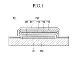
- FIG. 1 is a cross-sectional view of an organic light emitting diode (OLED) display according to a first exemplary embodiment of the present invention
- FIG. 2 is an enlarged cross-sectional view of the OLED display of FIG. 1 ;
- FIG. 3 is a cross-sectional view of an OLED display according to a second exemplary embodiment of the present invention.
- FIG. 4 is a cross-sectional view of an OLED display according to a third exemplary embodiment of the present invention.
- FIG. 5 is a cross-sectional view of an OLED display according to a fourth exemplary embodiment of the present invention.
- FIG. 6 is a comparison table of an experiment example according to the first exemplary embodiment of the present invention and three comparative examples.
- the same reference numerals are used for elements having the same configuration, and will be representatively described in a first exemplary embodiment whereas, in other exemplary embodiments, only elements different from those of the first exemplary embodiment will be described.
- Exemplary embodiments of the present invention represent ideal exemplary embodiments of the present invention in detail. As a result, modifications of diagrams are expected. Accordingly, exemplary embodiments are not limited to specific shapes of shown regions, and for example, also include modifications of the shape by manufacturing.
- OLED organic light emitting diode
- FIG. 1 is a cross-sectional view of an organic light emitting diode (OLED) display according to a first exemplary embodiment of the present invention.
- OLED organic light emitting diode
- the OLED display 101 includes a substrate 110, an organic light emitting diode 70, and a thin film encapsulation 201.
- the substrate 110 may be made of various materials known to a person skilled in the art, and the material may include glass, quartz, ceramic, and the like.
- the organic light emitting diode 70 is formed on the substrate 110. The organic light emitting diode 70 emits light and the OLED display 101 displays an image.
- the thin film encapsulation 201 protects the organic light emitting diode 70 by covering the same.
- the thin film encapsulation 201 has a multilayered structure.
- the thin film encapsulation 201 includes a first inorganic layer 211, intermediate layers 221, 222, and 223, and a second inorganic layer 212.
- the first inorganic layer 211 covers the organic light emitting diode 70.
- the first inorganic layer 211 is disposed most adjacent to the organic light emitting diode 70 among the layers of the thin film encapsulation 201. That is, the first inorganic layer 211 becomes the lowest layer of the thin film encapsulation 201.
- the intermediate layers 221, 222, and 223 are formed on the first inorganic layer 211.
- the intermediate layers 221, 222, and 223 cover a relatively smaller area than the first inorganic layer 211.
- the intermediate layers 221, 222, and 223 expose edges of the first inorganic layer 211.
- the second inorganic layer 212 is formed on the first inorganic layer 211 and the intermediate layers 221, 222, and 223.
- the second inorganic layer 212 covers a relatively larger area than the intermediate layers 221, 222, and 223.
- the second inorganic layer 212 contacts the first inorganic layer 211 at edges thereof.
- the thin film encapsulation 201 has a structure in which the first inorganic layer 211 and the second inorganic layer 212 are sequentially layered on the edges of the substrate 110, and thin film encapsulation substrate 212 has a structure in which the first inorganic layer 211, the intermediate layers 221, 222, and 223, and the second inorganic layer 212 are sequentially layered on the organic light emitting diode 70.
- the first inorganic layer 211 and the second inorganic layer 212 may be formed of a material including at least one of Al 2 O 3 , TiO 2 , ZrO, SiO 2 , AION, AIN, SiON, Si 3 N 4 , ZnO, and Ta 2 O 5 .
- the first inorganic layer 211 is formed through an atomic layer deposition (ALD) method.
- ALD atomic layer deposition
- the first inorganic layer 211 may be formed by growing the above-stated inorganic materials at a temperature lower than 100°C in order to prevent damage to the organic light emitting diode 70.
- the first inorganic layer 211 formed through the ALD method has high density so that permeation of moisture or oxygen can be effectively suppressed.
- the intermediate layers 221, 222, and 223 are formed of multi-layers including a metal oxide layer and an organic layer.
- FIG. 1 illustrates that the intermediate layers 221, 222, and 223 have a triple-layered structure of a metal oxide layer, an organic layer, and a metal oxide layer, but the first exemplary embodiment of the present invention is not limited thereto. That is, the intermediate layers 221, 222, and 223 may have various complex structures known to a person skilled in the art.
- the organic layer 222 is formed of a polymer-based material.
- the polymer-based material includes an acryl-based resin, an epoxy-based resin, polyamide, and polyethylene.
- the first inorganic layer 211 is formed most adjacent to the organic light emitting diode 70.
- the first inorganic layer 211, formed most adjacent to the organic light emitting diode 70 is formed through the above-stated ALD method, and accordingly, damage to the organic light emitting diode 70 during the process for forming the thin film encapsulation 201 can be minimized.
- the first inorganic layer 211 suppresses damage to the organic light emitting diode 70 due to plasma or other impact during the process for forming the intermediate layers 221, 222, and 223.
- the second inorganic layer 212 may also be formed using the ALD method, but it is not restrictive.
- the substrate 110, the first inorganic layer 211, and the second inorganic layer 212 have relatively excellent bonding force therebetween, and thus when the first inorganic layer 211 and the second inorganic layer 212 are sequentially layered on the edge of the substrate 110, permeation of moisture or oxygen along interlayer interfaces in the side surface direction can be effectively suppressed.
- the organic layer 222 of the intermediate layers 221, 222, and 223 have a relatively good planarization characteristic and can ease interlayer stress. That is, the intermediate layers 221, 222, and 223 may function to ease the interlayer stress between the first inorganic layer 211 and the second inorganic layer 212.
- the first inorganic layer 211 and the second inorganic layer 212 may be manufactured using the same mask, and the intermediate layers 221, 222, and 223 may be manufactured using the same mask. That is, the thin film encapsulation 201 can be formed using two types of masks. Therefore, compared to the general manufacturing of a thin film encapsulation having a gradual structure, more than two masks are not required, and therefore the manufacturing process can be simplified and productivity can be improved.
- the OLED display 101 according to the first exemplary embodiment of the present invention can effectively suppress permeation of moisture or oxygen along the interlayer interface in the side surface direction. Furthermore, the first inorganic layer 211 in the thin film encapsulation 201 is formed most adjacent to the organic light emitting diode 70 so that damage to the organic light emitting diode 70 can be minimized.
- the OLED display 101 according to the first exemplary embodiment of the present invention has a relatively simple structure, and therefore the number of masks required during the manufacturing process can be minimized.
- FIG. 2 is an enlarged cross-sectional view of the OLED display of FIG. 1 .
- the thin film transistor 10 includes a semiconductor layer 130, a gate electrode 155, a source electrode 176, and a drain electrode 177.
- the semiconductor layer 130 is formed of a polysilicon layer.
- the semiconductor layer 130 may be formed of an amorphous silicon layer, an oxide semiconductor, or the like.
- the gate electrode 155 is disposed on one area of the semiconductor layer 130, and a gate insulation layer 140 is disposed between the gate electrode 155 and the semiconductor layer 130.
- the gate electrode 155 may be formed various conductive materials known to a person skilled in the art.
- the gate insulation layer 140 may be formed so as to include at least one of tetra ethyl ortho silicate (TEOS), silicon nitride (SiN x ), and silicon oxide (SiO 2 ).
- TEOS tetra ethyl ortho silicate
- SiN x silicon nitride
- SiO 2 silicon oxide
- the gate insulation layer 140 may be a double layer formed by sequentially layering a silicon nitride layer having a thickness of 40nm and a tetra ethyl ortho silicate layer having a thickness of 80nm.
- the gate insulation layer 140 is not limited to the above-described structure in the first exemplary embodiment of the present invention.
- the source electrode 176 and the drain electrode 177 respectively contact the semiconductor layer 130.
- the source electrode 176 and the drain electrode 177 may be formed of various conductive materials known to a person skilled in the art.
- the source electrode 176 and the drain electrode 177 are separated from each other, and are insulated from the gate electrode 155.
- An interlayer insulation layer 160 may be disposed between the source electrode 176 and the drain electrode 177.
- the interlayer insulation layer 160 may be formed of various insulation materials known to a person skilled in the art.
- the organic light emitting diode 70 includes a pixel electrode 710 connected to the drain electrode 177 of the thin film transistor 10, an organic emission layer 720 formed on the pixel electrode 710, and a common electrode 730 formed on the organic emission layer 720.
- the organic light emitting diode 70 may further include a pixel defining layer 190 having an opening partially exposing the pixel electrode 710 and defining an emission area.
- the organic emission layer 720 may emit light in the opening of the pixel defining layer 190.
- the structures of the thin film transistor 10 and the organic light emitting diode 70 are not limited to the structure shown in FIG. 2 .
- the thin film transistor 10 and the organic light emitting diode 70 can have various structures that can be easily modified by a person skilled in the art.
- the OLED display 101 may further include a barrier layer 120 disposed between the thin film transistor 10 and the substrate 110.
- the barrier layer 120 may be disposed between the semiconductor layer 130 and the substrate 110.
- the barrier layer 120 may have a double-layered structure comprising a single layer of silicon nitride (SiN x ) and a double-layer of silicon nitride (SiN x ) and silicon oxide (SiO 2 ).
- the barrier layer 120 functions to prevent permeation of unnecessary components, such as an impure element or moisture, and makes the surface flat.
- the barrier layer 120 is not a required constituent, and it may be omitted according to the type and process condition of the substrate 110.
- the substrate 110 formed of a material such as glass, quartz, and ceramic is prepared.
- the organic light emitting diode 70 is formed on the substrate 110.
- the first inorganic layer 211 covering the organic light emitting diode 70 is formed on the substrate 110.
- the edge of the first inorganic layer 211 contacts the substrate 110.
- the first inorganic layer 211 is formed using a material including at least one of Al 2 O 3 , TiO 2 , ZrO, SiO 2 , AlON, AlN, SiON, Si 3 N 4 , ZnO, and Ta 2 O 5 through the ALD method.
- the first inorganic layer 211 can be formed by growing inorganic materials at a temperature lower than 100°C to prevent damage to the organic light emitting diode 70.
- the first inorganic layer 211 formed using the ALD method has a high density so that permeation of moisture or oxygen can be effectively suppressed.
- the intermediate layers 221, 222, and 223 are formed on the first inorganic layer 211.
- the intermediate layers 221, 222, and 223 are formed as a multiple layer including at least one of a metal oxide layer and an organic layer.
- the intermediate layers 221, 222, and 223 cover a relatively smaller area than the first inorganic layer 211. That is, the intermediate layers 221, 222, and 223 expose an edge of the first inorganic layer 211. Therefore, the intermediate layers 221, 222, and 223 are formed using a mask that is different from the first inorganic layer 211.
- the organic layer 222 of the intermediate layers 221, 222, and 223 may be formed using a low temperature deposition method.
- the low temperature deposition method may use plasma.
- the first inorganic layer 211 suppresses damage to the organic light emitting diode 70 during the process for forming the organic layer 222. That is, the first inorganic layer 211 can be formed without causing damage to the organic light emitting diode 70, and can suppress damage to the organic light emitting diode 70 during the post process.
- the second inorganic layer 212 is formed on the intermediate layers 221, 222, and 223.
- the second inorganic layer 212 covers a relatively larger area than the intermediate layers 221, 222, and 223.
- the second inorganic layer 212 contacts the first inorganic layer 211 at the edge thereof.
- the second inorganic layer 212 covers an area that is equivalent to the first inorganic layer 211, and in this case, the second inorganic layer 212 may be formed using the same mask used to form the first inorganic layer 211.
- the thin film encapsulation 201 has a structure in which the first inorganic layer 211 and the second inorganic layer 212 are layered on the edge of the substrate 110, and has a structure in which the first inorganic layer 211, the intermediate layers 221, 222, and 223, and the second inorganic layer 212 are layered on the organic light emitting diode 70.
- the substrate 110, the first inorganic layer 211, and the second inorganic layer 212 have a relatively strong bonding force, permeation of moisture or oxygen along an interlayer interface in the side surface direction on the edge of the substrate 110 can be effectively suppressed.
- the organic layer 222 of the intermediate layers 221, 222, and 223 forms a buffer between the first inorganic layer 211 and the second inorganic layer 212 so as to ease interlayer stress between the first inorganic layer 211 and the second inorganic layer 212.
- an OLED display 101 that can effectively suppress permeation of moisture or oxygen along the interlayer interface in the side surface direction can be easily manufactured using the manufacturing method of the OLED display according to the first exemplary embodiment of the present invention.
- the thin film encapsulation 201 can effectively suppress the permeation of moisture or oxygen along the interlayer interface in the side surface direction while being formed using two masks.
- the first inorganic layer 211 is first formed most adjacent to the organic light emitting diode 70, and thus damage to the organic light emitting diode 70 during the process for forming the thin film encapsulation 201 can be minimized.
- FIG. 3 is a cross-sectional view of an OLED display according to a second exemplary embodiment of the present invention.
- an OLED display 102 includes an intermediate layer 222 formed as a single layer.
- the intermediate layer may be an organic layer.
- the intermediate layer 222 is made of a polymer-based material.
- the polymer-based material includes an acryl-based resin, an epoxy-based resin, polyimide, and polyethylene.
- the intermediate layer 222 may be formed using a low temperature deposition method.
- the OLED display 102 can suppress permeation of moisture or oxygen along an interlayer interface in a side surface direction.
- a first inorganic layer 211 within the thin film encapsulation 202 is formed most adjacent to the organic light emitting diode 70, and thus damage to the organic light emitting diode 70 during a process for forming the thin film encapsulation 202 can be minimized.
- the OLED display 102 according to the second exemplary embodiment of the present invention has a relatively simple structure, and therefore the number of masks required during the manufacturing process can be minimized.
- the manufacturing method of the OLED display 102 according to the second exemplary embodiment of the present invention is the same as the manufacturing method of the first exemplary embodiment except that the intermediate layer 222 is formed as a single layer.
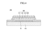
- FIG. 4 is a cross-sectional view of an OLED display according to a third exemplary embodiment of the present invention.
- an OLED display 103 according to the third exemplary embodiment of the present invention further includes an upper layer 232 formed on the second inorganic layer 212.
- the upper layer 232 covers an area relatively smaller than the second inorganic layer 212.
- the upper layer 232 can cover an area that is the same as an intermediate layer 231.
- the upper layer 232 may be formed using the mask used to form the intermediate layer 231.
- the upper layer 232 may include at least one of a metal oxide layer and an organic layer.
- the OLED display 103 can effectively suppress permeation of moisture or oxygen along the interlayer interference in the side surface direction.
- a first inorganic layer 211 within the thin film encapsulation 203 is formed most adjacent to the organic light emitting diode 70, and thus damage to the organic light emitting diode 70 during a process for forming the thin film encapsulation 203 can be minimized.
- the upper layer 232 formed on the second inorganic layer 212 protects the organic light emitting diode 70 from physical impacts.
- the manufacturing method of the OLED display 103 according to the third exemplary embodiment of the present invention is the same as the manufacturing method of the first exemplary embodiment except that a process for forming the upper layer 232 on the second inorganic layer 212 is additionally performed.
- FIG. 5 is a cross-sectional view of an OLED display according to a fourth exemplary embodiment of the present invention.
- a thin film encapsulation 204 of an OLED display 104 further includes an upper layer 242 formed on a second inorganic layer 212 and a third inorganic layer 213 formed on the upper layer 242.
- the upper layer 242 covers an area relatively smaller than the second inorganic layer 212.
- the upper layer 242 can cover an area that is the same as an intermediate layer 241.
- the upper layer 242 may be formed using a mask used to form the intermediate layer 241.
- the upper layer 242 may include at least one of a metal oxide layer and an organic layer.
- the third inorganic layer 213 is formed so as to contact the second inorganic layer 212 at an edge thereof while covering a relatively larger area than the upper layer 242.
- the third inorganic layer 213 can cover an area that is the same as the second inorganic layer 212 and, in this case, the third inorganic layer 213 may be formed using a mask used to form the first inorganic layer 211 and the second inorganic layer 212.
- the thin film encapsulation 204 has a structure in which the first inorganic layer 211, the second inorganic layer 212, and the third inorganic layer 213 are layered on an edge of the substrate 110, and has a structure in which the first inorganic layer 211, the intermediate layer 231, the second inorganic layer 212, the upper portion 242, and the third inorganic layer 213 are layered on an organic light emitting diode 70.
- the substrate 110, the first inorganic layer 211, the second inorganic layer 212, and the third inorganic layer 213 have a relatively strong bonding force, permeation of moisture or oxygen along an interlayer interface in the side surface direction on the edge of the substrate 110 can be effectively suppressed.
- the OLED display 104 that can effectively suppress permeation of moisture or oxygen along the interlayer interface in the side surface direction can be easily manufactured using the manufacturing method of the OLED display according to the first exemplary embodiment of the present invention. Furthermore, the first inorganic layer 211 within the thin film encapsulation 204 is formed most adjacent to the organic light emitting diode 70, and thus damage to the organic light emitting diode 70 during the process for forming the thin film encapsulation 204 can be minimized.
- the manufacturing method of the OLED display 104 according to the fourth exemplary embodiment of the present invention is the same as the manufacturing method of the first exemplary embodiment except that the upper layer 242 and the third inorganic layer 213 are formed on the second inorganic layer 212.
- the fourth exemplary embodiment of the present invention is not limited thereto, and the thin film encapsulation 204 may include a layered inorganic layer comprising four or more layers, an intermediate layer comprising three or more layers, and an upper layer.
- FIG. 6 is a comparison table of an experiment example according to the first exemplary embodiment of the present invention and three comparative examples.
- Comparative Example 1 includes one inorganic layer covering an organic light emitting diode, and the inorganic layer was formed using an ALD method.
- Comparative Example 2 includes an organic layer covering an organic light emitting diode, and an inorganic layer formed on the organic layer and covering an area relatively larger than the area covered by the organic layer. That is, a thin film encapsulation had a gradual structure and two or more masks were used.
- the organic layer was formed using a low temperature deposition method and the inorganic layer was formed using the ALD method.
- Comparative Example 3 includes an inorganic layer sealing an encapsulation substrate made of a known glass material and covering the encapsulation substrate.
- the inorganic layer was formed using the ALD method.
- the Experimental Example has a structure according to the first exemplary embodiment of the present invention, and materials of inorganic and organic layers were the same as those of the comparative examples.
- the Comparative Example 1 having the thin film encapsulation formed of the inorganic layer has a problem in light emission, and lighting was impossible after 408 hours.
- the experiment was performed under the 50 times of acceleration life-span condition, and therefore 72 hours of the experiment is substantially estimated to 3600 hours.
- Comparative Example 2 using the thin film encapsulation formed by forming the organic layer first and then forming the inorganic layer using the ALD method, lighting was impossible after 168 hours and thus suppression of moisture permeation was weaker than that of the Comparative Example 1.
- Comparative Example 3 the inorganic layer formed through the ALD method was added on the encapsulation substrate made of a glass material, a problem occurred in light emission after 168 hours, and lighting was impossible after 552 hours. Comparative Example 3 shows relatively strong suppression of moisture permeation compared to other comparative examples.
- the Experimental Example maintained light emission in good state even after 552 hours.
- the Experimental Example has a simple structure similar to Comparative Example 2, it has a much stronger permeation suppression force than that of Comparative Example 3, which has the most excellent permeation suppression force among the comparative examples, but a relatively complicated structure.
- the thin film encapsulation of the OLED display according to the exemplary embodiments of the present invention can minimize damage to the organic light emitting diode during a process for forming the thin film encapsulation by forming the first inorganic layer most adjacent to the organic light emitting diode first, and can effectively suppress permeation of moisture or oxygen along an interlayer interface in the side surface direction by layering inorganic layers having relatively excellent bonding force therebetween.
- the number of masks required during a process using the thin film encapsulation can be minimized, thereby improving productivity.
Abstract
Description
- The present invention relates to an organic light emitting diode (OLED) display and a manufacturing method thereof. More particularly, the present invention relates to an OLED display using thin film encapsulation, and a manufacturing method thereof.
- Unlike a liquid crystal display, the OLED display has a self-emitting characteristic and does not need a separate light source such that the thickness and weight thereof are decreased. In addition, since the OLED display involves high quality characteristics such as low power consumption, high luminance, and short response time, it is spotlighted as a next generation display device for portable electronic appliances.
- The OLED display includes a plurality of organic light emitting diodes, each having a hole injection electrode, an organic emission layer, and an electron injection electrode. Light is emitted when exciton generated by combining electrons and holes in an organic emission layer falls from an exited state to a ground state, and the OLED display displays the image using the emitted light.
- However, the organic emission layer sensitively reacts to the external environment such as moisture and oxygen. Thus, when the organic emission layer is exposed to moisture and oxygen, quality of the OLED display may deteriorate. Accordingly, in order to protect an organic light emitting diode and prevent permeation of moisture or oxygen into the organic emission layer, an encapsulation substrate may be attached in an air-tight manner to a display substrate where the organic light emitting diode is formed, or a thin film encapsulation may be formed on the organic light emitting diode.
- In particular, the entire thickness of the OLED display can be significantly reduced by using the thin film encapsulation rather than using the encapsulation substrate. Furthermore, it is advantageous to realize a flexible display.
- However, the OLED display using the thin film encapsulation can effectively prevent permeation of moisture or oxygen along a direction perpendicular to the substrate, but moisture or oxygen may be easily permeated into the substrate along an interface of the thin film encapsulation in a direction parallel to the substrate at an edge of the substrate.
- The above information disclosed in this Background section is only for enhancement of an understanding of the background of the invention, and therefore it may contain information that does not form the prior art that is already known in this country to a person of ordinary skill in the art.
- The present invention has been developed in an effort to provide an organic light emitting diode (OLED) display that can be easily manufactured by having a relatively small structure while effectively suppressing permeation of moisture and oxygen along a side surface direction.
- An OLED display according to the present invention includes: a substrate; an organic light emitting diode formed on the substrate; a first inorganic layer formed on the substrate and covering the organic light emitting diode; an intermediate layer formed on the first inorganic layer and covering an area relatively smaller than the first inorganic layer; and a second inorganic layer formed on the first inorganic layer and the intermediate layer, and contacting the first inorganic layer at an edge thereof while covering a relatively larger area than the intermediate layer.
- The first inorganic layer and the second inorganic layer may be layered on the edge of the substrate. The area of the first inorganic layer is preferably the same as the area of the second inorganic layer.
- The first inorganic layer may be formed through an atomic layer deposition (ALD) method. Preferably, the atomic layer deposition is performed at a temperature below 100°C.
- The intermediate layer may include at least one of a metal oxide layer and an organic layer.
- The OLED display may further include an upper layer formed on the second inorganic layer, and the upper layer may cover a relatively smaller area than the second inorganic layer.
- The upper layer may cover an area that is the same as the intermediate layer.
- The upper layer may include at least one of a metal oxide layer and an organic layer.
- The OLED display may include a third inorganic layer formed on the second inorganic layer and the upper layer and contacting the second inorganic layer at an edge thereof while covering a relatively larger area than the upper layer.
- The first inorganic layer, the second inorganic layer, and the third inorganic layer may be layered on the edge of the substrate. The area of the second inorganic layer is preferably the same as the area of the third inorganic layer.
- At least one of the second inorganic layer and the third inorganic layer may be formed through an ALD method. Preferably, the atomic layer deposition is performed at a temperature below 100°C.
- A manufacturing method of an OLED display according to another exemplary embodiment of the present invention includes: preparing a substrate; forming an organic light emitting diode on the substrate; forming a first inorganic layer covering the organic light emitting diode; forming an intermediate layer on the first inorganic layer and covering an area relatively smaller than the first inorganic layer; and forming a second inorganic layer on the first inorganic layer and the intermediate layer, and contacting the first inorganic layer at an edge thereof while covering a relatively larger area than the intermediate layer.
- The first inorganic layer and the second inorganic layer may be layered on an edge of the substrate. Preferably, the area of the first inorganic layer is the same as the area of the second inorganic layer and the first inorganic layer and the second inorganic layer are formed using the same mask.
- The first inorganic layer may be formed through an atomic layer deposition (ALD) method.
- The intermediate layer may include at least one of a metal oxide layer and an organic layer.
- The manufacturing method of the OLED display may further include forming an upper layer on the second inorganic layer, wherein the upper layer covers an area relatively smaller than the second inorganic layer.
- The upper layer may cover an area that is the same as the intermediate layer.
- The upper layer may include at least one of a metal oxide layer and an organic layer.
- The manufacturing method of the OLED display may further include forming a third inorganic layer on the second inorganic layer and the upper layer, and contacting the second inorganic layer at an edge thereof while covering an area relatively larger than the upper layer.
- The first inorganic layer, the second inorganic layer, and the third inorganic layer may be layered on the edge of the substrate. Preferably, the area of the second inorganic layer is preferably the same as the area of the third inorganic layer. Preferably, the first inorganic layer, the second inorganic layer and the third organic layer are formed using the same mask.
- At least one of the second inorganic layer and the third inorganic layer may be formed through the ALD method.
- According to the exemplary embodiments of the present invention, the OLED display can have a relatively simple structure while effectively suppressing permeation of moisture and oxygen along the side surface direction.
- In addition, damage to the organic light emitting diode during a process for forming the thin film encapsulation can be minimized.
- Furthermore, the OLED display can be effectively and easily manufactured.
- A more complete appreciation of the invention, and many of the attendant advantages thereof, will be readily apparent as the same becomes better understood by reference to the following detailed description when considered in conjunction with the accompanying drawings, in which like reference symbols indicate the same or similar components, wherein:
-
FIG. 1 is a cross-sectional view of an organic light emitting diode (OLED) display according to a first exemplary embodiment of the present invention; -
FIG. 2 is an enlarged cross-sectional view of the OLED display ofFIG. 1 ; -
FIG. 3 is a cross-sectional view of an OLED display according to a second exemplary embodiment of the present invention; -
FIG. 4 is a cross-sectional view of an OLED display according to a third exemplary embodiment of the present invention; -
FIG. 5 is a cross-sectional view of an OLED display according to a fourth exemplary embodiment of the present invention; and -
FIG. 6 is a comparison table of an experiment example according to the first exemplary embodiment of the present invention and three comparative examples. - The present invention will be described more fully hereinafter with reference to the accompanying drawings, in which exemplary embodiments of the invention are shown.
- As those skilled in the art will realize, the described embodiments may be modified in various different ways, all without departing from the scope of the present invention.
- In various exemplary embodiments, the same reference numerals are used for elements having the same configuration, and will be representatively described in a first exemplary embodiment whereas, in other exemplary embodiments, only elements different from those of the first exemplary embodiment will be described.
- The drawings are schematic and not proportionally scaled down. Relative scales and ratios in the drawings are enlarged or reduced for the purpose of accuracy and convenience, and the scales are random and not limited thereto. In addition, like reference numerals designate like structures, elements, or parts throughout the specification. It will be understood that, when an element is referred to as being "on" another element, it can be directly on another element or intervening elements may be present therebetween.
- Exemplary embodiments of the present invention represent ideal exemplary embodiments of the present invention in detail. As a result, modifications of diagrams are expected. Accordingly, exemplary embodiments are not limited to specific shapes of shown regions, and for example, also include modifications of the shape by manufacturing.
- Hereinafter, an organic light emitting diode (OLED) display according to a first exemplary embodiment of the present invention will be described with reference to
FIG. 1 . -
FIG. 1 is a cross-sectional view of an organic light emitting diode (OLED) display according to a first exemplary embodiment of the present invention. - As shown in
FIG. 1 , theOLED display 101 according to the first exemplary embodiment of the present invention includes asubstrate 110, an organiclight emitting diode 70, and athin film encapsulation 201. - The
substrate 110 may be made of various materials known to a person skilled in the art, and the material may include glass, quartz, ceramic, and the like. In addition, the organiclight emitting diode 70 is formed on thesubstrate 110. The organiclight emitting diode 70 emits light and theOLED display 101 displays an image. - The
thin film encapsulation 201 protects the organiclight emitting diode 70 by covering the same. In addition, thethin film encapsulation 201 has a multilayered structure. - In the first exemplary embodiment of the present invention, the
thin film encapsulation 201 includes a firstinorganic layer 211,intermediate layers inorganic layer 212. - The first
inorganic layer 211 covers the organiclight emitting diode 70. The firstinorganic layer 211 is disposed most adjacent to the organiclight emitting diode 70 among the layers of thethin film encapsulation 201. That is, the firstinorganic layer 211 becomes the lowest layer of thethin film encapsulation 201. - The
intermediate layers inorganic layer 211. Theintermediate layers inorganic layer 211. In further detail, theintermediate layers inorganic layer 211. - The second
inorganic layer 212 is formed on the firstinorganic layer 211 and theintermediate layers inorganic layer 212 covers a relatively larger area than theintermediate layers inorganic layer 212 contacts the firstinorganic layer 211 at edges thereof. - That is, the
thin film encapsulation 201 has a structure in which the firstinorganic layer 211 and the secondinorganic layer 212 are sequentially layered on the edges of thesubstrate 110, and thinfilm encapsulation substrate 212 has a structure in which the firstinorganic layer 211, theintermediate layers inorganic layer 212 are sequentially layered on the organiclight emitting diode 70. - The first
inorganic layer 211 and the secondinorganic layer 212 may be formed of a material including at least one of Al2O3, TiO2, ZrO, SiO2, AION, AIN, SiON, Si3N4, ZnO, and Ta2O5. - In addition, the first
inorganic layer 211 is formed through an atomic layer deposition (ALD) method. According to the ALD method, the firstinorganic layer 211 may be formed by growing the above-stated inorganic materials at a temperature lower than 100°C in order to prevent damage to the organiclight emitting diode 70. The firstinorganic layer 211 formed through the ALD method has high density so that permeation of moisture or oxygen can be effectively suppressed. - The
intermediate layers FIG. 1 illustrates that theintermediate layers intermediate layers - Meanwhile, the
organic layer 222 is formed of a polymer-based material. The polymer-based material includes an acryl-based resin, an epoxy-based resin, polyamide, and polyethylene. - In the first exemplary embodiment of the present invention, the first
inorganic layer 211 is formed most adjacent to the organiclight emitting diode 70. As described, the firstinorganic layer 211, formed most adjacent to the organiclight emitting diode 70, is formed through the above-stated ALD method, and accordingly, damage to the organiclight emitting diode 70 during the process for forming thethin film encapsulation 201 can be minimized. - In addition, the first
inorganic layer 211 suppresses damage to the organiclight emitting diode 70 due to plasma or other impact during the process for forming theintermediate layers - The second
inorganic layer 212 may also be formed using the ALD method, but it is not restrictive. - Furthermore, the
substrate 110, the firstinorganic layer 211, and the secondinorganic layer 212 have relatively excellent bonding force therebetween, and thus when the firstinorganic layer 211 and the secondinorganic layer 212 are sequentially layered on the edge of thesubstrate 110, permeation of moisture or oxygen along interlayer interfaces in the side surface direction can be effectively suppressed. - In addition, the
organic layer 222 of theintermediate layers intermediate layers inorganic layer 211 and the secondinorganic layer 212. - Furthermore, the first
inorganic layer 211 and the secondinorganic layer 212 may be manufactured using the same mask, and theintermediate layers thin film encapsulation 201 can be formed using two types of masks. Therefore, compared to the general manufacturing of a thin film encapsulation having a gradual structure, more than two masks are not required, and therefore the manufacturing process can be simplified and productivity can be improved. - With such a configuration, the
OLED display 101 according to the first exemplary embodiment of the present invention can effectively suppress permeation of moisture or oxygen along the interlayer interface in the side surface direction. Furthermore, the firstinorganic layer 211 in thethin film encapsulation 201 is formed most adjacent to the organiclight emitting diode 70 so that damage to the organiclight emitting diode 70 can be minimized. - In addition, the
OLED display 101 according to the first exemplary embodiment of the present invention has a relatively simple structure, and therefore the number of masks required during the manufacturing process can be minimized. - Hereinafter, structures of the organic
light emitting diode 70 and a thin film transistor for driving the organiclight emitting diode 70 formed on thesubstrate 110 in theOLED display 101 will now be described in further detail with reference toFIG. 2 . -
FIG. 2 is an enlarged cross-sectional view of the OLED display ofFIG. 1 . - The
thin film transistor 10 includes asemiconductor layer 130, agate electrode 155, asource electrode 176, and adrain electrode 177. - In the first exemplary embodiment of the present invention, the
semiconductor layer 130 is formed of a polysilicon layer. However, the first exemplary embodiment of the present invention is not limited thereto. Thus, thesemiconductor layer 130 may be formed of an amorphous silicon layer, an oxide semiconductor, or the like. - The
gate electrode 155 is disposed on one area of thesemiconductor layer 130, and agate insulation layer 140 is disposed between thegate electrode 155 and thesemiconductor layer 130. Thegate electrode 155 may be formed various conductive materials known to a person skilled in the art. Thegate insulation layer 140 may be formed so as to include at least one of tetra ethyl ortho silicate (TEOS), silicon nitride (SiNx), and silicon oxide (SiO2). For example, thegate insulation layer 140 may be a double layer formed by sequentially layering a silicon nitride layer having a thickness of 40nm and a tetra ethyl ortho silicate layer having a thickness of 80nm. However, thegate insulation layer 140 is not limited to the above-described structure in the first exemplary embodiment of the present invention. - The
source electrode 176 and thedrain electrode 177 respectively contact thesemiconductor layer 130. Thesource electrode 176 and thedrain electrode 177 may be formed of various conductive materials known to a person skilled in the art. Thesource electrode 176 and thedrain electrode 177 are separated from each other, and are insulated from thegate electrode 155. Aninterlayer insulation layer 160 may be disposed between thesource electrode 176 and thedrain electrode 177. Theinterlayer insulation layer 160 may be formed of various insulation materials known to a person skilled in the art. - The organic
light emitting diode 70 includes apixel electrode 710 connected to thedrain electrode 177 of thethin film transistor 10, anorganic emission layer 720 formed on thepixel electrode 710, and acommon electrode 730 formed on theorganic emission layer 720. In addition, the organiclight emitting diode 70 may further include apixel defining layer 190 having an opening partially exposing thepixel electrode 710 and defining an emission area. Theorganic emission layer 720 may emit light in the opening of thepixel defining layer 190. - In addition, in the first exemplary embodiment of the present invention, the structures of the
thin film transistor 10 and the organiclight emitting diode 70 are not limited to the structure shown inFIG. 2 . Thethin film transistor 10 and the organiclight emitting diode 70 can have various structures that can be easily modified by a person skilled in the art. - The
OLED display 101 may further include abarrier layer 120 disposed between thethin film transistor 10 and thesubstrate 110. In further detail, thebarrier layer 120 may be disposed between thesemiconductor layer 130 and thesubstrate 110. For example, thebarrier layer 120 may have a double-layered structure comprising a single layer of silicon nitride (SiNx) and a double-layer of silicon nitride (SiNx) and silicon oxide (SiO2). Thebarrier layer 120 functions to prevent permeation of unnecessary components, such as an impure element or moisture, and makes the surface flat. However, thebarrier layer 120 is not a required constituent, and it may be omitted according to the type and process condition of thesubstrate 110. - Hereinafter, a manufacturing method of the
OLED display 101 according to the first exemplary embodiment of the present invention will be described. - First, the
substrate 110 formed of a material such as glass, quartz, and ceramic is prepared. In addition, the organiclight emitting diode 70 is formed on thesubstrate 110. - Next, the first
inorganic layer 211 covering the organiclight emitting diode 70 is formed on thesubstrate 110. In this case, the edge of the firstinorganic layer 211 contacts thesubstrate 110. In addition, the firstinorganic layer 211 is formed using a material including at least one of Al2O3, TiO2, ZrO, SiO2, AlON, AlN, SiON, Si3N4, ZnO, and Ta2O5 through the ALD method. According to the ALD method, the firstinorganic layer 211 can be formed by growing inorganic materials at a temperature lower than 100°C to prevent damage to the organiclight emitting diode 70. Furthermore, the firstinorganic layer 211 formed using the ALD method has a high density so that permeation of moisture or oxygen can be effectively suppressed. - Next, the
intermediate layers inorganic layer 211. In the first exemplary embodiment of the present invention, theintermediate layers - In addition, the
intermediate layers inorganic layer 211. That is, theintermediate layers inorganic layer 211. Therefore, theintermediate layers inorganic layer 211. - The
organic layer 222 of theintermediate layers inorganic layer 211 suppresses damage to the organiclight emitting diode 70 during the process for forming theorganic layer 222. That is, the firstinorganic layer 211 can be formed without causing damage to the organiclight emitting diode 70, and can suppress damage to the organiclight emitting diode 70 during the post process. - Next, the second
inorganic layer 212 is formed on theintermediate layers inorganic layer 212 covers a relatively larger area than theintermediate layers inorganic layer 212 contacts the firstinorganic layer 211 at the edge thereof. The secondinorganic layer 212 covers an area that is equivalent to the firstinorganic layer 211, and in this case, the secondinorganic layer 212 may be formed using the same mask used to form the firstinorganic layer 211. - As described, the
thin film encapsulation 201 has a structure in which the firstinorganic layer 211 and the secondinorganic layer 212 are layered on the edge of thesubstrate 110, and has a structure in which the firstinorganic layer 211, theintermediate layers inorganic layer 212 are layered on the organiclight emitting diode 70. - Furthermore, since the
substrate 110, the firstinorganic layer 211, and the secondinorganic layer 212 have a relatively strong bonding force, permeation of moisture or oxygen along an interlayer interface in the side surface direction on the edge of thesubstrate 110 can be effectively suppressed. - Meanwhile, the
organic layer 222 of theintermediate layers inorganic layer 211 and the secondinorganic layer 212 so as to ease interlayer stress between the firstinorganic layer 211 and the secondinorganic layer 212. - With such a manufacturing method, an
OLED display 101 that can effectively suppress permeation of moisture or oxygen along the interlayer interface in the side surface direction can be easily manufactured using the manufacturing method of the OLED display according to the first exemplary embodiment of the present invention. - In further detail, according to the first exemplary embodiment of the present invention, the
thin film encapsulation 201 can effectively suppress the permeation of moisture or oxygen along the interlayer interface in the side surface direction while being formed using two masks. - In addition, according to the first exemplary embodiment of the present invention, the first
inorganic layer 211 is first formed most adjacent to the organiclight emitting diode 70, and thus damage to the organiclight emitting diode 70 during the process for forming thethin film encapsulation 201 can be minimized. - Hereinafter, an OLED display according to a second exemplary embodiment of the present invention will be described with reference to
FIG. 3 . -
FIG. 3 is a cross-sectional view of an OLED display according to a second exemplary embodiment of the present invention. - As shown in
FIG. 3 , anOLED display 102 according to the second exemplary embodiment of the present invention includes anintermediate layer 222 formed as a single layer. In this case, the intermediate layer may be an organic layer. Thus, theintermediate layer 222 is made of a polymer-based material. In this regard, the polymer-based material includes an acryl-based resin, an epoxy-based resin, polyimide, and polyethylene. In addition, theintermediate layer 222 may be formed using a low temperature deposition method. - With such a configuration, the
OLED display 102 according to the second exemplary embodiment of the present invention can suppress permeation of moisture or oxygen along an interlayer interface in a side surface direction. In addition, a firstinorganic layer 211 within thethin film encapsulation 202 is formed most adjacent to the organiclight emitting diode 70, and thus damage to the organiclight emitting diode 70 during a process for forming thethin film encapsulation 202 can be minimized. - Furthermore, the
OLED display 102 according to the second exemplary embodiment of the present invention has a relatively simple structure, and therefore the number of masks required during the manufacturing process can be minimized. - The manufacturing method of the
OLED display 102 according to the second exemplary embodiment of the present invention is the same as the manufacturing method of the first exemplary embodiment except that theintermediate layer 222 is formed as a single layer. - Hereinafter, an OLED display according to a third exemplary embodiment of the present invention will be described with reference to
FIG. 4 . -
FIG. 4 is a cross-sectional view of an OLED display according to a third exemplary embodiment of the present invention. - As shown in
FIG. 4 , anOLED display 103 according to the third exemplary embodiment of the present invention further includes anupper layer 232 formed on the secondinorganic layer 212. Theupper layer 232 covers an area relatively smaller than the secondinorganic layer 212. In further detail, theupper layer 232 can cover an area that is the same as anintermediate layer 231. In this case, theupper layer 232 may be formed using the mask used to form theintermediate layer 231. In addition, like theintermediate layer 231, theupper layer 232 may include at least one of a metal oxide layer and an organic layer. - With such a configuration, the
OLED display 103 according to the third exemplary embodiment of the present invention can effectively suppress permeation of moisture or oxygen along the interlayer interference in the side surface direction. In addition, a firstinorganic layer 211 within thethin film encapsulation 203 is formed most adjacent to the organiclight emitting diode 70, and thus damage to the organiclight emitting diode 70 during a process for forming thethin film encapsulation 203 can be minimized. Moreover, theupper layer 232 formed on the secondinorganic layer 212 protects the organiclight emitting diode 70 from physical impacts. - The manufacturing method of the
OLED display 103 according to the third exemplary embodiment of the present invention is the same as the manufacturing method of the first exemplary embodiment except that a process for forming theupper layer 232 on the secondinorganic layer 212 is additionally performed. - Hereinafter, an OLED display according to a fourth exemplary embodiment of the present invention will be described with reference to
FIG. 5 -
FIG. 5 is a cross-sectional view of an OLED display according to a fourth exemplary embodiment of the present invention. - As shown in
FIG. 5 , athin film encapsulation 204 of anOLED display 104 according to the fourth exemplary embodiment of the present invention further includes anupper layer 242 formed on a secondinorganic layer 212 and a thirdinorganic layer 213 formed on theupper layer 242. - The
upper layer 242 covers an area relatively smaller than the secondinorganic layer 212. In further detail, theupper layer 242 can cover an area that is the same as anintermediate layer 241. In this case, theupper layer 242 may be formed using a mask used to form theintermediate layer 241. Furthermore, like theintermediate layer 241, theupper layer 242 may include at least one of a metal oxide layer and an organic layer. - The third
inorganic layer 213 is formed so as to contact the secondinorganic layer 212 at an edge thereof while covering a relatively larger area than theupper layer 242. In further detail, the thirdinorganic layer 213 can cover an area that is the same as the secondinorganic layer 212 and, in this case, the thirdinorganic layer 213 may be formed using a mask used to form the firstinorganic layer 211 and the secondinorganic layer 212. - As described, the
thin film encapsulation 204 has a structure in which the firstinorganic layer 211, the secondinorganic layer 212, and the thirdinorganic layer 213 are layered on an edge of thesubstrate 110, and has a structure in which the firstinorganic layer 211, theintermediate layer 231, the secondinorganic layer 212, theupper portion 242, and the thirdinorganic layer 213 are layered on an organiclight emitting diode 70. - In addition, since the
substrate 110, the firstinorganic layer 211, the secondinorganic layer 212, and the thirdinorganic layer 213 have a relatively strong bonding force, permeation of moisture or oxygen along an interlayer interface in the side surface direction on the edge of thesubstrate 110 can be effectively suppressed. - With such a manufacturing method, the
OLED display 104 that can effectively suppress permeation of moisture or oxygen along the interlayer interface in the side surface direction can be easily manufactured using the manufacturing method of the OLED display according to the first exemplary embodiment of the present invention. Furthermore, the firstinorganic layer 211 within thethin film encapsulation 204 is formed most adjacent to the organiclight emitting diode 70, and thus damage to the organiclight emitting diode 70 during the process for forming thethin film encapsulation 204 can be minimized. - The manufacturing method of the
OLED display 104 according to the fourth exemplary embodiment of the present invention is the same as the manufacturing method of the first exemplary embodiment except that theupper layer 242 and the thirdinorganic layer 213 are formed on the secondinorganic layer 212. - However, the fourth exemplary embodiment of the present invention is not limited thereto, and the
thin film encapsulation 204 may include a layered inorganic layer comprising four or more layers, an intermediate layer comprising three or more layers, and an upper layer. - Hereinafter, experiment examples and different comparative examples according to the first exemplary embodiment of the present invention will be described with reference to
FIG. 6 . -
FIG. 6 is a comparison table of an experiment example according to the first exemplary embodiment of the present invention and three comparative examples. - The life-span evaluation experiments were performed with the experimental example and the comparative examples, and the experiment was performed under 50 times of acceleration life-span condition.
- Comparative Example 1 includes one inorganic layer covering an organic light emitting diode, and the inorganic layer was formed using an ALD method.
- Comparative Example 2 includes an organic layer covering an organic light emitting diode, and an inorganic layer formed on the organic layer and covering an area relatively larger than the area covered by the organic layer. That is, a thin film encapsulation had a gradual structure and two or more masks were used. The organic layer was formed using a low temperature deposition method and the inorganic layer was formed using the ALD method.
- Comparative Example 3 includes an inorganic layer sealing an encapsulation substrate made of a known glass material and covering the encapsulation substrate. The inorganic layer was formed using the ALD method.
- The Experimental Example has a structure according to the first exemplary embodiment of the present invention, and materials of inorganic and organic layers were the same as those of the comparative examples.
- As shown in
FIG. 6 , although the ALD method was used, the Comparative Example 1 having the thin film encapsulation formed of the inorganic layer has a problem in light emission, and lighting was impossible after 408 hours. In this regard, the experiment was performed under the 50 times of acceleration life-span condition, and therefore 72 hours of the experiment is substantially estimated to 3600 hours. - According to Comparative Example 2, using the thin film encapsulation formed by forming the organic layer first and then forming the inorganic layer using the ALD method, lighting was impossible after 168 hours and thus suppression of moisture permeation was weaker than that of the Comparative Example 1.
- According to Comparative Example 3, the inorganic layer formed through the ALD method was added on the encapsulation substrate made of a glass material, a problem occurred in light emission after 168 hours, and lighting was impossible after 552 hours. Comparative Example 3 shows relatively strong suppression of moisture permeation compared to other comparative examples.
- Meanwhile, the Experimental Example maintained light emission in good state even after 552 hours. Thus, while the Experimental Example has a simple structure similar to Comparative Example 2, it has a much stronger permeation suppression force than that of Comparative Example 3, which has the most excellent permeation suppression force among the comparative examples, but a relatively complicated structure.
- As shown in the above-described experiments, the thin film encapsulation of the OLED display according to the exemplary embodiments of the present invention can minimize damage to the organic light emitting diode during a process for forming the thin film encapsulation by forming the first inorganic layer most adjacent to the organic light emitting diode first, and can effectively suppress permeation of moisture or oxygen along an interlayer interface in the side surface direction by layering inorganic layers having relatively excellent bonding force therebetween.
- Furthermore, the number of masks required during a process using the thin film encapsulation can be minimized, thereby improving productivity.
- While this invention has been described in connection with what is presently considered to be practical exemplary embodiments, it is to be understood that the invention is not limited to the disclosed embodiments but, on the contrary, is intended to cover various modifications and equivalent arrangements included within the scope of the appended claims.
Claims (15)
- An organic light emitting diode (OLED) display (101, 102, 103, 104), comprising:a substrate (110);an organic light emitting diode (70) formed on the substrate (110);a first inorganic layer (211) formed on the substrate (110) and completely covering the organic light emitting diode (70);an intermediate layer (221, 222, 223, 231, 241) formed on the first inorganic (211) layer and covering an area smaller than an area of the first inorganic layer (211); anda second inorganic layer (212) formed on the first inorganic layer (211) and the intermediate layer (221, 222, 223, 231, 241) and contacting the first inorganic layer (211) at an edge thereof while covering an area larger than the area of the intermediate layer (221, 222, 223, 231, 241).
- The OLED display of claim 1, wherein the area of the first inorganic layer (211) is the same as the area of the second inorganic layer (212).
- The OLED display of one of the preceding claims, wherein the intermediate layer (221, 222, 223, 231, 241) comprises at least one of a metal oxide layer and an organic layer.
- The OLED display of one of the preceding claims, further comprising an upper layer (232, 242) formed on the second inorganic layer (212), wherein the upper layer (232, 242) covers an area smaller than the area of the second inorganic layer (212).
- The OLED display of claim 4, wherein the upper layer (232, 242) covers an area that is the same as the area of the intermediate layer (231, 241).
- The OLED display of one of claims 4 and 5, wherein the upper layer (232, 242) comprises at least one of a metal oxide layer and an organic layer.
- The OLED display of one of claims 4 to 6, further comprising a third inorganic layer (213) formed on the second inorganic layer (212) and the upper layer (242) and contacting the second inorganic layer (212) at an edge thereof while covering an area larger than the area of the upper layer (242).
- The OLED display of claim 7, wherein the area of the second inorganic layer (212) is the same as the area of the third inorganic layer (213).
- A manufacturing method of an organic light emitting diode (OLED) display (101, 102, 103, 104) according to one of the preceding claims, comprising the steps of:preparing a substrate (110);forming an organic light emitting diode (70) on the substrate (110);forming a first inorganic layer (211) completely covering the organic light emitting diode (70);forming an intermediate layer (221, 222, 223, 231, 241) on the first inorganic layer (211) and covering an area smaller than an area of the first inorganic layer (211); andforming a second inorganic layer (212) on the first inorganic layer (211) and the intermediate layer (221, 222, 223, 231, 241) and contacting the first inorganic layer (211) at an edge thereof while covering an area larger than the area of the intermediate layer (221, 222, 223, 231, 241).
- The manufacturing method of the OLED display of claim 9, wherein the first inorganic layer (211) and the second inorganic layer (212) are formed using the same mask.
- The manufacturing method of the OLED display of one of claims 9 and 10, wherein the first inorganic layer (211) is formed by an atomic layer deposition (ALD) method.
- The manufacturing method of the OLED display of claim 11, wherein the atomic layer deposition is performed at a temperature below 100°C.
- The manufacturing method of the OLED display of one of claims 9 to 12, further comprising the step of forming an upper layer (232, 242) on the second inorganic layer (212), wherein the upper layer (232, 242) covers an area smaller than the area of the second inorganic layer (212).
- The manufacturing method of the OLED display of claim 13, further comprising the step of forming a third inorganic layer (213) on the second inorganic layer (212) and the upper layer (242), and contacting the second inorganic layer (212) at an edge thereof while covering an area larger than the area of the upper layer (242).
- The manufacturing method of the OLED display of claim 14, wherein at least one of the second inorganic layer (212) and the third inorganic layer (213) is formed by an atomic layer deposition (ALD) method.
Applications Claiming Priority (1)
| Application Number | Priority Date | Filing Date | Title |
|---|---|---|---|
| KR1020110105429A KR101809659B1 (en) | 2011-10-14 | 2011-10-14 | Organic light emitting diode display and method for manufacturing the same |
Publications (2)
| Publication Number | Publication Date |
|---|---|
| EP2581958A2 true EP2581958A2 (en) | 2013-04-17 |
| EP2581958A3 EP2581958A3 (en) | 2015-07-15 |
Family
ID=47080310
Family Applications (1)
| Application Number | Title | Priority Date | Filing Date |
|---|---|---|---|
| EP12188295.5A Ceased EP2581958A3 (en) | 2011-10-14 | 2012-10-12 | Organic light emitting diode display and method for manufacturing the same |
Country Status (3)
| Country | Link |
|---|---|
| US (1) | US8975660B2 (en) |
| EP (1) | EP2581958A3 (en) |
| KR (1) | KR101809659B1 (en) |
Cited By (4)
| Publication number | Priority date | Publication date | Assignee | Title |
|---|---|---|---|---|
| US20160095172A1 (en) * | 2014-09-30 | 2016-03-31 | Lg Display Co., Ltd. | Flexible organic light emitting display device |
| EP3016167A1 (en) * | 2014-10-31 | 2016-05-04 | LG Display Co., Ltd. | Organic light-emitting display device |
| CN107425132A (en) * | 2013-12-03 | 2017-12-01 | 乐金显示有限公司 | Organic light emitting apparatus |
| CN107534095A (en) * | 2015-05-14 | 2018-01-02 | 应用材料公司 | Encapsulation membrane stack for OLED applications |
Families Citing this family (27)
| Publication number | Priority date | Publication date | Assignee | Title |
|---|---|---|---|---|
| KR101970361B1 (en) * | 2012-08-20 | 2019-04-19 | 삼성디스플레이 주식회사 | Organic light emitting diode device and manufacturing method thereof |
| US10355242B2 (en) * | 2013-04-25 | 2019-07-16 | Sharp Kabushiki Kaisha | Electroluminescent device including a plurality of sealing films |
| KR102054850B1 (en) * | 2013-05-30 | 2019-12-12 | 삼성디스플레이 주식회사 | Organic light emitting display apparatus and method of manufacturing the same |
| KR102047006B1 (en) * | 2013-06-07 | 2019-12-03 | 삼성디스플레이 주식회사 | Organic luminescence emitting display device |
| KR102129035B1 (en) * | 2013-08-01 | 2020-07-02 | 삼성디스플레이 주식회사 | Organic light emitting display apparatus and the manufacturing method thereof |
| KR102109743B1 (en) * | 2013-12-09 | 2020-05-12 | 엘지디스플레이 주식회사 | Organic Light Emitting Display Apparatus and Method for Manufacturing The Same |
| KR102102913B1 (en) * | 2013-12-31 | 2020-04-21 | 엘지디스플레이 주식회사 | Method for Manufacturing Organic Emitting Display Device and Display Device Applying the Same |
| JP6374188B2 (en) * | 2014-03-14 | 2018-08-15 | 東京エレクトロン株式会社 | Method for forming sealing structure, manufacturing apparatus for sealing structure, manufacturing method for organic EL element structure, and manufacturing apparatus therefor |
| KR102306003B1 (en) * | 2014-04-22 | 2021-09-28 | 삼성디스플레이 주식회사 | Organic light emitting diode display and method for manufacturing organic light emitting diode display using the same |
| FR3023654B1 (en) * | 2014-07-09 | 2016-08-26 | Commissariat Energie Atomique | ENCAPSULATION OF AN ORGANIC OPTOELECTRONIC COMPONENT |
| KR102322012B1 (en) * | 2014-10-20 | 2021-11-05 | 삼성디스플레이 주식회사 | Apparatus and method for manufacturing display apparatus |
| WO2016084256A1 (en) * | 2014-11-28 | 2016-06-02 | パイオニア株式会社 | Light emitting device |
| KR101877402B1 (en) | 2015-02-24 | 2018-07-13 | 에이피시스템 주식회사 | Passivation film for organic electronic devices and Method for depositing the same |
| KR102424597B1 (en) * | 2015-06-30 | 2022-07-25 | 엘지디스플레이 주식회사 | flexible organic light emitting diode display device and method of fabricating the same |
| KR102486876B1 (en) | 2015-07-07 | 2023-01-11 | 삼성디스플레이 주식회사 | Organic light-emitting display apparatus and manufacturing the same |
| KR102322083B1 (en) | 2015-07-28 | 2021-11-04 | 삼성디스플레이 주식회사 | Organic light emitting diode display and manufacturing method thereof |
| KR102366421B1 (en) * | 2015-07-29 | 2022-02-23 | 엘지디스플레이 주식회사 | Backplate for foldable display device and foldable display device including the same |
| KR20180028850A (en) | 2016-09-09 | 2018-03-19 | 엘지디스플레이 주식회사 | Organic light emitting display device |
| KR20180064600A (en) * | 2016-12-05 | 2018-06-15 | 삼성디스플레이 주식회사 | Flexible organic light emitting display apparatus and the manufacturing method thereof |
| US10991910B2 (en) * | 2017-03-30 | 2021-04-27 | Sharp Kabushiki Kaisha | Display device and production method therefor |
| CN107104199A (en) | 2017-04-19 | 2017-08-29 | 武汉华星光电技术有限公司 | Display panel and its manufacture method |
| US10741792B2 (en) * | 2018-05-21 | 2020-08-11 | Wuhan China Star Optoelectronics Semiconductor Display Technology Co., Ltd. | Inorganic material having alkoxy chain encapsulating a display panel |
| KR102075841B1 (en) * | 2018-08-29 | 2020-02-10 | 고려대학교 세종산학협력단 | Flexible Display and Manufacturing Method thereof |
| JP2021034261A (en) * | 2019-08-27 | 2021-03-01 | 株式会社ジャパンディスプレイ | Display device |
| KR20210079898A (en) * | 2019-12-20 | 2021-06-30 | 엘지디스플레이 주식회사 | Display device |
| DE102020200053A1 (en) * | 2020-01-06 | 2021-07-08 | Heliatek Gmbh | Encapsulation system for an optoelectronic component with at least one first encapsulation and one second encapsulation, optoelectronic component with such an encapsulation system |
| CN111668271B (en) * | 2020-06-11 | 2021-08-24 | 武汉华星光电半导体显示技术有限公司 | OLED display panel, preparation method thereof and OLED display device |
Family Cites Families (10)
| Publication number | Priority date | Publication date | Assignee | Title |
|---|---|---|---|---|
| US7109653B2 (en) | 2002-01-15 | 2006-09-19 | Seiko Epson Corporation | Sealing structure with barrier membrane for electronic element, display device, electronic apparatus, and fabrication method for electronic element |
| US8900366B2 (en) * | 2002-04-15 | 2014-12-02 | Samsung Display Co., Ltd. | Apparatus for depositing a multilayer coating on discrete sheets |
| US20050212419A1 (en) * | 2004-03-23 | 2005-09-29 | Eastman Kodak Company | Encapsulating oled devices |
| KR101292297B1 (en) | 2006-09-13 | 2013-08-01 | 주성엔지니어링(주) | Organic electroluminescent element and method of manufacturing the same |
| US7560747B2 (en) * | 2007-05-01 | 2009-07-14 | Eastman Kodak Company | Light-emitting device having improved light output |
| KR100873704B1 (en) | 2007-06-13 | 2008-12-12 | 삼성모바일디스플레이주식회사 | Organic light emitting display device and fabrication method for the same |
| JP4670875B2 (en) * | 2008-02-13 | 2011-04-13 | セイコーエプソン株式会社 | Organic EL device |
| KR101001552B1 (en) | 2009-01-20 | 2010-12-17 | 삼성모바일디스플레이주식회사 | Organic light emitting display apparatus |
| KR20100097513A (en) | 2009-02-26 | 2010-09-03 | 삼성모바일디스플레이주식회사 | Organic light emitting diode display |
| KR101089715B1 (en) | 2009-11-05 | 2011-12-07 | 한국기계연구원 | Multi layer thin film for encapsulation and the method thereof |
-
2011
- 2011-10-14 KR KR1020110105429A patent/KR101809659B1/en active IP Right Grant
-
2012
- 2012-04-03 US US13/438,574 patent/US8975660B2/en active Active
- 2012-10-12 EP EP12188295.5A patent/EP2581958A3/en not_active Ceased
Non-Patent Citations (1)
| Title |
|---|
| None |
Cited By (9)
| Publication number | Priority date | Publication date | Assignee | Title |
|---|---|---|---|---|
| CN107425132A (en) * | 2013-12-03 | 2017-12-01 | 乐金显示有限公司 | Organic light emitting apparatus |
| US20160095172A1 (en) * | 2014-09-30 | 2016-03-31 | Lg Display Co., Ltd. | Flexible organic light emitting display device |
| CN105470407A (en) * | 2014-09-30 | 2016-04-06 | 乐金显示有限公司 | Flexible organic light emitting display device |
| EP3002799A1 (en) * | 2014-09-30 | 2016-04-06 | LG Display Co., Ltd. | Flexible organic light emitting display device |
| US10021741B2 (en) * | 2014-09-30 | 2018-07-10 | Lg Display Co., Ltd. | Flexible organic light emitting display device |
| EP3016167A1 (en) * | 2014-10-31 | 2016-05-04 | LG Display Co., Ltd. | Organic light-emitting display device |
| CN105609524A (en) * | 2014-10-31 | 2016-05-25 | 乐金显示有限公司 | Organic light-emitting display device |
| US9773994B2 (en) | 2014-10-31 | 2017-09-26 | Lg Display Co., Ltd. | Organic light-emitting diode display for suppressing organic light-emitting element from being damaged |
| CN107534095A (en) * | 2015-05-14 | 2018-01-02 | 应用材料公司 | Encapsulation membrane stack for OLED applications |
Also Published As
| Publication number | Publication date |
|---|---|
| KR20130040574A (en) | 2013-04-24 |
| US20130092972A1 (en) | 2013-04-18 |
| US8975660B2 (en) | 2015-03-10 |
| KR101809659B1 (en) | 2017-12-18 |
| EP2581958A3 (en) | 2015-07-15 |
Similar Documents
| Publication | Publication Date | Title |
|---|---|---|
| US8975660B2 (en) | Organic light emitting diode display and method for manufacturing the same | |
| US11793028B2 (en) | Organic light emitting diode display and method for manufacturing the same | |
| US10593906B2 (en) | Organic light-emitting display apparatus and method of manufacturing the same | |
| JP7203763B2 (en) | DISPLAY SUBSTRATE AND MANUFACTURING METHOD THEREOF, DISPLAY DEVICE | |
| CN104103665B (en) | Oganic light-emitting display device and the method for manufacturing it | |
| US9252388B2 (en) | Organic light emitting diode (OLED) display | |
| TWI641127B (en) | Organic light-emitting display apparatus and method of manufacturing the same | |
| US10944071B2 (en) | Organic light-emitting display apparatus and method of manufacturing the same | |
| EP2863447B1 (en) | Organic light emitting device and method of fabricating the same | |
| US9040961B2 (en) | Organic light emitting diode display and method for manufacturing the same | |
| KR102201296B1 (en) | flexible organic light emitting diode display device and method of fabricating the same | |
| CN106328671A (en) | Flexible organic light emitting diode display device and method of fabricating the same | |
| KR101903056B1 (en) | Organic light emitting display apparatus and the method for manufacturing the same | |
| TW201138094A (en) | Organic light emitting display device and method of manufacturing the same | |
| US20150263312A1 (en) | Thin film transistor element substrate, method of producing the substrate, and organic el display device including the thin film transistor element substrate | |
| TW201637257A (en) | Transparent organic light emitting display apparatus | |
| KR20180035954A (en) | Thin film transistor array panel and manufacturing method thereof | |
| WO2018113005A1 (en) | Oled packaging method and oled packaging structure | |
| KR101990131B1 (en) | Organic light emitting diode display and method for manufacturing the same | |
| KR101940231B1 (en) | Organic light emitting diode display and method for manufacturing the same | |
| KR102209241B1 (en) | Organic light emitting display apparatus and manufacturing the same | |
| JP5105739B2 (en) | Organic EL display device and manufacturing method thereof | |
| JP4854279B2 (en) | Organic EL display device and manufacturing method thereof | |
| JP2011142365A (en) | Organic el display device and method of manufacturing the same |
Legal Events
| Date | Code | Title | Description |
|---|---|---|---|
| PUAI | Public reference made under article 153(3) epc to a published international application that has entered the european phase |
Free format text: ORIGINAL CODE: 0009012 |
|
| AK | Designated contracting states |
Kind code of ref document: A2 Designated state(s): AL AT BE BG CH CY CZ DE DK EE ES FI FR GB GR HR HU IE IS IT LI LT LU LV MC MK MT NL NO PL PT RO RS SE SI SK SM TR |
|
| AX | Request for extension of the european patent |
Extension state: BA ME |
|
| PUAL | Search report despatched |
Free format text: ORIGINAL CODE: 0009013 |
|
| AK | Designated contracting states |
Kind code of ref document: A3 Designated state(s): AL AT BE BG CH CY CZ DE DK EE ES FI FR GB GR HR HU IE IS IT LI LT LU LV MC MK MT NL NO PL PT RO RS SE SI SK SM TR |
|
| AX | Request for extension of the european patent |
Extension state: BA ME |
|
| RIC1 | Information provided on ipc code assigned before grant |
Ipc: H01L 27/32 20060101ALI20150605BHEP Ipc: H01L 51/52 20060101AFI20150605BHEP |
|
| RAP1 | Party data changed (applicant data changed or rights of an application transferred) |
Owner name: SAMSUNG DISPLAY CO., LTD. |
|
| 17P | Request for examination filed |
Effective date: 20160114 |
|
| RBV | Designated contracting states (corrected) |
Designated state(s): AL AT BE BG CH CY CZ DE DK EE ES FI FR GB GR HR HU IE IS IT LI LT LU LV MC MK MT NL NO PL PT RO RS SE SI SK SM TR |
|
| 17Q | First examination report despatched |
Effective date: 20170123 |
|
| STAA | Information on the status of an ep patent application or granted ep patent |
Free format text: STATUS: THE APPLICATION HAS BEEN REFUSED |
|
| 18R | Application refused |
Effective date: 20180326 |