EP2579332A1 - Solar cell module and solar cell module manufacturing method - Google Patents
Solar cell module and solar cell module manufacturing method Download PDFInfo
- Publication number
- EP2579332A1 EP2579332A1 EP11789722.3A EP11789722A EP2579332A1 EP 2579332 A1 EP2579332 A1 EP 2579332A1 EP 11789722 A EP11789722 A EP 11789722A EP 2579332 A1 EP2579332 A1 EP 2579332A1
- Authority
- EP
- European Patent Office
- Prior art keywords
- solar cell
- electrode
- tab
- tabs
- cell module
- Prior art date
- Legal status (The legal status is an assumption and is not a legal conclusion. Google has not performed a legal analysis and makes no representation as to the accuracy of the status listed.)
- Granted
Links
Images






Classifications
-
- H—ELECTRICITY
- H10—SEMICONDUCTOR DEVICES; ELECTRIC SOLID-STATE DEVICES NOT OTHERWISE PROVIDED FOR
- H10F—INORGANIC SEMICONDUCTOR DEVICES SENSITIVE TO INFRARED RADIATION, LIGHT, ELECTROMAGNETIC RADIATION OF SHORTER WAVELENGTH OR CORPUSCULAR RADIATION
- H10F19/00—Integrated devices, or assemblies of multiple devices, comprising at least one photovoltaic cell covered by group H10F10/00, e.g. photovoltaic modules
- H10F19/90—Structures for connecting between photovoltaic cells, e.g. interconnections or insulating spacers
-
- H—ELECTRICITY
- H10—SEMICONDUCTOR DEVICES; ELECTRIC SOLID-STATE DEVICES NOT OTHERWISE PROVIDED FOR
- H10F—INORGANIC SEMICONDUCTOR DEVICES SENSITIVE TO INFRARED RADIATION, LIGHT, ELECTROMAGNETIC RADIATION OF SHORTER WAVELENGTH OR CORPUSCULAR RADIATION
- H10F10/00—Individual photovoltaic cells, e.g. solar cells
- H10F10/10—Individual photovoltaic cells, e.g. solar cells having potential barriers
- H10F10/14—Photovoltaic cells having only PN homojunction potential barriers
-
- H—ELECTRICITY
- H10—SEMICONDUCTOR DEVICES; ELECTRIC SOLID-STATE DEVICES NOT OTHERWISE PROVIDED FOR
- H10F—INORGANIC SEMICONDUCTOR DEVICES SENSITIVE TO INFRARED RADIATION, LIGHT, ELECTROMAGNETIC RADIATION OF SHORTER WAVELENGTH OR CORPUSCULAR RADIATION
- H10F19/00—Integrated devices, or assemblies of multiple devices, comprising at least one photovoltaic cell covered by group H10F10/00, e.g. photovoltaic modules
- H10F19/90—Structures for connecting between photovoltaic cells, e.g. interconnections or insulating spacers
- H10F19/902—Structures for connecting between photovoltaic cells, e.g. interconnections or insulating spacers for series or parallel connection of photovoltaic cells
- H10F19/904—Structures for connecting between photovoltaic cells, e.g. interconnections or insulating spacers for series or parallel connection of photovoltaic cells characterised by the shapes of the structures
-
- H—ELECTRICITY
- H10—SEMICONDUCTOR DEVICES; ELECTRIC SOLID-STATE DEVICES NOT OTHERWISE PROVIDED FOR
- H10F—INORGANIC SEMICONDUCTOR DEVICES SENSITIVE TO INFRARED RADIATION, LIGHT, ELECTROMAGNETIC RADIATION OF SHORTER WAVELENGTH OR CORPUSCULAR RADIATION
- H10F19/00—Integrated devices, or assemblies of multiple devices, comprising at least one photovoltaic cell covered by group H10F10/00, e.g. photovoltaic modules
- H10F19/90—Structures for connecting between photovoltaic cells, e.g. interconnections or insulating spacers
- H10F19/902—Structures for connecting between photovoltaic cells, e.g. interconnections or insulating spacers for series or parallel connection of photovoltaic cells
- H10F19/906—Structures for connecting between photovoltaic cells, e.g. interconnections or insulating spacers for series or parallel connection of photovoltaic cells characterised by the materials of the structures
-
- Y—GENERAL TAGGING OF NEW TECHNOLOGICAL DEVELOPMENTS; GENERAL TAGGING OF CROSS-SECTIONAL TECHNOLOGIES SPANNING OVER SEVERAL SECTIONS OF THE IPC; TECHNICAL SUBJECTS COVERED BY FORMER USPC CROSS-REFERENCE ART COLLECTIONS [XRACs] AND DIGESTS
- Y02—TECHNOLOGIES OR APPLICATIONS FOR MITIGATION OR ADAPTATION AGAINST CLIMATE CHANGE
- Y02E—REDUCTION OF GREENHOUSE GAS [GHG] EMISSIONS, RELATED TO ENERGY GENERATION, TRANSMISSION OR DISTRIBUTION
- Y02E10/00—Energy generation through renewable energy sources
- Y02E10/50—Photovoltaic [PV] energy
- Y02E10/547—Monocrystalline silicon PV cells
Definitions
- the invention relates to a solar cell module and a method of manufacturing a solar cell module.
- a solar cell module has a configuration in which a plurality of solar cells are connected in series and/or parallel by wiring members electrically connected with electrodes on front and back surfaces of the solar cells.
- soldering is conventionally used to connect the electrodes and the wiring members of the solar cells with each other.
- the soldering is widely used because being excellent in conductivity and connection reliability such as fixing strength, and having inexpensive and versatile characteristics.
- a wiring connection method for a solar cell without using soldering has been also considered to decrease heat affect during the process of connecting a wiring member.
- a method of connecting a solar cell with a wiring member by using an adhesive film having a rein adhesive see, for example, Patent Document 1).
- a wiring member is connected with an electrode of a solar cell by a resin adhesive in such a manner that the wiring member and the solar cell are heated while being pressed against each other with the adhesive film disposed between the wiring member and the electrode of the solar cell.
- a solar cell module in which a bus bar electrode formed on the surface of the solar cell is buried in a wiring member in order to prevent the electrode and the wiring member from peeling off each other (for example, Patent Document 2).
- the wiring member is provided with a soft conductor layer, such as soldering, around a copper foil so that the bus bar electrode can be buried easily.
- the solar cell module described in Patent Document 2 has sufficient electrode-peel strength, but is still required to enhance the reliability under thermal cycles.
- an objective of the invention is to enhance a solar cell output by preventing a wiring member from peeling off in thermal cycles.
- the invention provides a solar cell module including a plurality of solar cells connected with one another by connecting electrodes formed on surfaces of neighboring solar cells by wiring members, wherein a portion of the wiring members bites the electrodes and the solar cells and the tabs are bonded with each other by a resin.
- the invention includes the steps of: forming an electrode on a surface of a solar cell; disposing a wiring member on a resin disposed to cover the electrode, the wiring member being to be connected with an electrode formed on a surface of a neighboring solar cell; and heating the solar cell while applying pressure in a direction toward the solar cell from above the wiring member, and thereby causing a portion of the wiring member to bite the electrode.
- the surface of the wiring member is harder than the surface of the electrode.
- the invention can provide a solar cell module with high reliability in which a portion of a wiring member bites an electrode to maintain tab strength even in thermal cycles.
- Fig. 1 is a solar cell module according to the present embodiment.
- the solar cell module includes a plurality of plate-like solar cells 1.
- the solar cell is made of a crystalline semiconductor including, for example, a single crystal silicon or polycrystalline silicon with a thickness of approximately 0.15 mm and has a substantially square shape with one side of 125 mm.
- the thickness, size and the like are not limited to those and a solar cell with another configuration may be used.
- an n-type region and a p-type region are formed to form a semiconductor junction for generating an electric field for carrier separation in an interface portion between the n-type region and the p-type region.
- front electrode 11 is formed on a surface on a light-receiving side (front side) of solar cell 1, and back electrode 12 is formed on a surface of the back side.
- front electrode 11 includes a plurality of finger electrodes 110 formed in parallel to one another. For example, approximately 55 finger electrodes 110 are formed with a finger electrode width of approximately 100 ⁇ m and a pitch of approximately 2 mm.
- tabs 20 as wiring members are connected with finger electrodes 110 at right angles.
- Bus bar electrodes 111 are provided on front electrode 11 at positions where tabs 20 are to be connected. Bus bar electrodes 111 are electrically connected with all finger electrodes 110. Bus bar electrodes 111 are each formed in the form of a zigzag line in order to have preferable properties of bonding with tabs 20 and provide preferable electric connection between finger electrodes 110 and tabs 20.
- back electrode 12 is formed on a surface portion on a back side of solar cell 1.
- Back electrode 12 includes a plurality of finger electrodes 120 formed in parallel to one another. For example, approximately 217 finger electrodes 120 are formed with a finger electrode width of approximately 100 ⁇ m and a pitch of approximately 0.5 mm.
- Bus bar electrodes 121 are provided on back electrode 12 at positions where tabs 20 are to be connected. Bus bar electrodes 121 are electrically connected with all finger electrodes 120.
- Bus bar electrodes 112 are each formed in the form of a zigzag line in order to have preferable properties of bonding with tabs 20 and provide preferable electric connection between finger electrodes 120 and tabs 20.
- Such front electrode 11 and back electrode 12 can be formed by screen painting of a thermosetting or heat burning silver paste, for example. Instead of this, they may be formed using other methods such as a deposition, sputtering, and plating method.
- dots depicted in a region where bus bar electrodes 111 (121) and finger electrodes 110 (120) are connected with tabs 20 schematically show spots where vertex portions of tabs 20 bite the electrodes, which is described later.
- dots depicted in tabs 20 in Fig. 3 schematically show spots where vertex portions bite the electrodes.
- Tabs 20 have such a small width that angled portions of bus bar electrodes 111 can be exposed from tabs 20. Accordingly, tabs 20 and bus bar electrodes 111 are easily aligned with each other.
- tabs 20 are connected on top of front electrode 11 and back electrode 12.
- a width of tab 20 is approximately 1.5 mm.
- the number of finger electrodes 110 of front electrode 11 is set smaller than the number of finger electrodes 120 of back electrode 12. Also, a thickness of finger electrode 110 of front electrode 11 is set larger than a thickness of finger electrode 120 of back electrode 12, so that resistance in front electrode 11 can be decreased. Thus, solar cell characteristics can be further enhanced.
- Fig. 4 is a cross-sectional view taken along the A-A' line in Fig. 1 .
- tabs 20 as wiring members are electrically connected with front electrode 11 and back electrode 12 as shown in Fig. 1 and Fig. 4 .
- Resin member 3 is used for connecting tabs 20 with front electrode 11 and back electrode 12.
- an anisotropic conductive resin member may be used as resin member 3.
- An anisotropic conductive resin member includes at least a resin adhesive component and conductive particles dispersed therein.
- the resin adhesive component includes a composition containing a thermosetting resin.
- Resins usable as the resin adhesive component are, for example, epoxy resins, phenoxy resins, acryl resins, polyimide resins, polyamide resins, polycarbonate resins, urethane resins, and the like.
- thermosetting resins one kind or a combination of two or more kinds of resins are used, and a preferable thermosetting resin is made of one or more kinds of resins selected from the group consisting of epoxy resins, phenoxy resins, and acryl resins.
- conductive particles used are, for example, metal particles such as gold particles, silver particles, copper particles and nickel particles, or conductive particles, such as gold plating particles, copper plating particles or nickel plating particles in which the surfaces of conductive or insulating core particles are coated with a conductive layer such as a metal layer.
- resin member 3 is disposed between front and back electrodes 11, 12 and tab 20. It is preferable that resin member 3 have the same or smaller width than a width of tab 20 to be connected. For example, if the width of tab 20 is 0.5 mm to 3 mm, the width of resin member 3 is set to 0.5 mm to 3 mm, or slightly smaller, corresponding to the width of tab 20. In the embodiment, three tabs 20 each having a width of 1.2 mm are used as shown in Fig. 1 . Accordingly, three resin members 3 each having a width corresponding to the width of tab 20 are disposed on positions where tabs 20 are to be bonded. Note that resin member 3 may have a larger width than the width of tab 20 if resin member 3 has translucency even after being cured by heat.
- tab 20 includes copper thin plate 20a as a core and silver layer 20b provided on the surface of tab 20.
- Silver layer 20b forms a layer harder than front electrode 11 and back electrode 12.
- Tab 20 is provided with fine corrugations on at least one side thereof and has a height of approximately 10 to 50 ⁇ m in vertex portions of the corrugations.
- Tab 20 shown in Fig. 6 is provided with fine corrugations on one side and a flat surface on the other side. This type of tab is called a single-side-corrugated tab.
- Tan 20 shown in Fig. 10 is provided with fine corrugations on both sides. This type of tab is called a double-side-corrugated tab.
- the corrugations of the tab can be formed by using grooves extending in a longitudinal direction of tab 20, many pyramid-shaped projections formed on the surface, or the like.
- Tab 20 in which silver layer 20b is provided on the surface having the fine corrugations is pressed against resin member 3, and is heated while being pressed to cure resin member 3 by heat, so that tab 20 is connected with front electrode 11 and back electrode 12.
- tab 20 is placed on each of resin members 3 provided on both sides of solar cell 1 in such a manner that one end side of tab 20 is connected with front electrode 11 on the light-receiving surface side of certain solar cell 1 and the other end side is connected with back electrode 12 on the back side of another solar cell neighboring certain solar cell 1.
- solar cell 1 is prepared ( Fig. 13A ) and resin members 3 are placed on front electrode 11 and back electrode 12 of solar cell 1 ( Fig. 13B ). Then, solar cell 1 placed on heat block 6, for example, is pressed using another heat block 6 with a pressure of approximately 0.05 to 1.00 MPa, for example, and thereby tab 20 is pressed toward solar cell 1 with resin members 3 interposed in between ( Fig. 13C ). Then, high-temperature heating is performed with a temperature of heat block 6 set high for thermosetting of a resin adhesive component of resin member 3, for example, a temperature between 120°C and 200°C, both inclusive. Thus, fix tabs 20 are fixed by compression bonding, so that solar cells 1 are electrically connected and arranged ( Fig. 13D ).
- Solar cell 1 is heated under pressure in a direction toward solar cell 1 from above tabs 20 disposed on resin member 3. In this heating process, the surface region of silver layer 20b of tab 20 remains harder than front electrode 11 and back electrode 12.
- the vertex portions (projection portions) of tab 20 bite front electrode 11 and back electrode 12, and tab 20 is bonded to front electrode 11 and back electrode 12 by resin member 3.
- silver layer 20b having the vertex portions causes the electrodes (bus bar electrodes 111, 121) formed of a solidified epoxy resin mainly containing silver particles to bite both of front electrode 11 and back electrode 12
- second solar cell 1 is placed on tabs 20 and is fixed with light pressure. Then, the bonding is performed in the same procedures as the above. A desired number of solar cells 1 are joined to one another to form a string, and consequently a solar cell module is formed.
- the warpage of solar cell 1 is considered to occur due to a difference in linear expansion coefficient between tab 20 and solar cell 1. Since such warpage is proportional to temperature, a higher temperature applied to tab 20 and solar cell 1 is likely to cause larger warpage of solar cell 1. Accordingly, it can be said that the most effective way to reduce the warpage of solar cell 1 is adhesive bonding at a low temperature.
- the solar cell module according to the embodiment uses resin member 3 capable of bonding at a lower temperature than an alloy bonding by soldering, stress due to the warpage on front and back surfaces of solar cell 1 can be made smaller and occurrence of the warpage can be prevented.
- an anisotropic conductive resin member is shown as an example of resin member 3 in the above-described embodiment, but one not containing conductive particles can be used as resin member 3.
- resin member 3 part of the surfaces of front electrode 11 and back electrode 12 is brought into direct contact with the surface of tabs 20, and thereby front and second electrodes 11 and 12 and tabs 20 are electrically connected with each other. Even in this case, silver layer 20b of tab 20 bites front electrode 11 and back electrode 12, and thus sufficient electric connection can be obtained.
- the plurality of solar cells 1 connected with each other by tabs 20 are sandwiched between translucent sealing material sheets such as EVA, and then placed between a front member made of glass and a back member made of a weather resistant film or a glass or plastic material. Then, solar cells 1 are sealed by the sealing material between the front member and the back member by a laminator. Consequently, a solar cell module is obtained.
- translucent sealing material sheets such as EVA
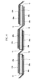
- Fig. 11 shows that front and back surfaces of neighboring solar cells are connected using a single-side-corrugated tab.
- the vertex portions face the front side of solar cell 1 and the flat portion faces the back side. Accordingly, the vertex portions of tab 20 on the front side bite electrode 11. However, the tab 20 does not bite back electrode 12 on the back side of solar cell 1.
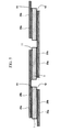
- Fig. 5 shows that the front surfaces of two neighboring solar cells 1 are connected with each other and the back surfaces thereof are also connected with each other by tabs 20.
- tabs 20 even when the single-side-corrugated tab is used, the vertex portions of tab 20 can be cause to bite both of front electrode 11 and back electrode 12.
- two neighboring solar cells 1 are connected in parallel and pairs of solar cells 1 arranged in parallel are connected in series.
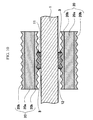
- Fig. 8 shows that front and back surfaces of neighboring solar cells are connected using double-side-corrugated tabs.
- the vertex portions of tabs 20 face both of front electrode 11 and back electrode 12 of solar cell 1. Accordingly, as shown in Fig. 10 , the vertex portions of tabs 20 on the front and back sides bite both of front electrode 11 and back electrode 12.
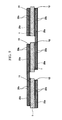
- Fig. 9 shows that the front surfaces of two neighboring solar cells 1 are connected with each other and the back surfaces thereof are also connected with each other by double-side-corrugated tabs.
- two neighboring solar cells 1 are connected in parallel and pairs of solar cells 1 arranged in parallel are connected in series.
- a solar cell module of the invention and a solar cell module of a reference example are prepared and a temperature cycling test is performed.
- the temperature cycling test is performed under the conditions in which a temperature is raised from ordinary temperature to 90 ⁇ 2°C, then lowered to -40°C ⁇ 3°C, and returned to the ordinary temperature, each of upper limit temperature and lower limit temperature is maintained for 10 minutes or longer, one cycle is 6 hours or shorter, a temperature change rate is set at 87°C/hour both in temperature increasing and decreasing processes. This temperature cycling is repeated at 400 cycles. As shown in Fig.
- the reference example uses as tab 20 one provided with tin coating layer 20b as a soft conductive body on the surface of copper foil 20a, and is connected with front electrode 11 and back electrode 12 by using the aforementioned anisotropic conductive adhesive.
- tab 20 coated with tin is not provided with corrugations.
- a single-side-corrugated tab provided with silver layer 20b is used on the front side and tin coating layer 20b as a soft conductive body covering the surface of copper foil 20a is provided on the back side.
- both sides of one solar cell 1 are connected with relevant tabs 20, and then solar cell 1 is sandwiched between translucent sealing material sheets such as EVA and placed between a front member made of glass and a back member made of a weather resistant film. Then, the solar cell is sealed by the sealing material between the front member and the back member by the laminator.
- translucent sealing material sheets such as EVA
- Table 1 shows results of performing the test of 400 thermal cycles.
- Table 1 shows a decreasing rate based on output values in a conventional example and example 1. Note that the decreasing rate is normalized by using the reference example as 1. From Table 1, it can be seen that the decreasing rate even after 400 thermal cycles is greatly decreased to 0.44, owing to the configuration in which silver layer 20b of tab 20 bites front electrode 11.
- example 1 and example 2 of the invention are prepared and examined by the test of 600 thermal cycles.
- Example 2 uses double-side-corrugated tabs 20 and silver layer 20b bites both of front electrode 11 and back electrode 12 as shown in Fig. 10 .
- Table 2 shows the results.
- a decreasing rate is shown based on output values in the examples. Note that the decreasing rate is normalized by using example 1 as 1. From Table 2, it can be seen that use of a double-side-corrugated tab 20 is more effective because the decrease rate even after 600 thermal cycles is 0.74 with respect to the one using single-side tab 20.
- the tab bites the front electrode and back electrode as described above. This configuration is considered to generate anchor effects to suppress the movement of the tab in thermal expansion or thermal contraction of the tab, and thereby to enhance the reliability against temperature change.
- Solar cells usable as solar cell 1 in the invention include, for example, a solar cell having a so-called HIT (registered trademark) structure in which a non-crystalline silicon layer is stacked on a surface of a crystalline silicon substrate, or a normal crystalline or thin-film solar cell.
- HIT registered trademark
- bus bar electrodes 111, 121 in the above-described embodiment are each formed in the form of a zigzag line, but the invention can be applied to even a case where bus bar electrodes are in the form of a straight line.
- the electrode includes finger electrodes and bus bar electrodes.
- the invention can be applied even in a solar cell only having finger electrodes as an electrode.
- the material for the tab is a copper foil in the description of the embodiment, any material having low electric resistance can be used for the tab. Besides copper, iron, nickel, silver or a combination thereof can provide similar effects.
- the core and the surface are formed of different materials.
- the invention can be applied to a tab in which the core and the surface are formed of a same material.
Landscapes
- Photovoltaic Devices (AREA)
- Engineering & Computer Science (AREA)
- Manufacturing & Machinery (AREA)
- Life Sciences & Earth Sciences (AREA)
- Sustainable Development (AREA)
Abstract
Description
- The invention relates to a solar cell module and a method of manufacturing a solar cell module.
- A solar cell module has a configuration in which a plurality of solar cells are connected in series and/or parallel by wiring members electrically connected with electrodes on front and back surfaces of the solar cells. In manufacturing solar cell modules, soldering is conventionally used to connect the electrodes and the wiring members of the solar cells with each other. The soldering is widely used because being excellent in conductivity and connection reliability such as fixing strength, and having inexpensive and versatile characteristics.
- On the other hand, a wiring connection method for a solar cell without using soldering has been also considered to decrease heat affect during the process of connecting a wiring member. For example, there is known a method of connecting a solar cell with a wiring member by using an adhesive film having a rein adhesive (see, for example, Patent Document 1).
- In the wiring connection using the adhesive film, a wiring member is connected with an electrode of a solar cell by a resin adhesive in such a manner that the wiring member and the solar cell are heated while being pressed against each other with the adhesive film disposed between the wiring member and the electrode of the solar cell.
- As one of the aforementioned solar cell modules using the resin adhesive, there has been proposed a solar cell module in which a bus bar electrode formed on the surface of the solar cell is buried in a wiring member in order to prevent the electrode and the wiring member from peeling off each other (for example, Patent Document 2). The wiring member is provided with a soft conductor layer, such as soldering, around a copper foil so that the bus bar electrode can be buried easily.
-
- Patent Document 1: Japanese Patent Application Publication No.
2007-214533 - Patent Document 2: Domestic Re-publication of PCT International Application
WO2008/023795 - The solar cell module described in Patent Document 2 has sufficient electrode-peel strength, but is still required to enhance the reliability under thermal cycles.
- In view of the above-described requirement, an objective of the invention is to enhance a solar cell output by preventing a wiring member from peeling off in thermal cycles.
- The invention provides a solar cell module including a plurality of solar cells connected with one another by connecting electrodes formed on surfaces of neighboring solar cells by wiring members, wherein a portion of the wiring members bites the electrodes and the solar cells and the tabs are bonded with each other by a resin.
- In addition, the invention includes the steps of: forming an electrode on a surface of a solar cell; disposing a wiring member on a resin disposed to cover the electrode, the wiring member being to be connected with an electrode formed on a surface of a neighboring solar cell; and heating the solar cell while applying pressure in a direction toward the solar cell from above the wiring member, and thereby causing a portion of the wiring member to bite the electrode. Here, the surface of the wiring member is harder than the surface of the electrode.
- The invention can provide a solar cell module with high reliability in which a portion of a wiring member bites an electrode to maintain tab strength even in thermal cycles.
-
- [
Fig. 1] Fig. 1 is a plan view of solar cells in a solar cell module according to an embodiment of the invention. - [
Fig. 2] Fig. 2 is a schematic plan view showing a solar cell according to the embodiment of the invention. - [
Fig. 3] Fig. 3 is a schematic plan view showing that tabs are bonded to a solar cell in the embodiment of the invention. - [
Fig. 4] Fig. 4 is a cross-sectional view taken along the A-A' line inFig. 1 . - [
Fig. 5] Fig. 5 is a schematic cross-sectional view in the embodiment of the invention. - [
Fig. 6] Fig. 6 is a schematic cross-sectional view showing that a tab is bonded to a solar cell in the embodiment of the invention. - [
Fig. 7] Fig. 7 is a schematic plan view showing that a tab is bonded to a solar cell in the embodiment of the invention. - [
Fig. 8] Fig. 8 is a schematic cross-sectional view in the embodiment of the invention. - [
Fig. 9] Fig. 9 is a schematic cross-sectional view in the embodiment of the invention. - [
Fig. 10] Fig. 10 is a schematic cross-sectional view showing that tabs are bonded to a solar cell in the embodiment of the invention. - [
Fig. 11] Fig. 11 is a schematic cross-sectional view showing that tabs are bonded to a solar cell in the embodiment of the invention. - [
Fig. 12] Fig. 12 is a schematic cross-sectional view showing that tabs are bonded to a conventional solar cell. - [
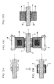
Fig. 13] Fig. 13 is a schematic view showing how to bond tabs according to the invention. - Solar cell modules according to embodiments of the invention are described in detail by referring to the drawings. Note that same reference numerals are given to same or equivalent portions in the drawings, and the description thereof is not repeated for avoiding duplicated description.
-
Fig. 1 is a solar cell module according to the present embodiment. As shown inFig. 1 , the solar cell module includes a plurality of plate-likesolar cells 1. The solar cell is made of a crystalline semiconductor including, for example, a single crystal silicon or polycrystalline silicon with a thickness of approximately 0.15 mm and has a substantially square shape with one side of 125 mm. However, the thickness, size and the like are not limited to those and a solar cell with another configuration may be used. - For example, in
solar cell 1, an n-type region and a p-type region are formed to form a semiconductor junction for generating an electric field for carrier separation in an interface portion between the n-type region and the p-type region. - As shown in
Fig. 2 ,front electrode 11 is formed on a surface on a light-receiving side (front side) ofsolar cell 1, andback electrode 12 is formed on a surface of the back side. In the embodiment,front electrode 11 includes a plurality offinger electrodes 110 formed in parallel to one another. For example, approximately 55finger electrodes 110 are formed with a finger electrode width of approximately 100 µm and a pitch of approximately 2 mm. As shown inFig. 3 ,tabs 20 as wiring members are connected withfinger electrodes 110 at right angles.Bus bar electrodes 111 are provided onfront electrode 11 at positions wheretabs 20 are to be connected.Bus bar electrodes 111 are electrically connected with allfinger electrodes 110.Bus bar electrodes 111 are each formed in the form of a zigzag line in order to have preferable properties of bonding withtabs 20 and provide preferable electric connection betweenfinger electrodes 110 andtabs 20. - Also,
back electrode 12 is formed on a surface portion on a back side ofsolar cell 1.Back electrode 12 includes a plurality offinger electrodes 120 formed in parallel to one another. For example, approximately 217finger electrodes 120 are formed with a finger electrode width of approximately 100 µm and a pitch of approximately 0.5 mm.Bus bar electrodes 121 are provided onback electrode 12 at positions wheretabs 20 are to be connected.Bus bar electrodes 121 are electrically connected with allfinger electrodes 120. Bus bar electrodes 112 are each formed in the form of a zigzag line in order to have preferable properties of bonding withtabs 20 and provide preferable electric connection betweenfinger electrodes 120 andtabs 20. - Such
front electrode 11 andback electrode 12 can be formed by screen painting of a thermosetting or heat burning silver paste, for example. Instead of this, they may be formed using other methods such as a deposition, sputtering, and plating method. - In
Fig. 2 , dots depicted in a region where bus bar electrodes 111 (121) and finger electrodes 110 (120) are connected withtabs 20 schematically show spots where vertex portions oftabs 20 bite the electrodes, which is described later. Also, dots depicted intabs 20 inFig. 3 schematically show spots where vertex portions bite the electrodes.Tabs 20 have such a small width that angled portions ofbus bar electrodes 111 can be exposed fromtabs 20. Accordingly,tabs 20 andbus bar electrodes 111 are easily aligned with each other. - As shown in
Fig. 1 , threetabs 20 are connected on top offront electrode 11 andback electrode 12. A width oftab 20 is approximately 1.5 mm. - Note that, in order to increase an amount of light entering the light-receiving surface of
solar cell 1, the number offinger electrodes 110 offront electrode 11 is set smaller than the number offinger electrodes 120 ofback electrode 12. Also, a thickness offinger electrode 110 offront electrode 11 is set larger than a thickness offinger electrode 120 ofback electrode 12, so that resistance infront electrode 11 can be decreased. Thus, solar cell characteristics can be further enhanced. - Hereinafter, a method of manufacturing a solar cell module using
solar cells 1 is described.Fig. 4 is a cross-sectional view taken along the A-A' line inFig. 1 . In the solar cell module,tabs 20 as wiring members are electrically connected withfront electrode 11 and backelectrode 12 as shown inFig. 1 andFig. 4 .Resin member 3 is used for connectingtabs 20 withfront electrode 11 and backelectrode 12. For example, an anisotropic conductive resin member may be used asresin member 3. - An anisotropic conductive resin member includes at least a resin adhesive component and conductive particles dispersed therein. The resin adhesive component includes a composition containing a thermosetting resin. Resins usable as the resin adhesive component are, for example, epoxy resins, phenoxy resins, acryl resins, polyimide resins, polyamide resins, polycarbonate resins, urethane resins, and the like. Among these thermosetting resins, one kind or a combination of two or more kinds of resins are used, and a preferable thermosetting resin is made of one or more kinds of resins selected from the group consisting of epoxy resins, phenoxy resins, and acryl resins.
- As the conductive particles, used are, for example, metal particles such as gold particles, silver particles, copper particles and nickel particles, or conductive particles, such as gold plating particles, copper plating particles or nickel plating particles in which the surfaces of conductive or insulating core particles are coated with a conductive layer such as a metal layer.
- Firstly,
resin member 3 is disposed between front andback electrodes tab 20. It is preferable thatresin member 3 have the same or smaller width than a width oftab 20 to be connected. For example, if the width oftab 20 is 0.5 mm to 3 mm, the width ofresin member 3 is set to 0.5 mm to 3 mm, or slightly smaller, corresponding to the width oftab 20. In the embodiment, threetabs 20 each having a width of 1.2 mm are used as shown inFig. 1 . Accordingly, threeresin members 3 each having a width corresponding to the width oftab 20 are disposed on positions wheretabs 20 are to be bonded. Note thatresin member 3 may have a larger width than the width oftab 20 ifresin member 3 has translucency even after being cured by heat. - As shown in
Fig. 6 ,tab 20 includes copperthin plate 20a as a core andsilver layer 20b provided on the surface oftab 20.Silver layer 20b forms a layer harder thanfront electrode 11 and backelectrode 12. -
Tab 20 is provided with fine corrugations on at least one side thereof and has a height of approximately 10 to 50 µm in vertex portions of the corrugations.Tab 20 shown inFig. 6 is provided with fine corrugations on one side and a flat surface on the other side. This type of tab is called a single-side-corrugated tab.Tan 20 shown inFig. 10 is provided with fine corrugations on both sides. This type of tab is called a double-side-corrugated tab. The corrugations of the tab can be formed by using grooves extending in a longitudinal direction oftab 20, many pyramid-shaped projections formed on the surface, or the like. -
Tab 20 in whichsilver layer 20b is provided on the surface having the fine corrugations is pressed againstresin member 3, and is heated while being pressed to cureresin member 3 by heat, so thattab 20 is connected withfront electrode 11 and backelectrode 12. - To electrically connect a plurality of neighboring
solar cells 1 with each other bytabs 20,tab 20 is placed on each ofresin members 3 provided on both sides ofsolar cell 1 in such a manner that one end side oftab 20 is connected withfront electrode 11 on the light-receiving surface side of certainsolar cell 1 and the other end side is connected withback electrode 12 on the back side of another solar cell neighboring certainsolar cell 1. - As shown in
Figs. 13A to 13D ,solar cell 1 is prepared (Fig. 13A ) andresin members 3 are placed onfront electrode 11 and backelectrode 12 of solar cell 1 (Fig. 13B ). Then,solar cell 1 placed onheat block 6, for example, is pressed using anotherheat block 6 with a pressure of approximately 0.05 to 1.00 MPa, for example, and therebytab 20 is pressed towardsolar cell 1 withresin members 3 interposed in between (Fig. 13C ). Then, high-temperature heating is performed with a temperature ofheat block 6 set high for thermosetting of a resin adhesive component ofresin member 3, for example, a temperature between 120°C and 200°C, both inclusive. Thus, fixtabs 20 are fixed by compression bonding, so thatsolar cells 1 are electrically connected and arranged (Fig. 13D ). -
Solar cell 1 is heated under pressure in a direction towardsolar cell 1 fromabove tabs 20 disposed onresin member 3. In this heating process, the surface region ofsilver layer 20b oftab 20 remains harder thanfront electrode 11 and backelectrode 12. - Thus, as shown in
Figs. 6 ,7 , and 13(d), the vertex portions (projection portions) oftab 20bite front electrode 11 and backelectrode 12, andtab 20 is bonded tofront electrode 11 and backelectrode 12 byresin member 3. In this way,silver layer 20b having the vertex portions causes the electrodes (bus bar electrodes 111, 121) formed of a solidified epoxy resin mainly containing silver particles to bite both offront electrode 11 and backelectrode 12 - Similarly, second
solar cell 1 is placed ontabs 20 and is fixed with light pressure. Then, the bonding is performed in the same procedures as the above. A desired number ofsolar cells 1 are joined to one another to form a string, and consequently a solar cell module is formed. - The warpage of
solar cell 1 is considered to occur due to a difference in linear expansion coefficient betweentab 20 andsolar cell 1. Since such warpage is proportional to temperature, a higher temperature applied totab 20 andsolar cell 1 is likely to cause larger warpage ofsolar cell 1. Accordingly, it can be said that the most effective way to reduce the warpage ofsolar cell 1 is adhesive bonding at a low temperature. - Since the solar cell module according to the embodiment uses
resin member 3 capable of bonding at a lower temperature than an alloy bonding by soldering, stress due to the warpage on front and back surfaces ofsolar cell 1 can be made smaller and occurrence of the warpage can be prevented. - Furthermore, since
resin member 3 adhere to the surroundings ofsilver layer 20b oftab 20 bitingfront electrode 11 and backelectrode 12, the bonding strength oftab 20 can be increased. - Note that an anisotropic conductive resin member is shown as an example of
resin member 3 in the above-described embodiment, but one not containing conductive particles can be used asresin member 3. When a resin member not containing conductive particles is used asresin member 3, part of the surfaces offront electrode 11 and backelectrode 12 is brought into direct contact with the surface oftabs 20, and thereby front andsecond electrodes tabs 20 are electrically connected with each other. Even in this case,silver layer 20b oftab 20 bitesfront electrode 11 and backelectrode 12, and thus sufficient electric connection can be obtained. - In this manner, the plurality of
solar cells 1 connected with each other bytabs 20 are sandwiched between translucent sealing material sheets such as EVA, and then placed between a front member made of glass and a back member made of a weather resistant film or a glass or plastic material. Then,solar cells 1 are sealed by the sealing material between the front member and the back member by a laminator. Consequently, a solar cell module is obtained. -
Fig. 11 shows that front and back surfaces of neighboring solar cells are connected using a single-side-corrugated tab. In this example, the vertex portions face the front side ofsolar cell 1 and the flat portion faces the back side. Accordingly, the vertex portions oftab 20 on the frontside bite electrode 11. However, thetab 20 does not bite backelectrode 12 on the back side ofsolar cell 1. -
Fig. 5 shows that the front surfaces of two neighboringsolar cells 1 are connected with each other and the back surfaces thereof are also connected with each other bytabs 20. In this example, even when the single-side-corrugated tab is used, the vertex portions oftab 20 can be cause to bite both offront electrode 11 and backelectrode 12. In this example, two neighboringsolar cells 1 are connected in parallel and pairs ofsolar cells 1 arranged in parallel are connected in series. -
Fig. 8 shows that front and back surfaces of neighboring solar cells are connected using double-side-corrugated tabs. In this example, the vertex portions oftabs 20 face both offront electrode 11 and backelectrode 12 ofsolar cell 1. Accordingly, as shown inFig. 10 , the vertex portions oftabs 20 on the front and back sides bite both offront electrode 11 and backelectrode 12. -
Fig. 9 shows that the front surfaces of two neighboringsolar cells 1 are connected with each other and the back surfaces thereof are also connected with each other by double-side-corrugated tabs. In this example, two neighboringsolar cells 1 are connected in parallel and pairs ofsolar cells 1 arranged in parallel are connected in series. - Next, a solar cell module of the invention and a solar cell module of a reference example are prepared and a temperature cycling test is performed. The temperature cycling test is performed under the conditions in which a temperature is raised from ordinary temperature to 90 ± 2°C, then lowered to -40°C ± 3°C, and returned to the ordinary temperature, each of upper limit temperature and lower limit temperature is maintained for 10 minutes or longer, one cycle is 6 hours or shorter, a temperature change rate is set at 87°C/hour both in temperature increasing and decreasing processes. This temperature cycling is repeated at 400 cycles. As shown in
Fig. 12 , the reference example uses astab 20 one provided withtin coating layer 20b as a soft conductive body on the surface ofcopper foil 20a, and is connected withfront electrode 11 and backelectrode 12 by using the aforementioned anisotropic conductive adhesive. Note thattab 20 coated with tin is not provided with corrugations. As shown inFig. 11 , in example 1 of the invention, a single-side-corrugated tab provided withsilver layer 20b is used on the front side andtin coating layer 20b as a soft conductive body covering the surface ofcopper foil 20a is provided on the back side. - In the solar cell module used in this test, both sides of one
solar cell 1 are connected withrelevant tabs 20, and thensolar cell 1 is sandwiched between translucent sealing material sheets such as EVA and placed between a front member made of glass and a back member made of a weather resistant film. Then, the solar cell is sealed by the sealing material between the front member and the back member by the laminator. - Table 1 shows results of performing the test of 400 thermal cycles.
-
[Table 1] Front tab Back tab Decreasing rate after 400 thermal cycles Reference example Conventional (soldering) tab Conventional (soldering) tab 1 Example 1 Silver tab corrugated surface bonding Soldering tab 0.44 - Table 1 shows a decreasing rate based on output values in a conventional example and example 1. Note that the decreasing rate is normalized by using the reference example as 1. From Table 1, it can be seen that the decreasing rate even after 400 thermal cycles is greatly decreased to 0.44, owing to the configuration in which
silver layer 20b oftab 20 bitesfront electrode 11. - Next, example 1 and example 2 of the invention are prepared and examined by the test of 600 thermal cycles. Example 2 uses double-side-corrugated
tabs 20 andsilver layer 20b bites both offront electrode 11 and backelectrode 12 as shown inFig. 10 . Table 2 shows the results. -
[Table 2] Front tab Back tab Decreasing rate after 600 thermal cycles Example 1 Silver tab corrugated surface bonding Soldering tab 1 Example 2 Silver tab Silver tab 0.74 corrugated surface bonding corrugated surface bonding - A decreasing rate is shown based on output values in the examples. Note that the decreasing rate is normalized by using example 1 as 1. From Table 2, it can be seen that use of a double-side-corrugated
tab 20 is more effective because the decrease rate even after 600 thermal cycles is 0.74 with respect to the one using single-side tab 20. - In the invention, the tab bites the front electrode and back electrode as described above. This configuration is considered to generate anchor effects to suppress the movement of the tab in thermal expansion or thermal contraction of the tab, and thereby to enhance the reliability against temperature change.
- Solar cells usable as
solar cell 1 in the invention include, for example, a solar cell having a so-called HIT (registered trademark) structure in which a non-crystalline silicon layer is stacked on a surface of a crystalline silicon substrate, or a normal crystalline or thin-film solar cell. - In addition,
bus bar electrodes - Also, in the above-described embodiment, the electrode includes finger electrodes and bus bar electrodes. However, the invention can be applied even in a solar cell only having finger electrodes as an electrode.
- Moreover, although the material for the tab is a copper foil in the description of the embodiment, any material having low electric resistance can be used for the tab. Besides copper, iron, nickel, silver or a combination thereof can provide similar effects.
- Furthermore, in the tab in the embodiment, the core and the surface are formed of different materials. However, the invention can be applied to a tab in which the core and the surface are formed of a same material.
- It should be understood that all the aspects of the embodiments disclosed herein are only for illustrative purposes and are not intended to impose limitation. The scope of the invention is defined not by the description of the above embodiments but by the scope of claims, and the invention is intended to include equivalents to any in the scope of claims and all modifications within the scope of claims.
-
- 1
- Solar cell
- 3
- Resin layer
- 11
- Front electrode
- 12
- Back electrode
- 20
- Tab
- 20a
- Copper foil
- 20b
- Silver layer
Claims (4)
- A solar cell module comprising: a plurality of solar cells connected with one another in such a manner that electrodes formed on surfaces of neighboring solar cells are connected with each other through a wiring member, wherein
a portion of the wiring member bites the electrodes, and
the solar cells and the wiring member are bonded to each other by a resin. - The solar cell module according to claim 1, wherein the wiring member has a corrugated portion formed on at least one side, the corrugated portion being harder than a surface of the electrode.
- A method of manufacturing a solar cell module, comprising:forming an electrode on a surface of a solar cell;disposing a wiring member on a resin to cover the electrode, the wiring member being to be connected with an electrode formed on a surface of a neighboring solar cell; andheating the solar cell while applying pressure in a direction toward the solar cell from above the wiring member, and thereby causing a portion of the wiring member to bite the electrode, whereinthe surface of the wiring member is harder than the surface of the electrode.
- The method of manufacturing a solar cell module according to claim 3, wherein the wiring member includes a corrugated portion formed on at least one side.
Applications Claiming Priority (2)
| Application Number | Priority Date | Filing Date | Title |
|---|---|---|---|
| JP2010125230 | 2010-05-31 | ||
| PCT/JP2011/062259 WO2011152319A1 (en) | 2010-05-31 | 2011-05-27 | Solar cell module and solar cell module manufacturing method |
Publications (3)
| Publication Number | Publication Date |
|---|---|
| EP2579332A1 true EP2579332A1 (en) | 2013-04-10 |
| EP2579332A4 EP2579332A4 (en) | 2017-10-25 |
| EP2579332B1 EP2579332B1 (en) | 2021-02-17 |
Family
ID=45066686
Family Applications (1)
| Application Number | Title | Priority Date | Filing Date |
|---|---|---|---|
| EP11789722.3A Not-in-force EP2579332B1 (en) | 2010-05-31 | 2011-05-27 | Solar cell module and solar cell module manufacturing method |
Country Status (4)
| Country | Link |
|---|---|
| US (1) | US8927851B2 (en) |
| EP (1) | EP2579332B1 (en) |
| JP (2) | JP5991534B2 (en) |
| WO (1) | WO2011152319A1 (en) |
Cited By (1)
| Publication number | Priority date | Publication date | Assignee | Title |
|---|---|---|---|---|
| EP2631953A2 (en) * | 2012-02-23 | 2013-08-28 | LG Electronics Inc. | Solar cell module |
Families Citing this family (8)
| Publication number | Priority date | Publication date | Assignee | Title |
|---|---|---|---|---|
| US20160064587A1 (en) * | 2013-04-25 | 2016-03-03 | Panasonic Intellectual Property Management Co., Ltd. | Solar cell module and method for manufacturing solar cell module |
| JP6511736B2 (en) * | 2014-06-20 | 2019-05-15 | 日立化成株式会社 | Method of manufacturing solar cell module |
| US9741878B2 (en) * | 2015-11-24 | 2017-08-22 | PLANT PV, Inc. | Solar cells and modules with fired multilayer stacks |
| WO2017091782A1 (en) * | 2015-11-24 | 2017-06-01 | Plant Pv, Inc | Fired multilayer stacks for use in integrated circuits and solar cells |
| WO2017179523A1 (en) * | 2016-04-14 | 2017-10-19 | 株式会社カネカ | Solar cell wiring member and solar cell module |
| JP6915054B2 (en) * | 2017-05-10 | 2021-08-04 | シャープ株式会社 | Photoelectric conversion device and solar cell module equipped with it |
| JP6705517B2 (en) * | 2019-02-01 | 2020-06-03 | 日立化成株式会社 | Method for manufacturing solar cell module |
| CN115602745A (en) * | 2022-10-27 | 2023-01-13 | 安徽华晟新能源科技有限公司(Cn) | Solder strip piece, manufacturing method thereof and photovoltaic module |
Family Cites Families (13)
| Publication number | Priority date | Publication date | Assignee | Title |
|---|---|---|---|---|
| US4301322A (en) * | 1980-04-03 | 1981-11-17 | Exxon Research & Engineering Co. | Solar cell with corrugated bus |
| JP3319697B2 (en) * | 1996-11-29 | 2002-09-03 | 太陽誘電株式会社 | Wound electronic component and method of manufacturing the same |
| US6586270B2 (en) * | 2000-06-01 | 2003-07-01 | Canon Kabushiki Kaisha | Process for producing a photovoltaic element |
| JP2006278710A (en) * | 2005-03-29 | 2006-10-12 | Kyocera Corp | Solar cell module and manufacturing method thereof |
| US7476800B2 (en) * | 2005-06-01 | 2009-01-13 | Outokumpu Copper Neumayer Gmbh | Electric connection element |
| JP2007214533A (en) | 2006-01-16 | 2007-08-23 | Hitachi Chem Co Ltd | Conductive bonding film and solar cell module |
| TWI487124B (en) | 2006-08-25 | 2015-06-01 | Sanyo Electric Co | Solar battery module and solar battery module manufacturing method |
| JP4294048B2 (en) * | 2006-11-29 | 2009-07-08 | 三洋電機株式会社 | Solar cell module |
| KR101081706B1 (en) * | 2007-05-09 | 2011-11-09 | 히다치 가세고교 가부시끼가이샤 | Method for connecting conductor, member for connecting conductor, connecting structure and solar cell module |
| JP5115553B2 (en) * | 2007-05-09 | 2013-01-09 | 日立化成工業株式会社 | Conductor connection member, connection structure, and solar cell module |
| WO2009041506A1 (en) * | 2007-09-26 | 2009-04-02 | Hitachi Chemical Company, Ltd. | Member for conductor connection, method for manufacturing the same, connection structure, and solar cell module |
| TWI438915B (en) | 2008-02-21 | 2014-05-21 | Sanyo Electric Co | Solar battery module |
| EP2287959A1 (en) * | 2008-05-27 | 2011-02-23 | Fujikura, Ltd. | Photoelectric conversion element |
-
2011
- 2011-05-27 EP EP11789722.3A patent/EP2579332B1/en not_active Not-in-force
- 2011-05-27 WO PCT/JP2011/062259 patent/WO2011152319A1/en not_active Ceased
- 2011-05-27 JP JP2012518367A patent/JP5991534B2/en not_active Expired - Fee Related
-
2012
- 2012-11-21 US US13/683,131 patent/US8927851B2/en not_active Expired - Fee Related
-
2015
- 2015-09-29 JP JP2015190655A patent/JP6043971B2/en not_active Expired - Fee Related
Non-Patent Citations (1)
| Title |
|---|
| See references of WO2011152319A1 * |
Cited By (1)
| Publication number | Priority date | Publication date | Assignee | Title |
|---|---|---|---|---|
| EP2631953A2 (en) * | 2012-02-23 | 2013-08-28 | LG Electronics Inc. | Solar cell module |
Also Published As
| Publication number | Publication date |
|---|---|
| EP2579332A4 (en) | 2017-10-25 |
| JPWO2011152319A1 (en) | 2013-08-01 |
| JP5991534B2 (en) | 2016-09-14 |
| JP6043971B2 (en) | 2016-12-14 |
| US20130125951A1 (en) | 2013-05-23 |
| WO2011152319A1 (en) | 2011-12-08 |
| JP2016006913A (en) | 2016-01-14 |
| EP2579332B1 (en) | 2021-02-17 |
| US8927851B2 (en) | 2015-01-06 |
Similar Documents
| Publication | Publication Date | Title |
|---|---|---|
| US10896984B2 (en) | Solar cell module | |
| EP2579332B1 (en) | Solar cell module and solar cell module manufacturing method | |
| CN102122677B (en) | Solar battery module and solar battery module manufacturing method | |
| JP5380810B2 (en) | Solar cell module | |
| EP2472597A1 (en) | Solar cell string and solar cell module using same | |
| CN103797588B (en) | Manufacturing method of solar cell module, method of connecting solar cell module and ribbon | |
| JP5923732B2 (en) | Solar cell module | |
| JP5046743B2 (en) | Solar cell module and manufacturing method thereof | |
| EP2579324B1 (en) | Solar cell module and method for manufacturing same | |
| JP2006278710A (en) | Solar cell module and manufacturing method thereof | |
| US20130104961A1 (en) | Solar cell module and solar cell | |
| US9117953B2 (en) | Solar cell module and solar cell | |
| WO2013154188A1 (en) | Solar cell | |
| EP2590228A1 (en) | Solar cell module and method for manufacturing same | |
| JP2008085227A (en) | Solar cell module | |
| JP2011108982A (en) | Solar cell module | |
| JP5499729B2 (en) | Manufacturing method of solar cell module | |
| WO2023239292A2 (en) | Soft spacers for shingled solar cell panels |
Legal Events
| Date | Code | Title | Description |
|---|---|---|---|
| PUAI | Public reference made under article 153(3) epc to a published international application that has entered the european phase |
Free format text: ORIGINAL CODE: 0009012 |
|
| 17P | Request for examination filed |
Effective date: 20121218 |
|
| AK | Designated contracting states |
Kind code of ref document: A1 Designated state(s): AL AT BE BG CH CY CZ DE DK EE ES FI FR GB GR HR HU IE IS IT LI LT LU LV MC MK MT NL NO PL PT RO RS SE SI SK SM TR |
|
| DAX | Request for extension of the european patent (deleted) | ||
| RAP1 | Party data changed (applicant data changed or rights of an application transferred) |
Owner name: PANASONIC INTELLECTUAL PROPERTY MANAGEMENT CO., LT |
|
| REG | Reference to a national code |
Ref country code: DE Ref legal event code: R079 Ref document number: 602011070147 Country of ref document: DE Free format text: PREVIOUS MAIN CLASS: H01L0031042000 Ipc: H01L0031050000 |
|
| RA4 | Supplementary search report drawn up and despatched (corrected) |
Effective date: 20170927 |
|
| RIC1 | Information provided on ipc code assigned before grant |
Ipc: H01L 31/068 20120101ALI20170921BHEP Ipc: H01L 31/05 20140101AFI20170921BHEP |
|
| GRAP | Despatch of communication of intention to grant a patent |
Free format text: ORIGINAL CODE: EPIDOSNIGR1 |
|
| STAA | Information on the status of an ep patent application or granted ep patent |
Free format text: STATUS: GRANT OF PATENT IS INTENDED |
|
| INTG | Intention to grant announced |
Effective date: 20201116 |
|
| GRAS | Grant fee paid |
Free format text: ORIGINAL CODE: EPIDOSNIGR3 |
|
| GRAA | (expected) grant |
Free format text: ORIGINAL CODE: 0009210 |
|
| STAA | Information on the status of an ep patent application or granted ep patent |
Free format text: STATUS: THE PATENT HAS BEEN GRANTED |
|
| AK | Designated contracting states |
Kind code of ref document: B1 Designated state(s): AL AT BE BG CH CY CZ DE DK EE ES FI FR GB GR HR HU IE IS IT LI LT LU LV MC MK MT NL NO PL PT RO RS SE SI SK SM TR |
|
| REG | Reference to a national code |
Ref country code: GB Ref legal event code: FG4D |
|
| REG | Reference to a national code |
Ref country code: CH Ref legal event code: EP |
|
| REG | Reference to a national code |
Ref country code: DE Ref legal event code: R096 Ref document number: 602011070147 Country of ref document: DE |
|
| REG | Reference to a national code |
Ref country code: AT Ref legal event code: REF Ref document number: 1362623 Country of ref document: AT Kind code of ref document: T Effective date: 20210315 |
|
| REG | Reference to a national code |
Ref country code: IE Ref legal event code: FG4D |
|
| REG | Reference to a national code |
Ref country code: LT Ref legal event code: MG9D |
|
| REG | Reference to a national code |
Ref country code: NL Ref legal event code: MP Effective date: 20210217 |
|
| PG25 | Lapsed in a contracting state [announced via postgrant information from national office to epo] |
Ref country code: HR Free format text: LAPSE BECAUSE OF FAILURE TO SUBMIT A TRANSLATION OF THE DESCRIPTION OR TO PAY THE FEE WITHIN THE PRESCRIBED TIME-LIMIT Effective date: 20210217 Ref country code: GR Free format text: LAPSE BECAUSE OF FAILURE TO SUBMIT A TRANSLATION OF THE DESCRIPTION OR TO PAY THE FEE WITHIN THE PRESCRIBED TIME-LIMIT Effective date: 20210518 Ref country code: FI Free format text: LAPSE BECAUSE OF FAILURE TO SUBMIT A TRANSLATION OF THE DESCRIPTION OR TO PAY THE FEE WITHIN THE PRESCRIBED TIME-LIMIT Effective date: 20210217 Ref country code: PT Free format text: LAPSE BECAUSE OF FAILURE TO SUBMIT A TRANSLATION OF THE DESCRIPTION OR TO PAY THE FEE WITHIN THE PRESCRIBED TIME-LIMIT Effective date: 20210617 Ref country code: LT Free format text: LAPSE BECAUSE OF FAILURE TO SUBMIT A TRANSLATION OF THE DESCRIPTION OR TO PAY THE FEE WITHIN THE PRESCRIBED TIME-LIMIT Effective date: 20210217 Ref country code: NO Free format text: LAPSE BECAUSE OF FAILURE TO SUBMIT A TRANSLATION OF THE DESCRIPTION OR TO PAY THE FEE WITHIN THE PRESCRIBED TIME-LIMIT Effective date: 20210517 Ref country code: BG Free format text: LAPSE BECAUSE OF FAILURE TO SUBMIT A TRANSLATION OF THE DESCRIPTION OR TO PAY THE FEE WITHIN THE PRESCRIBED TIME-LIMIT Effective date: 20210517 |
|
| REG | Reference to a national code |
Ref country code: AT Ref legal event code: MK05 Ref document number: 1362623 Country of ref document: AT Kind code of ref document: T Effective date: 20210217 |
|
| PG25 | Lapsed in a contracting state [announced via postgrant information from national office to epo] |
Ref country code: SE Free format text: LAPSE BECAUSE OF FAILURE TO SUBMIT A TRANSLATION OF THE DESCRIPTION OR TO PAY THE FEE WITHIN THE PRESCRIBED TIME-LIMIT Effective date: 20210217 Ref country code: PL Free format text: LAPSE BECAUSE OF FAILURE TO SUBMIT A TRANSLATION OF THE DESCRIPTION OR TO PAY THE FEE WITHIN THE PRESCRIBED TIME-LIMIT Effective date: 20210217 Ref country code: NL Free format text: LAPSE BECAUSE OF FAILURE TO SUBMIT A TRANSLATION OF THE DESCRIPTION OR TO PAY THE FEE WITHIN THE PRESCRIBED TIME-LIMIT Effective date: 20210217 Ref country code: LV Free format text: LAPSE BECAUSE OF FAILURE TO SUBMIT A TRANSLATION OF THE DESCRIPTION OR TO PAY THE FEE WITHIN THE PRESCRIBED TIME-LIMIT Effective date: 20210217 Ref country code: RS Free format text: LAPSE BECAUSE OF FAILURE TO SUBMIT A TRANSLATION OF THE DESCRIPTION OR TO PAY THE FEE WITHIN THE PRESCRIBED TIME-LIMIT Effective date: 20210217 |
|
| PG25 | Lapsed in a contracting state [announced via postgrant information from national office to epo] |
Ref country code: IS Free format text: LAPSE BECAUSE OF FAILURE TO SUBMIT A TRANSLATION OF THE DESCRIPTION OR TO PAY THE FEE WITHIN THE PRESCRIBED TIME-LIMIT Effective date: 20210617 |
|
| PG25 | Lapsed in a contracting state [announced via postgrant information from national office to epo] |
Ref country code: SM Free format text: LAPSE BECAUSE OF FAILURE TO SUBMIT A TRANSLATION OF THE DESCRIPTION OR TO PAY THE FEE WITHIN THE PRESCRIBED TIME-LIMIT Effective date: 20210217 Ref country code: AT Free format text: LAPSE BECAUSE OF FAILURE TO SUBMIT A TRANSLATION OF THE DESCRIPTION OR TO PAY THE FEE WITHIN THE PRESCRIBED TIME-LIMIT Effective date: 20210217 Ref country code: CZ Free format text: LAPSE BECAUSE OF FAILURE TO SUBMIT A TRANSLATION OF THE DESCRIPTION OR TO PAY THE FEE WITHIN THE PRESCRIBED TIME-LIMIT Effective date: 20210217 Ref country code: EE Free format text: LAPSE BECAUSE OF FAILURE TO SUBMIT A TRANSLATION OF THE DESCRIPTION OR TO PAY THE FEE WITHIN THE PRESCRIBED TIME-LIMIT Effective date: 20210217 |
|
| REG | Reference to a national code |
Ref country code: DE Ref legal event code: R097 Ref document number: 602011070147 Country of ref document: DE |
|
| PG25 | Lapsed in a contracting state [announced via postgrant information from national office to epo] |
Ref country code: RO Free format text: LAPSE BECAUSE OF FAILURE TO SUBMIT A TRANSLATION OF THE DESCRIPTION OR TO PAY THE FEE WITHIN THE PRESCRIBED TIME-LIMIT Effective date: 20210217 Ref country code: SK Free format text: LAPSE BECAUSE OF FAILURE TO SUBMIT A TRANSLATION OF THE DESCRIPTION OR TO PAY THE FEE WITHIN THE PRESCRIBED TIME-LIMIT Effective date: 20210217 Ref country code: ES Free format text: LAPSE BECAUSE OF FAILURE TO SUBMIT A TRANSLATION OF THE DESCRIPTION OR TO PAY THE FEE WITHIN THE PRESCRIBED TIME-LIMIT Effective date: 20210217 Ref country code: DK Free format text: LAPSE BECAUSE OF FAILURE TO SUBMIT A TRANSLATION OF THE DESCRIPTION OR TO PAY THE FEE WITHIN THE PRESCRIBED TIME-LIMIT Effective date: 20210217 |
|
| PLBE | No opposition filed within time limit |
Free format text: ORIGINAL CODE: 0009261 |
|
| STAA | Information on the status of an ep patent application or granted ep patent |
Free format text: STATUS: NO OPPOSITION FILED WITHIN TIME LIMIT |
|
| REG | Reference to a national code |
Ref country code: CH Ref legal event code: PL |
|
| 26N | No opposition filed |
Effective date: 20211118 |
|
| GBPC | Gb: european patent ceased through non-payment of renewal fee |
Effective date: 20210527 |
|
| PG25 | Lapsed in a contracting state [announced via postgrant information from national office to epo] |
Ref country code: LU Free format text: LAPSE BECAUSE OF NON-PAYMENT OF DUE FEES Effective date: 20210527 Ref country code: MC Free format text: LAPSE BECAUSE OF FAILURE TO SUBMIT A TRANSLATION OF THE DESCRIPTION OR TO PAY THE FEE WITHIN THE PRESCRIBED TIME-LIMIT Effective date: 20210217 Ref country code: LI Free format text: LAPSE BECAUSE OF NON-PAYMENT OF DUE FEES Effective date: 20210531 Ref country code: CH Free format text: LAPSE BECAUSE OF NON-PAYMENT OF DUE FEES Effective date: 20210531 Ref country code: AL Free format text: LAPSE BECAUSE OF FAILURE TO SUBMIT A TRANSLATION OF THE DESCRIPTION OR TO PAY THE FEE WITHIN THE PRESCRIBED TIME-LIMIT Effective date: 20210217 |
|
| REG | Reference to a national code |
Ref country code: BE Ref legal event code: MM Effective date: 20210531 |
|
| PG25 | Lapsed in a contracting state [announced via postgrant information from national office to epo] |
Ref country code: SI Free format text: LAPSE BECAUSE OF FAILURE TO SUBMIT A TRANSLATION OF THE DESCRIPTION OR TO PAY THE FEE WITHIN THE PRESCRIBED TIME-LIMIT Effective date: 20210217 |
|
| PG25 | Lapsed in a contracting state [announced via postgrant information from national office to epo] |
Ref country code: IT Free format text: LAPSE BECAUSE OF FAILURE TO SUBMIT A TRANSLATION OF THE DESCRIPTION OR TO PAY THE FEE WITHIN THE PRESCRIBED TIME-LIMIT Effective date: 20210217 Ref country code: IE Free format text: LAPSE BECAUSE OF NON-PAYMENT OF DUE FEES Effective date: 20210527 Ref country code: GB Free format text: LAPSE BECAUSE OF NON-PAYMENT OF DUE FEES Effective date: 20210527 |
|
| PG25 | Lapsed in a contracting state [announced via postgrant information from national office to epo] |
Ref country code: IS Free format text: LAPSE BECAUSE OF FAILURE TO SUBMIT A TRANSLATION OF THE DESCRIPTION OR TO PAY THE FEE WITHIN THE PRESCRIBED TIME-LIMIT Effective date: 20210617 Ref country code: FR Free format text: LAPSE BECAUSE OF NON-PAYMENT OF DUE FEES Effective date: 20210531 |
|
| PG25 | Lapsed in a contracting state [announced via postgrant information from national office to epo] |
Ref country code: BE Free format text: LAPSE BECAUSE OF NON-PAYMENT OF DUE FEES Effective date: 20210531 |
|
| PG25 | Lapsed in a contracting state [announced via postgrant information from national office to epo] |
Ref country code: HU Free format text: LAPSE BECAUSE OF FAILURE TO SUBMIT A TRANSLATION OF THE DESCRIPTION OR TO PAY THE FEE WITHIN THE PRESCRIBED TIME-LIMIT; INVALID AB INITIO Effective date: 20110527 Ref country code: CY Free format text: LAPSE BECAUSE OF FAILURE TO SUBMIT A TRANSLATION OF THE DESCRIPTION OR TO PAY THE FEE WITHIN THE PRESCRIBED TIME-LIMIT Effective date: 20210217 |
|
| PGFP | Annual fee paid to national office [announced via postgrant information from national office to epo] |
Ref country code: DE Payment date: 20230519 Year of fee payment: 13 |
|
| PG25 | Lapsed in a contracting state [announced via postgrant information from national office to epo] |
Ref country code: MK Free format text: LAPSE BECAUSE OF FAILURE TO SUBMIT A TRANSLATION OF THE DESCRIPTION OR TO PAY THE FEE WITHIN THE PRESCRIBED TIME-LIMIT Effective date: 20210217 |
|
| PG25 | Lapsed in a contracting state [announced via postgrant information from national office to epo] |
Ref country code: MT Free format text: LAPSE BECAUSE OF FAILURE TO SUBMIT A TRANSLATION OF THE DESCRIPTION OR TO PAY THE FEE WITHIN THE PRESCRIBED TIME-LIMIT Effective date: 20210217 |
|
| REG | Reference to a national code |
Ref country code: DE Ref legal event code: R079 Ref document number: 602011070147 Country of ref document: DE Free format text: PREVIOUS MAIN CLASS: H01L0031050000 Ipc: H10F0019900000 |
|
| REG | Reference to a national code |
Ref country code: DE Ref legal event code: R119 Ref document number: 602011070147 Country of ref document: DE |
|
| PG25 | Lapsed in a contracting state [announced via postgrant information from national office to epo] |
Ref country code: DE Free format text: LAPSE BECAUSE OF NON-PAYMENT OF DUE FEES Effective date: 20241203 |
|
| PG25 | Lapsed in a contracting state [announced via postgrant information from national office to epo] |
Ref country code: TR Free format text: LAPSE BECAUSE OF FAILURE TO SUBMIT A TRANSLATION OF THE DESCRIPTION OR TO PAY THE FEE WITHIN THE PRESCRIBED TIME-LIMIT Effective date: 20210217 |