EP2579029A1 - Method for manufacturing semiconductor device - Google Patents
Method for manufacturing semiconductor device Download PDFInfo
- Publication number
- EP2579029A1 EP2579029A1 EP11789613.4A EP11789613A EP2579029A1 EP 2579029 A1 EP2579029 A1 EP 2579029A1 EP 11789613 A EP11789613 A EP 11789613A EP 2579029 A1 EP2579029 A1 EP 2579029A1
- Authority
- EP
- European Patent Office
- Prior art keywords
- chips
- semiconductor
- defective
- mounting substrate
- sic
- Prior art date
- Legal status (The legal status is an assumption and is not a legal conclusion. Google has not performed a legal analysis and makes no representation as to the accuracy of the status listed.)
- Withdrawn
Links
Images


Classifications
-
- G—PHYSICS
- G01—MEASURING; TESTING
- G01N—INVESTIGATING OR ANALYSING MATERIALS BY DETERMINING THEIR CHEMICAL OR PHYSICAL PROPERTIES
- G01N25/00—Investigating or analyzing materials by the use of thermal means
- G01N25/72—Investigating presence of flaws
-
- H—ELECTRICITY
- H10—SEMICONDUCTOR DEVICES; ELECTRIC SOLID-STATE DEVICES NOT OTHERWISE PROVIDED FOR
- H10P—GENERIC PROCESSES OR APPARATUS FOR THE MANUFACTURE OR TREATMENT OF DEVICES COVERED BY CLASS H10
- H10P74/00—Testing or measuring during manufacture or treatment of wafers, substrates or devices
- H10P74/20—Testing or measuring during manufacture or treatment of wafers, substrates or devices characterised by the properties tested or measured, e.g. structural or electrical properties
-
- G—PHYSICS
- G01—MEASURING; TESTING
- G01R—MEASURING ELECTRIC VARIABLES; MEASURING MAGNETIC VARIABLES
- G01R31/00—Arrangements for testing electric properties; Arrangements for locating electric faults; Arrangements for electrical testing characterised by what is being tested not provided for elsewhere
- G01R31/26—Testing of individual semiconductor devices
-
- H—ELECTRICITY
- H10—SEMICONDUCTOR DEVICES; ELECTRIC SOLID-STATE DEVICES NOT OTHERWISE PROVIDED FOR
- H10P—GENERIC PROCESSES OR APPARATUS FOR THE MANUFACTURE OR TREATMENT OF DEVICES COVERED BY CLASS H10
- H10P74/00—Testing or measuring during manufacture or treatment of wafers, substrates or devices
- H10P74/20—Testing or measuring during manufacture or treatment of wafers, substrates or devices characterised by the properties tested or measured, e.g. structural or electrical properties
- H10P74/207—Electrical properties, e.g. testing or measuring of resistance, deep levels or capacitance-voltage characteristics
-
- H—ELECTRICITY
- H10—SEMICONDUCTOR DEVICES; ELECTRIC SOLID-STATE DEVICES NOT OTHERWISE PROVIDED FOR
- H10P—GENERIC PROCESSES OR APPARATUS FOR THE MANUFACTURE OR TREATMENT OF DEVICES COVERED BY CLASS H10
- H10P74/00—Testing or measuring during manufacture or treatment of wafers, substrates or devices
- H10P74/23—Testing or measuring during manufacture or treatment of wafers, substrates or devices characterised by multiple measurements, corrections, marking or sorting processes
-
- H—ELECTRICITY
- H10—SEMICONDUCTOR DEVICES; ELECTRIC SOLID-STATE DEVICES NOT OTHERWISE PROVIDED FOR
- H10W—GENERIC PACKAGES, INTERCONNECTIONS, CONNECTORS OR OTHER CONSTRUCTIONAL DETAILS OF DEVICES COVERED BY CLASS H10
- H10W90/00—Package configurations
-
- H—ELECTRICITY
- H10—SEMICONDUCTOR DEVICES; ELECTRIC SOLID-STATE DEVICES NOT OTHERWISE PROVIDED FOR
- H10W—GENERIC PACKAGES, INTERCONNECTIONS, CONNECTORS OR OTHER CONSTRUCTIONAL DETAILS OF DEVICES COVERED BY CLASS H10
- H10W72/00—Interconnections or connectors in packages
- H10W72/50—Bond wires
- H10W72/541—Dispositions of bond wires
- H10W72/5445—Dispositions of bond wires being orthogonal to a side surface of the chip, e.g. parallel arrangements
-
- H—ELECTRICITY
- H10—SEMICONDUCTOR DEVICES; ELECTRIC SOLID-STATE DEVICES NOT OTHERWISE PROVIDED FOR
- H10W—GENERIC PACKAGES, INTERCONNECTIONS, CONNECTORS OR OTHER CONSTRUCTIONAL DETAILS OF DEVICES COVERED BY CLASS H10
- H10W72/00—Interconnections or connectors in packages
- H10W72/50—Bond wires
- H10W72/541—Dispositions of bond wires
- H10W72/547—Dispositions of multiple bond wires
- H10W72/5475—Dispositions of multiple bond wires multiple bond wires connected to common bond pads at both ends of the wires
-
- H—ELECTRICITY
- H10—SEMICONDUCTOR DEVICES; ELECTRIC SOLID-STATE DEVICES NOT OTHERWISE PROVIDED FOR
- H10W—GENERIC PACKAGES, INTERCONNECTIONS, CONNECTORS OR OTHER CONSTRUCTIONAL DETAILS OF DEVICES COVERED BY CLASS H10
- H10W76/00—Containers; Fillings or auxiliary members therefor; Seals
- H10W76/40—Fillings or auxiliary members in containers, e.g. centering rings
- H10W76/42—Fillings
- H10W76/47—Solid or gel fillings
-
- H—ELECTRICITY
- H10—SEMICONDUCTOR DEVICES; ELECTRIC SOLID-STATE DEVICES NOT OTHERWISE PROVIDED FOR
- H10W—GENERIC PACKAGES, INTERCONNECTIONS, CONNECTORS OR OTHER CONSTRUCTIONAL DETAILS OF DEVICES COVERED BY CLASS H10
- H10W90/00—Package configurations
- H10W90/701—Package configurations characterised by the relative positions of pads or connectors relative to package parts
- H10W90/751—Package configurations characterised by the relative positions of pads or connectors relative to package parts of bond wires
- H10W90/754—Package configurations characterised by the relative positions of pads or connectors relative to package parts of bond wires between a chip and a stacked insulating package substrate, interposer or RDL
Definitions
- This invention relates to a method for manufacturing a semiconductor device using a low-capacity chip.
- SiC Silicon carbide
- Patent Literature 1 In order to use such low-capacity chips in large-current applications, semiconductor devices have been proposed in which numerous small-capacity chips are connected in parallel (see for example Patent Literature 1).
- Patent Literature 1 Japanese Patent Application Laid-open No. 2004-95670
- Patent Literature 1 In a case where the feature disclosed in Patent Literature 1 is used, a large current can be passed by connecting numerous small-capacity SiC diodes in parallel, but the manufacturing yield at the time of mounting worsens, and consequently in order to obtain the required number of semiconductor devices, a greater number of semiconductor devices than the required number must be fabricated.
- a compound semiconductor of SiC or similar cannot be manufactured as a large chip due to the substrate quality, and only small-capacity devices are possible.
- numerous small-capacity chips must be connected in parallel, as for example disclosed in Patent Literature 1. Satisfactory items which have passed inspections are used as the small-capacity chips mounted on a substrate, but heat is applied during mounting, so that even when satisfactory items are used, defects occur in a constant fraction thereof. If the manufacturing yield when mounting one small-capacity chip is a (0 ⁇ a ⁇ 1), then the manufacturing yield when mounting n small-capacity chips to form a large-current device is a n . In this way, there is the problem that when numerous small-capacity chips are mounted to increase the current capacity, the manufacturing yield worsens exponentially.
- This invention has as an object the provision of a method for manufacturing semiconductor devices which enables visual identification of defective chips occurring in a mounting step, and exclusion of the defective chips.
- the method for manufacturing semiconductor devices of one embodiment includes a step of forming, on a substrate, a circuit formed of a plurality of semiconductor elements connected in parallel, and an inspection step of inspecting semiconductor elements forming the circuit, and is characterized in that the inspection step includes a step of applying a voltage to each of the semiconductor elements included in the circuit formed on the substrate, a step of detecting whether there is heat generation in each of the semiconductor elements as a result of the application of a voltage, and a step of severing the connection between a semiconductor element for which heat generation has been detected and another semiconductor element.
- the method for manufacturing semiconductor devices of one embodiment may be characterized in that the semiconductor elements are elements including SiC, GaN, or diamond.
- the method for manufacturing semiconductor devices of one embodiment may be characterized in that the semiconductor elements are diodes or transistors.
- a plurality of diodes or transistors are connected in parallel to configure a semiconductor device, so that even when the current capacities of each of the semiconductor elements are small, a large current capacity is realized for the device overall.
- the method for manufacturing semiconductor devices of one embodiment may be characterized in that the presence of heat generation in each of the semiconductor elements is detected by thermography, by an infrared microscope, or by a temperature sensor.
- thermography or infrared microscope as means to detect the presence of heat generation in a semiconductor element
- the presence of heat generation is detected by analyzing the temperature distribution image generated by these thermal imaging devices.
- thermocouple, thermistor, or other temperature sensor as means of detecting the presence of heat generation in semiconductor elements
- the presence of heat generation is detected by a change in voltage, for example.
- the method for manufacturing semiconductor devices of one embodiment may be characterized in that a thermolabel or thermopaint is attached to each of the semiconductor elements, and the presence of heat generation in each of the semiconductor elements is detected by a change in color of the thermolabels or thermopaint.
- thermolabels the presence of heat generation in each semiconductor element is detected by a change in color of the thermolabels, or thermopaint attached to each of the semiconductor elements.
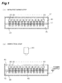
- Fig. 1 is an explanatory diagram explaining in summary the method for manufacturing semiconductor devices in a first embodiment.
- the method for manufacturing semiconductor devices of this embodiment includes a mounting step ( Fig. 1(a) ) of forming, on a mounting substrate 10, a circuit comprising a plurality of SiC semiconductor chips 20 connected in parallel, and an inspection step ( Fig. 1(b) ) of inspecting whether defects have occurred in the mounted SiC semiconductor chips 20.
- a SiC semiconductor chip 20 is a small-capacity chip having a current capacity on the order of 1 to 10 A.
- a semiconductor device for example, a power device
- SiC semiconductor chips 20 are approximately 2 mm on a side, and are disposed in a linear form or a matrix form on the mounting substrate 10, with intervals of several millimeters.
- Fig. 2 is a schematic diagram showing an example of mounting of SiC semieonductor chips 20. In the example shown in Fig.
- SiC diodes in which current flows in the thickness direction, having a front surface electrode 21 and rear surface electrode 22, are used as the mounted SiC semiconductor chips 20.
- the mounting substrate 10 a silicon nitride, aluminum nitride or other insulating substrate 11 with printed wiring (metal faces 12 and 13) on the front and rear surface, can be used.
- the rear surface electrodes 22 of the SiC diodes are fixed using solder or conductive resin to the metal surface 12 on the front surface side of the mounting substrate 10, and the front surface electrodes 21 of the SiC diodes are wired by wire bonds 23 to the metal surface 13 on the rear surface side of the mounting substrate 10, to mount in parallel the plurality of SiC diodes on the mounting substrate 10.
- the mounting substrate 10 with SiC diodes mounted is for example accommodated within a protective case 30 with an upper lid 31, and the space between the mounting substrate 10 and the protective case 30 is packed with a gel 40 having heat-dissipating, moisture-proofing and other properties.
- Fig. 3 is a schematic diagram showing another example of mounting of SiC semiconductor chips 20.
- SiC semiconductor chips 20 SiC diodes having two terminals are used.
- the mounting substrate 10 similarly to the above, a substrate with printed wiring (metal surfaces 12 and 13) formed on both faces of an insulating substrate 11 can be used.
- the two terminals 24 and 25 of the SiC diodes are soldered to the metal surface 12 and 13 on the front-surface side and rear-surface side of the mounting substrate 10 respectively, to mount the plurality of SiC diodes in parallel on the mounting substrate 10.
- the mounting substrata 10 with SiC diodes mounted is for example accommodated within a protective case 30 with an upper lid 31, and the space between the mounting substrate 10 and the protective case 30 is packed with a gel 40 having heat-dissipating, moisture-proofing and other properties.
- the number of SiC semiconductor chips 20 mounted on the mounting substrate 10 is arbitrary, but it is desirable that a greater number of SiC semiconductor chips 20 than necessary be mounted taking into account anticipated defective chips, to satisfy the required current capacity.
- Fig. 2 and Fig. 3 examples are explained in which SiC diodes are mounted as the SiC semiconductor chips 20, but chips to be mounted are not limited to diodes, and transistors may be used.
- Fig. 1(b) In the inspection step shown in Fig. 1(b) , inspections are performed to determine whether defects have occurred in SiC semiconductor chips 20 mounted in the mounting step. Because defective chips cannot be discriminated by external appearance, it is not possible to identify and exclude defective chips visually. A defective chip is electrically short-circuited across the electrodes (terminals), and so in the present embodiment, this is used to identify defective chips. Specifically, first a voltage is applied across the electrodes (terminals) of each of the SiC semiconductor chips 20. Because a defective chip is short-circuited across the electrodes (terminals), a current of milliampere order flows by applying a voltage, and heat is generated thereby. By detecting this heat generation, defective chips are identified.
- thermal imaging device 50 such as thermography in which an temperature distribution of the object is output as an image (picture), infrared microscope, or another can be used.
- SiC semiconductor chips 20 are of size approximately 2 mm on a side, and are disposed on the mounting substrate 10 at intervals of several millimeters, so that the thermal imaging device 50 having a spatial resolution of 1 mm or lower is sufficient.
- a defective chip rises by approximately 5 to 10°C compared with the temperature (room temperature) of the surrounding mounting substrate 10 and other normal SiC semiconductor chips 20, and so the thermal imaging device 50 having a temperature resolution of approximately 1 °C or lower is sufficient.
- the upper lid 31 of the protective case 30 is removed to capture a temperature distribution image using the thermal imaging device 50.
- the temperature distribution image output from the thermal imaging device 50 is analyzed, and by identifying image regions on the mounting substrate 10 in which it is found that the temperature has risen, defective chips can be identified.
- the wiring of the defective chip is removed and the chip is electrically insulated, and the semiconductor device comprising the other SiC semiconductor chips 20 is caused to function normally. That is, the semiconductor device is configured using the other SiC semiconductor chips 20, with defective chips excluded.
- Exclusion of defective chips is performed by electrically insulating a SiC semiconductor chip 20 identified as defective from the other normal SiC semiconductor chips 20. To this end, the wiring of the SiC semiconductor chip 20 identified as defective is severed. Wiring severing may be performed manually by a human, or may be performed using a laser machining device 110 or other well-known device.
- Fig. 4 is an explanatory diagram explaining a system configuration to automatically exclude defective chips.
- the system shown in Fig. 4 comprises a thermal imaging device 50 which captures temperature distribution images of a mounting substrate 10, a laser machining device 110 which severs defective chip wiring based on the results of analysis of a temperature distribution image obtained by the thermal imaging device 50, and an XY stage 120 on which a mounting substrate 10 for inspection is placed.
- This system further comprises a power supply (not shown) to apply a voltage to the SiC semiconductor chips 20 on the mounting substrate 10, an image analysis portion 52 and defect judgment portion 53 to analyze a temperature distribution image captured by the thermal imaging device 50, a machining control portion 111 to control operation of the laser machining device 110, and a stage control portion 121 to control operation of the XY stage 120.
- a power supply (not shown) to apply a voltage to the SiC semiconductor chips 20 on the mounting substrate 10
- an image analysis portion 52 and defect judgment portion 53 to analyze a temperature distribution image captured by the thermal imaging device 50
- a machining control portion 111 to control operation of the laser machining device 110
- a stage control portion 121 to control operation of the XY stage 120.
- each of these hardware portions is controlled by a system control portion 100.
- the system control portion 100 is connected to a display 152, which displays the temperature distribution image captured by the thermal imaging device 50 and information to be informed to an operator, and an operation portion 151 which receives operations from the operator.
- the thermal imaging device 50 detects the surface temperature of the mounting substrate 10 placed on the XY stage 120, and generates and outputs a temperature distribution image which uses colors to represent the temperature distribution of the object.
- the temperature distribution image output from the thermal imaging device 50 is temporarily stored in an image memory 51.
- the XY stage 120 Prior to imaging of the mounting substrate 10 by the thermal imaging device 50, the XY stage 120 is used in position adjustment such that the positional relation between the thermal imaging device 50 and the mounting substrate 10 for inspection is settled.
- the image analysis portion 52 performs image analysis of the temperature distribution image stored temporarily in the image memory 51. Specifically, processing to extract, from the temperature distribution image, image regions in which the temperature is higher by 5 to 10°C compared with the surroundings, and processing to identify the positions within the temperature distribution image of the extracted image regions, are performed.
- the specified positions may be absolute positions within the temperature distribution image, or may be positions relative to some reference position provided in advance.
- the image analysis portion 52 notifies the defect judgment portion 53 of the results of extraction of image regions, and notifies the system control portion 100 of position information indicating the positions of image regions.
- the defect judgment portion 53 judges whether defective chips are included in the mounting substrate 10 for inspection based on the notification from the image analysis portion 52. If extraction results notified by the image analysis portion 52 indicate that an image region in which the temperature is 5 to 10°C higher than the surroundings has been extracted, the defect judgment portion 53 judges that a defective chip exists on the inspected mounting substrate 10 for inspection, and if the extraction result notified from the image analysis portion 52 indicates that an image region was not extracted, the defect judgment portion 53 judges that defective chips do not exist. The defect judgment portion 53 notifies the system control portion 100 of the judgment results.
- the system control portion 100 If a judgment result indicating that a defective chip exists on the mounting substrate 10 is received from the defect judgment portion 53, the system control portion 100 generates a control command to control the XY stage 120 based on position information notified from the image analysis portion 52, and sends the control command to the stage control portion 121.
- the stage control portion 121 controls the XY stage 120 based on the control command, and performs position adjustment such that the mounting substrate 10 is in a position opposing the laser machining device 110.
- the system control portion 100 sends control commands to the machining control portion 111 to control the laser machining device 110, while making fine adjustments in the position of the mounting substrate 10 through control of the XY stage 120, and irradiates target wiring portions with laser light to sever wiring.
- Fig. 5 is a flowchart showing the method for manufacturing semiconductor devices of this embodiment.
- mounting of SiC semiconductor chips 20 onto the mounting substrate 10 is performed (step S1).
- mounting on the mounting substrate 10 is performed such that the plurality of SiC semiconductor chips 20 are connected in parallel.
- a subsequent step of accommodating the mounting substrate 10 in a protective case 30, and a step of packing gel 40 to protect the chips on the mounting substrate 10, and the other steps are performed.
- the inspection step is performed.
- a voltage is applied to each of the SiC semiconductor chips 20 on the mounting substrate 10 (step S2). Any means may be used for voltage application, but voltage is applied across the electrodes (terminals) of each of the SiC semiconductor chips 20 such that the voltage is applied simultaneously to all of the SiC semiconductor chips 20.
- the stage control portion 121 positioning is performed by the XY stage 120 such that the mounting substrate 10 for inspection is within the image capture region of the thermal imaging device 50.
- the thermal imaging device 50 is used to capture an image from the front-surface side of the mounting substrate 10, and a temperature distribution image of the mounting substrate 10 is acquired (step S3).
- the acquired temperature distribution image is temporarily stored in the image memory 51.
- the image analysis portion 52 performs image analysis of the temperature distribution image stored temporarily in the image memory 51 (step S4).
- the defect judgment portion 53 judges whether there exist SiC semiconductor chips 20 the temperature of which is high compared with the surface of the mounting substrate 10 and the other SiC semiconductor chips 20, to judge the presence of defective chips (step S5). If it is judged that there exist no defective chips among the mounted SiC semiconductor chips 20 ("NO" in S5), processing according to the flowchart halts.
- the image analysis portion 52 identifies the positions of defective chips based on the temperature distribution image stored in the image memory 51, and calculates the defective chip positions on the mounting substrate 10 (step S6). Calculation of defective chip positions may be performed together with the image analysis of step S4.
- the system control portion 100 is notified of the calculated defective chip position information.
- the system control portion 100 decides the defective chip wiring to be severed based on the defective chip position information notified from the image analysis portion 52, and controls the stage control portion 121 and the machining control portion 111 to exclude the defective chips by severing the target wiring (step S7).
- position adjustment by the XY stage 120 is performed such that the position of wiring to be severed coincides with the laser irradiation position of the laser machining device 110, and in a state in which the XY stage 120 is fixed, laser irradiation is performed to sever the target wiring.
- the XY stage 120 is moved such that the wiring to be severed passes through the laser irradiation position, and the target wiring is severed.
- a procedure is shown in which defective chips are identified from image analysis of the temperature distribution image and defective chips are excluded automatically; however, in a portion of the procedure, operations by an operator may be allowed.
- processing may be performed up to step S6, in which defective chip positions are calculated based on the image analysis of the temperature distribution image, and an operator may be notified of defective chip position information via a display 152.
- the operator may perform an operation to sever defective chip wiring, excluding defective chips, based on the information notified via the display 152.
- the temperature distribution image acquired by the thermal imaging device 50 may be displayed on the display 152, without analysis of the temperature distribution image by the image analysis portion 52 or judgment of the presence of defective chips by the defect judgment portion 53.
- the existence of defective chips at which the temperature is higher than the surroundings can be indicated by a display color which is different from that of the surroundings.
- an operator can visually confirm the existence of a defective chip from the temperature distribution image, without relying on image analysis.
- operation of the XY stage 120 and laser machining device 110 is accepted via the operation portion 151, so that defective chip wiring can be severed while viewing the temperature distribution image displayed on the display 152.
- thermography, infrared microscope, or another thermal imaging device 50 is used to identify defective chips; however, as means to detect heat generation in defective chips, thermolabels, thermopaint, or another heat-revealing member, the color of which changes due to heat generation, can also be used.
- thermolabels, thermopaint, or another heat-revealing member is used to identify defective chips.
- the presence of heat generation in each of the SiC semiconductor chips 20 is detected using thermolabels, thermopaint, or another heat-revealing member.
- Fig. 6 is an explanatory diagram explaining in summary the method for manufacturing semiconductor devices of the second embodiment.
- the method for manufacturing semiconductor devices of the second embodiment includes a mounting step ( Fig. 6(a) ) of forming a circuit on a mounting substrate 10 in which a plurality of SiC semiconductor chips 20 are connected in parallel, and an inspection step ( Fig. 6(b) ) of inspecting to determine whether a defect has occurred in the mounted SiC semiconductor chips 20.
- the mounting step differs from that of the first embodiment in including a step, either prior to mounting or after mounting the SiC semiconductor chips 20, of attaching thermolabels, thermopaint, or another heat-revealing member 60 onto each of the SiC semiconductor chips 20; otherwise the step is similar to that of the first embodiment.
- thermolabels to each of the SiC semiconductor chips 20
- adhesive tape or another adhesive member is used in affixing to the surface of the SiC semiconductor chips 20.
- the termopaint may be painted to the surface of the SiC semiconductor chips 20.
- the presence of heat generation in each of the SiC semiconductor chips 20 at the time of voltage application is detected from changes in the color of the heat-revealing member 60 attached to each of the SiC semiconductor chips 20, and defective chips are identified.
- a heat-revealing member 60 is attached, so that the presence of defective chips can be confirmed visually by an operator.
- manual operations are used to remove wiring and insulate defective chips.
- Fig. 6(b) a state is shown in which there is a temperature increase in the fourth SiC semiconductor chip 20 from the left end, and the color of the heat-revealing member 60 is changed.
- image capture of the mounting substrate 10 in a state with a voltage applied may be performed from the front-surface side using a CCD camera or other imaging device, and the image obtained (color image or monochromatic image) may be analyzed to detect changes in the color of the heat-revealing member 60 attached to each of the SiC semiconductor chips 20.
- image capture of the mounting substrate 10 in a state with a voltage applied may be performed from the front-surface side using a CCD camera or other imaging device, and the image obtained (color image or monochromatic image) may be analyzed to detect changes in the color of the heat-revealing member 60 attached to each of the SiC semiconductor chips 20.
- defective chips can be identified and defective chip wiring can be severed automatically.
- thermography infrared microscope or another thermal imaging device 50 and thermolabels, thermopaint or another heat-revealing member 60
- a temperature sensor using a thermocouple, thermistor, or similar can also be employed.
- a method is explained in which a temperature sensor using a thermocouple, thermistor or similar is employed to identify defective chips.
- thermocouple thermistor, or other temperature sensor is used to detect the presence of heat generation in each of the SiC semiconductor chips 20.
- Fig. 7 is an explanatory diagram explaining in summary the method for manufacturing semiconductor devices in the third embodiment.
- the method for manufacturing semiconductor devices of the third embodiment includes a mounting step ( Fig. 7(a) ) of forming a circuit on a mounting substrate 10 in which a plurality of SiC semiconductor chips 20 are connected in parallel, and an inspection step ( Fig. 7(b) ) of inspecting for the occurrence of defects in the mounted SiC semiconductor chips 20.
- the mounting step is entirely the same as in the first embodiment.
- the temperature sensor 70 is brought into contact with the surface of each SiC semiconductor chip 20, and each time this contact is implemented, the surface temperature is measured. If a measurement result indicates that the surface temperature of the SiC semiconductor chip 20 is higher by 5 to 10°C than room temperature, the chip is judged to be defective, and a manual operation is performed to remove the wiring of and insulate the defective chip.
- a measurement device in which temperature sensors 70 are disposed in the same number as the number of SiC semiconductor chips 20 may also be configured, and this measurement device may be used in measurement of the temperatures of the SiC semiconductor chips 20 all at once. In this case, based on measurement results by the measurement device, the presence of defective chips can be judged, and by constructing a system similar to that of Fig. 4 in the first embodiment, defective chips can be identified and the defective chip wiring can be severed automatically.
- SiC semiconductor chips 20 are used to manufacture a semiconductor device; but the invention is not limited to SiC semiconductor chips 20, and small-capacity chips including GaN (gallium nitride) or diamond can be used to manufacture a semiconductor device by a manufacturing method similar to those above.
- GaN gallium nitride
- semiconductor devices were explained in which a plurality of SiC semiconductor chips 20 are connected in parallel; but in addition to SiC semiconductor chips 20, the semiconductor device may of course have mounted control circuits, driving circuits, protective circuits, and similar as appropriate.
- semiconductor elements are elements including SiC, GaN, or diamond
- semiconductor elements are elements including SiC, GaN, or diamond
- a plurality of diodes or transistors are connected in parallel to configure a semiconductor device, but even when the current capacities of each of the semiconductor elements are small, a large current capacity can be realized for the device overall, and application as various power devices is possible.
- thermography or infrared microscope is used as the means of detecting the presence of heat generation in semiconductor elements, so that the temperature distribution image generated by these thermal imaging devices can be displayed on a display device or analyzed by an analysis device to detect the presence of heat generation.
- a thermocouple, thermistor or other temperature sensor is used as the means of detecting the presence of heat generation in semiconductor elements, so that the presence of heat generation can be detected by, for example, changes in a voltage.
- the presence of heat generation in each of the semiconductor elements can be detected from a change in the color of thermolabels or thermopaint attached to each of the semiconductor elements. Because the presence of heat generation can be detected visually, in addition to inspections at the time of product shipment, the occurrence of defects in each of the semiconductor elements can easily be discovered even at the time of product use.
- This invention can be used as a method for manufacturing semiconductor devices in which defective chips occurring in a mounting step can be visually identified, and the defective chips can be excluded.
Landscapes
- Physics & Mathematics (AREA)
- General Physics & Mathematics (AREA)
- Biochemistry (AREA)
- Life Sciences & Earth Sciences (AREA)
- Chemical & Material Sciences (AREA)
- Analytical Chemistry (AREA)
- Health & Medical Sciences (AREA)
- General Health & Medical Sciences (AREA)
- Immunology (AREA)
- Pathology (AREA)
- Testing Of Individual Semiconductor Devices (AREA)
- Engineering & Computer Science (AREA)
- Manufacturing & Machinery (AREA)
- Testing Or Measuring Of Semiconductors Or The Like (AREA)
Abstract
A plurality of SiC semiconductor chips are mounted on a mounting substrate (S1), and a voltage is applied to the SiC semiconductor chips on the mounting substrate (S2). In the state in which the voltage is applied, thermography, infrared microscope, or another thermal imaging device is used to acquire a temperature distribution image of the surface of the mounting substrate (S3), and by conducting image analysis, the presence of a defective chip is determined (S5). If a defective chip is included on the mounting substrate ("YES" in S5), wiring of the defective chip is severed to exclude the defective chip (S7). By this means, a method for manufacturing a semiconductor device using small-capacity chips is provided.
Description
- This invention relates to a method for manufacturing a semiconductor device using a low-capacity chip.
- Silicon carbide (SiC) has such excellent properties as high hardness, heat resistance and chemical stability, and is attracting attention as a semiconductor material as well. In recent years power devices using SiC semiconductors have been practically applied.
- In order to increase the capacity (increase the current) of a power device using a SiC semiconductor, the chip area must be enlarged, but because the manufacturing yield for the withstand voltage falls sharply, at present only small-capacity chips are commercialized.
- In order to use such low-capacity chips in large-current applications, semiconductor devices have been proposed in which numerous small-capacity chips are connected in parallel (see for example Patent Literature 1).
- Patent Literature 1: Japanese Patent Application Laid-open No.
2004-95670 - In a case where the feature disclosed in Patent Literature 1 is used, a large current can be passed by connecting numerous small-capacity SiC diodes in parallel, but the manufacturing yield at the time of mounting worsens, and consequently in order to obtain the required number of semiconductor devices, a greater number of semiconductor devices than the required number must be fabricated.
- A compound semiconductor of SiC or similar cannot be manufactured as a large chip due to the substrate quality, and only small-capacity devices are possible. In order to obtain a large-current device, numerous small-capacity chips must be connected in parallel, as for example disclosed in Patent Literature 1. Satisfactory items which have passed inspections are used as the small-capacity chips mounted on a substrate, but heat is applied during mounting, so that even when satisfactory items are used, defects occur in a constant fraction thereof. If the manufacturing yield when mounting one small-capacity chip is a (0 ≤ a ≤ 1), then the manufacturing yield when mounting n small-capacity chips to form a large-current device is an. In this way, there is the problem that when numerous small-capacity chips are mounted to increase the current capacity, the manufacturing yield worsens exponentially.
- Hence in order to manufacture m large-capacity devices, on average it is necessary to fabricate m/an substrates.
- Further, because it is not possible to discriminate defective chips from the external appearance, it is difficult to visually identify and exclude defective chips. Moreover, in the case of chips which can be made large such as those of silicon, the chips themselves can be inspected at the time of manufacture and the presence of defects determined, so that it is possible to use only satisfactory items; but in the case of semiconductor chips such as those of SiC which cannot be made large, as described above, inspection of individual chips is not easy.
- This invention has as an object the provision of a method for manufacturing semiconductor devices which enables visual identification of defective chips occurring in a mounting step, and exclusion of the defective chips.
- The method for manufacturing semiconductor devices of one embodiment includes a step of forming, on a substrate, a circuit formed of a plurality of semiconductor elements connected in parallel, and an inspection step of inspecting semiconductor elements forming the circuit, and is characterized in that the inspection step includes a step of applying a voltage to each of the semiconductor elements included in the circuit formed on the substrate, a step of detecting whether there is heat generation in each of the semiconductor elements as a result of the application of a voltage, and a step of severing the connection between a semiconductor element for which heat generation has been detected and another semiconductor element.
- In this method of manufacturing, even after the plurality of semiconductor elements have all been installed onto the mounting substrate, defects occurring at the time of mounting can be detected by the presence of heat generation in each of the semiconductor elements, and by excluding only a semiconductor element in which a defect has occurred, only the remaining semiconductor elements are used, and a normally functioning semiconductor device is obtained.
- The method for manufacturing semiconductor devices of one embodiment may be characterized in that the semiconductor elements are elements including SiC, GaN, or diamond.
- In this manufacturing method, even when it is difficult to enlarge the chip area and semiconductor elements with small current capacities are used, by connecting numerous semiconductor elements in parallel, a large current capacity is realized for the device overall.
- The method for manufacturing semiconductor devices of one embodiment may be characterized in that the semiconductor elements are diodes or transistors.
- In this manufacturing method, a plurality of diodes or transistors are connected in parallel to configure a semiconductor device, so that even when the current capacities of each of the semiconductor elements are small, a large current capacity is realized for the device overall.
- The method for manufacturing semiconductor devices of one embodiment may be characterized in that the presence of heat generation in each of the semiconductor elements is detected by thermography, by an infrared microscope, or by a temperature sensor.
- When using thermography or infrared microscope as means to detect the presence of heat generation in a semiconductor element, the presence of heat generation is detected by analyzing the temperature distribution image generated by these thermal imaging devices. When using a thermocouple, thermistor, or other temperature sensor as means of detecting the presence of heat generation in semiconductor elements, the presence of heat generation is detected by a change in voltage, for example.
- The method for manufacturing semiconductor devices of one embodiment may be characterized in that a thermolabel or thermopaint is attached to each of the semiconductor elements, and the presence of heat generation in each of the semiconductor elements is detected by a change in color of the thermolabels or thermopaint.
- In this manufacturing method, the presence of heat generation in each semiconductor element is detected by a change in color of the thermolabels, or thermopaint attached to each of the semiconductor elements.
- By means of this invention, even when a plurality of semiconductor elements are installed on a mounting substrate, defects occurring at the time of mounting can be detected by the presence of heat generation in each of the semiconductor elements, and by excluding only semiconductor elements in which defects have occurred, a normally functioning semiconductor device can be obtained using only the remaining semiconductor elements. As a result, there are no longer cases in which when even one semiconductor element comprised by the semiconductor device is defective the entire device no longer functions and the remaining semiconductor elements are wasted, and manufacturing yields in device manufacturing can be improved.
-
-
Fig. 1 is an explanatory diagram explaining in summary the method for manufacturing semiconductor devices in a first embodiment; -
Fig. 2 is a schematic diagram showing an example of mounting of SiC semiconductor chip; -
Fig. 3 is a schematic diagram showing another example of mounting of SiC semiconductor chip; -
Fig. 4 is an explanatory diagram explaining a system configuration to automatically exclude defective chips; -
Fig. 5 is a flowchart showing the method for manufacturing semiconductor devices of the first embodiment; -
Fig. 6 is an explanatory diagram explaining in summary the method for manufacturing semiconductor devices in a second embodiment; and -
Fig. 7 is an explanatory diagram explaining in summary the method for manufacturing semiconductor devices in a third embodiment. - Below, the invention is explained in detail based on diagrams showing embodiments thereof.
-
Fig. 1 is an explanatory diagram explaining in summary the method for manufacturing semiconductor devices in a first embodiment. The method for manufacturing semiconductor devices of this embodiment includes a mounting step (Fig. 1(a) ) of forming, on amounting substrate 10, a circuit comprising a plurality ofSiC semiconductor chips 20 connected in parallel, and an inspection step (Fig. 1(b) ) of inspecting whether defects have occurred in the mountedSiC semiconductor chips 20. - A
SiC semiconductor chip 20 is a small-capacity chip having a current capacity on the order of 1 to 10 A. By connecting a plurality ofSiC semiconductor chips 20 on amounting substrate 10 in parallel, a semiconductor device (for example, a power device) with a large current capacity is realized.SiC semiconductor chips 20 are approximately 2 mm on a side, and are disposed in a linear form or a matrix form on themounting substrate 10, with intervals of several millimeters. As the method of mounting theSiC semiconductor chips 20 on themounting substrate 10, an appropriate method can be adopted according to the type of theSiC semiconductor chips 20.Fig. 2 is a schematic diagram showing an example of mounting ofSiC semieonductor chips 20. In the example shown inFig. 2 , SiC diodes in which current flows in the thickness direction, having afront surface electrode 21 andrear surface electrode 22, are used as the mountedSiC semiconductor chips 20. As themounting substrate 10, a silicon nitride, aluminum nitride or otherinsulating substrate 11 with printed wiring (metal faces 12 and 13) on the front and rear surface, can be used. Therear surface electrodes 22 of the SiC diodes are fixed using solder or conductive resin to themetal surface 12 on the front surface side of themounting substrate 10, and thefront surface electrodes 21 of the SiC diodes are wired bywire bonds 23 to themetal surface 13 on the rear surface side of themounting substrate 10, to mount in parallel the plurality of SiC diodes on themounting substrate 10. - The
mounting substrate 10 with SiC diodes mounted is for example accommodated within aprotective case 30 with anupper lid 31, and the space between themounting substrate 10 and theprotective case 30 is packed with agel 40 having heat-dissipating, moisture-proofing and other properties. -
Fig. 3 is a schematic diagram showing another example of mounting ofSiC semiconductor chips 20. In the example shown inFig. 3 , as theSiC semiconductor chips 20, SiC diodes having two terminals are used. As themounting substrate 10, similarly to the above, a substrate with printed wiring (metal surfaces 12 and 13) formed on both faces of aninsulating substrate 11 can be used. The twoterminals metal surface mounting substrate 10 respectively, to mount the plurality of SiC diodes in parallel on themounting substrate 10. Themounting substrata 10 with SiC diodes mounted is for example accommodated within aprotective case 30 with anupper lid 31, and the space between themounting substrate 10 and theprotective case 30 is packed with agel 40 having heat-dissipating, moisture-proofing and other properties. - The number of
SiC semiconductor chips 20 mounted on themounting substrate 10 is arbitrary, but it is desirable that a greater number ofSiC semiconductor chips 20 than necessary be mounted taking into account anticipated defective chips, to satisfy the required current capacity. InFig. 2 andFig. 3 , examples are explained in which SiC diodes are mounted as theSiC semiconductor chips 20, but chips to be mounted are not limited to diodes, and transistors may be used. - In the inspection step shown in
Fig. 1(b) , inspections are performed to determine whether defects have occurred inSiC semiconductor chips 20 mounted in the mounting step. Because defective chips cannot be discriminated by external appearance, it is not possible to identify and exclude defective chips visually. A defective chip is electrically short-circuited across the electrodes (terminals), and so in the present embodiment, this is used to identify defective chips. Specifically, first a voltage is applied across the electrodes (terminals) of each of the SiC semiconductor chips 20. Because a defective chip is short-circuited across the electrodes (terminals), a current of milliampere order flows by applying a voltage, and heat is generated thereby. By detecting this heat generation, defective chips are identified. - As means to detect heat generation in a defective chip,
thermal imaging device 50 such as thermography in which an temperature distribution of the object is output as an image (picture), infrared microscope, or another can be used. As explained above, SiC semiconductor chips 20 are of size approximately 2 mm on a side, and are disposed on the mountingsubstrate 10 at intervals of several millimeters, so that thethermal imaging device 50 having a spatial resolution of 1 mm or lower is sufficient. By applying a voltage, a defective chip rises by approximately 5 to 10°C compared with the temperature (room temperature) of the surrounding mountingsubstrate 10 and other normal SiC semiconductor chips 20, and so thethermal imaging device 50 having a temperature resolution of approximately 1 °C or lower is sufficient. In the inspection step, theupper lid 31 of theprotective case 30 is removed to capture a temperature distribution image using thethermal imaging device 50. - The temperature distribution image output from the
thermal imaging device 50 is analyzed, and by identifying image regions on the mountingsubstrate 10 in which it is found that the temperature has risen, defective chips can be identified. When a defective chip has been identified in the inspection step, the wiring of the defective chip is removed and the chip is electrically insulated, and the semiconductor device comprising the other SiC semiconductor chips 20 is caused to function normally. That is, the semiconductor device is configured using the other SiC semiconductor chips 20, with defective chips excluded. In the prior art, among the mounted SiC semiconductor chips 20, when the electrodes (terminals) of any oneSiC semiconductor chip 20 are short-circuited and the chip becomes defective, the device no longer functions as the intended semiconductor device, and the other SiC semiconductor chips 20 are wasted; but in the present embodiment, defective chips alone can be identified and excluded, so that the other normal SiC semiconductor chips 20 are not wasted, and the manufacturing yield at the time of mounting can be improved. - Exclusion of defective chips is performed by electrically insulating a
SiC semiconductor chip 20 identified as defective from the other normal SiC semiconductor chips 20. To this end, the wiring of theSiC semiconductor chip 20 identified as defective is severed. Wiring severing may be performed manually by a human, or may be performed using alaser machining device 110 or other well-known device. -
Fig. 4 is an explanatory diagram explaining a system configuration to automatically exclude defective chips. The system shown inFig. 4 comprises athermal imaging device 50 which captures temperature distribution images of a mountingsubstrate 10, alaser machining device 110 which severs defective chip wiring based on the results of analysis of a temperature distribution image obtained by thethermal imaging device 50, and anXY stage 120 on which a mountingsubstrate 10 for inspection is placed. This system further comprises a power supply (not shown) to apply a voltage to the SiC semiconductor chips 20 on the mountingsubstrate 10, animage analysis portion 52 anddefect judgment portion 53 to analyze a temperature distribution image captured by thethermal imaging device 50, amachining control portion 111 to control operation of thelaser machining device 110, and astage control portion 121 to control operation of theXY stage 120. - The operation of each of these hardware portions is controlled by a
system control portion 100. Thesystem control portion 100 is connected to adisplay 152, which displays the temperature distribution image captured by thethermal imaging device 50 and information to be informed to an operator, and anoperation portion 151 which receives operations from the operator. - The
thermal imaging device 50 detects the surface temperature of the mountingsubstrate 10 placed on theXY stage 120, and generates and outputs a temperature distribution image which uses colors to represent the temperature distribution of the object. The temperature distribution image output from thethermal imaging device 50 is temporarily stored in animage memory 51. Prior to imaging of the mountingsubstrate 10 by thethermal imaging device 50, theXY stage 120 is used in position adjustment such that the positional relation between thethermal imaging device 50 and the mountingsubstrate 10 for inspection is settled. - The
image analysis portion 52 performs image analysis of the temperature distribution image stored temporarily in theimage memory 51. Specifically, processing to extract, from the temperature distribution image, image regions in which the temperature is higher by 5 to 10°C compared with the surroundings, and processing to identify the positions within the temperature distribution image of the extracted image regions, are performed. The specified positions may be absolute positions within the temperature distribution image, or may be positions relative to some reference position provided in advance. Theimage analysis portion 52 notifies thedefect judgment portion 53 of the results of extraction of image regions, and notifies thesystem control portion 100 of position information indicating the positions of image regions. - The
defect judgment portion 53 judges whether defective chips are included in the mountingsubstrate 10 for inspection based on the notification from theimage analysis portion 52. If extraction results notified by theimage analysis portion 52 indicate that an image region in which the temperature is 5 to 10°C higher than the surroundings has been extracted, thedefect judgment portion 53 judges that a defective chip exists on the inspected mountingsubstrate 10 for inspection, and if the extraction result notified from theimage analysis portion 52 indicates that an image region was not extracted, thedefect judgment portion 53 judges that defective chips do not exist. Thedefect judgment portion 53 notifies thesystem control portion 100 of the judgment results. - If a judgment result indicating that a defective chip exists on the mounting
substrate 10 is received from thedefect judgment portion 53, thesystem control portion 100 generates a control command to control theXY stage 120 based on position information notified from theimage analysis portion 52, and sends the control command to thestage control portion 121. Thestage control portion 121 controls theXY stage 120 based on the control command, and performs position adjustment such that the mountingsubstrate 10 is in a position opposing thelaser machining device 110. In order to sever the wiring of defective chips, thesystem control portion 100 sends control commands to themachining control portion 111 to control thelaser machining device 110, while making fine adjustments in the position of the mountingsubstrate 10 through control of theXY stage 120, and irradiates target wiring portions with laser light to sever wiring. -
Fig. 5 is a flowchart showing the method for manufacturing semiconductor devices of this embodiment. In the mounting step, mounting of SiC semiconductor chips 20 onto the mountingsubstrate 10 is performed (step S1). In this embodiment, mounting on the mountingsubstrate 10 is performed such that the plurality of SiC semiconductor chips 20 are connected in parallel. In the mounting step, a subsequent step of accommodating the mountingsubstrate 10 in aprotective case 30, and a step of packinggel 40 to protect the chips on the mountingsubstrate 10, and the other steps are performed. - After ending the mounting step, the inspection step, explained below, is performed. In the inspection step, first a voltage is applied to each of the SiC semiconductor chips 20 on the mounting substrate 10 (step S2). Any means may be used for voltage application, but voltage is applied across the electrodes (terminals) of each of the SiC semiconductor chips 20 such that the voltage is applied simultaneously to all of the SiC semiconductor chips 20. In order to capture a temperature distribution image in the next step, by controlling the
stage control portion 121, positioning is performed by theXY stage 120 such that the mountingsubstrate 10 for inspection is within the image capture region of thethermal imaging device 50. - When an appropriate amount of time has elapsed after applying the voltage, the
thermal imaging device 50 is used to capture an image from the front-surface side of the mountingsubstrate 10, and a temperature distribution image of the mountingsubstrate 10 is acquired (step S3). The acquired temperature distribution image is temporarily stored in theimage memory 51. Theimage analysis portion 52 performs image analysis of the temperature distribution image stored temporarily in the image memory 51 (step S4). - Based on the results of image analysis by the
image analysis portion 52, thedefect judgment portion 53 judges whether there exist SiC semiconductor chips 20 the temperature of which is high compared with the surface of the mountingsubstrate 10 and the other SiC semiconductor chips 20, to judge the presence of defective chips (step S5). If it is judged that there exist no defective chips among the mounted SiC semiconductor chips 20 ("NO" in S5), processing according to the flowchart halts. - If it is judged that there exist defective chips among the mounted SiC semiconductor chips 20 ("YES" in S5), the
image analysis portion 52 identifies the positions of defective chips based on the temperature distribution image stored in theimage memory 51, and calculates the defective chip positions on the mounting substrate 10 (step S6). Calculation of defective chip positions may be performed together with the image analysis of step S4. - The
system control portion 100 is notified of the calculated defective chip position information. Thesystem control portion 100 decides the defective chip wiring to be severed based on the defective chip position information notified from theimage analysis portion 52, and controls thestage control portion 121 and themachining control portion 111 to exclude the defective chips by severing the target wiring (step S7). For example, position adjustment by theXY stage 120 is performed such that the position of wiring to be severed coincides with the laser irradiation position of thelaser machining device 110, and in a state in which theXY stage 120 is fixed, laser irradiation is performed to sever the target wiring. Or, after position adjustment by theXY stage 120 such that the position of the wiring for severing is in proximity to the laser irradiation position, laser irradiation is performed, theXY stage 120 is moved such that the wiring to be severed passes through the laser irradiation position, and the target wiring is severed. - In the flowchart shown in
Fig. 5 , a procedure is shown in which defective chips are identified from image analysis of the temperature distribution image and defective chips are excluded automatically; however, in a portion of the procedure, operations by an operator may be allowed. For example, processing may be performed up to step S6, in which defective chip positions are calculated based on the image analysis of the temperature distribution image, and an operator may be notified of defective chip position information via adisplay 152. The operator may perform an operation to sever defective chip wiring, excluding defective chips, based on the information notified via thedisplay 152. - The temperature distribution image acquired by the
thermal imaging device 50 may be displayed on thedisplay 152, without analysis of the temperature distribution image by theimage analysis portion 52 or judgment of the presence of defective chips by thedefect judgment portion 53. In the temperature distribution image, the existence of defective chips at which the temperature is higher than the surroundings can be indicated by a display color which is different from that of the surroundings. Hence an operator can visually confirm the existence of a defective chip from the temperature distribution image, without relying on image analysis. Further, operation of theXY stage 120 andlaser machining device 110 is accepted via theoperation portion 151, so that defective chip wiring can be severed while viewing the temperature distribution image displayed on thedisplay 152. - In the first embodiment, a method was explained in which thermography, infrared microscope, or another
thermal imaging device 50 is used to identify defective chips; however, as means to detect heat generation in defective chips, thermolabels, thermopaint, or another heat-revealing member, the color of which changes due to heat generation, can also be used. In this embodiment, a method is explained in which thermolabels, thermopaint, or another heat-revealing member is used to identify defective chips. - In the second embodiment, the presence of heat generation in each of the SiC semiconductor chips 20 is detected using thermolabels, thermopaint, or another heat-revealing member.
Fig. 6 is an explanatory diagram explaining in summary the method for manufacturing semiconductor devices of the second embodiment. Similarly to the first embodiment, the method for manufacturing semiconductor devices of the second embodiment includes a mounting step (Fig. 6(a) ) of forming a circuit on a mountingsubstrate 10 in which a plurality of SiC semiconductor chips 20 are connected in parallel, and an inspection step (Fig. 6(b) ) of inspecting to determine whether a defect has occurred in the mounted SiC semiconductor chips 20. - The mounting step differs from that of the first embodiment in including a step, either prior to mounting or after mounting the SiC semiconductor chips 20, of attaching thermolabels, thermopaint, or another heat-revealing
member 60 onto each of the SiC semiconductor chips 20; otherwise the step is similar to that of the first embodiment. When attaching thermolabels to each of the SiC semiconductor chips 20, adhesive tape or another adhesive member is used in affixing to the surface of the SiC semiconductor chips 20. When using thermopaint, the termopaint may be painted to the surface of the SiC semiconductor chips 20. - In the inspection step, the presence of heat generation in each of the SiC semiconductor chips 20 at the time of voltage application is detected from changes in the color of the heat-revealing
member 60 attached to each of the SiC semiconductor chips 20, and defective chips are identified. In the second embodiment, a heat-revealingmember 60 is attached, so that the presence of defective chips can be confirmed visually by an operator. When confirming the existence of defective chips, manual operations are used to remove wiring and insulate defective chips. InFig. 6(b) , a state is shown in which there is a temperature increase in the fourthSiC semiconductor chip 20 from the left end, and the color of the heat-revealingmember 60 is changed. - In the inspection step, image capture of the mounting
substrate 10 in a state with a voltage applied may be performed from the front-surface side using a CCD camera or other imaging device, and the image obtained (color image or monochromatic image) may be analyzed to detect changes in the color of the heat-revealingmember 60 attached to each of the SiC semiconductor chips 20. In this case, by constructing a system similar to that ofFig. 4 of the first embodiment, defective chips can be identified and defective chip wiring can be severed automatically. - As the means of detecting heat generation in a defective chip, in addition to thermography, infrared microscope or another
thermal imaging device 50 and thermolabels, thermopaint or another heat-revealingmember 60, a temperature sensor using a thermocouple, thermistor, or similar can also be employed. In this embodiment, a method is explained in which a temperature sensor using a thermocouple, thermistor or similar is employed to identify defective chips. - In the third embodiment, a thermocouple, thermistor, or other temperature sensor is used to detect the presence of heat generation in each of the SiC semiconductor chips 20.
Fig. 7 is an explanatory diagram explaining in summary the method for manufacturing semiconductor devices in the third embodiment. Similarly to the first embodiment, the method for manufacturing semiconductor devices of the third embodiment includes a mounting step (Fig. 7(a) ) of forming a circuit on a mountingsubstrate 10 in which a plurality of SiC semiconductor chips 20 are connected in parallel, and an inspection step (Fig. 7(b) ) of inspecting for the occurrence of defects in the mounted SiC semiconductor chips 20. - The mounting step is entirely the same as in the first embodiment. In the inspection step, the
temperature sensor 70 is brought into contact with the surface of eachSiC semiconductor chip 20, and each time this contact is implemented, the surface temperature is measured. If a measurement result indicates that the surface temperature of theSiC semiconductor chip 20 is higher by 5 to 10°C than room temperature, the chip is judged to be defective, and a manual operation is performed to remove the wiring of and insulate the defective chip. - A measurement device in which
temperature sensors 70 are disposed in the same number as the number of SiC semiconductor chips 20 may also be configured, and this measurement device may be used in measurement of the temperatures of the SiC semiconductor chips 20 all at once. In this case, based on measurement results by the measurement device, the presence of defective chips can be judged, and by constructing a system similar to that ofFig. 4 in the first embodiment, defective chips can be identified and the defective chip wiring can be severed automatically. - In the first to the third embodiments, methods were explained in which SiC semiconductor chips 20 are used to manufacture a semiconductor device; but the invention is not limited to SiC semiconductor chips 20, and small-capacity chips including GaN (gallium nitride) or diamond can be used to manufacture a semiconductor device by a manufacturing method similar to those above.
- Further, in the first to the third embodiments, semiconductor devices were explained in which a plurality of SiC semiconductor chips 20 are connected in parallel; but in addition to SiC semiconductor chips 20, the semiconductor device may of course have mounted control circuits, driving circuits, protective circuits, and similar as appropriate.
- Further, when semiconductor elements are elements including SiC, GaN, or diamond, even when it is difficult to enlarge the chip area and semiconductor elements with small current capacities are used, by connecting numerous semiconductor elements in parallel, a large current capacity for the device overall can be realized, and application as various power devices becomes possible.
- Further, in the first to the third embodiments, a plurality of diodes or transistors are connected in parallel to configure a semiconductor device, but even when the current capacities of each of the semiconductor elements are small, a large current capacity can be realized for the device overall, and application as various power devices is possible.
- Further, in the first embodiment, thermography or infrared microscope is used as the means of detecting the presence of heat generation in semiconductor elements, so that the temperature distribution image generated by these thermal imaging devices can be displayed on a display device or analyzed by an analysis device to detect the presence of heat generation. Further, in the third embodiment, a thermocouple, thermistor or other temperature sensor is used as the means of detecting the presence of heat generation in semiconductor elements, so that the presence of heat generation can be detected by, for example, changes in a voltage.
- Further, in the second embodiment, the presence of heat generation in each of the semiconductor elements can be detected from a change in the color of thermolabels or thermopaint attached to each of the semiconductor elements. Because the presence of heat generation can be detected visually, in addition to inspections at the time of product shipment, the occurrence of defects in each of the semiconductor elements can easily be discovered even at the time of product use.
- This invention can be used as a method for manufacturing semiconductor devices in which defective chips occurring in a mounting step can be visually identified, and the defective chips can be excluded.
-
- 10
- Mounting substrate
- 20
- SiC semiconductor chip
- 30
- Protective case
- 50
- Thermal imaging device
- 60
- Heat-revealing member
- 70
- Temperature sensor
Claims (5)
- A method for manufacturing a semiconductor device,
the method including a step of forming, on a substrate, a circuit formed of a plurality of semiconductor elements connected in parallel, and an inspection step of inspecting the semiconductor elements forming the circuit, wherein
the inspection step includes:a step of applying a voltage to each of the semiconductor elements included in the circuit formed on the substrate;a step of detecting whether there is heat generation in each of the semiconductor elements as a result of the application of a voltage; anda step of severing a connection between a semiconductor element for which heat generation has been detected and another semiconductor element. - The method for manufacturing a semiconductor device according to Claim 1, wherein the semiconductor elements are elements including SiC, GaN, or diamond.
- The method for manufacturing a semiconductor device according to Claim 2, wherein the semiconductor elements are diodes or transistors.
- The method for manufacturing a semiconductor device according to any one of Claims 1 to 3, wherein the presence of heat generation in each of the semiconductor elements is detected by thermography, an infrared microscope, or a temperature sensor.
- The method for manufacturing a semiconductor device according to any one of Claims 1 to 3, wherein
a thermolabel or thermopaint is attached to each of the semiconductor elements, and
the presence of heat generation in each of the semiconductor elements is detected by a change in a color of the thermolabel or thermopaint.
Applications Claiming Priority (2)
| Application Number | Priority Date | Filing Date | Title |
|---|---|---|---|
| JP2010128196A JP2011254021A (en) | 2010-06-03 | 2010-06-03 | Method of manufacturing semiconductor device |
| PCT/JP2011/061322 WO2011152204A1 (en) | 2010-06-03 | 2011-05-17 | Method for manufacturing semiconductor device |
Publications (1)
| Publication Number | Publication Date |
|---|---|
| EP2579029A1 true EP2579029A1 (en) | 2013-04-10 |
Family
ID=45066583
Family Applications (1)
| Application Number | Title | Priority Date | Filing Date |
|---|---|---|---|
| EP11789613.4A Withdrawn EP2579029A1 (en) | 2010-06-03 | 2011-05-17 | Method for manufacturing semiconductor device |
Country Status (7)
| Country | Link |
|---|---|
| US (1) | US20130089936A1 (en) |
| EP (1) | EP2579029A1 (en) |
| JP (1) | JP2011254021A (en) |
| KR (1) | KR20130094205A (en) |
| CN (1) | CN102906563A (en) |
| TW (1) | TW201201302A (en) |
| WO (1) | WO2011152204A1 (en) |
Cited By (1)
| Publication number | Priority date | Publication date | Assignee | Title |
|---|---|---|---|---|
| EP2869341A4 (en) * | 2012-06-28 | 2015-05-06 | Sumitomo Electric Industries | SEMICONDUCTOR DEVICE AND METHOD FOR MANUFACTURING THE SEMICONDUCTOR DEVICE |
Families Citing this family (6)
| Publication number | Priority date | Publication date | Assignee | Title |
|---|---|---|---|---|
| JP2013214596A (en) * | 2012-04-02 | 2013-10-17 | Sumitomo Electric Ind Ltd | Semiconductor device |
| CN102798012A (en) * | 2012-07-31 | 2012-11-28 | 苏州晶雷光电照明科技有限公司 | Durable LED (light-emitting diode) bulb |
| JP6123500B2 (en) * | 2013-06-05 | 2017-05-10 | 住友電気工業株式会社 | Semiconductor module |
| JP6204831B2 (en) * | 2014-01-09 | 2017-09-27 | 日本写真印刷株式会社 | Fine wiring short-circuit location identification device, fine wiring short-circuit location repair device, fine wiring short-circuit location identification method, and fine wiring short-circuit location repair method |
| CN105489521B (en) * | 2014-10-09 | 2019-08-23 | 北京北方华创微电子装备有限公司 | A kind of preparation method of thermometric chip and thermometric chip |
| CN110736909B (en) * | 2019-10-18 | 2022-09-20 | 北京华峰测控技术股份有限公司 | Semiconductor device package inspection method, computer device, and readable storage medium |
Family Cites Families (7)
| Publication number | Priority date | Publication date | Assignee | Title |
|---|---|---|---|---|
| US5440566A (en) * | 1991-09-23 | 1995-08-08 | Southwest Research Institute | Fault detection and diagnosis for printed circuit boards |
| JP3229411B2 (en) * | 1993-01-11 | 2001-11-19 | 株式会社日立製作所 | Method of detecting defects in thin film transistor substrate and method of repairing the same |
| DE69425186T3 (en) * | 1993-04-28 | 2005-04-14 | Nichia Corp., Anan | A gallium nitride III-V semiconductor device semiconductor device and method for its production |
| US6444895B1 (en) * | 1998-09-28 | 2002-09-03 | Nec Corporation | Device and method for nondestructive inspection on semiconductor device |
| JP2001024204A (en) * | 1999-07-06 | 2001-01-26 | Canon Inc | Inspection device and inspection method for solar cell module |
| CN1242273C (en) * | 2001-05-30 | 2006-02-15 | 株式会社萌利克 | Method and device for detecting semiconductor circuit |
| JP2004095670A (en) * | 2002-08-29 | 2004-03-25 | Toshiba Corp | Semiconductor device |
-
2010
- 2010-06-03 JP JP2010128196A patent/JP2011254021A/en active Pending
-
2011
- 2011-05-17 CN CN2011800257354A patent/CN102906563A/en active Pending
- 2011-05-17 KR KR1020127030320A patent/KR20130094205A/en not_active Withdrawn
- 2011-05-17 EP EP11789613.4A patent/EP2579029A1/en not_active Withdrawn
- 2011-05-17 US US13/700,976 patent/US20130089936A1/en not_active Abandoned
- 2011-05-17 WO PCT/JP2011/061322 patent/WO2011152204A1/en not_active Ceased
- 2011-05-31 TW TW100119095A patent/TW201201302A/en unknown
Cited By (1)
| Publication number | Priority date | Publication date | Assignee | Title |
|---|---|---|---|---|
| EP2869341A4 (en) * | 2012-06-28 | 2015-05-06 | Sumitomo Electric Industries | SEMICONDUCTOR DEVICE AND METHOD FOR MANUFACTURING THE SEMICONDUCTOR DEVICE |
Also Published As
| Publication number | Publication date |
|---|---|
| TW201201302A (en) | 2012-01-01 |
| WO2011152204A1 (en) | 2011-12-08 |
| KR20130094205A (en) | 2013-08-23 |
| CN102906563A (en) | 2013-01-30 |
| JP2011254021A (en) | 2011-12-15 |
| US20130089936A1 (en) | 2013-04-11 |
Similar Documents
| Publication | Publication Date | Title |
|---|---|---|
| EP2579029A1 (en) | Method for manufacturing semiconductor device | |
| CN105358949B (en) | For measuring the method and system of heat flux | |
| US10068814B2 (en) | Apparatus and method for evaluating semiconductor device comprising thermal image processing | |
| JP4584347B2 (en) | Test apparatus and method for detecting poor contact of electrically conductive connection | |
| US20180174929A1 (en) | Semiconductor manufacturing device, semiconductor manufacturing method and semiconductor device | |
| TW201532229A (en) | Integrated wire bonder and 3D measuring system with defect exclusion | |
| CN106885979A (en) | The evaluating apparatus and evaluation method of semiconductor device | |
| US20130341378A1 (en) | System and method for inspecting free air ball | |
| EP3523821B1 (en) | A method of determining thermal impedance of a sintering layer and a corresponding measurement system | |
| US5407275A (en) | Non-destructive test for inner lead bond of a tab device | |
| KR101183706B1 (en) | Method of adjusting pitch of probe card for inspecting light emitting devices | |
| KR101199619B1 (en) | Method of forming a wafer map | |
| US20130106458A1 (en) | Holder for measurement and measurement apparatus | |
| KR102462567B1 (en) | Method for measuring the heights of wire interconnections | |
| JP5011991B2 (en) | Lead frame inspection method and apparatus | |
| JP2013032965A (en) | Test equipment of semiconductor device and test method of semiconductor device | |
| CN105580122B (en) | method for positioning a carrier with electronic components and electronic components produced by such a method | |
| US20150078414A1 (en) | Method of testing semiconductor device and apparatus of testing semiconductor device | |
| JP2010169470A (en) | Visual inspection method of semiconductor wafer, and visual examination assistance device | |
| KR20000001920A (en) | Examination device for bonding wire and examination method thereof | |
| JP6652337B2 (en) | Method of inspecting mounting state of semiconductor device and semiconductor device mounted on mounting substrate | |
| KR20090036937A (en) | Nondestructive-destructive testing method and apparatus for semiconductor package | |
| Jacob et al. | Root-cause investigations of stitch bond–shearing by means of 3D-X-ray computer tomography (XCT), metallographic polishing and FIB | |
| JP2006051509A (en) | Laser trimming device | |
| JPH09266238A (en) | Electronic circuit defect inspection device |
Legal Events
| Date | Code | Title | Description |
|---|---|---|---|
| PUAI | Public reference made under article 153(3) epc to a published international application that has entered the european phase |
Free format text: ORIGINAL CODE: 0009012 |
|
| 17P | Request for examination filed |
Effective date: 20121130 |
|
| AK | Designated contracting states |
Kind code of ref document: A1 Designated state(s): AL AT BE BG CH CY CZ DE DK EE ES FI FR GB GR HR HU IE IS IT LI LT LU LV MC MK MT NL NO PL PT RO RS SE SI SK SM TR |
|
| DAX | Request for extension of the european patent (deleted) | ||
| STAA | Information on the status of an ep patent application or granted ep patent |
Free format text: STATUS: THE APPLICATION HAS BEEN WITHDRAWN |
|
| 18W | Application withdrawn |
Effective date: 20140317 |