EP2575256B1 - Electronic circuit - Google Patents
Electronic circuit Download PDFInfo
- Publication number
- EP2575256B1 EP2575256B1 EP12006703.8A EP12006703A EP2575256B1 EP 2575256 B1 EP2575256 B1 EP 2575256B1 EP 12006703 A EP12006703 A EP 12006703A EP 2575256 B1 EP2575256 B1 EP 2575256B1
- Authority
- EP
- European Patent Office
- Prior art keywords
- circuit
- power
- signal
- reset
- output
- Prior art date
- Legal status (The legal status is an assumption and is not a legal conclusion. Google has not performed a legal analysis and makes no representation as to the accuracy of the status listed.)
- Not-in-force
Links
Images


Classifications
-
- H—ELECTRICITY
- H03—ELECTRONIC CIRCUITRY
- H03K—PULSE TECHNIQUE
- H03K17/00—Electronic switching or gating, i.e. not by contact-making and –breaking
- H03K17/22—Modifications for ensuring a predetermined initial state when the supply voltage has been applied
- H03K17/223—Modifications for ensuring a predetermined initial state when the supply voltage has been applied in field-effect transistor switches
-
- H—ELECTRICITY
- H03—ELECTRONIC CIRCUITRY
- H03K—PULSE TECHNIQUE
- H03K5/00—Manipulating of pulses not covered by one of the other main groups of this subclass
- H03K5/125—Discriminating pulses
- H03K5/1252—Suppression or limitation of noise or interference
Definitions
- the present disclosure relates to electronic circuits.
- US 2006/103436 A1 discloses a reset control circuit and a reset control method used in a circuit system including a clock synchronous circuit, capable of resetting appropriately, especially in case of abnormality, when a clock signal is stopped or its period is longer as compared with a reset response required for detecting an abnormal state.
- a reset control circuit for output control of a reset signal RS is depending on a reset request signal RR and comprises a clock transforming unit for transforming and issuing a clock signal CK, while generating a clock output signal RC at delay of clock output waiting period DC is depending on the reset request signal RR, and a reset signal generator for generating a reset signal RS at delay of reset output waiting period D depending on the clock output signal RC.
- the reset control circuit comprises a reset request delay unit composed of a delay circuit and two-input OR circuit, a reset request hold unit composed of flip-flop and a logical sum operation unit composed of two-input AND circuit.
- a power supply monitor which outputs a reset signal when the power supply voltage decreases, a first voltage is generated by a first voltage generator in proportion to a power supply voltage and a comparator is supplying a first signal when the first voltage becomes lower than a reference voltage.
- a slewing rate detector supplies a second signal when a slewing rate of decreasing in power supply voltage is larger than a threshold value.
- a signal generator supplying a signal set by a trailing edge of the second signal received from the slewing rate detector except a period after the second signal is received and reset by a trailing edge of the first signal received from the comparator. Even if the power supply voltage decreases, the monitor does not generate a reset signal when the decrease in the power supply voltage is instantaneous.
- US 2006/214650 A1 discloses a semiconductor integrated circuit device incorporated in an electronic appliance provided with a control portion such as a microcomputer so as to monitor a power supply voltage to be fed to the electronic appliance and detect a set voltage, 1 and a power supply voltage monitor system system employing the same. Further, US 2006/214650 A1 discloses a semiconductor integrated circuit device provided with a delay circuit that delays an output signal when the power supply voltage is detected exceeding the set voltage.
- a power-on reset is used to initialize a digital circuit in an electronic device when it is powered on.
- the power-on reset for example, when the electronic device is powered on, the electronic device is initialized by supplying a reset signal to the digital circuit with a delay from the time when it is powered on.
- Fig. 3 shows a circuit diagram which indicates an example of an electronic circuit in which a digital circuit is asynchronously reset by a power-on reset.
- Fig. 4 shows a timing chart which indicates an example of a clock signal, a power-on reset signal, and a status of an output terminal in the electronic circuit shown in Fig. 3 .
- a clock generator circuit 2 and a power-on reset circuit 3 are connected to an IC (Integrated Circuit) chip 101.
- a clock signal CLK is inputted from the clock generator circuit 2 to a CLK terminal of the IC chip 101, and a power-on reset signal POR is inputted from the power-on reset circuit 3 to a POR terminal of the IC chip 101.
- the IC chip 101 includes a digital circuit 111, and, an output signal of the digital circuit 111 is applied to an output terminal TAR via an output buffer 112.
- a noise eliminating circuit 113 eliminates noise in the power-on reset signal.
- the noise eliminating circuit 113 Into the noise eliminating circuit 113, the clock signal CLK is supplied via an input buffer 114, and the power-on reset signal POR is supplied via an input buffer 115; and an output signal thereof in which noise has been eliminated (a reset signal RST) is used for an asynchronous reset of the digital circuit 111.
- the noise eliminating circuit 113 delays the power-on reset signal by a predetermined number of clocks, eliminates noise in the power-on reset signal by performing a logical operation between the delayed power-on reset signal and the current power-on reset signal, and outputs a signal obtained by the logical operation as the reset signal RST. Therefore, even if noise occurs in the power-on reset signal, the digital circuit 111 is not reset due to the noise.
- a delay period until a reset status due to the power-on reset signal is released and the reset signal RST is supplied to the digital circuit 111 i.e. a period from the power-on timing To to the time T1 in Fig. 4
- the value of the output signal of the digital circuit is invalid (i.e. indefinite). Therefore, during this period, a circuit or device connected to the output terminal TAR may malfunction.
- control signal for a motor is outputted from the output terminal TAR, upon a power-on, during the period when the value of the output signal of the digital circuit 111 is invalid (i.e. indefinite), the control signal may take an unexpected value and the motor runs unexpectedly.
- An electronic circuit includes a noise eliminating circuit configured to eliminate noise in a reset signal and output a signal obtained by eliminating the noise in the reset signal; a digital circuit configured to be reset by the signal outputted from the noise eliminating circuit; and an early-initialization circuit configured to fix an output signal of the digital circuit at a predetermined value until a reset status due to the reset signal is released.
- the output signal of the digital circuit does not take an invalid value during a period until a reset status, for example, due to a power-on reset signal is released, and consequently, it reduces malfunction due to the reset during an initialization of the digital circuit.
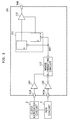
- Fig. 1 shows a circuit diagram which indicates a configuration of an electronic circuit according to an embodiment of the present disclosure.
- a clock generator circuit 2 and a power-on reset circuit 3 are connected to an IC chip 1.
- a clock signal CLK is inputted from the clock generator circuit 2 to a CLK terminal of the IC chip 1
- a power-on reset signal POR is inputted from the power-on reset circuit 3 to a POR terminal of the IC chip 1.
- An output terminal TAR of the IC chip 1 is connected to an unshown circuit or device.
- the IC chip 1 includes a digital circuit 11, an output buffer 12, a noise eliminating circuit 13, input buffers 14 and 15, and an early-initialization circuit 16.
- the digital circuit 11 is a sequential logic circuit which includes flip-flops 21 and 22. It should be noted that the digital circuit 11 may include elements other than the flip-flops 21 and 22, but they are not shown in Fig. 1 .
- the noise eliminating circuit 13 Into the noise eliminating circuit 13, the clock signal CLK is supplied via an input buffer 14, and the power-on reset signal POR is supplied via an input buffer 15; and an output signal thereof in which noise has been eliminated (a reset signal RST) is used for an asynchronous reset of the digital circuit 11.
- the noise eliminating circuit 13 delays the power-on reset signal by a predetermined number of clocks, eliminates noise in the power-on reset signal by performing a logical operation between the delayed power-on reset signal and the current power-on reset signal, and outputs a signal obtained by the logical operation as the reset signal RST to the digital circuit 11. Therefore, a period in which a reset status remains due to the power-on reset signal is set longer than the delay at the noise eliminating circuit 13.
- the early-initialization circuit 16 is put between the digital circuit 11 and the output buffer 12 connected to the output terminal TAR, fixes an output signal of the digital circuit 11 at a predetermined value until a reset status due to the power-on reset signal is released, and directly supplies an output signal of the digital circuit 11 to the output buffer 12 after the reset status due to the power-on reset signal is released.
- the digital circuit 11 outputs two output signals from the flip-flops 21 and 22.
- the early-initialization circuit 16 includes two OR operation circuits 31 and 32, performs logical operations between the respective output signals of the digital circuit 11 and the power-on reset signal, and outputs results of the logical operations.
- the value of the power-on reset signal changes to the H (high) level after the reset status is released, and this power-on reset signal is inverted and inputted as respective ones of input signals to the OR operation circuits 31 and 32.
- both of the other input and the output of the OR operation circuit 31 are set as either inverse ones or non-inverse ones
- both of the other input and the output of the OR operation circuit 32 are set as either inverse ones or non-inverse ones.
- AND operation circuits may be used instead of the OR operation circuits 31 and 32. If the AND operation circuits are used, two inputs and one output of the AND operation circuits are properly set as either inverse ones or non-inverse ones.
- the output buffer 12 is a tristate buffer. Into the output buffer 12, an input signal is supplied from the OR operation circuit 31, and a control signal is supplied from the OR operation circuit 32.
- Fig. 2 shows a timing chart which indicates an example of a clock signal, a power-on reset signal, and a status of an output terminal in the electronic circuit shown in Fig. 1 .
- the clock generator circuit 2 starts outputting the clock signal CLK with a delay from the power-on (the time To).
- the power-on reset circuit 3 releases a reset status set by a power-on reset signal POR .
- the reset status is released by changing the power-on reset signal POR from the L (low) level to the H (high) level.
- the clock signal CLK and the power-on reset signal POR are supplied to the noise eliminating circuit 13 of the IC chip 1.
- the noise eliminating circuit 13 delays the power-on reset signal by a predetermined number of clocks in the clock signal CLK, and supplies a reset signal RST (here, an L-level pulse signal) when both of the current power-on reset signal and the delayed power-on reset signal take the L level.
- a reset signal RST here, an L-level pulse signal
- the value of the output signal of the digital circuit 11 is invalid (indefinite).
- the digital circuit 11 is initialized, and afterward, the value of the output signal of the digital circuit 11 is valid.
- the power-on reset signal takes the L level during the period from the time To to the time T1 (i.e. the period when the output of the digital circuit 11 is indefinite)
- the fixed values outputted from the early-initialization circuit 16 are supplied to the output buffer 12, and a signal with the level specified by the early-initialization circuit 16 is supplied from the output buffer 12 to the output terminal TAR. Therefore, the level of the output terminal TAR is valid during the period from the time To to the time T1.
- the power supply still takes a low voltage, and therefore, does not ensure that the input buffer 15, the early-initialization circuit 16, and the output buffer 12 operate properly, and consequently, the level of the output terminal TAR is not valid.
- the power-on reset signal takes the H level, and therefore, the early-initialization circuit 16 directly supplies the output signal of the digital circuit 11 to the output buffer 12, and consequently, a signal with the level specified by the digital circuit 11 is applied to the output terminal TAR. During this period, the level of the output terminal TAR is also valid.
- the noise eliminating circuit 13 eliminates noise in the power-on reset signal and outputs a signal obtained by eliminating noise in the power-on reset signal; the digital circuit 11 is reset by the signal outputted from the noise eliminating circuit 13; and the early-initialization circuit 16 fixes an output signal of the digital circuit 11 at a predetermined value until a reset status due to the power-on reset signal is released.
- the output signal of the digital circuit 11 does not take an invalid value during a period until the reset status due to the power-on reset signal is released, and consequently, it reduces malfunction due to the reset during an initialization of the digital circuit 11.
- a forced reset signal generated in correspondence with a user's reset operation or the like may be used instead of the power-on reset signal. If the forced reset signal is used, a forced reset circuit which generates the forced reset signal is used instead of the power-on reset circuit 3.
- the signal inputted to the output buffer 12 connected to the output terminal TAR is made valid in an early time.
- a control signal inputted to an input buffer (e.g. tristate buffer) connected to the input terminal may be made valid in an early time.
- a signal inputted to an input/output buffer connected to the output terminal TAR may be made valid in an early time.
Landscapes
- Physics & Mathematics (AREA)
- Nonlinear Science (AREA)
- Electronic Switches (AREA)
- Logic Circuits (AREA)
- Manipulation Of Pulses (AREA)
Description
- The present disclosure relates to electronic circuits.
-
US 2006/103436 A1 discloses a reset control circuit and a reset control method used in a circuit system including a clock synchronous circuit, capable of resetting appropriately, especially in case of abnormality, when a clock signal is stopped or its period is longer as compared with a reset response required for detecting an abnormal state. A reset control circuit for output control of a reset signal RS is depending on a reset request signal RR and comprises a clock transforming unit for transforming and issuing a clock signal CK, while generating a clock output signal RC at delay of clock output waiting period DC is depending on the reset request signal RR, and a reset signal generator for generating a reset signal RS at delay of reset output waiting period D depending on the clock output signal RC. Further,US 2006/103436 A1 discloses that the reset control circuit comprises a reset request delay unit composed of a delay circuit and two-input OR circuit, a reset request hold unit composed of flip-flop and a logical sum operation unit composed of two-input AND circuit. - From
US 5 629 642 is known a power supply monitor which outputs a reset signal when the power supply voltage decreases, a first voltage is generated by a first voltage generator in proportion to a power supply voltage and a comparator is supplying a first signal when the first voltage becomes lower than a reference voltage. On the other hand, a slewing rate detector supplies a second signal when a slewing rate of decreasing in power supply voltage is larger than a threshold value. Then, a signal generator supplying a signal set by a trailing edge of the second signal received from the slewing rate detector except a period after the second signal is received and reset by a trailing edge of the first signal received from the comparator. Even if the power supply voltage decreases, the monitor does not generate a reset signal when the decrease in the power supply voltage is instantaneous. -
US 2006/214650 A1 discloses a semiconductor integrated circuit device incorporated in an electronic appliance provided with a control portion such as a microcomputer so as to monitor a power supply voltage to be fed to the electronic appliance and detect a set voltage, 1 and a power supply voltage monitor system system employing the same. Further,US 2006/214650 A1 discloses a semiconductor integrated circuit device provided with a delay circuit that delays an output signal when the power supply voltage is detected exceeding the set voltage. - In general, a power-on reset is used to initialize a digital circuit in an electronic device when it is powered on. In the power-on reset, for example, when the electronic device is powered on, the electronic device is initialized by supplying a reset signal to the digital circuit with a delay from the time when it is powered on.
-
Fig. 3 shows a circuit diagram which indicates an example of an electronic circuit in which a digital circuit is asynchronously reset by a power-on reset.Fig. 4 shows a timing chart which indicates an example of a clock signal, a power-on reset signal, and a status of an output terminal in the electronic circuit shown inFig. 3 . - In the electronic circuit shown in
Fig. 3 , aclock generator circuit 2 and a power-onreset circuit 3 are connected to an IC (Integrated Circuit)chip 101. A clock signal CLK is inputted from theclock generator circuit 2 to a CLK terminal of theIC chip 101, and a power-on reset signal POR is inputted from the power-onreset circuit 3 to a POR terminal of theIC chip 101. - The
IC chip 101 includes adigital circuit 111, and, an output signal of thedigital circuit 111 is applied to an output terminal TAR via anoutput buffer 112. - In a noiseful environment, if this power-on reset signal is directly used as a reset signal for an asynchronous reset, the
digital circuit 111 is reset by noise in error. Therefore, anoise eliminating circuit 113 eliminates noise in the power-on reset signal. - Into the
noise eliminating circuit 113, the clock signal CLK is supplied via aninput buffer 114, and the power-on reset signal POR is supplied via aninput buffer 115; and an output signal thereof in which noise has been eliminated (a reset signal RST) is used for an asynchronous reset of thedigital circuit 111. Thenoise eliminating circuit 113 delays the power-on reset signal by a predetermined number of clocks, eliminates noise in the power-on reset signal by performing a logical operation between the delayed power-on reset signal and the current power-on reset signal, and outputs a signal obtained by the logical operation as the reset signal RST. Therefore, even if noise occurs in the power-on reset signal, thedigital circuit 111 is not reset due to the noise. - However, in the case that the
digital circuit 111 is initialized in such way, a delay period until a reset status due to the power-on reset signal is released and the reset signal RST is supplied to the digital circuit 111 (i.e. a period from the power-on timing To to the time T1 inFig. 4 ) must be set longer than the delay at thenoise eliminating circuit 113, and consequently, during the delay period, the value of the output signal of the digital circuit is invalid (i.e. indefinite). Therefore, during this period, a circuit or device connected to the output terminal TAR may malfunction. - For instance, in the case that a control signal for a motor is outputted from the output terminal TAR, upon a power-on, during the period when the value of the output signal of the
digital circuit 111 is invalid (i.e. indefinite), the control signal may take an unexpected value and the motor runs unexpectedly. - An electronic circuit according to an aspect of the present disclosure includes a noise eliminating circuit configured to eliminate noise in a reset signal and output a signal obtained by eliminating the noise in the reset signal; a digital circuit configured to be reset by the signal outputted from the noise eliminating circuit; and an early-initialization circuit configured to fix an output signal of the digital circuit at a predetermined value until a reset status due to the reset signal is released.
- Therefore, the output signal of the digital circuit does not take an invalid value during a period until a reset status, for example, due to a power-on reset signal is released, and consequently, it reduces malfunction due to the reset during an initialization of the digital circuit.
- These and other objects, features and advantages of the present disclosure will become more apparent upon reading of the following detailed description along with the accompanied drawings.
-
-
Fig. 1 shows a circuit diagram which indicates a configuration of an electronic circuit according to an embodiment of the present disclosure; -
Fig. 2 shows a timing chart which indicates an example of a clock signal, a power-on reset signal, and a status of an output terminal in the electronic circuit shown inFig. 1 ; -
Fig. 3 shows a circuit diagram which indicates an example of an electronic circuit in which a digital circuit is asynchronously reset by a power-on reset; and -
Fig. 4 shows a timing chart which indicates an example of a clock signal, a power-on reset signal, and a status of an output terminal in the electronic circuit shown inFig. 3 . - Hereinafter, an embodiment according to aspects of the present disclosure will be explained with reference to drawings.
-
Fig. 1 shows a circuit diagram which indicates a configuration of an electronic circuit according to an embodiment of the present disclosure. - In the electronic circuit shown in
Fig. 1 , aclock generator circuit 2 and a power-onreset circuit 3 are connected to anIC chip 1. A clock signal CLK is inputted from theclock generator circuit 2 to a CLK terminal of theIC chip 1, and a power-on reset signal POR is inputted from the power-onreset circuit 3 to a POR terminal of theIC chip 1. An output terminal TAR of theIC chip 1 is connected to an unshown circuit or device. - The
IC chip 1 includes adigital circuit 11, anoutput buffer 12, anoise eliminating circuit 13,input buffers initialization circuit 16. - The
digital circuit 11 is a sequential logic circuit which includes flip-flops 21 and 22. It should be noted that thedigital circuit 11 may include elements other than the flip-flops 21 and 22, but they are not shown inFig. 1 . - Into the
noise eliminating circuit 13, the clock signal CLK is supplied via aninput buffer 14, and the power-on reset signal POR is supplied via aninput buffer 15; and an output signal thereof in which noise has been eliminated (a reset signal RST) is used for an asynchronous reset of thedigital circuit 11. Thenoise eliminating circuit 13 delays the power-on reset signal by a predetermined number of clocks, eliminates noise in the power-on reset signal by performing a logical operation between the delayed power-on reset signal and the current power-on reset signal, and outputs a signal obtained by the logical operation as the reset signal RST to thedigital circuit 11. Therefore, a period in which a reset status remains due to the power-on reset signal is set longer than the delay at thenoise eliminating circuit 13. - The early-
initialization circuit 16 is put between thedigital circuit 11 and theoutput buffer 12 connected to the output terminal TAR, fixes an output signal of thedigital circuit 11 at a predetermined value until a reset status due to the power-on reset signal is released, and directly supplies an output signal of thedigital circuit 11 to theoutput buffer 12 after the reset status due to the power-on reset signal is released. - In this embodiment, the
digital circuit 11 outputs two output signals from the flip-flops 21 and 22. The early-initialization circuit 16 includes twoOR operation circuits digital circuit 11 and the power-on reset signal, and outputs results of the logical operations. - In this embodiment, the value of the power-on reset signal changes to the H (high) level after the reset status is released, and this power-on reset signal is inverted and inputted as respective ones of input signals to the
OR operation circuits circuits OR operation circuit 31 are set as either inverse ones or non-inverse ones, and both of the other input and the output of theOR operation circuit 32 are set as either inverse ones or non-inverse ones. - In the early-
initialization circuit 16, AND operation circuits may be used instead of theOR operation circuits - The
output buffer 12 is a tristate buffer. Into theoutput buffer 12, an input signal is supplied from theOR operation circuit 31, and a control signal is supplied from theOR operation circuit 32. - In the following part, a behavior of the aforementioned electronic circuit is explained.
-
Fig. 2 shows a timing chart which indicates an example of a clock signal, a power-on reset signal, and a status of an output terminal in the electronic circuit shown inFig. 1 . - When an electronic device which includes the present electronic circuit is powered-on (at the time To), each part starts operating in the electronic circuit.
- As shown in
Fig. 2 , theclock generator circuit 2 starts outputting the clock signal CLK with a delay from the power-on (the time To). - In addition, with a delay from the power-on (the time To), the power-on
reset circuit 3 releases a reset status set by a power-on reset signal POR . In this embodiment, the reset status is released by changing the power-on reset signal POR from the L (low) level to the H (high) level. - The clock signal CLK and the power-on reset signal POR are supplied to the
noise eliminating circuit 13 of theIC chip 1. Thenoise eliminating circuit 13 delays the power-on reset signal by a predetermined number of clocks in the clock signal CLK, and supplies a reset signal RST (here, an L-level pulse signal) when both of the current power-on reset signal and the delayed power-on reset signal take the L level. - Before the reset signal RST is supplied (i.e. in the period from the time To to the time T1), the value of the output signal of the
digital circuit 11 is invalid (indefinite). When the reset signal RST is supplied (at the time T1), thedigital circuit 11 is initialized, and afterward, the value of the output signal of thedigital circuit 11 is valid. - On the other hand, since the power-on reset signal takes the L level during the period from the time To to the time T1 (i.e. the period when the output of the
digital circuit 11 is indefinite), the fixed values outputted from the early-initialization circuit 16 are supplied to theoutput buffer 12, and a signal with the level specified by the early-initialization circuit 16 is supplied from theoutput buffer 12 to the output terminal TAR. Therefore, the level of the output terminal TAR is valid during the period from the time To to the time T1. However, in a short time immediately after the power-on, the power supply still takes a low voltage, and therefore, does not ensure that theinput buffer 15, the early-initialization circuit 16, and theoutput buffer 12 operate properly, and consequently, the level of the output terminal TAR is not valid. - During the period after the time T1, the power-on reset signal takes the H level, and therefore, the early-
initialization circuit 16 directly supplies the output signal of thedigital circuit 11 to theoutput buffer 12, and consequently, a signal with the level specified by thedigital circuit 11 is applied to the output terminal TAR. During this period, the level of the output terminal TAR is also valid. - As shown in
Fig. 2 , in the period after the time T1, if noise occurs in the power-on reset signal, the fixed values outputted from the early-initialization circuit 16 are supplied to theoutput buffer 12 due to the noise. In this time, it is not ensured that the fixed values are identical to proper values of the output signals of thedigital circuit 11, and therefore, the level of the output terminal TAR is not valid in the period when the noise occurs in the power-on reset signal. However, since this noise is eliminated by thenoise eliminating circuit 13, the noise does not result in supplying the reset signal RST to thedigital circuit 11, and thedigital circuit 11 continues to operate properly. Since thedigital circuit 11 continues to operate properly, the level of the output terminal TAR returns to be valid immediately after the noise in the power-on reset signal disappears. - In the aforementioned embodiment, the
noise eliminating circuit 13 eliminates noise in the power-on reset signal and outputs a signal obtained by eliminating noise in the power-on reset signal; thedigital circuit 11 is reset by the signal outputted from thenoise eliminating circuit 13; and the early-initialization circuit 16 fixes an output signal of thedigital circuit 11 at a predetermined value until a reset status due to the power-on reset signal is released. - Therefore, the output signal of the
digital circuit 11 does not take an invalid value during a period until the reset status due to the power-on reset signal is released, and consequently, it reduces malfunction due to the reset during an initialization of thedigital circuit 11. - The description of the present disclosure has been presented for purposes of illustration and description, and is not intended to be exhaustive or limited to the disclosure in the form disclosed.
- For example, in the aforementioned embodiment, a forced reset signal generated in correspondence with a user's reset operation or the like may be used instead of the power-on reset signal. If the forced reset signal is used, a forced reset circuit which generates the forced reset signal is used instead of the power-on
reset circuit 3. - Further, in the aforementioned embodiment, the signal inputted to the
output buffer 12 connected to the output terminal TAR is made valid in an early time. In the same manner, a control signal inputted to an input buffer (e.g. tristate buffer) connected to the input terminal may be made valid in an early time. Furthermore, in the same manner, a signal inputted to an input/output buffer connected to the output terminal TAR may be made valid in an early time. - It should be understood that various changes and modifications to the embodiments described herein will be apparent to those skilled in the art. Such changes and modifications may be made without departing from the scope of the present subject matter and without diminishing its intended advantages. It is therefore intended that such changes and modifications be covered by the appended claims.
Claims (8)
- An electronic circuit, characterized by comprising:an IC chip (1) comprisinga noise eliminating circuit (13),a digital circuit (11),an early-initialization circuit (16) and further comprisingan input terminal (POR) of a power-on reset signal,an output terminal (TAR) andan output buffer (12) connected to the output terminal (TAR); whereinthe noise eliminating circuit (13) is configured to eliminate noise in a power-on reset signal and output a signal obtained by eliminating the noise in the power-on reset signal; whereinthe digital circuit (11) is configured to be reset by the signal outputted from the noise eliminating circuit (13); whereinthe early-initialization circuit (16) is connected to the output buffer (12); whereinthe early-initialization circuit (16) is arranged between the digital circuit (11) and the output buffer (12) connected to the output terminal (TAR); whereinthe early-initialization circuit (16) is configured to produce a fixed value as an output signal until a reset status set bythe power-on reset signal is released and directly supplies the output signal of the digital circuit (11) upon the power-on reset status is released; whereinthe early-initialization circuit (16) is configured to supply the fixed value to the output buffer (12) from a point of time at power-on to a point of time when the reset status set by the power-on reset signal is released and whereinthe early-initialization circuit (16) is further configured to perform a logical operation between the output signal of the digital circuit (11) and the power-on reset signal, and output a result of the logical operation.
- The electronic circuit according to claim 1, wherein
the IC chip (1) comprises an input buffer (14) to supply a clock signal from an input terminal (CLK) via the input buffer (14) to the noise eliminating circuit (13). - The electronic circuit according to claim 1 or 2, wherein
the IC chip (1) comprises an input buffer (15) to supply a power-on reset signal from the input terminal (POR) via the input buffer (15) to the noise eliminating circuit (13). - The electronic circuit according to any of claims 1 to 3, wherein
the digital circuit (11) comprises two flip-flops (21, 22) and is configured to output two output signals to the early-initialization circuit (16). - The electronic circuit according to claim 4, wherein
the early-initialization circuit (16) includes a first and a second operation circuit (31, 32), to perform the logical operations between the respective output signals of the digital circuit (11) and the power-on reset signal, and outputs results of the logical operations. - The electronic circuit according to any of claims 1 to 5, wherein
the output buffer (12) is a tristate buffer, wherein an input signal is supplied from the first operation circuit (31) and a control signal is supplied from the second operation circuit (32). - The electronic circuit according to any of claims 1 to 6, wherein:the digital circuit (11) is a sequential logic circuit, andthe noise eliminating circuit (13) is further configured to asynchronously reset the sequential logic circuit according to the signal obtained by eliminating the noise in the power-on reset signal.
- The electronic circuit according to any of claims 1 to 7, wherein:the noise eliminating circuit (13) is further configured to delay the power-on reset signal by a predetermined number of clocks, eliminate noise in the power-on reset signal by performing a logical operation between the delayed power-on reset signal and the current power-on reset signal, and output a signal obtained by the logical operation as the signal obtained by eliminating the noise in the power-on reset signal.
Applications Claiming Priority (1)
| Application Number | Priority Date | Filing Date | Title |
|---|---|---|---|
| JP2011216033A JP5501320B2 (en) | 2011-09-30 | 2011-09-30 | Electronic circuit |
Publications (2)
| Publication Number | Publication Date |
|---|---|
| EP2575256A1 EP2575256A1 (en) | 2013-04-03 |
| EP2575256B1 true EP2575256B1 (en) | 2016-01-20 |
Family
ID=47048921
Family Applications (1)
| Application Number | Title | Priority Date | Filing Date |
|---|---|---|---|
| EP12006703.8A Not-in-force EP2575256B1 (en) | 2011-09-30 | 2012-09-25 | Electronic circuit |
Country Status (4)
| Country | Link |
|---|---|
| US (1) | US8729934B2 (en) |
| EP (1) | EP2575256B1 (en) |
| JP (1) | JP5501320B2 (en) |
| CN (1) | CN103036545B (en) |
Families Citing this family (5)
| Publication number | Priority date | Publication date | Assignee | Title |
|---|---|---|---|---|
| JP5706455B2 (en) * | 2013-02-19 | 2015-04-22 | Necエンジニアリング株式会社 | Control circuit, circuit system, and control method |
| CN106301300B (en) * | 2016-08-02 | 2019-04-05 | 芯启源(上海)半导体科技有限公司 | Pulse synchronization circuit and processor with safety reset function |
| JP6661585B2 (en) | 2017-09-26 | 2020-03-11 | キヤノン株式会社 | Information processing device |
| JP7074699B2 (en) * | 2019-02-28 | 2022-05-24 | ファナック株式会社 | Glitch removal circuit and electronic equipment |
| CN113792509B (en) * | 2021-11-16 | 2022-02-18 | 苏州浪潮智能科技有限公司 | A reset signal balance method and device |
Citations (1)
| Publication number | Priority date | Publication date | Assignee | Title |
|---|---|---|---|---|
| JP2008226138A (en) * | 2007-03-15 | 2008-09-25 | Seiko Epson Corp | Information processing device |
Family Cites Families (14)
| Publication number | Priority date | Publication date | Assignee | Title |
|---|---|---|---|---|
| US4438357A (en) * | 1982-06-17 | 1984-03-20 | Baxter Travenol Laboratories, Inc. | Level sensitive reset circuit for digital logic |
| US4940904A (en) * | 1988-05-23 | 1990-07-10 | Industrial Technology Research Institute | Output circuit for producing positive and negative pulses at a single output terminal |
| JPH07161157A (en) * | 1993-12-07 | 1995-06-23 | Matsushita Electric Ind Co Ltd | Magnetic recording / reproducing device |
| JPH0954620A (en) | 1995-08-18 | 1997-02-25 | Mitsubishi Electric Corp | Power supply monitoring circuit |
| DE19534785C1 (en) * | 1995-09-19 | 1997-01-16 | Siemens Ag | Circuit arrangement for generating an enable signal for a clock-controllable circuit |
| JP3647302B2 (en) | 1999-03-18 | 2005-05-11 | 富士通株式会社 | Power-on reset circuit and integrated circuit device having the same |
| US6690220B2 (en) * | 2000-06-30 | 2004-02-10 | Matsushita Electric Industrial Co., Ltd. | Reset circuit of semiconductor circuit |
| JP2003223241A (en) * | 2002-01-31 | 2003-08-08 | Mitsubishi Electric Corp | Reset control device |
| JP2004320400A (en) * | 2003-04-16 | 2004-11-11 | Daikin Ind Ltd | Semiconductor integrated circuit |
| JP4127283B2 (en) * | 2003-04-25 | 2008-07-30 | 日本電気株式会社 | Reset circuit and digital communication device |
| WO2005020437A1 (en) * | 2003-08-22 | 2005-03-03 | Rohm Co., Ltd | Semiconductor integrated circuit device and power supply voltage monitor system employing it |
| JP4437541B2 (en) | 2004-11-17 | 2010-03-24 | 富士通マイクロエレクトロニクス株式会社 | Reset control circuit and reset control method |
| JP2007088712A (en) * | 2005-09-21 | 2007-04-05 | Seiko Instruments Inc | Noise filter circuit |
| US8258844B2 (en) * | 2006-08-03 | 2012-09-04 | Seagate Technology Llc | System-wide reset of multiple electronic devices |
-
2011
- 2011-09-30 JP JP2011216033A patent/JP5501320B2/en active Active
-
2012
- 2012-09-21 US US13/624,538 patent/US8729934B2/en active Active
- 2012-09-25 EP EP12006703.8A patent/EP2575256B1/en not_active Not-in-force
- 2012-10-08 CN CN201210391112.5A patent/CN103036545B/en not_active Expired - Fee Related
Patent Citations (1)
| Publication number | Priority date | Publication date | Assignee | Title |
|---|---|---|---|---|
| JP2008226138A (en) * | 2007-03-15 | 2008-09-25 | Seiko Epson Corp | Information processing device |
Also Published As
| Publication number | Publication date |
|---|---|
| US8729934B2 (en) | 2014-05-20 |
| CN103036545B (en) | 2016-01-13 |
| CN103036545A (en) | 2013-04-10 |
| EP2575256A1 (en) | 2013-04-03 |
| JP5501320B2 (en) | 2014-05-21 |
| US20130082750A1 (en) | 2013-04-04 |
| JP2013077939A (en) | 2013-04-25 |
Similar Documents
| Publication | Publication Date | Title |
|---|---|---|
| EP2575256B1 (en) | Electronic circuit | |
| US9436647B2 (en) | IIC bus start-stop detection circuit | |
| CN101135921A (en) | Multi-clock switching device and switching method thereof | |
| US20190356313A1 (en) | Reducing glitches that occur when multiplexing of asynchronous clocks using flip-flops and logic gates | |
| EP1237282B1 (en) | Circuit for the detection of clock signal period abnormalities | |
| US8473797B2 (en) | Circuits and methods for clock malfunction detection | |
| US7882279B2 (en) | Bidirectional control circuit | |
| US9171596B2 (en) | Short asynchronous glitch | |
| CN116054798B (en) | A method and device for eliminating sequential metastable state in power-on and power-off reset of multiple voltage domains | |
| JP4007027B2 (en) | Power-on reset circuit | |
| JP5125605B2 (en) | Integrated circuit device having reset control | |
| US9218030B2 (en) | Programming interface and method | |
| US20180131375A1 (en) | Communication between integrated circuits | |
| JP2000261310A (en) | Asynchronous signal synchronization circuit and semiconductor integrated circuit | |
| EP3428768B1 (en) | Robust boot block design and architecture | |
| JPH10200586A (en) | Data signal transmission method and signal input circuit for semiconductor device | |
| JP4279023B2 (en) | Status display information setting circuit | |
| JP4122128B2 (en) | Edge detection circuit | |
| CN101324654A (en) | Semiconductor integrated device | |
| KR100266627B1 (en) | Power down circuit | |
| JP2010003199A (en) | Semiconductor integrated circuit device | |
| JPH1028383A (en) | PWM signal generator | |
| KR101145113B1 (en) | Reset circuit for controller and reset method using the same | |
| JP4934980B2 (en) | Bus receiver circuit and noise removing method used for the bus receiver circuit | |
| CN119994819A (en) | A self-recovery method and circuit for chip ESD protection system |
Legal Events
| Date | Code | Title | Description |
|---|---|---|---|
| PUAI | Public reference made under article 153(3) epc to a published international application that has entered the european phase |
Free format text: ORIGINAL CODE: 0009012 |
|
| AK | Designated contracting states |
Kind code of ref document: A1 Designated state(s): AL AT BE BG CH CY CZ DE DK EE ES FI FR GB GR HR HU IE IS IT LI LT LU LV MC MK MT NL NO PL PT RO RS SE SI SK SM TR |
|
| AX | Request for extension of the european patent |
Extension state: BA ME |
|
| 17P | Request for examination filed |
Effective date: 20130916 |
|
| RBV | Designated contracting states (corrected) |
Designated state(s): AL AT BE BG CH CY CZ DE DK EE ES FI FR GB GR HR HU IE IS IT LI LT LU LV MC MK MT NL NO PL PT RO RS SE SI SK SM TR |
|
| 17Q | First examination report despatched |
Effective date: 20131217 |
|
| GRAP | Despatch of communication of intention to grant a patent |
Free format text: ORIGINAL CODE: EPIDOSNIGR1 |
|
| RIC1 | Information provided on ipc code assigned before grant |
Ipc: H03K 5/1252 20060101ALN20150617BHEP Ipc: H03K 17/22 20060101AFI20150617BHEP |
|
| INTG | Intention to grant announced |
Effective date: 20150722 |
|
| GRAS | Grant fee paid |
Free format text: ORIGINAL CODE: EPIDOSNIGR3 |
|
| GRAA | (expected) grant |
Free format text: ORIGINAL CODE: 0009210 |
|
| AK | Designated contracting states |
Kind code of ref document: B1 Designated state(s): AL AT BE BG CH CY CZ DE DK EE ES FI FR GB GR HR HU IE IS IT LI LT LU LV MC MK MT NL NO PL PT RO RS SE SI SK SM TR |
|
| REG | Reference to a national code |
Ref country code: GB Ref legal event code: FG4D |
|
| REG | Reference to a national code |
Ref country code: CH Ref legal event code: EP |
|
| REG | Reference to a national code |
Ref country code: IE Ref legal event code: FG4D |
|
| REG | Reference to a national code |
Ref country code: AT Ref legal event code: REF Ref document number: 772134 Country of ref document: AT Kind code of ref document: T Effective date: 20160215 |
|
| REG | Reference to a national code |
Ref country code: DE Ref legal event code: R082 Ref document number: 602012014027 Country of ref document: DE Representative=s name: SCHAEFER PATENT- UND RECHTSANWAELTE, DE |
|
| REG | Reference to a national code |
Ref country code: DE Ref legal event code: R096 Ref document number: 602012014027 Country of ref document: DE |
|
| REG | Reference to a national code |
Ref country code: LT Ref legal event code: MG4D Ref country code: NL Ref legal event code: MP Effective date: 20160120 |
|
| REG | Reference to a national code |
Ref country code: AT Ref legal event code: MK05 Ref document number: 772134 Country of ref document: AT Kind code of ref document: T Effective date: 20160120 |
|
| PG25 | Lapsed in a contracting state [announced via postgrant information from national office to epo] |
Ref country code: NL Free format text: LAPSE BECAUSE OF FAILURE TO SUBMIT A TRANSLATION OF THE DESCRIPTION OR TO PAY THE FEE WITHIN THE PRESCRIBED TIME-LIMIT Effective date: 20160120 |
|
| PG25 | Lapsed in a contracting state [announced via postgrant information from national office to epo] |
Ref country code: HR Free format text: LAPSE BECAUSE OF FAILURE TO SUBMIT A TRANSLATION OF THE DESCRIPTION OR TO PAY THE FEE WITHIN THE PRESCRIBED TIME-LIMIT Effective date: 20160120 Ref country code: IT Free format text: LAPSE BECAUSE OF FAILURE TO SUBMIT A TRANSLATION OF THE DESCRIPTION OR TO PAY THE FEE WITHIN THE PRESCRIBED TIME-LIMIT Effective date: 20160120 Ref country code: NO Free format text: LAPSE BECAUSE OF FAILURE TO SUBMIT A TRANSLATION OF THE DESCRIPTION OR TO PAY THE FEE WITHIN THE PRESCRIBED TIME-LIMIT Effective date: 20160420 Ref country code: ES Free format text: LAPSE BECAUSE OF FAILURE TO SUBMIT A TRANSLATION OF THE DESCRIPTION OR TO PAY THE FEE WITHIN THE PRESCRIBED TIME-LIMIT Effective date: 20160120 Ref country code: GR Free format text: LAPSE BECAUSE OF FAILURE TO SUBMIT A TRANSLATION OF THE DESCRIPTION OR TO PAY THE FEE WITHIN THE PRESCRIBED TIME-LIMIT Effective date: 20160421 Ref country code: FI Free format text: LAPSE BECAUSE OF FAILURE TO SUBMIT A TRANSLATION OF THE DESCRIPTION OR TO PAY THE FEE WITHIN THE PRESCRIBED TIME-LIMIT Effective date: 20160120 |
|
| REG | Reference to a national code |
Ref country code: FR Ref legal event code: PLFP Year of fee payment: 5 |
|
| PG25 | Lapsed in a contracting state [announced via postgrant information from national office to epo] |
Ref country code: PT Free format text: LAPSE BECAUSE OF FAILURE TO SUBMIT A TRANSLATION OF THE DESCRIPTION OR TO PAY THE FEE WITHIN THE PRESCRIBED TIME-LIMIT Effective date: 20160520 Ref country code: SE Free format text: LAPSE BECAUSE OF FAILURE TO SUBMIT A TRANSLATION OF THE DESCRIPTION OR TO PAY THE FEE WITHIN THE PRESCRIBED TIME-LIMIT Effective date: 20160120 Ref country code: LT Free format text: LAPSE BECAUSE OF FAILURE TO SUBMIT A TRANSLATION OF THE DESCRIPTION OR TO PAY THE FEE WITHIN THE PRESCRIBED TIME-LIMIT Effective date: 20160120 Ref country code: PL Free format text: LAPSE BECAUSE OF FAILURE TO SUBMIT A TRANSLATION OF THE DESCRIPTION OR TO PAY THE FEE WITHIN THE PRESCRIBED TIME-LIMIT Effective date: 20160120 Ref country code: RS Free format text: LAPSE BECAUSE OF FAILURE TO SUBMIT A TRANSLATION OF THE DESCRIPTION OR TO PAY THE FEE WITHIN THE PRESCRIBED TIME-LIMIT Effective date: 20160120 Ref country code: IS Free format text: LAPSE BECAUSE OF FAILURE TO SUBMIT A TRANSLATION OF THE DESCRIPTION OR TO PAY THE FEE WITHIN THE PRESCRIBED TIME-LIMIT Effective date: 20160520 Ref country code: LV Free format text: LAPSE BECAUSE OF FAILURE TO SUBMIT A TRANSLATION OF THE DESCRIPTION OR TO PAY THE FEE WITHIN THE PRESCRIBED TIME-LIMIT Effective date: 20160120 Ref country code: AT Free format text: LAPSE BECAUSE OF FAILURE TO SUBMIT A TRANSLATION OF THE DESCRIPTION OR TO PAY THE FEE WITHIN THE PRESCRIBED TIME-LIMIT Effective date: 20160120 |
|
| REG | Reference to a national code |
Ref country code: DE Ref legal event code: R097 Ref document number: 602012014027 Country of ref document: DE |
|
| PG25 | Lapsed in a contracting state [announced via postgrant information from national office to epo] |
Ref country code: DK Free format text: LAPSE BECAUSE OF FAILURE TO SUBMIT A TRANSLATION OF THE DESCRIPTION OR TO PAY THE FEE WITHIN THE PRESCRIBED TIME-LIMIT Effective date: 20160120 Ref country code: EE Free format text: LAPSE BECAUSE OF FAILURE TO SUBMIT A TRANSLATION OF THE DESCRIPTION OR TO PAY THE FEE WITHIN THE PRESCRIBED TIME-LIMIT Effective date: 20160120 |
|
| PLBE | No opposition filed within time limit |
Free format text: ORIGINAL CODE: 0009261 |
|
| STAA | Information on the status of an ep patent application or granted ep patent |
Free format text: STATUS: NO OPPOSITION FILED WITHIN TIME LIMIT |
|
| PG25 | Lapsed in a contracting state [announced via postgrant information from national office to epo] |
Ref country code: SK Free format text: LAPSE BECAUSE OF FAILURE TO SUBMIT A TRANSLATION OF THE DESCRIPTION OR TO PAY THE FEE WITHIN THE PRESCRIBED TIME-LIMIT Effective date: 20160120 Ref country code: RO Free format text: LAPSE BECAUSE OF FAILURE TO SUBMIT A TRANSLATION OF THE DESCRIPTION OR TO PAY THE FEE WITHIN THE PRESCRIBED TIME-LIMIT Effective date: 20160120 Ref country code: SM Free format text: LAPSE BECAUSE OF FAILURE TO SUBMIT A TRANSLATION OF THE DESCRIPTION OR TO PAY THE FEE WITHIN THE PRESCRIBED TIME-LIMIT Effective date: 20160120 Ref country code: CZ Free format text: LAPSE BECAUSE OF FAILURE TO SUBMIT A TRANSLATION OF THE DESCRIPTION OR TO PAY THE FEE WITHIN THE PRESCRIBED TIME-LIMIT Effective date: 20160120 |
|
| 26N | No opposition filed |
Effective date: 20161021 |
|
| PG25 | Lapsed in a contracting state [announced via postgrant information from national office to epo] |
Ref country code: BE Free format text: LAPSE BECAUSE OF FAILURE TO SUBMIT A TRANSLATION OF THE DESCRIPTION OR TO PAY THE FEE WITHIN THE PRESCRIBED TIME-LIMIT Effective date: 20160120 |
|
| PG25 | Lapsed in a contracting state [announced via postgrant information from national office to epo] |
Ref country code: BG Free format text: LAPSE BECAUSE OF FAILURE TO SUBMIT A TRANSLATION OF THE DESCRIPTION OR TO PAY THE FEE WITHIN THE PRESCRIBED TIME-LIMIT Effective date: 20160420 Ref country code: SI Free format text: LAPSE BECAUSE OF FAILURE TO SUBMIT A TRANSLATION OF THE DESCRIPTION OR TO PAY THE FEE WITHIN THE PRESCRIBED TIME-LIMIT Effective date: 20160120 |
|
| PG25 | Lapsed in a contracting state [announced via postgrant information from national office to epo] |
Ref country code: MC Free format text: LAPSE BECAUSE OF FAILURE TO SUBMIT A TRANSLATION OF THE DESCRIPTION OR TO PAY THE FEE WITHIN THE PRESCRIBED TIME-LIMIT Effective date: 20160120 |
|
| REG | Reference to a national code |
Ref country code: CH Ref legal event code: PL |
|
| REG | Reference to a national code |
Ref country code: IE Ref legal event code: MM4A |
|
| PG25 | Lapsed in a contracting state [announced via postgrant information from national office to epo] |
Ref country code: LI Free format text: LAPSE BECAUSE OF NON-PAYMENT OF DUE FEES Effective date: 20160930 Ref country code: IE Free format text: LAPSE BECAUSE OF NON-PAYMENT OF DUE FEES Effective date: 20160925 Ref country code: CH Free format text: LAPSE BECAUSE OF NON-PAYMENT OF DUE FEES Effective date: 20160930 |
|
| REG | Reference to a national code |
Ref country code: FR Ref legal event code: PLFP Year of fee payment: 6 |
|
| PG25 | Lapsed in a contracting state [announced via postgrant information from national office to epo] |
Ref country code: LU Free format text: LAPSE BECAUSE OF NON-PAYMENT OF DUE FEES Effective date: 20160925 |
|
| PG25 | Lapsed in a contracting state [announced via postgrant information from national office to epo] |
Ref country code: CY Free format text: LAPSE BECAUSE OF FAILURE TO SUBMIT A TRANSLATION OF THE DESCRIPTION OR TO PAY THE FEE WITHIN THE PRESCRIBED TIME-LIMIT Effective date: 20160120 Ref country code: HU Free format text: LAPSE BECAUSE OF FAILURE TO SUBMIT A TRANSLATION OF THE DESCRIPTION OR TO PAY THE FEE WITHIN THE PRESCRIBED TIME-LIMIT; INVALID AB INITIO Effective date: 20120925 |
|
| PG25 | Lapsed in a contracting state [announced via postgrant information from national office to epo] |
Ref country code: TR Free format text: LAPSE BECAUSE OF FAILURE TO SUBMIT A TRANSLATION OF THE DESCRIPTION OR TO PAY THE FEE WITHIN THE PRESCRIBED TIME-LIMIT Effective date: 20160120 Ref country code: MK Free format text: LAPSE BECAUSE OF FAILURE TO SUBMIT A TRANSLATION OF THE DESCRIPTION OR TO PAY THE FEE WITHIN THE PRESCRIBED TIME-LIMIT Effective date: 20160120 Ref country code: MT Free format text: LAPSE BECAUSE OF NON-PAYMENT OF DUE FEES Effective date: 20160930 |
|
| REG | Reference to a national code |
Ref country code: FR Ref legal event code: PLFP Year of fee payment: 7 |
|
| PG25 | Lapsed in a contracting state [announced via postgrant information from national office to epo] |
Ref country code: AL Free format text: LAPSE BECAUSE OF FAILURE TO SUBMIT A TRANSLATION OF THE DESCRIPTION OR TO PAY THE FEE WITHIN THE PRESCRIBED TIME-LIMIT Effective date: 20160120 |
|
| P01 | Opt-out of the competence of the unified patent court (upc) registered |
Effective date: 20230420 |
|
| PGFP | Annual fee paid to national office [announced via postgrant information from national office to epo] |
Ref country code: GB Payment date: 20230823 Year of fee payment: 12 |
|
| PGFP | Annual fee paid to national office [announced via postgrant information from national office to epo] |
Ref country code: FR Payment date: 20230822 Year of fee payment: 12 Ref country code: DE Payment date: 20230822 Year of fee payment: 12 |
|
| REG | Reference to a national code |
Ref country code: DE Ref legal event code: R119 Ref document number: 602012014027 Country of ref document: DE |
|
| GBPC | Gb: european patent ceased through non-payment of renewal fee |
Effective date: 20240925 |
|
| PG25 | Lapsed in a contracting state [announced via postgrant information from national office to epo] |
Ref country code: DE Free format text: LAPSE BECAUSE OF NON-PAYMENT OF DUE FEES Effective date: 20250401 |
|
| PG25 | Lapsed in a contracting state [announced via postgrant information from national office to epo] |
Ref country code: GB Free format text: LAPSE BECAUSE OF NON-PAYMENT OF DUE FEES Effective date: 20240925 |
|
| PG25 | Lapsed in a contracting state [announced via postgrant information from national office to epo] |
Ref country code: FR Free format text: LAPSE BECAUSE OF NON-PAYMENT OF DUE FEES Effective date: 20240930 |