EP2575254A1 - Configurable spread spectrum oscillator - Google Patents
Configurable spread spectrum oscillator Download PDFInfo
- Publication number
- EP2575254A1 EP2575254A1 EP12186567A EP12186567A EP2575254A1 EP 2575254 A1 EP2575254 A1 EP 2575254A1 EP 12186567 A EP12186567 A EP 12186567A EP 12186567 A EP12186567 A EP 12186567A EP 2575254 A1 EP2575254 A1 EP 2575254A1
- Authority
- EP
- European Patent Office
- Prior art keywords
- spread spectrum
- oscillator
- inverter
- duty cycle
- oscillator circuit
- Prior art date
- Legal status (The legal status is an assumption and is not a legal conclusion. Google has not performed a legal analysis and makes no representation as to the accuracy of the status listed.)
- Granted
Links
Images


Classifications
-
- H—ELECTRICITY
- H03—ELECTRONIC CIRCUITRY
- H03K—PULSE TECHNIQUE
- H03K3/00—Circuits for generating electric pulses; Monostable, bistable or multistable circuits
- H03K3/84—Generating pulses having a predetermined statistical distribution of a parameter, e.g. random pulse generators
-
- H—ELECTRICITY
- H03—ELECTRONIC CIRCUITRY
- H03K—PULSE TECHNIQUE
- H03K7/00—Modulating pulses with a continuously-variable modulating signal
- H03K7/08—Duration or width modulation ; Duty cycle modulation
Definitions
- the present invention is directed to oscillators, and more particularly, exemplary embodiments of the present invention are directed to configurable spread spectrum oscillators.
- Oscillators may be used in power supplies to achieve a plurality of functionality, for example, sinusoidal or time-varying output.
- Spread spectrum oscillators produce a frequency sweep of time-varying outputs which may be very useful in reducing electromagnetic interference in power supplies as well as for providing additional functionality.
- a spread spectrum oscillator includes a high frequency oscillator circuit configured to oscillate at a first frequency, and a low frequency oscillator circuit configured to oscillate at a second frequency and resistively coupled to a current summing node of the high frequency oscillator circuit.
- the first frequency is higher than the second frequency.
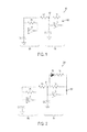
- FIG. 1 is a diagram of a spread spectrum oscillator, according to an exemplary embodiment
- FIG. 2 is a diagram of a spread spectrum oscillator with fixed duty cycle adjustability, according to an exemplary embodiment
- FIG. 3 is a diagram of a spread spectrum oscillator with adjustable duty cycle adjustability, according to an exemplary embodiment
- FIG. 4 is a diagram of a spread spectrum oscillator with stabilized hysteresis, according to an exemplary embodiment.
- FIG. 5 is a diagram of a spread spectrum oscillator including a plurality of configuration options, according to an exemplary embodiment.
- spread spectrum oscillators include complex components that are difficult to implement in a variety of applications.
- one or more of the embodiments of the present invention disclosed herein may provide a spread spectrum oscillator which is both low in cost and highly configurable.
- the technical effects and benefits of the present invention include greater adaptability and easier integration in power supplies.
- the oscillator 100 includes a first resistor R1, a first inverter I1, and a first capacitor C1 arranged as a low frequency oscillator circuit 110.
- the first inverter I1 may be a non-linear trigger inverter, such as a Schmitt trigger Inverter, to promote a non-sinusoidal triangle-like waveform at a low frequency.
- the first capacitor C1 may actively couple the input of the first inverter I1 to ground.
- the actual values of the resistor R1 and capacitor C1 may be chosen to promote low frequency oscillation of the circuit 110 as will be understood by one of ordinary skill the art.
- the oscillator 100 further includes a second resistor R3, a second inverter I2, and a second capacitor C2 arranged as a high frequency oscillator circuit 111.
- the second inverter 12 may be a non-linear trigger inverter, such as a Schmitt trigger Inverter, to promote a non-sinusoidal triangle-like waveform.
- the frequency of the non-sinusoidal triangle-like waveform produced by the second inverter I2 is at a frequency higher than that produced by the low frequency oscillator circuit 110.
- the second capacitor C2 may actively couple the input of the second inverter I2 to ground.
- the actual values of the resistor R3 and capacitor C2 may be chosen to promote high frequency oscillation of the circuit 111.
- the high frequency oscillator circuit 111 may be configured to oscillate at a first frequency and the low frequency oscillator circuit 110 may be configured to oscillate at a second frequency which is lower than the first frequency.
- the oscillator further includes a third resistor R2 coupled between respective current summing nodes of the circuits 110 and 111.
- the actual value of resistor R2 varies an amount of current seen at node 101 of the circuit 111.
- the circuit 110 is arranged to produce a non-sinusoidal triangle-like waveform at a relatively low frequency, when the value of the waveform increases and decreases, the frequency of oscillation at circuit 111 increases and decreases or "sweeps.”
- the particular arrangement illustrated in FIG. 1 forms a spread spectrum oscillator outputting a time-varying and frequency-varying waveform at node 102.
- the particular arrangement of the high frequency oscillator circuit 111 and low frequency oscillator circuit 110 may be altered without departing from the spirit and scope of exemplary embodiments of the present invention.
- the associated frequencies of circuits 110 and 111 may be reversed or "flipped" while still providing for spread spectrum oscillation at node 102 (e.g., such that oscillator circuit 111 oscillates at a lower frequency than oscillator circuit 110).
- the frequency of oscillation, rate of change in frequency, and size of the frequency spectrum swept may be configurable through selection of any desired values for ratios between the resistors and capacitors illustrated.
- resistor R1 and capacitor C1 control the frequency of the circuit 110 and thus also the rate of change in frequency of the output node 102
- resistor R3 and capacitor C2 control the base oscillation frequency of circuit 111
- resistor R2 controls the size of the spectrum swept at node 102.
- many more aspects of a spread spectrum oscillator may be controlled and configured through the addition of relatively simple electronic components.
- FIG. 2 is a diagram of a spread spectrum oscillator with fixed duty cycle adjustability, according to an exemplary embodiment.
- the oscillator 200 is substantially similar to the oscillator 100, with the addition of the diode D1 and the resistor R4.
- the diode D1 and resistor R4 are electrically in series with one another and connected between the current summing node 101 and the output node 102.
- the diode D1 in combination with resistor R4 alters the duty cycle of the waveform at the node 102 because of the switching nature of the diode D1, which serves to change an amount of current flowing during charge and discharge cycles of the capacitors illustrated, thereby adjusting the duty cycle seen at output node 102.
- the varying degree of duty cycle change is caused by selection of the size of resistor R4 and breakdown voltage of the diode D1. Furthermore, a direction of the p-n junction of the diode D1 determines which half of the duty cycle is adjusted, and may therefore be changed from one direction to another to adjust duty cycle.
- the oscillator 200 includes a fixed duty cycle adjustability.
- FIG. 3 is a diagram of a spread spectrum oscillator with continually adjustable duty cycle adjustability, according to an exemplary embodiment.
- the oscillator 300 is substantially similar to the oscillator 100, with the addition of the resistor R5 and duty cycle adjust node 103.
- a positive voltage applied at node 103 increases an overall duty cycle of a waveform seen at node 102.
- a negative voltage at node 103 decreases an overall duty cycle of a waveform seen at node 102.
- different control voltages may be applied at node 103 for continual adjustment.
- feedback from a line voltage of a power supply in communication with the oscillator 300 may be applied for adjusting and trimming a duty cycle at node 103.
- FIG. 4 is a diagram of a spread spectrum oscillator with stabilized hysteresis, according to an exemplary embodiment.
- the oscillator 400 includes stabilized hysteresis through the addition of additional inverters I3 and I4 and capacitors C3 and C4 arranged in series across respective output and summing nodes of the circuits 110 and 111.
- the arrangement of oscillator 400 allows for capacitive voltage division which reduces part-to-part hysteresis differences across the inverters I1 and I3. Additionally, the arrangement of oscillator 400 allows for capacitive for capacitive voltage division which reduces part-to-part hysteresis differences across the inverters I2 and I4. As such, through capacitive voltage division the hysteresis differences across a plurality of parts is stabilized thereby realizing consistency across different implementations of spread spectrum oscillators as described herein. It is noted that although particularly illustrated as Schmitt trigger inverters, any other form of inverter may used for inverters I3 and I4 depending upon any desired implementation while still allowing for stabilized hysteresis.
- FIG. 5 is a diagram of a spread spectrum oscillator including all of the plurality of configuration options described above, according to an exemplary embodiment.
- the oscillator 500 comprises the high frequency oscillator circuit 111 configured to oscillate at a first frequency and the low frequency oscillator circuit 110 configured to oscillate at a second, lower frequency.
- the low frequency oscillator circuit 110 is resistively coupled to the current summing node of high frequency oscillator circuit 111 through resistor R2.
- the oscillator 500 includes a fixed duty cycle adjust network achieved through diode D1 and resistor R4.
- the oscillator 500 includes a continually adjustable duty cycle about the fixed adjust value through feedback received at node 103.
- part-to-part hysteresis has also been stabilized with positive feedback through the use of capacitive voltage division through the combination of inverter I3 and capacitor C3, and through the combination of inverter I4 and capacitor C4.
Landscapes
- Inductance-Capacitance Distribution Constants And Capacitance-Resistance Oscillators (AREA)
Abstract
Description
- Generally, the present invention is directed to oscillators, and more particularly, exemplary embodiments of the present invention are directed to configurable spread spectrum oscillators.
- Oscillators may be used in power supplies to achieve a plurality of functionality, for example, sinusoidal or time-varying output. Spread spectrum oscillators produce a frequency sweep of time-varying outputs which may be very useful in reducing electromagnetic interference in power supplies as well as for providing additional functionality.
- According to an exemplary embodiment of the present invention, a spread spectrum oscillator includes a high frequency oscillator circuit configured to oscillate at a first frequency, and a low frequency oscillator circuit configured to oscillate at a second frequency and resistively coupled to a current summing node of the high frequency oscillator circuit. The first frequency is higher than the second frequency.
- The subject matter which is regarded as the invention is particularly pointed out and distinctly claimed in the claims at the conclusion of the specification. The foregoing and other features, and advantages of the invention are apparent from the following detailed description taken in conjunction with the accompanying drawings in which:
-
FIG. 1 is a diagram of a spread spectrum oscillator, according to an exemplary embodiment; -
FIG. 2 is a diagram of a spread spectrum oscillator with fixed duty cycle adjustability, according to an exemplary embodiment; -
FIG. 3 is a diagram of a spread spectrum oscillator with adjustable duty cycle adjustability, according to an exemplary embodiment; -
FIG. 4 is a diagram of a spread spectrum oscillator with stabilized hysteresis, according to an exemplary embodiment; and -
FIG. 5 is a diagram of a spread spectrum oscillator including a plurality of configuration options, according to an exemplary embodiment. - Conventionally, spread spectrum oscillators include complex components that are difficult to implement in a variety of applications. However, one or more of the embodiments of the present invention disclosed herein may provide a spread spectrum oscillator which is both low in cost and highly configurable. The technical effects and benefits of the present invention include greater adaptability and easier integration in power supplies.
- Turning to
FIG. 1 , a basicspread spectrum oscillator 100 is illustrated. Theoscillator 100 includes a first resistor R1, a first inverter I1, and a first capacitor C1 arranged as a lowfrequency oscillator circuit 110. The first inverter I1 may be a non-linear trigger inverter, such as a Schmitt trigger Inverter, to promote a non-sinusoidal triangle-like waveform at a low frequency. Furthermore, the first capacitor C1 may actively couple the input of the first inverter I1 to ground. The actual values of the resistor R1 and capacitor C1 may be chosen to promote low frequency oscillation of thecircuit 110 as will be understood by one of ordinary skill the art. - The
oscillator 100 further includes a second resistor R3, a second inverter I2, and a second capacitor C2 arranged as a highfrequency oscillator circuit 111. Thesecond inverter 12 may be a non-linear trigger inverter, such as a Schmitt trigger Inverter, to promote a non-sinusoidal triangle-like waveform. In one embodiment, the frequency of the non-sinusoidal triangle-like waveform produced by the second inverter I2 is at a frequency higher than that produced by the lowfrequency oscillator circuit 110. Furthermore, the second capacitor C2 may actively couple the input of the second inverter I2 to ground. The actual values of the resistor R3 and capacitor C2 may be chosen to promote high frequency oscillation of thecircuit 111. - The high
frequency oscillator circuit 111 may be configured to oscillate at a first frequency and the lowfrequency oscillator circuit 110 may be configured to oscillate at a second frequency which is lower than the first frequency. - The oscillator further includes a third resistor R2 coupled between respective current summing nodes of the
circuits node 101 of thecircuit 111. Furthermore, as thecircuit 110 is arranged to produce a non-sinusoidal triangle-like waveform at a relatively low frequency, when the value of the waveform increases and decreases, the frequency of oscillation atcircuit 111 increases and decreases or "sweeps." Thus, the particular arrangement illustrated inFIG. 1 forms a spread spectrum oscillator outputting a time-varying and frequency-varying waveform atnode 102. - It should be understood that the particular arrangement of the high
frequency oscillator circuit 111 and lowfrequency oscillator circuit 110 may be altered without departing from the spirit and scope of exemplary embodiments of the present invention. For example, the associated frequencies ofcircuits oscillator circuit 111 oscillates at a lower frequency than oscillator circuit 110). - Furthermore, the frequency of oscillation, rate of change in frequency, and size of the frequency spectrum swept may be configurable through selection of any desired values for ratios between the resistors and capacitors illustrated. For example, resistor R1 and capacitor C1 control the frequency of the
circuit 110 and thus also the rate of change in frequency of theoutput node 102, resistor R3 and capacitor C2 control the base oscillation frequency ofcircuit 111, and resistor R2 controls the size of the spectrum swept atnode 102. However, many more aspects of a spread spectrum oscillator may be controlled and configured through the addition of relatively simple electronic components. - For example,
FIG. 2 is a diagram of a spread spectrum oscillator with fixed duty cycle adjustability, according to an exemplary embodiment. Theoscillator 200 is substantially similar to theoscillator 100, with the addition of the diode D1 and the resistor R4. As illustrated, the diode D1 and resistor R4 are electrically in series with one another and connected between the current summingnode 101 and theoutput node 102. As such, the diode D1 in combination with resistor R4 alters the duty cycle of the waveform at thenode 102 because of the switching nature of the diode D1, which serves to change an amount of current flowing during charge and discharge cycles of the capacitors illustrated, thereby adjusting the duty cycle seen atoutput node 102. The varying degree of duty cycle change is caused by selection of the size of resistor R4 and breakdown voltage of the diode D1. Furthermore, a direction of the p-n junction of the diode D1 determines which half of the duty cycle is adjusted, and may therefore be changed from one direction to another to adjust duty cycle. Thus, theoscillator 200 includes a fixed duty cycle adjustability. - However, the same may also be continually adjustable. For example,
FIG. 3 is a diagram of a spread spectrum oscillator with continually adjustable duty cycle adjustability, according to an exemplary embodiment. Theoscillator 300 is substantially similar to theoscillator 100, with the addition of the resistor R5 and duty cycle adjustnode 103. As arranged, a positive voltage applied atnode 103 increases an overall duty cycle of a waveform seen atnode 102. Alternatively, a negative voltage atnode 103 decreases an overall duty cycle of a waveform seen atnode 102. As such, different control voltages may be applied atnode 103 for continual adjustment. For example, feedback from a line voltage of a power supply in communication with theoscillator 300 may be applied for adjusting and trimming a duty cycle atnode 103. - In addition to duty cycle and frequency adjustments, it should be appreciated that other adjustments may be desirable. For example,
FIG. 4 is a diagram of a spread spectrum oscillator with stabilized hysteresis, according to an exemplary embodiment. According to a real-world implementation of exemplary embodiments of the present invention, there may be a range of actual hysteresis provided by real, pre-packaged inverters due to manufacturing and packaging inconsistencies. However, as illustrated inFIG. 4 , theoscillator 400 includes stabilized hysteresis through the addition of additional inverters I3 and I4 and capacitors C3 and C4 arranged in series across respective output and summing nodes of thecircuits oscillator 400 allows for capacitive voltage division which reduces part-to-part hysteresis differences across the inverters I1 and I3. Additionally, the arrangement ofoscillator 400 allows for capacitive for capacitive voltage division which reduces part-to-part hysteresis differences across the inverters I2 and I4. As such, through capacitive voltage division the hysteresis differences across a plurality of parts is stabilized thereby realizing consistency across different implementations of spread spectrum oscillators as described herein. It is noted that although particularly illustrated as Schmitt trigger inverters, any other form of inverter may used for inverters I3 and I4 depending upon any desired implementation while still allowing for stabilized hysteresis. - As described above with reference to
FIGS. 1-4 , a plurality of different configurations each comprising simple electronic components may be made to the basicspread spectrum oscillator 100 to achieve a plurality of different configurations. Furthermore, one or more of these alternate configurations may be implemented concurrently. For example,FIG. 5 is a diagram of a spread spectrum oscillator including all of the plurality of configuration options described above, according to an exemplary embodiment. - As illustrated, the
oscillator 500 comprises the highfrequency oscillator circuit 111 configured to oscillate at a first frequency and the lowfrequency oscillator circuit 110 configured to oscillate at a second, lower frequency. The lowfrequency oscillator circuit 110 is resistively coupled to the current summing node of highfrequency oscillator circuit 111 through resistor R2. Furthermore, theoscillator 500 includes a fixed duty cycle adjust network achieved through diode D1 and resistor R4. Moreover, theoscillator 500 includes a continually adjustable duty cycle about the fixed adjust value through feedback received atnode 103. Finally, part-to-part hysteresis has also been stabilized with positive feedback through the use of capacitive voltage division through the combination of inverter I3 and capacitor C3, and through the combination of inverter I4 and capacitor C4. - Although illustrated as discrete combinations of particular components, it should be readily understood by one of ordinary skill in the art that many alternatives are also suitable, according to any desired implementation. For example, more or less components may be arranged such that the basic functionality of the spread spectrum oscillator as described herein is maintained while allowing for on-the-fly configuration changes through voltage line feedback, switches for re-arranging discrete components, modification through adjustable devices (e,g., varactors and/or varistors), and/or any other suitable modification.
- While the invention has been described in detail in connection with only a limited number of embodiments, it should be readily understood that the invention is not limited to such disclosed embodiments. Rather, the invention can be modified to incorporate any number of variations, alterations, substitutions or equivalent arrangements not heretofore described, but which are commensurate with the scope of the invention. Additionally, while various embodiments of the invention have been described, it is to be understood that aspects of the invention may include only some of the described embodiments. Accordingly, the invention is not to be seen as limited by the foregoing description, but is only limited by the scope of the appended claims.
Claims (10)
- A spread spectrum oscillator, comprising:a high frequency oscillator circuit (111) configured to oscillate at a first frequency; anda low frequency oscillator circuit (110) configured to oscillate at a second frequency and resistively coupled to a current summing node (101) of the high frequency oscillator circuit, wherein the first frequency is higher than the second frequency.
- The spread spectrum oscillator of claim 1, wherein the high frequency oscillator circuit comprises:a first resistance (R3);a first Schmitt trigger inverter (I2) in parallel communication with the first resistance; anda first capacitor (C2) actively coupling the first resistance and first Schmitt trigger inverter to ground.
- The spread spectrum oscillator of claim 2, further comprising a capacitive voltage division network arranged in communication with the high frequency oscillator circuit, wherein the capacitive voltage division network is configured to stabilize hysteresis in the first Schmitt trigger inverter.
- The spread spectrum oscillator of claim 3, wherein the capacitive voltage division network comprises:a first inverter in communication with the first Schmitt trigger inverter; anda second capacitor actively coupling the first inverter to a current summing node of the high frequency oscillator.
- The spread spectrum oscillator of claim 2, 3 or 4 wherein the low frequency oscillator circuit comprises:a second resistance (R1);a second Schmitt trigger inverter (I1) in parallel communication with the second resistance; anda second capacitor (C1) actively coupling the second resistance and second Schmitt trigger inverter to ground.
- The spread spectrum oscillator of claim 5, further comprising a capacitive voltage division network arranged in communication with the low frequency oscillator circuit, wherein the capacitive voltage division network is configured to stabilize hysteresis in the second Schmitt trigger inverter.
- The spread spectrum oscillator of claim 6, wherein the capacitive voltage division network comprises:a first inverter in communication with the second Schmitt trigger inverter; anda third capacitor actively coupling the first inverter to a current summing node of the low frequency oscillator.
- The spread spectrum oscillator of any preceding claim, further comprising a fixed duty cycle adjust network in communication with the high frequency oscillator circuit configured to fixedly adjust a duty cycle of an output of the spread spectrum oscillator.
- The spread spectrum oscillator of claim 8, wherein the fixed duty cycle adjust network comprises:a diode (D1) in series communication with a current summing node of the high frequency oscillator circuit; anda resistor (R4) coupling the diode to the output of the spread spectrum oscillator.
- The spread spectrum oscillator of any preceding claim, further comprising a continually adjustable duty cycle node configured to allow an increase or decrease in a duty cycle of an output waveform in response to an increase or decrease in voltage seen at the continually adjustable duty cycle node.
Applications Claiming Priority (1)
| Application Number | Priority Date | Filing Date | Title |
|---|---|---|---|
| US13/248,098 US8618887B2 (en) | 2011-09-29 | 2011-09-29 | Configurable spread spectrum oscillator |
Publications (2)
| Publication Number | Publication Date |
|---|---|
| EP2575254A1 true EP2575254A1 (en) | 2013-04-03 |
| EP2575254B1 EP2575254B1 (en) | 2018-01-03 |
Family
ID=47022493
Family Applications (1)
| Application Number | Title | Priority Date | Filing Date |
|---|---|---|---|
| EP12186567.9A Active EP2575254B1 (en) | 2011-09-29 | 2012-09-28 | Configurable spread spectrum oscillator |
Country Status (2)
| Country | Link |
|---|---|
| US (1) | US8618887B2 (en) |
| EP (1) | EP2575254B1 (en) |
Families Citing this family (3)
| Publication number | Priority date | Publication date | Assignee | Title |
|---|---|---|---|---|
| JP6112835B2 (en) * | 2012-11-26 | 2017-04-12 | キヤノン株式会社 | Drive device and drive control method for vibration actuator |
| US9831831B2 (en) * | 2016-01-28 | 2017-11-28 | Arm Limited | Integrated oscillator circuitry |
| US11349435B1 (en) * | 2021-03-03 | 2022-05-31 | Saudi Arabian Oil Company | Current-mode square wave oscillator |
Citations (5)
| Publication number | Priority date | Publication date | Assignee | Title |
|---|---|---|---|---|
| US4255722A (en) * | 1979-08-23 | 1981-03-10 | Timex Corporation | Voltage controlled multivibrator having variable frequency and duty cycle |
| JP2003101408A (en) * | 2001-09-21 | 2003-04-04 | Citizen Watch Co Ltd | Oscillator |
| US20070008018A1 (en) * | 2004-12-15 | 2007-01-11 | Tamotsu Nagashima | Waveform generating circuit and spread spectrum clock generator |
| US20080157894A1 (en) * | 2005-04-26 | 2008-07-03 | Dan Ion Hariton | Method and apparatus for frequency modulating a periodic signal of varying duty cycle |
| US20100007390A1 (en) * | 2008-07-10 | 2010-01-14 | Wen-Chung Yeh | Clock generating circuit, power converting system, and related method with spread spectrum for EMI reduction |
Family Cites Families (13)
| Publication number | Priority date | Publication date | Assignee | Title |
|---|---|---|---|---|
| US4183278A (en) * | 1977-10-17 | 1980-01-15 | Lectron Products, Inc. | Driver circuit for tone generator |
| US4558305A (en) * | 1982-12-20 | 1985-12-10 | Emhart Industries, Inc. | Multiple tone signaling device |
| US4626799A (en) * | 1985-09-23 | 1986-12-02 | Emhart Industries, Inc. | Warble signaling device |
| JP3874942B2 (en) | 1998-09-22 | 2007-01-31 | 株式会社東芝 | Frequency variable system, voltage controlled oscillator using the same, and spread spectrum communication receiver using the same |
| US6851929B2 (en) | 2002-03-19 | 2005-02-08 | Hamilton Sundstrand | System for powering and controlling a device associated with a rotating component on aircraft |
| US7719371B2 (en) | 2004-03-22 | 2010-05-18 | Integrated Device Technology, Inc. | Spread spectrum clock and reference signal generator |
| JP4390646B2 (en) | 2004-07-09 | 2009-12-24 | Necエレクトロニクス株式会社 | Spread spectrum clock generator and modulation method thereof |
| US7161970B2 (en) | 2004-09-10 | 2007-01-09 | Ftd Solutions Pte, Ltd. | Spread spectrum clock generator |
| US7423494B1 (en) | 2005-01-05 | 2008-09-09 | National Semiconductor Corporation | Apparatus and method for a spread-spectrum oscillator for magnetic switched power converters |
| US7869176B2 (en) | 2007-03-30 | 2011-01-11 | Hamilton Sundstrand Corporation | Surge protected power supply |
| US8115441B2 (en) | 2007-07-19 | 2012-02-14 | Hamilton Sundstrand Corporation | On-line measurement of an induction machine's rotor time constant by small signal d-axis current injection |
| US8166343B2 (en) | 2009-12-01 | 2012-04-24 | Hamilton Sundstrand Corporation | Processing system hardware diagnostics |
| KR101654218B1 (en) | 2010-01-13 | 2016-09-06 | 삼성전자주식회사 | Spread spectrum clock genertor |
-
2011
- 2011-09-29 US US13/248,098 patent/US8618887B2/en active Active
-
2012
- 2012-09-28 EP EP12186567.9A patent/EP2575254B1/en active Active
Patent Citations (5)
| Publication number | Priority date | Publication date | Assignee | Title |
|---|---|---|---|---|
| US4255722A (en) * | 1979-08-23 | 1981-03-10 | Timex Corporation | Voltage controlled multivibrator having variable frequency and duty cycle |
| JP2003101408A (en) * | 2001-09-21 | 2003-04-04 | Citizen Watch Co Ltd | Oscillator |
| US20070008018A1 (en) * | 2004-12-15 | 2007-01-11 | Tamotsu Nagashima | Waveform generating circuit and spread spectrum clock generator |
| US20080157894A1 (en) * | 2005-04-26 | 2008-07-03 | Dan Ion Hariton | Method and apparatus for frequency modulating a periodic signal of varying duty cycle |
| US20100007390A1 (en) * | 2008-07-10 | 2010-01-14 | Wen-Chung Yeh | Clock generating circuit, power converting system, and related method with spread spectrum for EMI reduction |
Also Published As
| Publication number | Publication date |
|---|---|
| US8618887B2 (en) | 2013-12-31 |
| US20130082786A1 (en) | 2013-04-04 |
| EP2575254B1 (en) | 2018-01-03 |
Similar Documents
| Publication | Publication Date | Title |
|---|---|---|
| CN101888176B (en) | Frequency jitter circuit and frequency jitter generating method | |
| US8618887B2 (en) | Configurable spread spectrum oscillator | |
| CN105187061B (en) | Crystal oscillator control method and its device | |
| JP2014507875A5 (en) | ||
| US9294107B2 (en) | Phase locked loop circuit, phase locked loop module, and phase locked loop method | |
| CA2798105C (en) | Circuit for the clocking of an fpga | |
| US7595677B2 (en) | Arbitrary clock circuit and applications thereof | |
| CN105227179A (en) | Oscillating circuit | |
| JP6331918B2 (en) | Phase synchronization circuit | |
| RU2459342C1 (en) | Resonant converter of dc voltage into dc and ac and method to control its output voltage | |
| JP2012532519A (en) | Improvements in fine tuning of electronic oscillators | |
| CN103869875B (en) | A signal generator with a clock reference source circuit | |
| CN103607173A (en) | Voltage control oscillator (VCO) capable of varying voltage control sensitivity (KV) | |
| CN101630942A (en) | Voltage controlled oscillator circuit | |
| CN102332891A (en) | Crystal oscillator circuit capable of modulating frequency | |
| JP2012028989A (en) | Filter device | |
| CN209105123U (en) | A kind of pierce circuit | |
| Bhaskar et al. | New fully-uncoupled current-controlled sinusoidal oscillator employing grounded capacitors | |
| US20250364975A1 (en) | Pulse generation circuit | |
| JP2013058904A (en) | Phase synchronization circuit and television signal reception circuit | |
| Bothra et al. | Versatile voltage controlled relaxation oscillators using OTRA | |
| JP2018174414A (en) | Phase adjustment circuit, inverter circuit, and power feeding device | |
| KR101051686B1 (en) | Multistage ARC Oscillator and Frequency Tuning Method | |
| Minhaj | Multioutput current-controlled current conveyor-based function generator | |
| KR20160112413A (en) | Muti phase mode vco circuit using transformer and configurable multi phase mode based on ultra wide band ring vco using dual ring structure |
Legal Events
| Date | Code | Title | Description |
|---|---|---|---|
| PUAI | Public reference made under article 153(3) epc to a published international application that has entered the european phase |
Free format text: ORIGINAL CODE: 0009012 |
|
| AK | Designated contracting states |
Kind code of ref document: A1 Designated state(s): AL AT BE BG CH CY CZ DE DK EE ES FI FR GB GR HR HU IE IS IT LI LT LU LV MC MK MT NL NO PL PT RO RS SE SI SK SM TR |
|
| AX | Request for extension of the european patent |
Extension state: BA ME |
|
| 17P | Request for examination filed |
Effective date: 20131002 |
|
| RBV | Designated contracting states (corrected) |
Designated state(s): AL AT BE BG CH CY CZ DE DK EE ES FI FR GB GR HR HU IE IS IT LI LT LU LV MC MK MT NL NO PL PT RO RS SE SI SK SM TR |
|
| STAA | Information on the status of an ep patent application or granted ep patent |
Free format text: STATUS: EXAMINATION IS IN PROGRESS |
|
| 17Q | First examination report despatched |
Effective date: 20161222 |
|
| GRAP | Despatch of communication of intention to grant a patent |
Free format text: ORIGINAL CODE: EPIDOSNIGR1 |
|
| STAA | Information on the status of an ep patent application or granted ep patent |
Free format text: STATUS: GRANT OF PATENT IS INTENDED |
|
| INTG | Intention to grant announced |
Effective date: 20170719 |
|
| GRAS | Grant fee paid |
Free format text: ORIGINAL CODE: EPIDOSNIGR3 |
|
| GRAA | (expected) grant |
Free format text: ORIGINAL CODE: 0009210 |
|
| STAA | Information on the status of an ep patent application or granted ep patent |
Free format text: STATUS: THE PATENT HAS BEEN GRANTED |
|
| AK | Designated contracting states |
Kind code of ref document: B1 Designated state(s): AL AT BE BG CH CY CZ DE DK EE ES FI FR GB GR HR HU IE IS IT LI LT LU LV MC MK MT NL NO PL PT RO RS SE SI SK SM TR |
|
| REG | Reference to a national code |
Ref country code: GB Ref legal event code: FG4D |
|
| REG | Reference to a national code |
Ref country code: CH Ref legal event code: EP Ref country code: AT Ref legal event code: REF Ref document number: 961144 Country of ref document: AT Kind code of ref document: T Effective date: 20180115 |
|
| REG | Reference to a national code |
Ref country code: IE Ref legal event code: FG4D |
|
| REG | Reference to a national code |
Ref country code: DE Ref legal event code: R096 Ref document number: 602012041535 Country of ref document: DE |
|
| REG | Reference to a national code |
Ref country code: NL Ref legal event code: MP Effective date: 20180103 |
|
| REG | Reference to a national code |
Ref country code: LT Ref legal event code: MG4D |
|
| REG | Reference to a national code |
Ref country code: AT Ref legal event code: MK05 Ref document number: 961144 Country of ref document: AT Kind code of ref document: T Effective date: 20180103 |
|
| PG25 | Lapsed in a contracting state [announced via postgrant information from national office to epo] |
Ref country code: NL Free format text: LAPSE BECAUSE OF FAILURE TO SUBMIT A TRANSLATION OF THE DESCRIPTION OR TO PAY THE FEE WITHIN THE PRESCRIBED TIME-LIMIT Effective date: 20180103 |
|
| PG25 | Lapsed in a contracting state [announced via postgrant information from national office to epo] |
Ref country code: LT Free format text: LAPSE BECAUSE OF FAILURE TO SUBMIT A TRANSLATION OF THE DESCRIPTION OR TO PAY THE FEE WITHIN THE PRESCRIBED TIME-LIMIT Effective date: 20180103 Ref country code: CY Free format text: LAPSE BECAUSE OF FAILURE TO SUBMIT A TRANSLATION OF THE DESCRIPTION OR TO PAY THE FEE WITHIN THE PRESCRIBED TIME-LIMIT Effective date: 20180103 Ref country code: NO Free format text: LAPSE BECAUSE OF FAILURE TO SUBMIT A TRANSLATION OF THE DESCRIPTION OR TO PAY THE FEE WITHIN THE PRESCRIBED TIME-LIMIT Effective date: 20180403 Ref country code: HR Free format text: LAPSE BECAUSE OF FAILURE TO SUBMIT A TRANSLATION OF THE DESCRIPTION OR TO PAY THE FEE WITHIN THE PRESCRIBED TIME-LIMIT Effective date: 20180103 Ref country code: FI Free format text: LAPSE BECAUSE OF FAILURE TO SUBMIT A TRANSLATION OF THE DESCRIPTION OR TO PAY THE FEE WITHIN THE PRESCRIBED TIME-LIMIT Effective date: 20180103 Ref country code: ES Free format text: LAPSE BECAUSE OF FAILURE TO SUBMIT A TRANSLATION OF THE DESCRIPTION OR TO PAY THE FEE WITHIN THE PRESCRIBED TIME-LIMIT Effective date: 20180103 |
|
| REG | Reference to a national code |
Ref country code: FR Ref legal event code: PLFP Year of fee payment: 7 |
|
| PG25 | Lapsed in a contracting state [announced via postgrant information from national office to epo] |
Ref country code: RS Free format text: LAPSE BECAUSE OF FAILURE TO SUBMIT A TRANSLATION OF THE DESCRIPTION OR TO PAY THE FEE WITHIN THE PRESCRIBED TIME-LIMIT Effective date: 20180103 Ref country code: PL Free format text: LAPSE BECAUSE OF FAILURE TO SUBMIT A TRANSLATION OF THE DESCRIPTION OR TO PAY THE FEE WITHIN THE PRESCRIBED TIME-LIMIT Effective date: 20180103 Ref country code: SE Free format text: LAPSE BECAUSE OF FAILURE TO SUBMIT A TRANSLATION OF THE DESCRIPTION OR TO PAY THE FEE WITHIN THE PRESCRIBED TIME-LIMIT Effective date: 20180103 Ref country code: LV Free format text: LAPSE BECAUSE OF FAILURE TO SUBMIT A TRANSLATION OF THE DESCRIPTION OR TO PAY THE FEE WITHIN THE PRESCRIBED TIME-LIMIT Effective date: 20180103 Ref country code: AT Free format text: LAPSE BECAUSE OF FAILURE TO SUBMIT A TRANSLATION OF THE DESCRIPTION OR TO PAY THE FEE WITHIN THE PRESCRIBED TIME-LIMIT Effective date: 20180103 Ref country code: GR Free format text: LAPSE BECAUSE OF FAILURE TO SUBMIT A TRANSLATION OF THE DESCRIPTION OR TO PAY THE FEE WITHIN THE PRESCRIBED TIME-LIMIT Effective date: 20180404 Ref country code: BG Free format text: LAPSE BECAUSE OF FAILURE TO SUBMIT A TRANSLATION OF THE DESCRIPTION OR TO PAY THE FEE WITHIN THE PRESCRIBED TIME-LIMIT Effective date: 20180403 Ref country code: IS Free format text: LAPSE BECAUSE OF FAILURE TO SUBMIT A TRANSLATION OF THE DESCRIPTION OR TO PAY THE FEE WITHIN THE PRESCRIBED TIME-LIMIT Effective date: 20180503 |
|
| REG | Reference to a national code |
Ref country code: DE Ref legal event code: R097 Ref document number: 602012041535 Country of ref document: DE |
|
| PG25 | Lapsed in a contracting state [announced via postgrant information from national office to epo] |
Ref country code: AL Free format text: LAPSE BECAUSE OF FAILURE TO SUBMIT A TRANSLATION OF THE DESCRIPTION OR TO PAY THE FEE WITHIN THE PRESCRIBED TIME-LIMIT Effective date: 20180103 Ref country code: IT Free format text: LAPSE BECAUSE OF FAILURE TO SUBMIT A TRANSLATION OF THE DESCRIPTION OR TO PAY THE FEE WITHIN THE PRESCRIBED TIME-LIMIT Effective date: 20180103 Ref country code: EE Free format text: LAPSE BECAUSE OF FAILURE TO SUBMIT A TRANSLATION OF THE DESCRIPTION OR TO PAY THE FEE WITHIN THE PRESCRIBED TIME-LIMIT Effective date: 20180103 Ref country code: RO Free format text: LAPSE BECAUSE OF FAILURE TO SUBMIT A TRANSLATION OF THE DESCRIPTION OR TO PAY THE FEE WITHIN THE PRESCRIBED TIME-LIMIT Effective date: 20180103 |
|
| PLBE | No opposition filed within time limit |
Free format text: ORIGINAL CODE: 0009261 |
|
| STAA | Information on the status of an ep patent application or granted ep patent |
Free format text: STATUS: NO OPPOSITION FILED WITHIN TIME LIMIT |
|
| PG25 | Lapsed in a contracting state [announced via postgrant information from national office to epo] |
Ref country code: SK Free format text: LAPSE BECAUSE OF FAILURE TO SUBMIT A TRANSLATION OF THE DESCRIPTION OR TO PAY THE FEE WITHIN THE PRESCRIBED TIME-LIMIT Effective date: 20180103 Ref country code: CZ Free format text: LAPSE BECAUSE OF FAILURE TO SUBMIT A TRANSLATION OF THE DESCRIPTION OR TO PAY THE FEE WITHIN THE PRESCRIBED TIME-LIMIT Effective date: 20180103 Ref country code: DK Free format text: LAPSE BECAUSE OF FAILURE TO SUBMIT A TRANSLATION OF THE DESCRIPTION OR TO PAY THE FEE WITHIN THE PRESCRIBED TIME-LIMIT Effective date: 20180103 Ref country code: SM Free format text: LAPSE BECAUSE OF FAILURE TO SUBMIT A TRANSLATION OF THE DESCRIPTION OR TO PAY THE FEE WITHIN THE PRESCRIBED TIME-LIMIT Effective date: 20180103 |
|
| 26N | No opposition filed |
Effective date: 20181005 |
|
| PG25 | Lapsed in a contracting state [announced via postgrant information from national office to epo] |
Ref country code: SI Free format text: LAPSE BECAUSE OF FAILURE TO SUBMIT A TRANSLATION OF THE DESCRIPTION OR TO PAY THE FEE WITHIN THE PRESCRIBED TIME-LIMIT Effective date: 20180103 |
|
| REG | Reference to a national code |
Ref country code: DE Ref legal event code: R119 Ref document number: 602012041535 Country of ref document: DE |
|
| PG25 | Lapsed in a contracting state [announced via postgrant information from national office to epo] |
Ref country code: MC Free format text: LAPSE BECAUSE OF FAILURE TO SUBMIT A TRANSLATION OF THE DESCRIPTION OR TO PAY THE FEE WITHIN THE PRESCRIBED TIME-LIMIT Effective date: 20180103 |
|
| REG | Reference to a national code |
Ref country code: CH Ref legal event code: PL |
|
| REG | Reference to a national code |
Ref country code: BE Ref legal event code: MM Effective date: 20180930 |
|
| REG | Reference to a national code |
Ref country code: IE Ref legal event code: MM4A |
|
| PG25 | Lapsed in a contracting state [announced via postgrant information from national office to epo] |
Ref country code: LU Free format text: LAPSE BECAUSE OF NON-PAYMENT OF DUE FEES Effective date: 20180928 |
|
| PG25 | Lapsed in a contracting state [announced via postgrant information from national office to epo] |
Ref country code: DE Free format text: LAPSE BECAUSE OF NON-PAYMENT OF DUE FEES Effective date: 20190402 Ref country code: IE Free format text: LAPSE BECAUSE OF NON-PAYMENT OF DUE FEES Effective date: 20180928 |
|
| PG25 | Lapsed in a contracting state [announced via postgrant information from national office to epo] |
Ref country code: BE Free format text: LAPSE BECAUSE OF NON-PAYMENT OF DUE FEES Effective date: 20180930 Ref country code: CH Free format text: LAPSE BECAUSE OF NON-PAYMENT OF DUE FEES Effective date: 20180930 Ref country code: LI Free format text: LAPSE BECAUSE OF NON-PAYMENT OF DUE FEES Effective date: 20180930 |
|
| PG25 | Lapsed in a contracting state [announced via postgrant information from national office to epo] |
Ref country code: MT Free format text: LAPSE BECAUSE OF NON-PAYMENT OF DUE FEES Effective date: 20180928 |
|
| PG25 | Lapsed in a contracting state [announced via postgrant information from national office to epo] |
Ref country code: TR Free format text: LAPSE BECAUSE OF FAILURE TO SUBMIT A TRANSLATION OF THE DESCRIPTION OR TO PAY THE FEE WITHIN THE PRESCRIBED TIME-LIMIT Effective date: 20180103 |
|
| PG25 | Lapsed in a contracting state [announced via postgrant information from national office to epo] |
Ref country code: PT Free format text: LAPSE BECAUSE OF FAILURE TO SUBMIT A TRANSLATION OF THE DESCRIPTION OR TO PAY THE FEE WITHIN THE PRESCRIBED TIME-LIMIT Effective date: 20180103 Ref country code: HU Free format text: LAPSE BECAUSE OF FAILURE TO SUBMIT A TRANSLATION OF THE DESCRIPTION OR TO PAY THE FEE WITHIN THE PRESCRIBED TIME-LIMIT; INVALID AB INITIO Effective date: 20120928 |
|
| PG25 | Lapsed in a contracting state [announced via postgrant information from national office to epo] |
Ref country code: MK Free format text: LAPSE BECAUSE OF NON-PAYMENT OF DUE FEES Effective date: 20180103 |
|
| P01 | Opt-out of the competence of the unified patent court (upc) registered |
Effective date: 20230522 |
|
| PGFP | Annual fee paid to national office [announced via postgrant information from national office to epo] |
Ref country code: GB Payment date: 20250820 Year of fee payment: 14 |
|
| PGFP | Annual fee paid to national office [announced via postgrant information from national office to epo] |
Ref country code: FR Payment date: 20250820 Year of fee payment: 14 |