EP2575010A2 - Anzeigevorrichtung mit Muster und Verfahren zum Erzeugen von Muster in Anzeigevorrichtung - Google Patents
Anzeigevorrichtung mit Muster und Verfahren zum Erzeugen von Muster in Anzeigevorrichtung Download PDFInfo
- Publication number
- EP2575010A2 EP2575010A2 EP12186591A EP12186591A EP2575010A2 EP 2575010 A2 EP2575010 A2 EP 2575010A2 EP 12186591 A EP12186591 A EP 12186591A EP 12186591 A EP12186591 A EP 12186591A EP 2575010 A2 EP2575010 A2 EP 2575010A2
- Authority
- EP
- European Patent Office
- Prior art keywords
- holes
- pixel
- points
- pattern
- display apparatus
- Prior art date
- Legal status (The legal status is an assumption and is not a legal conclusion. Google has not performed a legal analysis and makes no representation as to the accuracy of the status listed.)
- Withdrawn
Links
Images



Classifications
-
- G—PHYSICS
- G02—OPTICS
- G02F—OPTICAL DEVICES OR ARRANGEMENTS FOR THE CONTROL OF LIGHT BY MODIFICATION OF THE OPTICAL PROPERTIES OF THE MEDIA OF THE ELEMENTS INVOLVED THEREIN; NON-LINEAR OPTICS; FREQUENCY-CHANGING OF LIGHT; OPTICAL LOGIC ELEMENTS; OPTICAL ANALOGUE/DIGITAL CONVERTERS
- G02F1/00—Devices or arrangements for the control of the intensity, colour, phase, polarisation or direction of light arriving from an independent light source, e.g. switching, gating or modulating; Non-linear optics
- G02F1/01—Devices or arrangements for the control of the intensity, colour, phase, polarisation or direction of light arriving from an independent light source, e.g. switching, gating or modulating; Non-linear optics for the control of the intensity, phase, polarisation or colour
- G02F1/13—Devices or arrangements for the control of the intensity, colour, phase, polarisation or direction of light arriving from an independent light source, e.g. switching, gating or modulating; Non-linear optics for the control of the intensity, phase, polarisation or colour based on liquid crystals, e.g. single liquid crystal display cells
- G02F1/133—Constructional arrangements; Operation of liquid crystal cells; Circuit arrangements
- G02F1/1333—Constructional arrangements; Manufacturing methods
-
- G—PHYSICS
- G06—COMPUTING OR CALCULATING; COUNTING
- G06F—ELECTRIC DIGITAL DATA PROCESSING
- G06F3/00—Input arrangements for transferring data to be processed into a form capable of being handled by the computer; Output arrangements for transferring data from processing unit to output unit, e.g. interface arrangements
- G06F3/01—Input arrangements or combined input and output arrangements for interaction between user and computer
- G06F3/03—Arrangements for converting the position or the displacement of a member into a coded form
- G06F3/0304—Detection arrangements using opto-electronic means
- G06F3/0317—Detection arrangements using opto-electronic means in co-operation with a patterned surface, e.g. absolute position or relative movement detection for an optical mouse or pen positioned with respect to a coded surface
- G06F3/0321—Detection arrangements using opto-electronic means in co-operation with a patterned surface, e.g. absolute position or relative movement detection for an optical mouse or pen positioned with respect to a coded surface by optically sensing the absolute position with respect to a regularly patterned surface forming a passive digitiser, e.g. pen optically detecting position indicative tags printed on a paper sheet
-
- G—PHYSICS
- G06—COMPUTING OR CALCULATING; COUNTING
- G06F—ELECTRIC DIGITAL DATA PROCESSING
- G06F3/00—Input arrangements for transferring data to be processed into a form capable of being handled by the computer; Output arrangements for transferring data from processing unit to output unit, e.g. interface arrangements
- G06F3/01—Input arrangements or combined input and output arrangements for interaction between user and computer
- G06F3/03—Arrangements for converting the position or the displacement of a member into a coded form
- G06F3/033—Pointing devices displaced or positioned by the user, e.g. mice, trackballs, pens or joysticks; Accessories therefor
- G06F3/0354—Pointing devices displaced or positioned by the user, e.g. mice, trackballs, pens or joysticks; Accessories therefor with detection of two-dimensional [2D] relative movements between the device, or an operating part thereof, and a plane or surface, e.g. 2D mice, trackballs, pens or pucks
-
- G—PHYSICS
- G06—COMPUTING OR CALCULATING; COUNTING
- G06F—ELECTRIC DIGITAL DATA PROCESSING
- G06F3/00—Input arrangements for transferring data to be processed into a form capable of being handled by the computer; Output arrangements for transferring data from processing unit to output unit, e.g. interface arrangements
- G06F3/01—Input arrangements or combined input and output arrangements for interaction between user and computer
- G06F3/03—Arrangements for converting the position or the displacement of a member into a coded form
- G06F3/041—Digitisers, e.g. for touch screens or touch pads, characterised by the transducing means
- G06F3/0412—Digitisers structurally integrated in a display
-
- B—PERFORMING OPERATIONS; TRANSPORTING
- B32—LAYERED PRODUCTS
- B32B—LAYERED PRODUCTS, i.e. PRODUCTS BUILT-UP OF STRATA OF FLAT OR NON-FLAT, e.g. CELLULAR OR HONEYCOMB, FORM
- B32B2457/00—Electrical equipment
- B32B2457/20—Displays, e.g. liquid crystal displays, plasma displays
- B32B2457/202—LCD, i.e. liquid crystal displays
-
- G—PHYSICS
- G02—OPTICS
- G02F—OPTICAL DEVICES OR ARRANGEMENTS FOR THE CONTROL OF LIGHT BY MODIFICATION OF THE OPTICAL PROPERTIES OF THE MEDIA OF THE ELEMENTS INVOLVED THEREIN; NON-LINEAR OPTICS; FREQUENCY-CHANGING OF LIGHT; OPTICAL LOGIC ELEMENTS; OPTICAL ANALOGUE/DIGITAL CONVERTERS
- G02F1/00—Devices or arrangements for the control of the intensity, colour, phase, polarisation or direction of light arriving from an independent light source, e.g. switching, gating or modulating; Non-linear optics
- G02F1/01—Devices or arrangements for the control of the intensity, colour, phase, polarisation or direction of light arriving from an independent light source, e.g. switching, gating or modulating; Non-linear optics for the control of the intensity, phase, polarisation or colour
- G02F1/13—Devices or arrangements for the control of the intensity, colour, phase, polarisation or direction of light arriving from an independent light source, e.g. switching, gating or modulating; Non-linear optics for the control of the intensity, phase, polarisation or colour based on liquid crystals, e.g. single liquid crystal display cells
- G02F1/133—Constructional arrangements; Operation of liquid crystal cells; Circuit arrangements
- G02F1/1333—Constructional arrangements; Manufacturing methods
- G02F1/1335—Structural association of cells with optical devices, e.g. polarisers or reflectors
- G02F1/133509—Filters, e.g. light shielding masks
Definitions
- the present invention relates to a display apparatus, and more particularly, to a display apparatus including a pattern and a method of generating the pattern in the display apparatus.
- the scheme based on the pattern-recognition may recognize a pattern formed on a display through use of an inputting device (hereinafter referred to as an electronic-pen) equipped with a camera such as an electronic-pen and the like, may detect a location of the electronic-pen, and perform inputting based on the detected location value.
- an inputting device hereinafter referred to as an electronic-pen
- a camera such as an electronic-pen and the like
- the inputting scheme may capture a display formed on a region indicated by the electronic-pen through use of the camera that captures an image in a direction of a pen point of the electronic-pen, may detect a prearranged pattern from the captured image, and may recognize a location or a command indicated by the electronic-pen.
- FIG. 1 illustrates a pattern formed in a display apparatus for a conventional electronic-pen inputting scheme.
- FIG. 1 shows an example of a pattern that is formed by disposing, on a digital paper (1), circular dots (2) in a prearranged shape through use of a paint that absorbs an infra red (IR) light source.
- the digital paper (1) may be a two-dimensional plane including an X axis and a Y axis, and may include a raster line, such as K0 through K7 in a direction of the X axis and R0 through R8 in a direction of the Y axis.
- the raster refers to a two-dimensional array representing an image
- the circular dots (2) may be disposed based on the raster line.
- Each of the circular dots (2) may have a value for indicating a location of a predetermined region.
- FIG. 1 provides an example of using a scheme that may define digitalized coordinates based on a predetermined interval, may capture 4x4 blocks or more, and may extract coordinates from the captured image so as to recognize a location. For example, a pattern of circular dots of 4x4 blocks in F0, 0 region may be recognized and a location of F0, 0 region may be determined. Although overlapping regions may exist, recognition with respect to overlapping blocks as shown in 5a region and 5b region may be available.
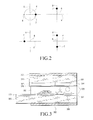
- FIG. 2 illustrates an example of a location of a circular dot in a pattern formed in a display apparatus for a conventional electronic-pen inputting scheme.
- a circular dot (7) in a conventional pattern is disposed to be close to a point (6) where horizontal and vertical raster lines (8) intersect, and a value of the circular dot may be determined based on a distance between the corresponding intersecting point (6) and the circular dot (7) and locational directions of the corresponding intersecting point (6) and the circular dot (7) so that the value may be used for determining the location.
- the digital paper (1) corresponds to a paper-based scheme and thus, the digital paper (1) on which a pattern is separately printed may need to be attached on an LCD panel when the digital paper (1) is used in a display apparatus such as a liquid crystal display (LCD) and the like, and there is a drawback in that an electronic-pen may not be applicable in a region where the digital paper (1) is not attached.
- LCD liquid crystal display
- the LCD panel may be formed of a subpixel corresponding to one of color filters from among an R color filter, a G color filter, and a B color filter, and a black matrix.
- the display panel When the digital paper (1) is attached on a surface of the display panel and is used, the display panel may become thick. Also, when a subpixel is covered by the digital paper (1), luminance of the display may be deteriorated. Also, when a material that reflects an IR light source, as opposed to a paint that absorbs the IR, is used for producing the pattern of the digital paper (1), the subpixel of the display may be affected and thus, a contrast ratio (brightness) and the luminance may be deteriorated.
- a size of a screen of the display apparatus has been increased and a resolution has been more and more increased and thus, an amount of information to be used for recognizing a location indicated by an electronic-pen in the display screen has been also increased. Therefore, in a display apparatus having a huge size and a high resolution, a code pattern for recognizing information associated with a location of an electronic-pen may need to be information-intensive.
- a code pattern for recognizing information associated with a location of an electronic-pen may need to be information-intensive.
- FHD full high definition
- UHD ultra high definition
- the conventional method that uses the digital paper (1) is associated with a physical manufacturing scheme, it may be inefficient to manufacture an information-intensive code pattern.
- a portion of the code pattern of the digital paper (1) may lose or may have an error value, there may be difficulty in checking the loss and the error.
- the conventional method that uses the digital paper (1) may use only a predetermined pattern once the pattern is determined and thus, technology leakages may readily occur.
- an aspect of the present invention is to solve the above-mentioned problems occurring in the prior art, and to provide a display apparatus including a pattern that does not affect a thickness of a display panel and is capable of securing luminance and a contrast ratio of a display screen when an input is determined in the display apparatus, and a method of generating a pattern in the display apparatus.
- Another aspect of the present invention is to provide a display apparatus including a pattern that is capable of intensively representing location information of a pixel so that a location of an input is determined in the display apparatus having a huge size and a high resolution, and a method of generating a pattern in the display apparatus.
- Another aspect of the present invention is to provide a display apparatus including a pattern to be used for checking an error when a portion of the pattern indicating a location of a pixel is lost or has an error, and a method of generating a pattern in the display apparatus.
- Another aspect of the present invention is to provide a display apparatus including an encrypted pattern that is difficult to be intuitively decrypted and prevents the leakage of technology associated with the pattern, and a method of generating a pattern in the display apparatus.
- a display apparatus including a pattern, the apparatus including a plurality of color filters corresponding to subpixels forming pixels of the display apparatus, and a black matrix formed among the plurality of color filters, and the plurality of color filters includes a pattern indicating an absolute location of each pixel of the display apparatus.
- a method of generating a pattern in a display apparatus including determining a basic pattern block size to indicate an absolute location of a pixel on a display panel, determining points where a plurality of holes are to be formed in subpixels included in each block region determined based on the basic pattern block size, and the plurality of holes are used for calculating an absolute location of a corresponding pixel, and generating a pattern by forming a corresponding hole in each point based on an absolute location of a pixel included in each block region, among the points where the plurality of holes are to be formed.
- the present invention proposes a pattern that is applicable to a display apparatus used in an electronic device such as a portable phone, a computer, an electronic blackboard, a tablet PC, an electronic-book, and the like and that is used for indicating a location of a pixel of a display panel, and a pattern generating method.
- a pattern indicating a location of a pixel formed of subpixels may be formed in the corresponding subpixels of a display apparatus including pixels formed of subpixels (R,G, and B). Therefore, embodiments of the present invention may detect the pattern formed in the subpixels of the display apparatus through use of a camera, and may decrypt location and gesture information based on the detected pattern.
- the display apparatus may correspond to any of devices including pixels formed of subpixels, such as a liquid crystal display (LCD), a plasma display panel (PDP), an organic light-emitting display (OLED), an electronic paper, and the like.
- FIG. 3 illustrates a section of a liquid crystal panel of a display apparatus according to an embodiment of the present invention.
- a foreside polarizing plate 302 is disposed on a foreside of the liquid crystal panel
- a color filter substrate 311 is disposed below the foreside polarizing plate 302
- a black matrix 301 and a color filter 304 are disposed below the color filter substrate 311.
- a thin film transistor (TFT) substrate is disposed below the black matrix 301 and the color filter 304.
- TFT thin film transistor
- a common electrode (ITO) 310 and a pixel electrode (ITO) 307 are disposed on a TFT-array substrate 308.
- Two alignment layers 305, a spacer 303, a capacitance storage (CS) 306, a sealant 309 are included between the common electrode 310 and the pixel electrode 307.
- a backside polarizing plate 302 is disposed below the TFT-array substrate 308.
- the black matrix 301 indicating a boundary in the color filter 304 may include a material or a structure that is capable of absorbing a light source, or may include a material or a structure that selectively reflects a light source.
- the black matrix 301 may be formed of carbon black that is an IR absorber.
- the color filter 304 may be formed of an R color filter, a G color filter, and B color filter. Each of the R color filter, the G color filter, and B color filter may correspond to a subpixel, and a set of the R, G, and B color filters may correspond to a single pixel.
- FIG. 4 illustrates subpixel regions and a black matrix region according to an embodiment of the present invention.
- a pattern that is capable of determining a location of a pixel through use of subpixels 32, 34, and 36 and the black matrix 301 may be generated, the location of the pixel may be detected through use of a device (an electronic-pen and the like) that is capable of capturing the pattern and decrypting the captured pattern, and a location of an input of the electronic-pen and an input of a gesture may be recognized based on the detected location.
- a device an electronic-pen and the like
- FIG. 5 illustrates a pattern to be used for determining a location of a pixel based on the subpixel regions and the black matrix region according to an embodiment of the present invention.
- each of subpixels that is, R, G, and B, may include a single hole or a plurality of holes in a predetermined internal location based on a pattern that is predetermined for determining a location of a pixel.
- the hole is in a shape formed by leading a black matrix region into each subpixel region, that is, R, G, and B, and may be formed of the same material as a material of the black matrix region.
- the hole may be formed of another material that may be recognized to be a pattern in R, G, and B regions, and may be disposed in another location.
- FIG. 6 illustrates an example where holes are disposed according to an embodiment of the present invention. As illustrated in FIG. 6 , it is desirable that holes are separately disposed to have a maximum interval and to not overlap each other so as to be clearly recognized.
- Holes included in subpixels may include a dent hole, an X coordinate hole, a Y coordinate hole, and an error detection hole.
- the dent hole is a reference for calculating an absolute location value of a pixel, and may be formed on a point where the dent hole is readily distinguished from other holes.
- the X coordinate hole may be formed on a point indicating a value to be used for calculating a horizontal-coordinate value of a pixel.
- the Y coordinate hole may be formed on a point indicating a value to be used for calculating a vertical-coordinate value of the pixel.
- the error detection hole may be formed on a point indicating a value to be used for determining whether the points where the X coordinate hole and the Y coordinate hole are formed are correct.
- the subpixels may include a subpixel including a dent hole, a subpixel including an X coordinate hole, a subpixel including a Y coordinate hole, and a subpixel including an error detection hole.
- FIG. 5 illustrates a 2 x 2 pixels-based pattern structure.
- a pattern for indicating an absolute location of each of the 2 x 2 pixels is formed in 12 subpixels included in the 2 x 2 (4) pixels.
- FIG. 5 illustrates points where holes are to be formed for indicating a pattern corresponding to an absolute location of a pixel of a display apparatus that supports a resolution of up to 4802 x 2744 in a X coordinate value (width) x a Y coordinate value (height).
- a dent hole 40 is formed on a single subpixel corresponding to adent subpixel to indicate a reference for calculating an absolute location of a pixel.
- 7 septenary numbers (X0, X1, X2, X3, Y1, Y2, and Y3) and one quaternary number Y0 may be used as the X coordinate value and the Y coordinate value.
- FIG. 7 illustrates an example of a point corresponding to a hole that is formed in a subpixel according to an embodiment of the present invention.
- the diagram (a) of FIG. 7 shows points where holes are to be formed when a septenary number is used.
- seven points 61 through 67 may indicate points indicating values of 0 through 6, respectively, and a X coordinate value may be calculated based on Equation 1.
- X coordinate value 73 ⁇ X ⁇ 3 + 72 ⁇ X ⁇ 2 + 7 ⁇ X ⁇ 1 + X ⁇ 0
- position holes may be formed on seven points in four subpixels (Y0, Y1, Y2, and Y3) for 2744 which is a maximum value of a Y value.
- the seven points in the subpixels of Y1, Y2, and Y3 may indicate values of 0 through 6, respectively, and the values of the seven points in the subpixel of Y0 may be different since the subpixel of Y0 uses a quaternary number.
- a point where a hole is formed in the subpixel corresponding to Y0 is illustrated in the diagram (b) of FIG. 7 . Referring to the diagram (b) of FIG. 7 , the seven points in the subpixel corresponding to Y0 may have values in a range of 0 through 3. Therefore, the Y coordinate value may be calculated based on Equation 2.
- Y coordinate value 72 ⁇ 1 ⁇ Y ⁇ 3 + 7 ⁇ 4 ⁇ Y ⁇ 2 + 4 ⁇ Y ⁇ 1 + Y ⁇ 0
- Parity holes may be formed on the seven points in three subpixels p, q, and r by applying a parity check scheme so as to determine whether the points where the X coordinate hole and the Y coordinate hole are formed are correct, that is, so as to determine whether an error occurs.
- the parity check scheme may refer to a scheme that additionally adds a parity checker bit so that a number of bits indicating 1 in a conventional binary code to be an even number of bits or an odd number of bits, and detects an error.
- a septenary number is used and thus, a parity checker may have a value in a range of 0 through 6.
- Points corresponding to the seven holes in p, q, and r subpixels may be points for indicating a parity bit, that is, a value obtained by adding up values of predetermined position holes. Therefore, the values of p, q, and r may be calculated based on parity check equations of Equation 3.
- p modulo / X ⁇ 3 + Y ⁇ 1 + X ⁇ 0
- q modulo ⁇ 7 ⁇ X ⁇ 2 + Y ⁇ 2
- r modulo ⁇ 7 ⁇ X ⁇ 1 + Y ⁇ 3 + Y ⁇ 0
- the p value may be a reference for determining whether an error occurs with respect to values of X3, Y1, and X0.
- the q value may be a reference for determining whether an error occurs with respect to values of X2 and Y2.
- the r value may be a reference for determining whether an error occurs with respect to values of X1, Y3, and Y0.
- the problem may be solved based on a scheme that includes position holes associated with the same coordinate axis in different parity check equations. Since an X axis and a Y axis have 4 position holes and thus, a total of 4 parity check equations may be required. However, excluding the dent hole and the position holes, available holes may need to be included in three subpixels and thus, up to 3 parity check equations may be used. Accordingly, position holes associated with the same coordinate axis may be inevitably included in a single parity check equation.
- an error occurring in a position hole corresponding to the lowest digit may have the lowest probability of affecting a position hole corresponding to the highest digit and thus, it is desirable to use a scheme that includes the position hole corresponding to the lowest digit and the position hole corresponding to the highest digit in the same parity check equation, as shown in the p, q, and r equations of Equation 3.
- a pattern may be formed based on a single pixel and a pattern may be formed based on various pixel units such as a 2x3 pixel unit, a 3x3 pixel unit, and the like, and a point and a value of a hole may be appropriately used based on a corresponding pixel unit.
- the pattern formed in the display apparatus configured as described in the foregoing may have a regular rule and thus, the pattern may be readily decrypted when the rule is recognized. Therefore, an embodiment of the present invention may provide an encrypted pattern so that the pattern formed in the display apparatus may not be readily decrypted.
- the pattern may be generated based on a shuffle table so that the generated pattern may not be readily imitated.
- FIG. 8 illustrates an example of a shuffle table according to an embodiment of the present invention.
- the diagram (a) of FIG. 8 is an example of a shuffle table for encrypting
- the diagram (b) of FIG. 8 is an example of a shuffle table for inverse-encrypting.
- holes included in each subpixel excluding a dent may be formed in locations having values in a range of 0 through 6 and thus, a shuffle value (s(x)) for converting a value (x) in a range of 0 through 6 may be arranged in a table, and a location of each hole may be converted into a location corresponding to a shuffle value so that an encrypted pattern may be provided. For example, when a point where an original hole is formed corresponds to a point indicating 0, a hole may be formed on a point indicating 4 based on the shuffle table.
- a plurality of shuffle tables may be used, a predetermined shuffle table from among the plurality of shuffle tables may be determined, and the encrypted pattern may be provided.
- a predetermined first shuffle table may be used for parity holes of p, q, and r that have a high frequency of change in points where holes are formed and for a position hole of Y0.
- a second shuffle table to be applied to the remaining holes may be determined based on the first shuffle table value associated with the parity holes of p, q, and r, and the position hole of Y0, and points where the remaining holes are formed may be converted into points corresponding to values based on the determined second shuffle table.
- FIG. 9 illustrates an example of a shuffle table determining scheme for encrypting position holes according to an embodiment of the present invention.
- a c value may be a shuffle value that is obtained by converting parity holes of p, q, and r, and a position hole of Y0 through use of a first shuffle table, and may indicate a value that is a reference for determining a second shuffle table to be applied to remaining holes.
- Sc(x) may indicate the second shuffle table determined based on the reference value. Values for the remaining holes may be determined based on the second shuffle table and an encrypted pattern may be provided.
- the second shuffle table may be determined based on values of other holes, in addition to a scheme that determines the second shuffle table based on the parity holes of p, q, and r, and the position hole of Y0.
- FIG. 10 illustrates a process of generating a pattern in a display apparatus according to an embodiment of the present invention.
- the display apparatus may determine a basic pattern block size required for obtaining an absolute location of a single pixel on a display panel in operation 101.
- a pattern indicating the absolute location of the pixel may be formed on a plurality of pixels (for example, 2x2 pixels).
- a size of the plurality of pixels where the pattern is formed to obtain the absolute location of the pixel may be referred to as the basic pattern block size.
- the display apparatus may determine points where a dent hole corresponding to a reference and position holes for indicating the absolute location of the pixel are to be formed in subpixels for each block region in operation 104. In this example, points where parity holes for checking an error of the position holes for indicating the absolute location of the pixel are to be formed may also be determined.
- a point for a dent hole corresponding to a single subpixel for indicating a reference to be used for calculating an absolute location value of the pixel may be determined.
- points for 7 position holes may be determined in 8 subpixels through use of 7 septenary numbers (X0, X1, X2, X3, Y1, Y2, and Y3) and one quaternary number (YO) as an X coordinate value and a Y coordinate value.
- Points for 7 parity holes may be determined in remaining 3 subpixels so as to check an error of the position holes.
- the display apparatus may calculate values of the position holes corresponding to the location of the pixel to be indicated by each block region, and may encrypt the calculated values in operation 106.
- values of position holes to be formed in 8 subpixels (X0, X1, X2, X3, Y1, Y2, Y3, and Y0) may be obtained through use of Equation 1 and Equation 2, so as to indicate the location of the pixel (an X coordinate value and a Y coordinate value).
- the values of the position holes may be converted into encrypted values based on a shuffle table that is described in the foregoing.
- the display apparatus may form the dent hole and the position holes on the point where the dent hole is to be formed and points corresponding to the encrypted values of the position holes, and may generate a pattern indicating the location of the pixel in operation 108.
- parity holes may also be formed and may be included in the pattern so as to check errors.
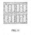
- FIG. 11 illustrates an example of a pattern formed to indicate a location of a pixel in a display apparatus according to an embodiment of the present invention.
- the pattern generated according to embodiments of the present invention may be recognized by an inputting device including a camera, such as an electronic-pen and the like, and a location of a corresponding pixel may be detected and thus, inputting may be performed based on the detected location value of the pixel.
- an inputting device including a camera, such as an electronic-pen and the like, and a location of a corresponding pixel may be detected and thus, inputting may be performed based on the detected location value of the pixel.
- inputting may be performed by forming a pattern indicating a location of a pixel in subpixels of a display apparatus and thus, a display panel may not affect a thickness as opposed to a digital paper, and luminance and a contrast ratio of a display screen may be secured.
- a pattern for indicating a location of a pixel may be formed in subpixels of a display apparatus based on a number of predetermined holes and locations of the holes, and location information of the pixel may be intensively represented and thus, the embodiments of the present invention may be applicable to a display apparatus having a huge size and a high resolution.
- a pattern may be formed based on an encrypted value and thus, the pattern of a display apparatus may not be intuitively decrypted and the leakage of technology associated with the pattern may be prevented.
Landscapes
- Engineering & Computer Science (AREA)
- General Engineering & Computer Science (AREA)
- Theoretical Computer Science (AREA)
- Physics & Mathematics (AREA)
- General Physics & Mathematics (AREA)
- Human Computer Interaction (AREA)
- Nonlinear Science (AREA)
- Control Of Indicators Other Than Cathode Ray Tubes (AREA)
- Chemical & Material Sciences (AREA)
- Crystallography & Structural Chemistry (AREA)
- Mathematical Physics (AREA)
- Optics & Photonics (AREA)
- Optical Filters (AREA)
- Devices For Indicating Variable Information By Combining Individual Elements (AREA)
Applications Claiming Priority (1)
| Application Number | Priority Date | Filing Date | Title |
|---|---|---|---|
| KR1020110099423A KR20130035144A (ko) | 2011-09-29 | 2011-09-29 | 패턴을 구비한 디스플레이 장치 및 디스플레이 장치에서 패턴 생성 방법 |
Publications (2)
| Publication Number | Publication Date |
|---|---|
| EP2575010A2 true EP2575010A2 (de) | 2013-04-03 |
| EP2575010A3 EP2575010A3 (de) | 2016-11-02 |
Family
ID=47325798
Family Applications (1)
| Application Number | Title | Priority Date | Filing Date |
|---|---|---|---|
| EP12186591.9A Withdrawn EP2575010A3 (de) | 2011-09-29 | 2012-09-28 | Anzeigevorrichtung mit Muster und Verfahren zum Erzeugen von Muster in Anzeigevorrichtung |
Country Status (3)
| Country | Link |
|---|---|
| US (1) | US20130082907A1 (de) |
| EP (1) | EP2575010A3 (de) |
| KR (1) | KR20130035144A (de) |
Families Citing this family (3)
| Publication number | Priority date | Publication date | Assignee | Title |
|---|---|---|---|---|
| KR101974483B1 (ko) | 2012-12-03 | 2019-05-02 | 삼성전자주식회사 | 패턴을 구비한 디스플레이 장치 및 패턴을 구비한 디스플레이 장치에서 화소 위치 검출 방법 |
| EP3049481A4 (de) * | 2013-09-27 | 2017-05-31 | Saint-Gobain Performance Plastics Corporation | Silikonartikel, röhre und verfahren zur herstellung eines artikels |
| KR20230013686A (ko) * | 2021-07-16 | 2023-01-27 | 삼성디스플레이 주식회사 | 표시 장치 및 이를 포함하는 센싱 시스템 |
Family Cites Families (9)
| Publication number | Priority date | Publication date | Assignee | Title |
|---|---|---|---|---|
| JP4384293B2 (ja) * | 1999-07-06 | 2009-12-16 | エーユー オプトロニクス コーポレイション | 液晶表示パネル、表示装置、識別マーク検出装置、検出表示システム、tftアレイ・リペア装置及び識別マーク検出方法 |
| SE517445C2 (sv) * | 1999-10-01 | 2002-06-04 | Anoto Ab | Positionsbestämning på en yta försedd med ett positionskodningsmönster |
| KR100603842B1 (ko) * | 2000-02-18 | 2006-07-24 | 엘지.필립스 엘시디 주식회사 | 확인용 인식마크를 포함하는 컬러필터 |
| JP4235468B2 (ja) * | 2003-02-28 | 2009-03-11 | キヤノン株式会社 | 半導体製造装置 |
| TW200613813A (en) * | 2004-05-05 | 2006-05-01 | Koninkl Philips Electronics Nv | Display device |
| GB2419714A (en) * | 2004-10-28 | 2006-05-03 | Hewlett Packard Development Co | Allocation of data-encoding pattern |
| US20060242562A1 (en) * | 2005-04-22 | 2006-10-26 | Microsoft Corporation | Embedded method for embedded interaction code array |
| US7790340B2 (en) * | 2007-04-20 | 2010-09-07 | Photronics, Inc. | Photomask with detector for optimizing an integrated circuit production process and method of manufacturing an integrated circuit using the same |
| JP4154700B1 (ja) * | 2007-06-21 | 2008-09-24 | 健治 吉田 | カード面の読取・命令実行方法 |
-
2011
- 2011-09-29 KR KR1020110099423A patent/KR20130035144A/ko not_active Ceased
-
2012
- 2012-09-27 US US13/628,645 patent/US20130082907A1/en not_active Abandoned
- 2012-09-28 EP EP12186591.9A patent/EP2575010A3/de not_active Withdrawn
Non-Patent Citations (1)
| Title |
|---|
| None |
Also Published As
| Publication number | Publication date |
|---|---|
| EP2575010A3 (de) | 2016-11-02 |
| US20130082907A1 (en) | 2013-04-04 |
| KR20130035144A (ko) | 2013-04-08 |
Similar Documents
| Publication | Publication Date | Title |
|---|---|---|
| TWI623776B (zh) | 設計光學基板的方法 | |
| CN104981754B (zh) | 用于降低输入装置中干扰的影响的系统和方法 | |
| US20120242606A1 (en) | Trace design for reduced visibility in touch screen devices | |
| US10126865B2 (en) | Touch control display panel and display device | |
| WO2007022397A1 (en) | Embedded interaction code enabled display | |
| CN104777952A (zh) | 减轻集成输入装置中电极干扰 | |
| CN103677256B (zh) | 呈现触觉图像的方法和用于执行该方法的触摸屏设备 | |
| JP2017220015A (ja) | 入力検出装置及びタッチ検出機能付き表示装置 | |
| CN105069330A (zh) | 密码模糊输入方法及装置 | |
| US9507440B2 (en) | Apparatus and method to detect coordinates in a pen-based display device | |
| JP5778592B2 (ja) | 表示装置、タッチ検出装置および電子機器 | |
| US11334199B2 (en) | Spatially encoded sensor electrodes | |
| WO2013065272A1 (ja) | タッチパネル及びタッチパネル付き表示装置 | |
| US20130082907A1 (en) | Display apparatus including a pattern and method for generating a | |
| US9146625B2 (en) | Apparatus and method to detect coordinates in a penbased display device | |
| CN106445247A (zh) | 触控面板及显示装置 | |
| CN104461164A (zh) | 触控显示面板和触控显示装置 | |
| JP6006380B2 (ja) | 表示装置、タッチ検出装置および電子機器 | |
| KR101974483B1 (ko) | 패턴을 구비한 디스플레이 장치 및 패턴을 구비한 디스플레이 장치에서 화소 위치 검출 방법 | |
| US20170192552A1 (en) | Elliptical capacitive sensor electrode pattern and sensing therewith | |
| EP2960753B1 (de) | Optische berührungsanzeigevorrichtung und verfahren zu ihrer ansteuerung | |
| US8564570B2 (en) | Optical touch apparatus and operating method thereof | |
| KR102338710B1 (ko) | 광학 터치 디스플레이 장치 및 이의 구동방법 | |
| JP2015153277A (ja) | 表示装置 | |
| CN103218088B (zh) | 光学触摸显示装置及光学触摸屏 |
Legal Events
| Date | Code | Title | Description |
|---|---|---|---|
| PUAI | Public reference made under article 153(3) epc to a published international application that has entered the european phase |
Free format text: ORIGINAL CODE: 0009012 |
|
| AK | Designated contracting states |
Kind code of ref document: A2 Designated state(s): AL AT BE BG CH CY CZ DE DK EE ES FI FR GB GR HR HU IE IS IT LI LT LU LV MC MK MT NL NO PL PT RO RS SE SI SK SM TR |
|
| AX | Request for extension of the european patent |
Extension state: BA ME |
|
| PUAL | Search report despatched |
Free format text: ORIGINAL CODE: 0009013 |
|
| AK | Designated contracting states |
Kind code of ref document: A3 Designated state(s): AL AT BE BG CH CY CZ DE DK EE ES FI FR GB GR HR HU IE IS IT LI LT LU LV MC MK MT NL NO PL PT RO RS SE SI SK SM TR |
|
| AX | Request for extension of the european patent |
Extension state: BA ME |
|
| RIC1 | Information provided on ipc code assigned before grant |
Ipc: G02F 1/133 20060101ALI20160928BHEP Ipc: G06F 3/03 20060101AFI20160928BHEP Ipc: G06F 3/041 20060101ALI20160928BHEP |
|
| STAA | Information on the status of an ep patent application or granted ep patent |
Free format text: STATUS: THE APPLICATION IS DEEMED TO BE WITHDRAWN |
|
| 18D | Application deemed to be withdrawn |
Effective date: 20170503 |