EP2573829A2 - Light emitting diode module - Google Patents
Light emitting diode module Download PDFInfo
- Publication number
- EP2573829A2 EP2573829A2 EP12198155A EP12198155A EP2573829A2 EP 2573829 A2 EP2573829 A2 EP 2573829A2 EP 12198155 A EP12198155 A EP 12198155A EP 12198155 A EP12198155 A EP 12198155A EP 2573829 A2 EP2573829 A2 EP 2573829A2
- Authority
- EP
- European Patent Office
- Prior art keywords
- module according
- led module
- outer dam
- central filling
- dam
- Prior art date
- Legal status (The legal status is an assumption and is not a legal conclusion. Google has not performed a legal analysis and makes no representation as to the accuracy of the status listed.)
- Granted
Links
Images


Classifications
-
- H—ELECTRICITY
- H10—SEMICONDUCTOR DEVICES; ELECTRIC SOLID-STATE DEVICES NOT OTHERWISE PROVIDED FOR
- H10H—INORGANIC LIGHT-EMITTING SEMICONDUCTOR DEVICES HAVING POTENTIAL BARRIERS
- H10H20/00—Individual inorganic light-emitting semiconductor devices having potential barriers, e.g. light-emitting diodes [LED]
- H10H20/80—Constructional details
- H10H20/85—Packages
- H10H20/852—Encapsulations
-
- H—ELECTRICITY
- H10—SEMICONDUCTOR DEVICES; ELECTRIC SOLID-STATE DEVICES NOT OTHERWISE PROVIDED FOR
- H10F—INORGANIC SEMICONDUCTOR DEVICES SENSITIVE TO INFRARED RADIATION, LIGHT, ELECTROMAGNETIC RADIATION OF SHORTER WAVELENGTH OR CORPUSCULAR RADIATION
- H10F77/00—Constructional details of devices covered by this subclass
- H10F77/30—Coatings
- H10F77/306—Coatings for devices having potential barriers
-
- H—ELECTRICITY
- H10—SEMICONDUCTOR DEVICES; ELECTRIC SOLID-STATE DEVICES NOT OTHERWISE PROVIDED FOR
- H10F—INORGANIC SEMICONDUCTOR DEVICES SENSITIVE TO INFRARED RADIATION, LIGHT, ELECTROMAGNETIC RADIATION OF SHORTER WAVELENGTH OR CORPUSCULAR RADIATION
- H10F77/00—Constructional details of devices covered by this subclass
- H10F77/50—Encapsulations or containers
-
- H—ELECTRICITY
- H10—SEMICONDUCTOR DEVICES; ELECTRIC SOLID-STATE DEVICES NOT OTHERWISE PROVIDED FOR
- H10H—INORGANIC LIGHT-EMITTING SEMICONDUCTOR DEVICES HAVING POTENTIAL BARRIERS
- H10H20/00—Individual inorganic light-emitting semiconductor devices having potential barriers, e.g. light-emitting diodes [LED]
- H10H20/80—Constructional details
- H10H20/85—Packages
- H10H20/855—Optical field-shaping means, e.g. lenses
- H10H20/856—Reflecting means
-
- H—ELECTRICITY
- H10—SEMICONDUCTOR DEVICES; ELECTRIC SOLID-STATE DEVICES NOT OTHERWISE PROVIDED FOR
- H10H—INORGANIC LIGHT-EMITTING SEMICONDUCTOR DEVICES HAVING POTENTIAL BARRIERS
- H10H20/00—Individual inorganic light-emitting semiconductor devices having potential barriers, e.g. light-emitting diodes [LED]
- H10H20/80—Constructional details
- H10H20/85—Packages
- H10H20/852—Encapsulations
- H10H20/854—Encapsulations characterised by their material, e.g. epoxy or silicone resins
-
- H—ELECTRICITY
- H10—SEMICONDUCTOR DEVICES; ELECTRIC SOLID-STATE DEVICES NOT OTHERWISE PROVIDED FOR
- H10W—GENERIC PACKAGES, INTERCONNECTIONS, CONNECTORS OR OTHER CONSTRUCTIONAL DETAILS OF DEVICES COVERED BY CLASS H10
- H10W74/00—Encapsulations, e.g. protective coatings
-
- H—ELECTRICITY
- H10—SEMICONDUCTOR DEVICES; ELECTRIC SOLID-STATE DEVICES NOT OTHERWISE PROVIDED FOR
- H10W—GENERIC PACKAGES, INTERCONNECTIONS, CONNECTORS OR OTHER CONSTRUCTIONAL DETAILS OF DEVICES COVERED BY CLASS H10
- H10W90/00—Package configurations
- H10W90/701—Package configurations characterised by the relative positions of pads or connectors relative to package parts
- H10W90/751—Package configurations characterised by the relative positions of pads or connectors relative to package parts of bond wires
- H10W90/756—Package configurations characterised by the relative positions of pads or connectors relative to package parts of bond wires between a chip and a stacked lead frame, conducting package substrate or heat sink
Definitions
- the second disadvantage of the globe-top cover is the low mechanical stability of the LED modules which is a disadvantage for the handling and mounting of the LED modules.
- silicones are used as resins for the globe-top.
- these rubber-like materials apply a high mechanical stress to bond wires if the spherical shape of the globe-top is warped.
- the outer ring is raised higher from the board than the LED-chip.
- the cross-sectional shape of the dam 2 can be controlled by the diameter of the dispensing needle used, the flow characteristics of the liquid dam material and the flow (dispensing) speed.
- the entire material of the ring will have a non-transparent and preferably white reflecting appearance.
- the reflection from light from the LED die 1 occurs at the inner face 11 of the ring (or "dam") 2 reflecting light back to the interior of the ring 1 and away from the LED die 1.
- the cover according to the present invention can protect the opening 6 of the casing of the light erasable memory device 7, which opening is designed for the light erasing process.
- the arrangement as shown in Fig. 5 provides for an improved light feeding from the light source to the optical fibre.
Landscapes
- Led Device Packages (AREA)
- Structures Or Materials For Encapsulating Or Coating Semiconductor Devices Or Solid State Devices (AREA)
- Encapsulation Of And Coatings For Semiconductor Or Solid State Devices (AREA)
Abstract
- mounting a electronic and/or optoelectronic chip on a board,
- making on the board an outer ring made from a liquid resin, the outer ring surrounding the electronic and/or optoelectronic chip,
- making a central filling of the volume defined by the outer ring, the central filling being made from a liquid resin and covering the top surface of the electronic and/or optoelectronic chip,
- curing in one single step the resin of the outer ring and the central filling and making a chemically linked interface between the outer ring and the central filling.
Description
- The present invention relates to the field of optoelectronic components, such as for example LED modules and light sensors. The cover is designed to allow the directed passage of light to and/or from the component.
- The invention also relates to a method for manufacturing such covers and LED modules being provided with such covers.
- From the state of the art it is known to cover so called COB (chip-on-board) LED modules with a so called globe-top which is based on a heat-curable resin. Such a globe-top is usually applied with standard dispensing equipment. However, the performance of LED modules having such a globe-top is not satisfying all requirements of different application fields. One of the main disadvantages actually is the directive characteristics, i.e. the wide emission angle, which is not well suited for using such a LED module with secondary optics, such as for example lenses or light guides.
- In order to have a smaller emission angle of the light emitted by COB LED modules the die is sometimes placed in a cavity with a reflecting wall. However, due to the spherical shape of the top surface of the globe-top, the contribution of the reflecting wall on the emission angle is not satisfying.
- The second disadvantage of the globe-top cover is the low mechanical stability of the LED modules which is a disadvantage for the handling and mounting of the LED modules. In this context is to be noted that based on the requirements on a high UV stability, usually silicones are used as resins for the globe-top. Unfortunately, these rubber-like materials apply a high mechanical stress to bond wires if the spherical shape of the globe-top is warped.
-
WO 2006/017484A1 proposes a dam-and-fill technology in order to protect parts of a printed circuit board against electric short circuits. - Therefore, it is the object of the present invention to propose an improved cover for optoelectronic components, which cover allows the directed passage of light to and/or from the component.
- This object is achieved by means of the features of the independent claims. The dependent claims develop further the central idea of the present invention.
- According to a first aspect of the invention a cover for optoelectronic components, such as for example LED diodes, is proposed. The cover allows for a passage and preferably a directed passage of light to and/or from the component. The cover comprises an outer non-transparent and preferably reflective dam and a central filling, which central filling has been filled into the outer ring preferably after the manufacturing of the outer ring. The outer ring and the central filling are respectively made from a cured resin. The central filling is chemically linked to the outer ring across the interface.
- Note that "outer dam" does not represent any limitation as to the shape, as long as the dam can act as a dam surrounding the central filling and being stable in shape even in the uncured state.
- The resin can be e.g. silicone.
- The dam can comprise reflecting particles such as for example white pigments. The reflecting particles are preferably present throughout the bulk of the outer ring material. The dam thus has the role of a reflector applied in the liquid state on a board.
- The outer ring can comprise 10 to 60 weight % of the reflecting particles.
- The resin of the outer ring and the central filling can have the same chemical structure, e.g. they can be chemically identical.
- The resin of the outer ring can be selected to have a storage modulus of more than 1000 Pa before being cured.
- The resin of the outer ring can be selected such that it has for example a viscosity of more than 100 Pa*s when measured at a shear rate of 1 1/s, again before being cured.
- The material of the outer ring can comprise particulate material such as e.g. silica, which particular material or fine grained material can be used in order to set the desired rheological properties of the uncured dam resin.
- The height of the outer ring can be equal to or more than 1mm.
- The mean thickness of the outer ring can be selected according to the requirements of the final element. For a diameter of approx. 5 mm the thickness can be equal to or less than 0.5mm. For larger diameters the thickness is adjusted to more than 0.5 mm, for smaller diameters the thickness might be less than 0.5 mm.
- The inner diameter of the dam can be as small as e.g. 0.1 to 1mm.
- The invention also relates to a light-erasable memory devices, light-sensitive sensors and LED modules having such covers.
- The invention can particularly be used for a LED module comprising a LED chip mounted on a board as well as a cover. The cover comprises an outer ring and a central filling, which has been filled into the outer ring and at least partially on top of the LED chip after the outer ring has been made on the board surrounding the LED chip.
- The central filling can be made from a transparent resin, such as e.g. silicone.
- The central filling can comprise color conversion particles which convert light emitted from the LED chip into light of a second, lower frequency spectrum.
- The inner wall of the outer ring can be distanced from the LED chip, such that the distance between the outer ring and the LED chip is filled with the central filling which thus is also in contact with the board on which the LED chip is mounted e.g. in a chip-on-board technology.
- The central filling can fill the entire volume defined by the outer ring such that the top surface of the filling is on the same level as the maximum height of the outer ring.
- Preferably the outer ring is raised higher from the board than the LED-chip.
- The invention also relates to a method for manufacturing a cover for electronic or optoelectronic components. An outer ring made from a liquid resin is first dispensed. This outer ring is then filled with a liquid resin. Finally, in one single step, the resin of the outer ring and the resin of the central filling are cured and a chemically linked interface between the outer ring and the central filling is provided which guarantees a stronger adhesion between the central filling and the outer ring.
- Further aspects, advantages and objects of the present invention will become evident from the following detailed explanation of embodiments of the present invention when taking in conjunction with the figures of the enclosed drawings.
-
Fig. 1 shows schematically a side view of a LED module having a cover according to the present invention. -
Fig. 2 shows a top view of a LED module with a cover according to the present invention. -
Fig. 3 shows a perspective view of a cover of the present invention. -
Fig. 4 shows the use of a cover according to the present invention together with a light-erasable storage device, and -
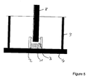
Fig. 5 shows the use of the present invention in connection with a light source and a light guiding element. - To start with, a method for manufacturing a cover for optoelectronic components according to the present invention will be explained.
- As the cover has a role a optical element, its precision has to go far beyond the precision necessary for purely protective purposes as known from
WO 2006/017484A1 . - The following method will be explained in the context of producing a cover for a LED module as shown in
Fig. 1 . - In a first step, a ring-shaped dam (torus) of a liquid resin is dispensed around the LED chip (LED diode) 1, which is placed on a
board 4. - Preferably a plane board without recessions is used, as the reflective effect of walls of a recession can be achieved by the dam walls.
- Dispensing techniques for resins and silicones are known as such from the prior art. Due to the dispensing technique the cross-sectional view of the dam tapers to the
peak 10 of thedam 2. Thus the inner face 11 ofdam 2 is inclined and preferably is steeper at its upper part which can be of advantage for reflection purposes. - The cross-sectional shape of the
dam 2 can be controlled by the diameter of the dispensing needle used, the flow characteristics of the liquid dam material and the flow (dispensing) speed. - In the example shown in
Fig. 1 theLED chip 1 is mounted according to the chip-on-board (COB) technology. The bond wires are designated with the reference numeral 5. - The wall of liquid resin is dispensed on the
board 4 around the LED die 1 thus forming a ring. - Preferably the dam material is non-transparent for the wavelength of the light passing through the filling inside the dam.
- Please note that 'ring' in the context of the present description and claims does not constitute any limitation as to the contour of the walls, i.e. the ring does not necessarily have a spherical shape, but can e.g. have the shape of a square, an oval, a rectangular shape etc..
- The circular shape is preferred if only a single optically active element is placed inside the dam (see later on), while a rectangular or oval shape is preferred in case a plurality of optically active elements such as LEDs are placed inside the dam in a row configuration.
- Different base resins can be used for the
ring 2. Preferred materials are silicones due to their high UV stability. - The rheological characteristics of the liquid resin material for building the wall of the
ring 2 have to be well selected such that after the dispensing the uncured resin is stable in shape until it is cured. - To this regard the storage modulus should be rather high and e.g. be at least 1000 Pa. The loss factor should be approximately 0.5.
- The viscosity of the liquid resin should preferably be higher than 200 Pa*s (when measured at a shear rate of 1 1/s). A liquid resin material of such characteristics is suited for achieving a wall e.g. with a height of more than 1mm and a mean thickness of less than 0.5mm.
- In order to adjust the rheological characteristics of the liquid resin material, silica or other particulate material (fine grained material) can be added to the liquid resin.
- As can be seen from
Fig. 1 , preferably thewall 2 is distanced from the LED die 1. - Furthermore, the height of the
ring 2 is set to be higher than the height of the LED die 1. E.g. the height of thering 2 can be twice or three times the height of the LED die 1. - In case a higher light reflectivity of the wall of the
ring 2 is desired, optionally reflecting substances such as e.g. white pigments can be added into the liquid resin material. Examples for such pigments are pigments made from TiO2, BaTiO3, BaSO4 and/or ZrO2. - Preferably, these pigments are added to the liquid resin in an amount of 10% to 60% per weight.
- Thus the entire material of the ring will have a non-transparent and preferably white reflecting appearance. The reflection from light from the LED die 1 occurs at the inner face 11 of the ring (or "dam") 2 reflecting light back to the interior of the
ring 1 and away from the LED die 1. - In a second step of the manufacturing process the volume confined by the inner walls of the self-
stable ring 2 is filled with a liquid filling material. As can be seen fromFig. 1 , this filling is preferably made such that the top level of the filling flushes with the top level of the walls of thering 2. Due to the filling with the liquid resin the top surface 12 of thecentral filling 3 will be preferably flat. - To summarize, liquid uncured resin is filled in a cavity defined by a self-stable dam of uncured resin, which preferably chemically identical, but can be different regarding optical and mechanical characteristics (as the material of the
outer ring 2 can be provided with different "additives" as the material of the central filling 3). - The chemical identity has to be such that the material used for the dam and the filling, respectively, can be cured using the same curing mechanism in order to produce a chemical linking across the interface between the two materials.
- The filling material entirely covers the top surface of the LED die 1. It also covers the space between the LED die 1 and the walls of the ring 2 (if any) and contacts the
board 4 in this gap between the LED die 1 and thering 2. - The material for the
central filling 3 is also a resin and can be e.g. be made from a silicone material. - Preferably, the resin for the
central filling 3 is made from the same material as the resin for thering 2 such that these resins are chemically identical. - For coloured LED modules (e.g. blue, green, amber and red) it is not necessary to add additional fillers to the resin for the
central filling 3. - On the other hand, for white color-conversion LED modules, colour conversion particles can be added to the fill material of the
central filling 3. The type and the amount of the colour conversion particles depends on the desired colour temperature of the LED module, which is known as such from the prior art. Preferably there is an increasing concentration gradient of the color conversion particles from the top to the bottom of the filling, which can be achieved e.g. by allowing the color conversion particles to sink towards the bottom of the filling. - In a third step the liquid resins i.e. the resins of the
central filling 3 and thering 2 are cured. By a single curing cycle both of the materials can be cured and chemically linked together at their interface. - The above-outlined manufacturing process relies on a relatively high mechanical stability of the material of the wall in the uncured "liquid" state. Again, in order to achieve this mechanical stability in the liquid state, additional filling materials such as for example silica can be added to the resin for the
ring 2. - Both for the manufacturing of the
ring 2 as well as for the filling a standard computer controlled dispensing equipment can be used. -
Figures 2 and3 show a top view (Fig. 2 ) and a perspective view (Fig. 3 ) of a LED module having a cover according to the present invention and being mounted in chip-on-board technology. In these examples the material of thering 2 is highly reflective as white pigments have been added throughout the base resin for thering 2. - On the other hand, the resin for the filling 3 is essentially transparent and the bond wires 5 can be seen which are surrounded and stabilized by the material of the
central filling 3. - As will be explained in the following, the present invention is not limited to LED modules regarding this application, but can also be used in connection with other electronic or optoelectronic components.
- In
Fig. 4 a light-erasable memory device such as for example an EEPROM 7 is shown. - The cover according to the present invention can protect the
opening 6 of the casing of the light erasable memory device 7, which opening is designed for the light erasing process. - Due to the "dam-and-fill" coverage according to the present invention, which can be made of highly transparent materials depending on the requirements of the erasing/programming light beam, a protection against environmental influences as well as perfect fit to the erasing/programming light source can be achieved. Especially, the protection against scattered light and stray light is a big advantage of the dam and fill cover according to the present invention. The outer ring thus can not only serve as a reflective element, but additionally or alternatively as an opaque shielding.
- The invention can also be used for light-sensitive sensors such as for example RGB-sensors, infrared sensors or CCD-sensors.
- Also infrared emitters as well as light sensitive light detection devices coated and protected through a cover as explained above are additional field of the application, in particular when the sensor is present as a bare chip in COB or Leadframe technology.
- Finally,
Fig. 5 shows the use of a cover according to the present invention in connection with light guides and optical fibers. - The dam material (ring) 2 provides a mechanical stability, such that it is possible to provide the filling 3 on top of the light source as a very fluid and highly transparent synthetic resin.
- In the example shown in
Fig. 5 there is no gap between thering 2 and thelight source 1 such that the filling material is only present on top of thelight source 1. - Furthermore, the filling 3 is not completely flush with the top of the wall of the
ring 2. - The reference sign 8 designates an optical fiber to which light from the
light source 1 is to be transmitted (transversing the fill material 3). - The
reference sign 9 designates mechanical fixture for optical fibers. - The arrangement as shown in
Fig. 5 provides for an improved light feeding from the light source to the optical fibre.
Claims (26)
- An LED module comprising a LED chip (1) and a cover mounted on a board (4), the cover comprising an outer non-transparent, preferably reflective dam (2),
a central filling (3), which is filled into the outer dam (2), preferably after the manufacturing of the outer dam (2),
wherein the outer dam (2) comprises reflecting particles throughout the bulk of the outer dam material,
wherein the central filling (3) is made from a cured resin, and wherein the resin of the central filling (3) is silicone based. - The LED module according to Claim1.
wherein the outer dam (2) is made from a cured resin. - The LED module according to Claim 2,
wherein the resin of the outer dam (2) is silicone based. - The LED module according to Claim1 to 3,
wherein the inner wall of the outer dam (2) is distanced from the LED chip, such that the distance between the outer dam (2) and LED chip (1) is filled with the central filling (3) and in contact with the board (4) on which the LED chip (1) is mounted. - The LED module according to any of the preceding claims,
wherein the central filling (3) is filled at least partially on top of the LED chip (1). - The LED module according to any of the preceding claims,
wherein the central filling (3) is linked to the outer dam (2) forming a single entity. - The LED module according to any of the preceding claims,
wherein the resin of the outer dam (2) and the central filling (3) have the same chemical structure. - The LED module according to any of the preceding claims,
wherein the resin of the outer dam (2) and the central filling (3) are chemically identical. - The LED module according to any of the preceding claims,
wherein at least the central filling (3) is made from a transparent resin. - The LED module according to any of the preceding claims,
wherein the central filling (3) comprises color conversion particles. - The LED module according to any of the preceding claims,
wherein the outer dam (2) comprises reflecting particles. - The LED module according to claim 11,
wherein the reflecting particles are white pigments from the group of TiO2, BaTiO3, BaSO4 and ZrO2. - The LED module according to any of the preceding claims,
wherein the outer dam (2) comprises 10 to 60 weight % of reflecting particles. - The LED module according to any of the preceding claims, wherein the mean thickness of the outer dam (2) is adjusted for larger diameters than 5mm to more than 0.5mm.
- The LED module according to any of the preceding claims,
wherein the LED chip (1) is mounted on the board (4) according to a chip-on-board technology. - The LED module according to any of the preceding claims,
wherein the central filling (3) fills the entire volume defined by the outer dam (2). - The LED module according to any of the preceding claims,
wherein the outer dam (2) is higher than the LED chip (1). - The LED module according to any of the preceding claims,
wherein the height of the outer dam (2) has at least the height of LED chip (1) to be covered. - The LED module according to any of the preceding claims,
wherein at least the inner wall of the outer dam (2) is light-reflective. - The LED module according to any of the preceding claims,
wherein the outer dam (2) has circular, oval, or rectangular shape. - The LED module according to any of the preceding claims,
wherein the LED chips (1) are in a row configuration placed inside the outer dam (2). - The LED module according to any of the preceding claims,
wherein the outer dam (2) and/or the central filling (3) are made by dispensing. - The LED module according to any of the preceding claims,
wherein the bonding wires (5) are stabilized by the material of the central filling (3). - The LED module according to any of the preceding claims,
wherein the board (4) is preferably a plane board. - The LED module according to any of the preceding claims,
wherein the inner face (11) of the dam (2) is inclined. - The LED module according to any of the preceding claims, wherein the outer dam (2) comprises particulate material such as e.g. silica.
Priority Applications (1)
| Application Number | Priority Date | Filing Date | Title |
|---|---|---|---|
| PL12198155T PL2573829T3 (en) | 2006-10-20 | 2007-10-16 | Light emitting diode module |
Applications Claiming Priority (3)
| Application Number | Priority Date | Filing Date | Title |
|---|---|---|---|
| EP06022064A EP1914809A1 (en) | 2006-10-20 | 2006-10-20 | Cover for optoelectronic components |
| PCT/EP2007/008960 WO2008046583A1 (en) | 2006-10-20 | 2007-10-16 | Cover for optoelectronic components |
| EP07819030.3A EP2082441B1 (en) | 2006-10-20 | 2007-10-16 | Light emitting diode module and method for manufacturing the same |
Related Parent Applications (2)
| Application Number | Title | Priority Date | Filing Date |
|---|---|---|---|
| EP07819030.3 Division | 2007-10-16 | ||
| EP07819030.3A Division EP2082441B1 (en) | 2006-10-20 | 2007-10-16 | Light emitting diode module and method for manufacturing the same |
Publications (4)
| Publication Number | Publication Date |
|---|---|
| EP2573829A2 true EP2573829A2 (en) | 2013-03-27 |
| EP2573829A3 EP2573829A3 (en) | 2017-01-25 |
| EP2573829B1 EP2573829B1 (en) | 2020-04-22 |
| EP2573829B8 EP2573829B8 (en) | 2020-06-10 |
Family
ID=37846062
Family Applications (4)
| Application Number | Title | Priority Date | Filing Date |
|---|---|---|---|
| EP06022064A Withdrawn EP1914809A1 (en) | 2006-10-20 | 2006-10-20 | Cover for optoelectronic components |
| EP10184330.8A Active EP2290716B1 (en) | 2006-10-20 | 2007-10-16 | LED module |
| EP07819030.3A Active EP2082441B1 (en) | 2006-10-20 | 2007-10-16 | Light emitting diode module and method for manufacturing the same |
| EP12198155.9A Active EP2573829B8 (en) | 2006-10-20 | 2007-10-16 | Light emitting diode module |
Family Applications Before (3)
| Application Number | Title | Priority Date | Filing Date |
|---|---|---|---|
| EP06022064A Withdrawn EP1914809A1 (en) | 2006-10-20 | 2006-10-20 | Cover for optoelectronic components |
| EP10184330.8A Active EP2290716B1 (en) | 2006-10-20 | 2007-10-16 | LED module |
| EP07819030.3A Active EP2082441B1 (en) | 2006-10-20 | 2007-10-16 | Light emitting diode module and method for manufacturing the same |
Country Status (6)
| Country | Link |
|---|---|
| EP (4) | EP1914809A1 (en) |
| DE (1) | DE202007019330U1 (en) |
| HU (1) | HUE048971T2 (en) |
| PL (1) | PL2573829T3 (en) |
| TW (2) | TWI435469B (en) |
| WO (1) | WO2008046583A1 (en) |
Families Citing this family (11)
| Publication number | Priority date | Publication date | Assignee | Title |
|---|---|---|---|---|
| US8247827B2 (en) * | 2008-09-30 | 2012-08-21 | Bridgelux, Inc. | LED phosphor deposition |
| EP2448028B1 (en) | 2010-10-29 | 2017-05-31 | Nichia Corporation | Light emitting apparatus and production method thereof |
| US8373183B2 (en) | 2011-02-22 | 2013-02-12 | Hong Kong Applied Science and Technology Research Institute Company Limited | LED package for uniform color emission |
| CN103149648B (en) * | 2011-12-07 | 2016-03-02 | 鸿富锦精密工业(深圳)有限公司 | Photoelectricity module |
| AT14124U1 (en) * | 2012-02-13 | 2015-04-15 | Tridonic Jennersdorf Gmbh | LED module with Flächenverguß |
| DE102013224600A1 (en) * | 2013-11-29 | 2015-06-03 | Osram Opto Semiconductors Gmbh | Method for producing an optoelectronic component |
| CN110349510B (en) * | 2018-04-08 | 2024-07-16 | 北京环宇蓝博科技有限公司 | A screen cover for LED display screen |
| EP3598510B1 (en) | 2018-07-18 | 2022-02-23 | Lumileds LLC | Light emitting diode device and producing methods thereof |
| CN111477732B (en) | 2019-01-24 | 2021-10-08 | 隆达电子股份有限公司 | Light emitting device |
| DE102019119182A1 (en) * | 2019-07-16 | 2021-01-21 | Wobben Properties Gmbh | Method for producing a segment laminated core for a stator of a generator of a wind energy installation |
| CN116449650B (en) * | 2023-04-18 | 2026-03-13 | 成都太阳井智能装备有限公司 | A photosensitive composition, a method for forming a mask pattern, and a battery cell |
Citations (1)
| Publication number | Priority date | Publication date | Assignee | Title |
|---|---|---|---|---|
| WO2006017484A1 (en) | 2004-08-06 | 2006-02-16 | Hitek Power Corporation | Selective encapsulation of electronic components |
Family Cites Families (17)
| Publication number | Priority date | Publication date | Assignee | Title |
|---|---|---|---|---|
| JPH07297324A (en) | 1994-04-25 | 1995-11-10 | Sony Corp | Semiconductor device and manufacturing method thereof |
| JP3393247B2 (en) * | 1995-09-29 | 2003-04-07 | ソニー株式会社 | Optical device and method of manufacturing the same |
| DE19638667C2 (en) | 1996-09-20 | 2001-05-17 | Osram Opto Semiconductors Gmbh | Mixed-color light-emitting semiconductor component with luminescence conversion element |
| NL1004651C2 (en) * | 1996-11-29 | 1998-06-03 | Nedcard | Method for encapsulating a chip on a support. |
| US6274890B1 (en) * | 1997-01-15 | 2001-08-14 | Kabushiki Kaisha Toshiba | Semiconductor light emitting device and its manufacturing method |
| EP1059678A2 (en) * | 1999-06-09 | 2000-12-13 | Sanyo Electric Co., Ltd. | Hybrid integrated circuit device |
| KR100748815B1 (en) | 2000-02-09 | 2007-08-13 | 니폰 라이츠 가부시키가이샤 | Light source device |
| DE10024336A1 (en) * | 2000-05-17 | 2001-11-22 | Heidenhain Gmbh Dr Johannes | Component arrangement on bearer substrate has two barrier layers of identical material joined in contact region with ratio of barrier height and width between 0.5 and one |
| JP4101468B2 (en) | 2001-04-09 | 2008-06-18 | 豊田合成株式会社 | Method for manufacturing light emitting device |
| DE10153259A1 (en) | 2001-10-31 | 2003-05-22 | Osram Opto Semiconductors Gmbh | Optoelectronic component |
| DE10245946C1 (en) * | 2002-09-30 | 2003-10-23 | Osram Opto Semiconductors Gmbh | Production of a light source module comprises arranging light emitting diodes in a recess of a casting frame, casting the recesses and removing the casting frame |
| DE10310844B4 (en) | 2003-03-10 | 2021-06-10 | OSRAM Opto Semiconductors Gesellschaft mit beschränkter Haftung | Optoelectronic component with a housing made of plastic |
| US7411222B2 (en) * | 2003-11-14 | 2008-08-12 | Harison Toshiba Lighting Corporation | Package for light emitting element and manufacturing method thereof |
| WO2005117071A2 (en) * | 2004-05-31 | 2005-12-08 | Osram Opto Semiconductors Gmbh | Optoelectronic semiconductor component and housing base for such a component |
| JP2006066786A (en) * | 2004-08-30 | 2006-03-09 | Seiwa Electric Mfg Co Ltd | Light emitting diode |
| DE102004053116A1 (en) * | 2004-11-03 | 2006-05-04 | Tridonic Optoelectronics Gmbh | Light-emitting diode arrangement with color conversion material |
| US7365371B2 (en) * | 2005-08-04 | 2008-04-29 | Cree, Inc. | Packages for semiconductor light emitting devices utilizing dispensed encapsulants |
-
2006
- 2006-10-20 EP EP06022064A patent/EP1914809A1/en not_active Withdrawn
-
2007
- 2007-10-16 EP EP10184330.8A patent/EP2290716B1/en active Active
- 2007-10-16 HU HUE12198155A patent/HUE048971T2/en unknown
- 2007-10-16 EP EP07819030.3A patent/EP2082441B1/en active Active
- 2007-10-16 WO PCT/EP2007/008960 patent/WO2008046583A1/en not_active Ceased
- 2007-10-16 EP EP12198155.9A patent/EP2573829B8/en active Active
- 2007-10-16 DE DE202007019330U patent/DE202007019330U1/en not_active Expired - Lifetime
- 2007-10-16 PL PL12198155T patent/PL2573829T3/en unknown
- 2007-10-19 TW TW096139378A patent/TWI435469B/en active
- 2007-10-19 TW TW101212117U patent/TWM456497U/en not_active IP Right Cessation
Patent Citations (1)
| Publication number | Priority date | Publication date | Assignee | Title |
|---|---|---|---|---|
| WO2006017484A1 (en) | 2004-08-06 | 2006-02-16 | Hitek Power Corporation | Selective encapsulation of electronic components |
Also Published As
| Publication number | Publication date |
|---|---|
| EP2573829A3 (en) | 2017-01-25 |
| PL2573829T3 (en) | 2020-11-30 |
| WO2008046583A1 (en) | 2008-04-24 |
| EP2082441A1 (en) | 2009-07-29 |
| EP1914809A1 (en) | 2008-04-23 |
| HUE048971T2 (en) | 2020-09-28 |
| EP2290716A2 (en) | 2011-03-02 |
| TW200834985A (en) | 2008-08-16 |
| TWM456497U (en) | 2013-07-01 |
| EP2290716A3 (en) | 2013-01-23 |
| EP2082441B1 (en) | 2013-12-18 |
| EP2573829B1 (en) | 2020-04-22 |
| EP2290716B1 (en) | 2019-06-12 |
| TWI435469B (en) | 2014-04-21 |
| EP2573829B8 (en) | 2020-06-10 |
| DE202007019330U1 (en) | 2011-10-27 |
Similar Documents
| Publication | Publication Date | Title |
|---|---|---|
| EP2573829B1 (en) | Light emitting diode module | |
| JP7703723B2 (en) | Illumination module, illumination device, and method for manufacturing the same | |
| JP2013526047A (en) | Optoelectronic device and method of manufacturing optoelectronic device | |
| US6980728B2 (en) | Optical element having total reflection | |
| EP2372796A2 (en) | Light emitting diode package and light unit having the same | |
| US8981407B2 (en) | Light emitting diode package with lens and method for manufacturing the same | |
| JP6361645B2 (en) | Light emitting device | |
| US10727382B2 (en) | Method of forming one or more three-dimensional objects | |
| KR102476140B1 (en) | Optical device and light source module having the same | |
| CN113167443A (en) | Lighting module and lighting device comprising same | |
| CN206921858U (en) | Light-emitting device | |
| US20110254030A1 (en) | Liquid reflector | |
| CN106688096B (en) | Optoelectronic components | |
| CN101442086A (en) | Light emitting diode combination | |
| TWM614189U (en) | Optical sensing module | |
| CN108682732B (en) | LED packaging structure and LED chip packaging method | |
| KR102160775B1 (en) | A light emitting device package | |
| US7928466B2 (en) | Light emitting semi-conductor diode (with high light output) | |
| JP2004343149A (en) | Light emitting device and method for manufacturing light emitting device | |
| US10937933B2 (en) | Light-emitting component and method of producing a light-emitting component | |
| KR20170015580A (en) | Light source module and plane light source device | |
| EP4376107A1 (en) | Light emitting diode package and manufacturing method of the same, and light emitting device | |
| KR102408616B1 (en) | A light emitting device package | |
| WO2016123341A1 (en) | Omni-directional light emitting device | |
| KR102402259B1 (en) | A light emitting device package |
Legal Events
| Date | Code | Title | Description |
|---|---|---|---|
| PUAI | Public reference made under article 153(3) epc to a published international application that has entered the european phase |
Free format text: ORIGINAL CODE: 0009012 |
|
| AC | Divisional application: reference to earlier application |
Ref document number: 2082441 Country of ref document: EP Kind code of ref document: P |
|
| AK | Designated contracting states |
Kind code of ref document: A2 Designated state(s): AT BE BG CH CY CZ DE DK EE ES FI FR GB GR HU IE IS IT LI LT LU LV MC MT NL PL PT RO SE SI SK TR |
|
| PUAL | Search report despatched |
Free format text: ORIGINAL CODE: 0009013 |
|
| AK | Designated contracting states |
Kind code of ref document: A3 Designated state(s): AT BE BG CH CY CZ DE DK EE ES FI FR GB GR HU IE IS IT LI LT LU LV MC MT NL PL PT RO SE SI SK TR |
|
| RIC1 | Information provided on ipc code assigned before grant |
Ipc: H01L 33/56 20100101ALN20161221BHEP Ipc: H01L 33/60 20100101ALI20161221BHEP Ipc: H01L 33/52 20100101AFI20161221BHEP |
|
| STAA | Information on the status of an ep patent application or granted ep patent |
Free format text: STATUS: REQUEST FOR EXAMINATION WAS MADE |
|
| 17P | Request for examination filed |
Effective date: 20170705 |
|
| RBV | Designated contracting states (corrected) |
Designated state(s): AT BE BG CH CY CZ DE DK EE ES FI FR GB GR HU IE IS IT LI LT LU LV MC MT NL PL PT RO SE SI SK TR |
|
| RAP1 | Party data changed (applicant data changed or rights of an application transferred) |
Owner name: TRIDONIC JENNERSDORF GMBH Owner name: LUMITECH PATENTVERWERTUNG GMBH |
|
| STAA | Information on the status of an ep patent application or granted ep patent |
Free format text: STATUS: EXAMINATION IS IN PROGRESS |
|
| 17Q | First examination report despatched |
Effective date: 20190107 |
|
| REG | Reference to a national code |
Ref country code: DE Ref legal event code: R079 Ref document number: 602007060139 Country of ref document: DE Free format text: PREVIOUS MAIN CLASS: H01L0033520000 Ipc: H01L0033480000 |
|
| GRAP | Despatch of communication of intention to grant a patent |
Free format text: ORIGINAL CODE: EPIDOSNIGR1 |
|
| STAA | Information on the status of an ep patent application or granted ep patent |
Free format text: STATUS: GRANT OF PATENT IS INTENDED |
|
| RIC1 | Information provided on ipc code assigned before grant |
Ipc: H01L 33/50 20100101ALI20191120BHEP Ipc: H01L 33/48 20100101AFI20191120BHEP Ipc: H01L 33/60 20100101ALI20191120BHEP Ipc: H01L 33/56 20100101ALN20191120BHEP |
|
| RIC1 | Information provided on ipc code assigned before grant |
Ipc: H01L 33/56 20100101ALN20191122BHEP Ipc: H01L 33/48 20100101AFI20191122BHEP Ipc: H01L 33/60 20100101ALI20191122BHEP Ipc: H01L 33/50 20100101ALI20191122BHEP |
|
| INTG | Intention to grant announced |
Effective date: 20191220 |
|
| GRAS | Grant fee paid |
Free format text: ORIGINAL CODE: EPIDOSNIGR3 |
|
| GRAA | (expected) grant |
Free format text: ORIGINAL CODE: 0009210 |
|
| STAA | Information on the status of an ep patent application or granted ep patent |
Free format text: STATUS: THE PATENT HAS BEEN GRANTED |
|
| REG | Reference to a national code |
Ref country code: DE Ref legal event code: R081 Ref document number: 602007060139 Country of ref document: DE Owner name: TRIDONIC GMBH & CO KG, AT Free format text: FORMER OWNERS: LUMITECH PATENTVERWERTUNG GMBH, JENNERSDORF, AT; TRIDONIC JENNERSDORF GMBH, JENNERSDORF, AT Ref country code: DE Ref legal event code: R081 Ref document number: 602007060139 Country of ref document: DE Owner name: LUMITECH PATENTVERWERTUNG GMBH, AT Free format text: FORMER OWNERS: LUMITECH PATENTVERWERTUNG GMBH, JENNERSDORF, AT; TRIDONIC JENNERSDORF GMBH, JENNERSDORF, AT |
|
| AC | Divisional application: reference to earlier application |
Ref document number: 2082441 Country of ref document: EP Kind code of ref document: P |
|
| AK | Designated contracting states |
Kind code of ref document: B1 Designated state(s): AT BE BG CH CY CZ DE DK EE ES FI FR GB GR HU IE IS IT LI LT LU LV MC MT NL PL PT RO SE SI SK TR |
|
| REG | Reference to a national code |
Ref country code: GB Ref legal event code: FG4D |
|
| REG | Reference to a national code |
Ref country code: CH Ref legal event code: EP |
|
| RAP2 | Party data changed (patent owner data changed or rights of a patent transferred) |
Owner name: LUMITECH PATENTVERWERTUNG GMBH Owner name: TRIDONIC GMBH & CO. KG |
|
| REG | Reference to a national code |
Ref country code: IE Ref legal event code: FG4D |
|
| REG | Reference to a national code |
Ref country code: DE Ref legal event code: R096 Ref document number: 602007060139 Country of ref document: DE |
|
| REG | Reference to a national code |
Ref country code: CH Ref legal event code: PK Free format text: BERICHTIGUNG B8 Ref country code: AT Ref legal event code: REF Ref document number: 1261298 Country of ref document: AT Kind code of ref document: T Effective date: 20200515 |
|
| REG | Reference to a national code |
Ref country code: LT Ref legal event code: MG4D |
|
| REG | Reference to a national code |
Ref country code: HU Ref legal event code: AG4A Ref document number: E048971 Country of ref document: HU |
|
| REG | Reference to a national code |
Ref country code: NL Ref legal event code: MP Effective date: 20200422 |
|
| PG25 | Lapsed in a contracting state [announced via postgrant information from national office to epo] |
Ref country code: FI Free format text: LAPSE BECAUSE OF FAILURE TO SUBMIT A TRANSLATION OF THE DESCRIPTION OR TO PAY THE FEE WITHIN THE PRESCRIBED TIME-LIMIT Effective date: 20200422 Ref country code: GR Free format text: LAPSE BECAUSE OF FAILURE TO SUBMIT A TRANSLATION OF THE DESCRIPTION OR TO PAY THE FEE WITHIN THE PRESCRIBED TIME-LIMIT Effective date: 20200723 Ref country code: IS Free format text: LAPSE BECAUSE OF FAILURE TO SUBMIT A TRANSLATION OF THE DESCRIPTION OR TO PAY THE FEE WITHIN THE PRESCRIBED TIME-LIMIT Effective date: 20200822 Ref country code: SE Free format text: LAPSE BECAUSE OF FAILURE TO SUBMIT A TRANSLATION OF THE DESCRIPTION OR TO PAY THE FEE WITHIN THE PRESCRIBED TIME-LIMIT Effective date: 20200422 Ref country code: LT Free format text: LAPSE BECAUSE OF FAILURE TO SUBMIT A TRANSLATION OF THE DESCRIPTION OR TO PAY THE FEE WITHIN THE PRESCRIBED TIME-LIMIT Effective date: 20200422 Ref country code: NL Free format text: LAPSE BECAUSE OF FAILURE TO SUBMIT A TRANSLATION OF THE DESCRIPTION OR TO PAY THE FEE WITHIN THE PRESCRIBED TIME-LIMIT Effective date: 20200422 Ref country code: PT Free format text: LAPSE BECAUSE OF FAILURE TO SUBMIT A TRANSLATION OF THE DESCRIPTION OR TO PAY THE FEE WITHIN THE PRESCRIBED TIME-LIMIT Effective date: 20200824 |
|
| REG | Reference to a national code |
Ref country code: AT Ref legal event code: MK05 Ref document number: 1261298 Country of ref document: AT Kind code of ref document: T Effective date: 20200422 |
|
| PG25 | Lapsed in a contracting state [announced via postgrant information from national office to epo] |
Ref country code: BG Free format text: LAPSE BECAUSE OF FAILURE TO SUBMIT A TRANSLATION OF THE DESCRIPTION OR TO PAY THE FEE WITHIN THE PRESCRIBED TIME-LIMIT Effective date: 20200722 Ref country code: LV Free format text: LAPSE BECAUSE OF FAILURE TO SUBMIT A TRANSLATION OF THE DESCRIPTION OR TO PAY THE FEE WITHIN THE PRESCRIBED TIME-LIMIT Effective date: 20200422 |
|
| REG | Reference to a national code |
Ref country code: DE Ref legal event code: R026 Ref document number: 602007060139 Country of ref document: DE |
|
| PLBI | Opposition filed |
Free format text: ORIGINAL CODE: 0009260 |
|
| PG25 | Lapsed in a contracting state [announced via postgrant information from national office to epo] |
Ref country code: AT Free format text: LAPSE BECAUSE OF FAILURE TO SUBMIT A TRANSLATION OF THE DESCRIPTION OR TO PAY THE FEE WITHIN THE PRESCRIBED TIME-LIMIT Effective date: 20200422 Ref country code: EE Free format text: LAPSE BECAUSE OF FAILURE TO SUBMIT A TRANSLATION OF THE DESCRIPTION OR TO PAY THE FEE WITHIN THE PRESCRIBED TIME-LIMIT Effective date: 20200422 Ref country code: DK Free format text: LAPSE BECAUSE OF FAILURE TO SUBMIT A TRANSLATION OF THE DESCRIPTION OR TO PAY THE FEE WITHIN THE PRESCRIBED TIME-LIMIT Effective date: 20200422 Ref country code: IT Free format text: LAPSE BECAUSE OF FAILURE TO SUBMIT A TRANSLATION OF THE DESCRIPTION OR TO PAY THE FEE WITHIN THE PRESCRIBED TIME-LIMIT Effective date: 20200422 Ref country code: RO Free format text: LAPSE BECAUSE OF FAILURE TO SUBMIT A TRANSLATION OF THE DESCRIPTION OR TO PAY THE FEE WITHIN THE PRESCRIBED TIME-LIMIT Effective date: 20200422 Ref country code: CZ Free format text: LAPSE BECAUSE OF FAILURE TO SUBMIT A TRANSLATION OF THE DESCRIPTION OR TO PAY THE FEE WITHIN THE PRESCRIBED TIME-LIMIT Effective date: 20200422 Ref country code: ES Free format text: LAPSE BECAUSE OF FAILURE TO SUBMIT A TRANSLATION OF THE DESCRIPTION OR TO PAY THE FEE WITHIN THE PRESCRIBED TIME-LIMIT Effective date: 20200422 |
|
| PLAX | Notice of opposition and request to file observation + time limit sent |
Free format text: ORIGINAL CODE: EPIDOSNOBS2 |
|
| 26 | Opposition filed |
Opponent name: SCHWAIGER GMBH Effective date: 20210118 |
|
| PG25 | Lapsed in a contracting state [announced via postgrant information from national office to epo] |
Ref country code: SK Free format text: LAPSE BECAUSE OF FAILURE TO SUBMIT A TRANSLATION OF THE DESCRIPTION OR TO PAY THE FEE WITHIN THE PRESCRIBED TIME-LIMIT Effective date: 20200422 |
|
| REG | Reference to a national code |
Ref country code: DE Ref legal event code: R100 Ref document number: 602007060139 Country of ref document: DE |
|
| PLBP | Opposition withdrawn |
Free format text: ORIGINAL CODE: 0009264 |
|
| PLBD | Termination of opposition procedure: decision despatched |
Free format text: ORIGINAL CODE: EPIDOSNOPC1 |
|
| PG25 | Lapsed in a contracting state [announced via postgrant information from national office to epo] |
Ref country code: SI Free format text: LAPSE BECAUSE OF FAILURE TO SUBMIT A TRANSLATION OF THE DESCRIPTION OR TO PAY THE FEE WITHIN THE PRESCRIBED TIME-LIMIT Effective date: 20200422 |
|
| REG | Reference to a national code |
Ref country code: CH Ref legal event code: PL |
|
| PG25 | Lapsed in a contracting state [announced via postgrant information from national office to epo] |
Ref country code: LU Free format text: LAPSE BECAUSE OF NON-PAYMENT OF DUE FEES Effective date: 20201016 Ref country code: MC Free format text: LAPSE BECAUSE OF FAILURE TO SUBMIT A TRANSLATION OF THE DESCRIPTION OR TO PAY THE FEE WITHIN THE PRESCRIBED TIME-LIMIT Effective date: 20200422 |
|
| REG | Reference to a national code |
Ref country code: BE Ref legal event code: MM Effective date: 20201031 |
|
| PLBM | Termination of opposition procedure: date of legal effect published |
Free format text: ORIGINAL CODE: 0009276 |
|
| PG25 | Lapsed in a contracting state [announced via postgrant information from national office to epo] |
Ref country code: LI Free format text: LAPSE BECAUSE OF NON-PAYMENT OF DUE FEES Effective date: 20201031 Ref country code: CH Free format text: LAPSE BECAUSE OF NON-PAYMENT OF DUE FEES Effective date: 20201031 Ref country code: BE Free format text: LAPSE BECAUSE OF NON-PAYMENT OF DUE FEES Effective date: 20201031 |
|
| 27C | Opposition proceedings terminated |
Effective date: 20210520 |
|
| PG25 | Lapsed in a contracting state [announced via postgrant information from national office to epo] |
Ref country code: IE Free format text: LAPSE BECAUSE OF NON-PAYMENT OF DUE FEES Effective date: 20201016 |
|
| PG25 | Lapsed in a contracting state [announced via postgrant information from national office to epo] |
Ref country code: TR Free format text: LAPSE BECAUSE OF FAILURE TO SUBMIT A TRANSLATION OF THE DESCRIPTION OR TO PAY THE FEE WITHIN THE PRESCRIBED TIME-LIMIT Effective date: 20200422 Ref country code: MT Free format text: LAPSE BECAUSE OF FAILURE TO SUBMIT A TRANSLATION OF THE DESCRIPTION OR TO PAY THE FEE WITHIN THE PRESCRIBED TIME-LIMIT Effective date: 20200422 Ref country code: CY Free format text: LAPSE BECAUSE OF FAILURE TO SUBMIT A TRANSLATION OF THE DESCRIPTION OR TO PAY THE FEE WITHIN THE PRESCRIBED TIME-LIMIT Effective date: 20200422 |
|
| P01 | Opt-out of the competence of the unified patent court (upc) registered |
Effective date: 20231130 |
|
| REG | Reference to a national code |
Ref country code: DE Ref legal event code: R079 Ref document number: 602007060139 Country of ref document: DE Free format text: PREVIOUS MAIN CLASS: H01L0033480000 Ipc: H10H0020850000 |
|
| PGFP | Annual fee paid to national office [announced via postgrant information from national office to epo] |
Ref country code: HU Payment date: 20241010 Year of fee payment: 18 |
|
| PGFP | Annual fee paid to national office [announced via postgrant information from national office to epo] |
Ref country code: PL Payment date: 20241002 Year of fee payment: 18 |
|
| PGFP | Annual fee paid to national office [announced via postgrant information from national office to epo] |
Ref country code: GB Payment date: 20241022 Year of fee payment: 18 |
|
| PGFP | Annual fee paid to national office [announced via postgrant information from national office to epo] |
Ref country code: FR Payment date: 20241025 Year of fee payment: 18 |
|
| REG | Reference to a national code |
Ref country code: DE Ref legal event code: R084 Ref document number: 602007060139 Country of ref document: DE |
|
| PGFP | Annual fee paid to national office [announced via postgrant information from national office to epo] |
Ref country code: DE Payment date: 20251028 Year of fee payment: 19 |