EP2572427B1 - Dispositif et procédé pour faire fonctionner un dispositif de transmission inductive d'énergie à un récepteur électrique - Google Patents
Dispositif et procédé pour faire fonctionner un dispositif de transmission inductive d'énergie à un récepteur électrique Download PDFInfo
- Publication number
- EP2572427B1 EP2572427B1 EP11718289.9A EP11718289A EP2572427B1 EP 2572427 B1 EP2572427 B1 EP 2572427B1 EP 11718289 A EP11718289 A EP 11718289A EP 2572427 B1 EP2572427 B1 EP 2572427B1
- Authority
- EP
- European Patent Office
- Prior art keywords
- arrangement
- switch
- capacitors
- resonant circuit
- rectifier
- Prior art date
- Legal status (The legal status is an assumption and is not a legal conclusion. Google has not performed a legal analysis and makes no representation as to the accuracy of the status listed.)
- Active
Links
- 230000001939 inductive effect Effects 0.000 title claims description 8
- 230000005540 biological transmission Effects 0.000 title claims description 6
- 238000000034 method Methods 0.000 title description 3
- 239000003990 capacitor Substances 0.000 claims description 27
- 238000004804 winding Methods 0.000 claims description 22
- 239000004020 conductor Substances 0.000 claims description 21
- 239000004065 semiconductor Substances 0.000 claims description 14
- 238000009499 grossing Methods 0.000 claims description 6
- 230000008901 benefit Effects 0.000 description 24
- 230000001105 regulatory effect Effects 0.000 description 6
- 230000008878 coupling Effects 0.000 description 4
- 238000010168 coupling process Methods 0.000 description 4
- 238000005859 coupling reaction Methods 0.000 description 4
- 239000000872 buffer Substances 0.000 description 2
- 230000000694 effects Effects 0.000 description 2
- 230000003534 oscillatory effect Effects 0.000 description 2
- 230000004913 activation Effects 0.000 description 1
- 230000008859 change Effects 0.000 description 1
- 238000006243 chemical reaction Methods 0.000 description 1
- 238000009413 insulation Methods 0.000 description 1
- 230000010355 oscillation Effects 0.000 description 1
- 230000010363 phase shift Effects 0.000 description 1
- 230000008569 process Effects 0.000 description 1
- 238000000926 separation method Methods 0.000 description 1
- 230000001960 triggered effect Effects 0.000 description 1
Images

Classifications
-
- H—ELECTRICITY
- H02—GENERATION; CONVERSION OR DISTRIBUTION OF ELECTRIC POWER
- H02J—CIRCUIT ARRANGEMENTS OR SYSTEMS FOR SUPPLYING OR DISTRIBUTING ELECTRIC POWER; SYSTEMS FOR STORING ELECTRIC ENERGY
- H02J50/00—Circuit arrangements or systems for wireless supply or distribution of electric power
- H02J50/10—Circuit arrangements or systems for wireless supply or distribution of electric power using inductive coupling
- H02J50/12—Circuit arrangements or systems for wireless supply or distribution of electric power using inductive coupling of the resonant type
Definitions
- the invention relates to an arrangement for inductive energy transfer to an electrical consumer.
- AC / DC converter known with a conductor as a primary winding, known with a resonant circuit and a boost converter
- the invention is therefore based on the object of developing an arrangement for operating an arrangement for inductive energy transmission to an electrical consumer, wherein the efficiency is to be improved, in particular in continuous operation and under changing influences and loads.
- a secondary winding is inductively coupled to a primary conductor, wherein an arrangement of capacitors is connected to form a resonant circuit of the secondary winding, wherein from the resonant circuit, a boost converter arrangement is supplied with a rectifier arrangement whose output voltage feeds a consumer.
- the advantage here is that the ready for the consumer adjustable voltage can be increased and therefore the secondary winding may only have a small number of turns.
- the voltages occurring in and at the secondary winding, in particular the individual voltages occurring between turns of the secondary winding, are kept small, so that no expensive insulation is necessary.
- the boost converter arrangement has an autotransformer whose input current, in particular on the primary side, is controllable, in particular clocked, by means of a switch AC-S1.
- the advantage here is that by means of the change of the clocking one of them depending on different high output voltage can be generated.
- the pulse width and / or pulse width modulation frequency can be controlled and thus a corresponding output voltage can be generated.
- the output side of the autotransformer in particular its secondary side, a rectifier arrangement is supplied.
- a unipolar voltage in particular DC voltage, the consumer is ready adjustable.
- the input side of an autotransformer is supplied from the resonant circuit, whose output side supplies a rectifier, from the means for smoothing a consumer can be supplied.
- the advantage here is that a smoothed voltage is available, wherein the means for smoothing are so executable, in particular as a series connection of two or more capacitances that a connection between the means and the rectifier can be produced by means of a switch that a voltage-increasing effect is achievable, in particular a voltage doubling by switching between peak rectification and peak-peak rectification.
- the input side of the autotransformer is a controllable switch connected in parallel or in series, so that by means of clocked control of this switch, the output voltage to a setpoint is adjustable, in particular where the drive signal, in particular its frequency and / or pulse width modulation ratio, manipulated variable of a controller is that the captured Output voltage value is supplied as an actual value.
- the advantage here is that in parallel switching, a short-circuiting of the input is executable, especially in supply from a series resonant circuit, and in series switching a separation of the input, especially when supplied from a parallel resonant circuit.
- the rectifier arrangement can be switched between a peak value rectification and a peak-peak value rectification, that is to say in particular has a voltage doubler circuit.
- the advantage here is that a voltage-increasing or even voltage doubling effect can be achieved.
- the rectifier arrangement has a half-bridge rectifier.
- the advantage here is that a particularly simple rectification with high efficiency is feasible.
- a series circuit of capacitors are connected on the output side, in particular connected in parallel, wherein a switch is arranged between a half-bridge of the rectifier arrangement and a connection node between the capacitors, that an influencing of the output voltage by means of the switch position of this switch can be achieved .
- the advantage here is that a switch to increase the voltage is executable. By means of clocked operation with suitable dimensioning of the means for smoothing the output voltage, it is even possible to set the output voltage to a desired value.
- the rectifier arrangement in particular the switch between the half-bridge of the rectifier arrangement and the connection node is clocked such that the output voltage of the rectifier arrangement can be regulated to its desired value, and / or that the input current at the autotransformer can be clocked in such a manner that the output voltage of the rectification arrangement can be regulated to its desired value.
- two actuators are provided with which optionally influencing the output side is possible. When using both actuators a particularly fast and effective Hinregeln on the desired setpoint is possible.
- an arrangement of capacitors is connected to form a resonant circuit of the secondary winding, wherein at least one of the capacitances with an associated controllable semiconductor switch can be switched or wegschaltbar, ie in particular for the resonant circuit is effectively or ineffectably feasible, in particular for tuning the resonant frequency of Oscillatory circuit to a desired frequency, in particular to a frequency of the impressed in the primary conductor current.
- the advantage here is that even during operation tuning the resonant frequency of the resonant circuit is made possible on the frequency of the primary conductor current. Thus, tolerances or changes in the values of the capacitance or inductance of the resonant circuit can be compensated.
- the values are changed by changes in temperature during operation or other influences that occur in the operation of the system comprising the arrangement. Voting is thus meaningful, for example, at regular intervals.
- the tuning process is, for example, introduced by a start signal of a higher-level control, wherein the time of the start signal is selected such that no disturbance of the other operation is triggered. Because for the period of tuning no energy is available to the consumer available, because the resonant circuit is brought into the unloaded state.
- the time period for tuning is chosen so small that the existing energy buffer for supplying the consumer are able.
- the energy buffers include at least the means for smoothing the output voltage of the rectifier.
- the primary conductor is subjected to a medium-frequency current, in particular having a frequency between 10 and 500 kHz.
- a medium-frequency current in particular having a frequency between 10 and 500 kHz.
- the arrangement of capacitors is connected in parallel or in series.
- the advantage here is that the invention is applicable in various embodiments of the resonant circuit.
- the arrangement of capacitors is designed as a parallel connection of the capacitors or a series circuit of the capacitors.
- the resonant circuit is a parallel resonant circuit or a series resonant circuit.
- the advantage here is that different voltages occur in the various embodiments of the resonant circuit, but in any embodiment, the invention is applicable, that is, a tuning of the resonant circuit to the primary conductor frequency for power transmission is possible.
- the resonant circuit with secondary winding and capacitances is dimensioned and the capacitances are made so effective or ineffective that the associated resonant frequency of the effective components of the resonant circuit substantially corresponds to the center frequency of the injected current into the primary conductor.
- the electrical load is arranged together with the resonant circuit on a relatively movable relative to the primary conductor plant part, in particular vehicle, in particular wherein the consumer is the electric drive of the plant part.
- the capacity assigned to the controllable semiconductor switch is connected to it in parallel or in series.
- the advantage here is that the capacity is switchable or wegschaltbar, that is, effective or ineffective feasible.
- the arrangement of the capacitors is a series connection or a parallel connection of the capacitors.
- the advantage here is that in the series connection a narrower frequency range is finely tuned in comparison to the parallel circuit and in the parallel circuit another frequency range compared to the series circuit is tuned
- the input side of an autotransformer is supplied from the resonant circuit, whose output side supplies a rectifier, from the means for smoothing a consumer can be supplied.
- the advantage here is that the output voltage can be regulated by the primary current of the autotransformer is controlled clocked and thus the secondary side of the voltage value is adjustable to a setpoint out.
- the input side of the autotransformer is a controllable switch connected in parallel or in series, so that by means of clocked control of this switch, the output voltage to a setpoint is adjustable, in particular where the drive signal, in particular its frequency and / or pulse width modulation ratio, manipulated variable of a controller is, to which the detected output voltage value is supplied as an actual value.
- the drive signal in particular its frequency and / or pulse width modulation ratio, manipulated variable of a controller is, to which the detected output voltage value is supplied as an actual value.
- the rectifier arrangement in particular the switch between the half-bridge of the rectifier arrangement and the connection node is operated in a clocked manner such that the output voltage of the rectification arrangement is regulated to its desired value, and / or that the input current at the autotransformer is clocked in such a manner that the output voltage of the rectification device is regulated to its desired value.
- the output side of the resonant circuit is switched off in a first step, in particular by the output side is short-circuited during execution as a series resonant circuit and is separated during execution as a parallel resonant circuit, in a second step, the phase difference between the current flowing through the secondary coil and the voltage applied to the secondary coil is determined, and in a third step the output side is switched back on.
- the advantage here is that a tuning of the resonant frequency is automated executable.
- the switch or switches are controlled such that the resonance quality and / or the resonant frequency of the resonant circuit is improved or controlled to a desired value by means of the associated capacitance or capacitance, in particular in a discrete manner.
- the switched on the input side of the autotransformer switch is operated clocked and / or the clock signal is set such that the consumer made available output voltage or the consumer made available output current is regulated to a desired value.
- the advantage here is that a required power is available adjustable.
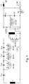
- FIG. 2 an alternative embodiment according to the invention is shown in which a parallel connection is used instead of the series connection.
- a secondary winding L1 is connected in series with a capacitor C_res1.
- system is laid as a primary conductor, an elongated line conductor, which is acted upon by a medium-frequency alternating current.
- the secondary winding L1 is provided inductively coupled to this primary conductor and arranged on a movable along the primary conductor vehicle.
- the vehicle is rail guided and laid the primary conductor along the rails.
- the capacitor C_res1 is a series connection of further capacitors (C_res2, C_res2, C_res3) connected in series, each of these capacitances (C_res2, C_res2, C_res3) a respective controllable semiconductor switch (AC-S2, AC-S3, AC-S4) connected in parallel , so that by opening the respective switch each parallel-connected capacitance is effective and ineffective by closing the switch.
- C_res1 is dimensioned such that by means of connecting or short-circuiting the capacitances (C_res2, C_res2, C_res3) it is possible to fine tune the resonance frequency or also the resonance quality.
- the output voltage U_AC1 of the series resonant circuit is fed to an autotransformer T, but a controllable semiconductor switch AC-S5 for shorting this output of the series resonant circuit is also provided.
- the inductance of the low voltage side of the autotransformer is substantially equal to the inductance of the secondary winding L1 of the series tuned circuit.
- the fine adjustment is carried out, so that the phase position and optionally also the resonance quality is performed as close as possible to their optimum setpoint and thus the unloaded resonant circuit is adjusted as well as possible resonance frequency.
- the series resonant circuit feeds a voltage-increasing circuit arrangement, which here by way of example has a step-up converter, wherein the energy supplied thereto can be supplied controlled via the switch AC-S1, with a voltage Doppler circuit comprising the switch AC-S5.
- switch AC-S1 With switch AC-S1 open, energy flow is fed to the low-voltage side of autotransformer T whose output current is fed to a single-phase bridge rectifier. Between a bridge point of the rectifier and a bridge point of a series circuit of two capacitors C1 and C2, a further controllable switch AC-S1 is provided, so that the AC-S1 voltage value of the rectified voltage from the switching state of the switch AC-S1 depends. In this case, the series connection of two capacitors C1 and C2 is supplied from the output side of the single-phase bridge rectifier.
- a consumer can be supplied, wherein a switch S6 is provided for connecting or disconnecting the power provided for the consumer I_DC.
- the current supplied to the consumer I_DC is passed through an inductor L2 and thus further smoothed. This current I_DC is detected and can be used as an input value, in particular actual value, of a controller.
- the rectified and smoothed output voltage UZ is also detected and can also be used as input value, in particular actual value, of a regulator.
- an up-converting operation can be carried out so that a higher voltage is available at the output side of the autotransformer than at the input side, that is to say the short-circuitable side by means of the switch AC-S1.
- the clock period of the clocked signal or, for example, the pulse width ratio of a pulse width modulated signal for driving the switch AC-S1 can be used as a manipulated variable of the controller.
- the switches are designed as controllable semiconductor switches, a simple and fast switching by means of a control electronics is possible.
- the switches (AC-S2, AC-S3, AC-S4) are operated in a clocked manner, in particular actuated at a suitably selected phase angle. In this way, depending on the phase angle, various intermediate values of effectively effective capacitances in the resonant circuit are effectively feasible.
- a suitable control it is possible to optimize the inductively transmitted power even during the loaded operation of the oscillatory circuit.
- the invention makes it possible to use a series resonant circuit, wherein the winding voltages occurring in the secondary inductance L1 are relatively small. Because despite the small Wickiungstapen and thus the increased safety for the secondary inductance and despite the possibly weak inductive coupling of the secondary inductance to the primary conductor is a sufficiently high voltage available to the consumer available, because the autotransformer is operated in boost converter operation and also by means of the switch AC- S5 a voltage doubling is achievable. Switching from the peak rectification of the single-phase bridge rectifier to the peak-to-peak rectification is enabled by means of the switch AC-S5.
- the rectified voltage is equal to the maximum amplitude of the AC current at the input side of the rectifier when the output side of the rectifier is unloaded.
- the rectified voltage is equal to twice the maximum amplitude of the AC on the input side of the rectifier when the output side of the rectifier is unloaded.
- the secondary inductance thus has a low number of turns. In this way, the inductive reaction of the secondary part on the primary conductor can be reduced.
Landscapes
- Engineering & Computer Science (AREA)
- Computer Networks & Wireless Communication (AREA)
- Power Engineering (AREA)
- Dc-Dc Converters (AREA)
- Generation Of Surge Voltage And Current (AREA)
- Rectifiers (AREA)
Claims (9)
- Dispositif de transmission d'énergie par induction à un consommateur électrique, dans lequel un enroulement secondaire (L1) est couplé par induction à un conducteur primaire, un ensemble de condensateurs (C_res2, C_res3, C_res4) étant connecté à l'enroulement secondaire (L1) pour former un circuit oscillant,
lequel circuit oscillant alimente un dispositif convertisseur élévateur avec dispositif redresseur et constitué d'un autotransformateur (T) et d'un commutateur commandable (AC-S1), dont la tension de sortie alimente un consommateur,
dans lequel- soit l'ensemble de condensateurs (C_res2, C_res3, C_res4) est réalisé sous la forme d'un couplage en série des condensateurs (C_res2, C_res3, C_res4), les condensateurs (C_res2, C_res3, C_res4) pouvant être court-circuités par un commutateur à semi-conducteurs commandable (AC-S2, AC-S3, AC-S4) respectivement associé, un commutateur commandable (AC-S1) étant connecté en parallèle avec le côté entrée de l'autotransformateur (T),- soit l'ensemble de condensateurs (C_res2, C_res3, C_res4) est réalisé sous la forme d'un couplage en parallèle des condensateurs (C_res2, C_res3, C_res4), les condensateurs (C_res2, C_res3, C_res4) pouvant être séparés par un commutateur à semi-conducteurs commandable (AC-S21, AC_S22, AC-S31, AC_S32, AC-S41, AC_S42) couplé en série respectivement associé, un commutateur commandable (AC-S1) étant connecté en série avec le côté entrée de l'autotransformateur (T) - Dispositif selon la revendication 1,
caractérisé en ce
qu'au côté secondaire de l'autotransformateur (T) est connecté un dispositif redresseur à partir duquel, par l'intermédiaire de moyens de lissage (C1, C2), un consommateur peut être alimenté. - Dispositif selon au moins l'une des revendications précédentes,
caractérisé en ce
que le commutateur commandable (AC-S1) est connecté en parallèle ou en série au côté entrée de l'autotransformateur (T), de sorte que, par commande cadencée de ce commutateur (AC-S1), la tension de sortie est réglable à une valeur de consigne, en particulier le signal de commande, en particulier sa fréquence et/ou son rapport de modulation de largeur d'impulsions, étant la grandeur réglante d'un régulateur auquel la valeur de tension de sortie détectée est amenée en tant que valeur réelle. - Dispositif selon la revendication 2,
caractérisé en ce
que le dispositif redresseur est commutable entre un redressement de valeur de crête et un redressement de valeur crête-crête, donc en particulier présente un circuit doubleur de tension. - Dispositif selon la revendication 2,
caractérisé en ce
que le dispositif redresseur présente un redresseur en demi-pont. - Dispositif selon la revendication 5,
caractérisé en ce
qu'un couplage en série de condensateurs (C1, C2) est connecté, en particulier connecté en parallèle, au dispositif redresseur côté sortie, un commutateur (AC-S5) étant disposé entre un demi-pont du dispositif redresseur et un noeud de connexion entre les condensateurs (C1, C2) de telle manière que la position de commutation de ce commutateur permette d'exercer une influence sur la tension de sortie. - Dispositif selon la revendication 6,
caractérisé en ce
qu'il est possible de commander le dispositif redresseur, en particulier le commutateur (AC-S5) entre le demi-pont du dispositif redresseur et le noeud de connexion, de façon cadencée, de telle manière que la tension de sortie du dispositif redresseur soit réglable à sa valeur de consigne,
et/ou
qu'il est possible de commander le courant d'entrée à l'autotransformateur (T) par le commutateur commandable (AC-S1) de façon cadencée, de telle manière que la tension de sortie du dispositif redresseur soit réglable à sa valeur de consigne. - Dispositif selon au moins l'une des revendications précédentes,
caractérisé en ce
qu'au moins un des condensateurs (C_res2, C_res3, C_res4) peut être connecté ou déconnecté au moyen d'un commutateur à semi-conducteurs commandable associé, donc en particulier rendu actif ou inactif pour le circuit oscillant,
en particulier pour accorder la fréquence de résonance du circuit oscillant à une fréquence de consigne, en particulier à une fréquence du courant appliqué dans le conducteur primaire. - Dispositif selon au moins l'une des revendications précédentes,
caractérisé en ce
que le circuit oscillant est un circuit oscillant parallèle ou un circuit oscillant série.
Priority Applications (1)
| Application Number | Priority Date | Filing Date | Title |
|---|---|---|---|
| EP13000391.6A EP2605361B1 (fr) | 2010-05-20 | 2011-04-21 | Agencement et procédé de fonctionnement d'un agencement destinés à la transmission d'énergie inductive vers un consommateur électrique |
Applications Claiming Priority (2)
| Application Number | Priority Date | Filing Date | Title |
|---|---|---|---|
| DE102010022122.8A DE102010022122B4 (de) | 2010-05-20 | 2010-05-20 | Anordnung und Verfahren zum Betreiben einer Anordnung zur induktiven Energieübertragung an einen elektrischen Verbraucher |
| PCT/EP2011/002042 WO2011144290A2 (fr) | 2010-05-20 | 2011-04-21 | Dispositif et procédé pour faire fonctionner un dispositif de transmission inductive d'énergie à un récepteur électrique |
Related Child Applications (3)
| Application Number | Title | Priority Date | Filing Date |
|---|---|---|---|
| EP13000391.6A Division EP2605361B1 (fr) | 2010-05-20 | 2011-04-21 | Agencement et procédé de fonctionnement d'un agencement destinés à la transmission d'énergie inductive vers un consommateur électrique |
| EP13000391.6A Division-Into EP2605361B1 (fr) | 2010-05-20 | 2011-04-21 | Agencement et procédé de fonctionnement d'un agencement destinés à la transmission d'énergie inductive vers un consommateur électrique |
| EP13000391.6 Division-Into | 2013-01-28 |
Publications (2)
| Publication Number | Publication Date |
|---|---|
| EP2572427A2 EP2572427A2 (fr) | 2013-03-27 |
| EP2572427B1 true EP2572427B1 (fr) | 2017-03-01 |
Family
ID=44626217
Family Applications (2)
| Application Number | Title | Priority Date | Filing Date |
|---|---|---|---|
| EP11718289.9A Active EP2572427B1 (fr) | 2010-05-20 | 2011-04-21 | Dispositif et procédé pour faire fonctionner un dispositif de transmission inductive d'énergie à un récepteur électrique |
| EP13000391.6A Active EP2605361B1 (fr) | 2010-05-20 | 2011-04-21 | Agencement et procédé de fonctionnement d'un agencement destinés à la transmission d'énergie inductive vers un consommateur électrique |
Family Applications After (1)
| Application Number | Title | Priority Date | Filing Date |
|---|---|---|---|
| EP13000391.6A Active EP2605361B1 (fr) | 2010-05-20 | 2011-04-21 | Agencement et procédé de fonctionnement d'un agencement destinés à la transmission d'énergie inductive vers un consommateur électrique |
Country Status (3)
| Country | Link |
|---|---|
| EP (2) | EP2572427B1 (fr) |
| DE (1) | DE102010022122B4 (fr) |
| WO (1) | WO2011144290A2 (fr) |
Families Citing this family (1)
| Publication number | Priority date | Publication date | Assignee | Title |
|---|---|---|---|---|
| EP2808196A1 (fr) | 2013-05-29 | 2014-12-03 | Brusa Elektronik AG | Elément de transmission |
Family Cites Families (18)
| Publication number | Priority date | Publication date | Assignee | Title |
|---|---|---|---|---|
| DE3305224A1 (de) | 1983-02-16 | 1984-08-16 | Bbc Brown Boveri & Cie | Bord-batterieladegeraet |
| DE4112907C1 (en) | 1991-04-19 | 1992-04-30 | Siemens Nixdorf Informationssysteme Ag, 4790 Paderborn, De | Mains-connected power supply circuit - has voltage doubler formed in two symmetrical circuit halves, and input voltage changeover switch for 115 or 230 volt operation |
| ES2163409T3 (es) * | 1992-05-10 | 2002-02-01 | Auckland Uniservices Ltd | Sistema de distribucion de energia desprovisto de contactos. |
| CH684722A5 (de) * | 1992-05-26 | 1994-11-30 | Siemens Ag Albis | Schaltungsanordnung zur Ankopplung einer Sendeeinheit an eine Uebertragungsleitung. |
| JP2674451B2 (ja) * | 1992-10-30 | 1997-11-12 | 株式会社島津製作所 | X線高電圧装置 |
| NO301917B1 (no) * | 1995-02-01 | 1997-12-22 | Fieldbus International As | Vekselström/likespennings-omformer |
| DE19602316C1 (de) | 1996-01-23 | 1997-06-19 | Siemens Ag | Vorrichtung zum Übertragen von Daten oder Energie |
| DE19621076C2 (de) | 1996-05-24 | 2001-06-28 | Siemens Ag | Vorrichtung und Verfahren zum kontaktlosen Übertragen von Energie oder Daten |
| DE19755250A1 (de) | 1997-12-12 | 1999-07-01 | Philips Patentverwaltung | Schaltungsanordnung zum Einstellen der Resonanzfrequenz |
| BR9907351A (pt) | 1999-12-22 | 2001-08-07 | Ericsson Telecomunicacoees S A | Método e circuito de controle para retificador do tipo elevador trifásico de três nìveis |
| JP3730087B2 (ja) * | 2000-06-13 | 2005-12-21 | 朝日松下電工株式会社 | 放電灯点灯装置 |
| DE102005005812A1 (de) | 2005-02-09 | 2006-08-17 | Atmel Germany Gmbh | Schaltungsanordnung und Verfahren zur Spannungsversorgung eines Transponders |
| JP2008005685A (ja) | 2006-06-20 | 2008-01-10 | Toshiaki Yanai | Dc−dcコンバータ |
| DE102007033654B4 (de) | 2006-09-20 | 2019-08-01 | Sew-Eurodrive Gmbh & Co Kg | System mit Wagen und Basiseinheiten |
| JP2008104295A (ja) | 2006-10-19 | 2008-05-01 | Voltex:Kk | 非接触電源装置 |
| US8855554B2 (en) * | 2008-03-05 | 2014-10-07 | Qualcomm Incorporated | Packaging and details of a wireless power device |
| US9178387B2 (en) | 2008-05-13 | 2015-11-03 | Qualcomm Incorporated | Receive antenna for wireless power transfer |
| US8461719B2 (en) * | 2008-09-27 | 2013-06-11 | Witricity Corporation | Wireless energy transfer systems |
-
2010
- 2010-05-20 DE DE102010022122.8A patent/DE102010022122B4/de active Active
-
2011
- 2011-04-21 WO PCT/EP2011/002042 patent/WO2011144290A2/fr active Application Filing
- 2011-04-21 EP EP11718289.9A patent/EP2572427B1/fr active Active
- 2011-04-21 EP EP13000391.6A patent/EP2605361B1/fr active Active
Also Published As
| Publication number | Publication date |
|---|---|
| EP2605361A2 (fr) | 2013-06-19 |
| EP2605361B1 (fr) | 2022-06-15 |
| WO2011144290A3 (fr) | 2012-05-10 |
| WO2011144290A2 (fr) | 2011-11-24 |
| DE102010022122A1 (de) | 2011-11-24 |
| DE102010022122B4 (de) | 2021-08-05 |
| EP2572427A2 (fr) | 2013-03-27 |
| EP2605361A3 (fr) | 2018-02-14 |
Similar Documents
| Publication | Publication Date | Title |
|---|---|---|
| EP2996235A1 (fr) | Convertisseur cc/cc | |
| EP2999079B1 (fr) | Systeme et procede de fonctionnement d'un systeme destine a la transmission d'energie inductive vers un consommateur electrique | |
| WO2015063683A1 (fr) | Procédé de réglage de l'énergie transmise entre des résonateurs d'un système destiné à la transmission d'énergie sans contact, et ensemble résonateur | |
| DE10020357A1 (de) | DC-DC-Konverter | |
| EP3091636A1 (fr) | Une procédure de la compensation adaptive pour un circuit résonant | |
| WO2016071029A1 (fr) | Systeme de transmission, procédé et système pour véhicules | |
| WO2016055180A1 (fr) | Procédé et système de charge sans contact d'un objet fonctionnant sur batterie | |
| EP2357657B1 (fr) | Agencement inductif | |
| EP2223408A2 (fr) | Système de transfert d'énergie sans contact et procédé correspondant | |
| EP2572427B1 (fr) | Dispositif et procédé pour faire fonctionner un dispositif de transmission inductive d'énergie à un récepteur électrique | |
| DE4344709C2 (de) | Verfahren zur Umwandlung von unterschiedlich großen Gleich- oder Wechselspannungen in eine beliebig vorgegebene Spannung | |
| DE102012206801A1 (de) | Schaltung mit einer stromrichterschaltung und verfahren zur leistungsanpassung | |
| EP3539814B1 (fr) | Dispositif de charge pour véhicules automobiles à commande de circuit sur le côté récepteur | |
| EP2404357B1 (fr) | Système et procédé de transmission d'énergie sans contact | |
| DE102008024602B4 (de) | Schaltungsanordnung und deren Verwendung | |
| WO2023041229A1 (fr) | Système de transmission d'énergie sans contact d'un conducteur primaire à une partie mobile | |
| WO2018029114A1 (fr) | Système et procédé de transmission d'énergie par induction | |
| DE102015009073B4 (de) | Anordnung zur induktiven Übertragung elektrischer Energie von einem stationär angeordneten Primärleiter an eine relativ dazu bewegbare Vorrichtung und Verfahren zum Betreiben der Anordnung | |
| DE102021132237A1 (de) | Ladegerät zur induktiven Energieübertragung, Verfahren zum Betrieb eines Ladegerätes, Ladesystem | |
| EP3221180A1 (fr) | Système de transmission de puissance électrique par induction | |
| DE10215840A1 (de) | NOT-AUS-System für induktiv versorgte Verbraucher | |
| DE10304505A1 (de) | Verfahren zur Speisung eines Induktionsofens oder Induktors |
Legal Events
| Date | Code | Title | Description |
|---|---|---|---|
| PUAI | Public reference made under article 153(3) epc to a published international application that has entered the european phase |
Free format text: ORIGINAL CODE: 0009012 |
|
| 17P | Request for examination filed |
Effective date: 20121220 |
|
| AK | Designated contracting states |
Kind code of ref document: A2 Designated state(s): AL AT BE BG CH CY CZ DE DK EE ES FI FR GB GR HR HU IE IS IT LI LT LU LV MC MK MT NL NO PL PT RO RS SE SI SK SM TR |
|
| DAX | Request for extension of the european patent (deleted) | ||
| 17Q | First examination report despatched |
Effective date: 20150508 |
|
| GRAP | Despatch of communication of intention to grant a patent |
Free format text: ORIGINAL CODE: EPIDOSNIGR1 |
|
| INTG | Intention to grant announced |
Effective date: 20161017 |
|
| STAA | Information on the status of an ep patent application or granted ep patent |
Free format text: STATUS: GRANT OF PATENT IS INTENDED |
|
| GRAS | Grant fee paid |
Free format text: ORIGINAL CODE: EPIDOSNIGR3 |
|
| GRAA | (expected) grant |
Free format text: ORIGINAL CODE: 0009210 |
|
| STAA | Information on the status of an ep patent application or granted ep patent |
Free format text: STATUS: THE PATENT HAS BEEN GRANTED |
|
| AK | Designated contracting states |
Kind code of ref document: B1 Designated state(s): AL AT BE BG CH CY CZ DE DK EE ES FI FR GB GR HR HU IE IS IT LI LT LU LV MC MK MT NL NO PL PT RO RS SE SI SK SM TR |
|
| REG | Reference to a national code |
Ref country code: GB Ref legal event code: FG4D Free format text: NOT ENGLISH |
|
| REG | Reference to a national code |
Ref country code: CH Ref legal event code: EP Ref country code: AT Ref legal event code: REF Ref document number: 872367 Country of ref document: AT Kind code of ref document: T Effective date: 20170315 |
|
| REG | Reference to a national code |
Ref country code: IE Ref legal event code: FG4D Free format text: LANGUAGE OF EP DOCUMENT: GERMAN |
|
| REG | Reference to a national code |
Ref country code: FR Ref legal event code: PLFP Year of fee payment: 7 |
|
| REG | Reference to a national code |
Ref country code: DE Ref legal event code: R096 Ref document number: 502011011720 Country of ref document: DE |
|
| REG | Reference to a national code |
Ref country code: NL Ref legal event code: MP Effective date: 20170301 |
|
| REG | Reference to a national code |
Ref country code: LT Ref legal event code: MG4D |
|
| PG25 | Lapsed in a contracting state [announced via postgrant information from national office to epo] |
Ref country code: NO Free format text: LAPSE BECAUSE OF FAILURE TO SUBMIT A TRANSLATION OF THE DESCRIPTION OR TO PAY THE FEE WITHIN THE PRESCRIBED TIME-LIMIT Effective date: 20170601 Ref country code: GR Free format text: LAPSE BECAUSE OF FAILURE TO SUBMIT A TRANSLATION OF THE DESCRIPTION OR TO PAY THE FEE WITHIN THE PRESCRIBED TIME-LIMIT Effective date: 20170602 Ref country code: HR Free format text: LAPSE BECAUSE OF FAILURE TO SUBMIT A TRANSLATION OF THE DESCRIPTION OR TO PAY THE FEE WITHIN THE PRESCRIBED TIME-LIMIT Effective date: 20170301 Ref country code: LT Free format text: LAPSE BECAUSE OF FAILURE TO SUBMIT A TRANSLATION OF THE DESCRIPTION OR TO PAY THE FEE WITHIN THE PRESCRIBED TIME-LIMIT Effective date: 20170301 Ref country code: FI Free format text: LAPSE BECAUSE OF FAILURE TO SUBMIT A TRANSLATION OF THE DESCRIPTION OR TO PAY THE FEE WITHIN THE PRESCRIBED TIME-LIMIT Effective date: 20170301 |
|
| PG25 | Lapsed in a contracting state [announced via postgrant information from national office to epo] |
Ref country code: LV Free format text: LAPSE BECAUSE OF FAILURE TO SUBMIT A TRANSLATION OF THE DESCRIPTION OR TO PAY THE FEE WITHIN THE PRESCRIBED TIME-LIMIT Effective date: 20170301 Ref country code: ES Free format text: LAPSE BECAUSE OF FAILURE TO SUBMIT A TRANSLATION OF THE DESCRIPTION OR TO PAY THE FEE WITHIN THE PRESCRIBED TIME-LIMIT Effective date: 20170301 Ref country code: SE Free format text: LAPSE BECAUSE OF FAILURE TO SUBMIT A TRANSLATION OF THE DESCRIPTION OR TO PAY THE FEE WITHIN THE PRESCRIBED TIME-LIMIT Effective date: 20170301 Ref country code: BG Free format text: LAPSE BECAUSE OF FAILURE TO SUBMIT A TRANSLATION OF THE DESCRIPTION OR TO PAY THE FEE WITHIN THE PRESCRIBED TIME-LIMIT Effective date: 20170601 Ref country code: RS Free format text: LAPSE BECAUSE OF FAILURE TO SUBMIT A TRANSLATION OF THE DESCRIPTION OR TO PAY THE FEE WITHIN THE PRESCRIBED TIME-LIMIT Effective date: 20170301 |
|
| PG25 | Lapsed in a contracting state [announced via postgrant information from national office to epo] |
Ref country code: NL Free format text: LAPSE BECAUSE OF FAILURE TO SUBMIT A TRANSLATION OF THE DESCRIPTION OR TO PAY THE FEE WITHIN THE PRESCRIBED TIME-LIMIT Effective date: 20170301 |
|
| PG25 | Lapsed in a contracting state [announced via postgrant information from national office to epo] |
Ref country code: CZ Free format text: LAPSE BECAUSE OF FAILURE TO SUBMIT A TRANSLATION OF THE DESCRIPTION OR TO PAY THE FEE WITHIN THE PRESCRIBED TIME-LIMIT Effective date: 20170301 Ref country code: IT Free format text: LAPSE BECAUSE OF FAILURE TO SUBMIT A TRANSLATION OF THE DESCRIPTION OR TO PAY THE FEE WITHIN THE PRESCRIBED TIME-LIMIT Effective date: 20170301 Ref country code: RO Free format text: LAPSE BECAUSE OF FAILURE TO SUBMIT A TRANSLATION OF THE DESCRIPTION OR TO PAY THE FEE WITHIN THE PRESCRIBED TIME-LIMIT Effective date: 20170301 Ref country code: EE Free format text: LAPSE BECAUSE OF FAILURE TO SUBMIT A TRANSLATION OF THE DESCRIPTION OR TO PAY THE FEE WITHIN THE PRESCRIBED TIME-LIMIT Effective date: 20170301 Ref country code: SK Free format text: LAPSE BECAUSE OF FAILURE TO SUBMIT A TRANSLATION OF THE DESCRIPTION OR TO PAY THE FEE WITHIN THE PRESCRIBED TIME-LIMIT Effective date: 20170301 |
|
| PG25 | Lapsed in a contracting state [announced via postgrant information from national office to epo] |
Ref country code: PL Free format text: LAPSE BECAUSE OF FAILURE TO SUBMIT A TRANSLATION OF THE DESCRIPTION OR TO PAY THE FEE WITHIN THE PRESCRIBED TIME-LIMIT Effective date: 20170301 Ref country code: IS Free format text: LAPSE BECAUSE OF FAILURE TO SUBMIT A TRANSLATION OF THE DESCRIPTION OR TO PAY THE FEE WITHIN THE PRESCRIBED TIME-LIMIT Effective date: 20170701 Ref country code: SM Free format text: LAPSE BECAUSE OF FAILURE TO SUBMIT A TRANSLATION OF THE DESCRIPTION OR TO PAY THE FEE WITHIN THE PRESCRIBED TIME-LIMIT Effective date: 20170301 Ref country code: PT Free format text: LAPSE BECAUSE OF FAILURE TO SUBMIT A TRANSLATION OF THE DESCRIPTION OR TO PAY THE FEE WITHIN THE PRESCRIBED TIME-LIMIT Effective date: 20170703 |
|
| REG | Reference to a national code |
Ref country code: CH Ref legal event code: PL |
|
| REG | Reference to a national code |
Ref country code: DE Ref legal event code: R097 Ref document number: 502011011720 Country of ref document: DE |
|
| PLBE | No opposition filed within time limit |
Free format text: ORIGINAL CODE: 0009261 |
|
| STAA | Information on the status of an ep patent application or granted ep patent |
Free format text: STATUS: NO OPPOSITION FILED WITHIN TIME LIMIT |
|
| REG | Reference to a national code |
Ref country code: IE Ref legal event code: MM4A |
|
| PG25 | Lapsed in a contracting state [announced via postgrant information from national office to epo] |
Ref country code: DK Free format text: LAPSE BECAUSE OF FAILURE TO SUBMIT A TRANSLATION OF THE DESCRIPTION OR TO PAY THE FEE WITHIN THE PRESCRIBED TIME-LIMIT Effective date: 20170301 Ref country code: MC Free format text: LAPSE BECAUSE OF FAILURE TO SUBMIT A TRANSLATION OF THE DESCRIPTION OR TO PAY THE FEE WITHIN THE PRESCRIBED TIME-LIMIT Effective date: 20170301 |
|
| 26N | No opposition filed |
Effective date: 20171204 |
|
| PG25 | Lapsed in a contracting state [announced via postgrant information from national office to epo] |
Ref country code: LU Free format text: LAPSE BECAUSE OF NON-PAYMENT OF DUE FEES Effective date: 20170421 Ref country code: LI Free format text: LAPSE BECAUSE OF NON-PAYMENT OF DUE FEES Effective date: 20170430 Ref country code: CH Free format text: LAPSE BECAUSE OF NON-PAYMENT OF DUE FEES Effective date: 20170430 Ref country code: SI Free format text: LAPSE BECAUSE OF FAILURE TO SUBMIT A TRANSLATION OF THE DESCRIPTION OR TO PAY THE FEE WITHIN THE PRESCRIBED TIME-LIMIT Effective date: 20170301 |
|
| REG | Reference to a national code |
Ref country code: FR Ref legal event code: PLFP Year of fee payment: 8 |
|
| REG | Reference to a national code |
Ref country code: BE Ref legal event code: MM Effective date: 20170430 |
|
| PG25 | Lapsed in a contracting state [announced via postgrant information from national office to epo] |
Ref country code: IE Free format text: LAPSE BECAUSE OF NON-PAYMENT OF DUE FEES Effective date: 20170421 |
|
| PG25 | Lapsed in a contracting state [announced via postgrant information from national office to epo] |
Ref country code: BE Free format text: LAPSE BECAUSE OF NON-PAYMENT OF DUE FEES Effective date: 20170430 |
|
| REG | Reference to a national code |
Ref country code: AT Ref legal event code: MM01 Ref document number: 872367 Country of ref document: AT Kind code of ref document: T Effective date: 20170421 |
|
| PG25 | Lapsed in a contracting state [announced via postgrant information from national office to epo] |
Ref country code: AT Free format text: LAPSE BECAUSE OF NON-PAYMENT OF DUE FEES Effective date: 20170421 |
|
| PG25 | Lapsed in a contracting state [announced via postgrant information from national office to epo] |
Ref country code: MT Free format text: LAPSE BECAUSE OF FAILURE TO SUBMIT A TRANSLATION OF THE DESCRIPTION OR TO PAY THE FEE WITHIN THE PRESCRIBED TIME-LIMIT Effective date: 20170301 |
|
| PG25 | Lapsed in a contracting state [announced via postgrant information from national office to epo] |
Ref country code: HU Free format text: LAPSE BECAUSE OF FAILURE TO SUBMIT A TRANSLATION OF THE DESCRIPTION OR TO PAY THE FEE WITHIN THE PRESCRIBED TIME-LIMIT; INVALID AB INITIO Effective date: 20110421 |
|
| PG25 | Lapsed in a contracting state [announced via postgrant information from national office to epo] |
Ref country code: CY Free format text: LAPSE BECAUSE OF NON-PAYMENT OF DUE FEES Effective date: 20170301 |
|
| PG25 | Lapsed in a contracting state [announced via postgrant information from national office to epo] |
Ref country code: MK Free format text: LAPSE BECAUSE OF FAILURE TO SUBMIT A TRANSLATION OF THE DESCRIPTION OR TO PAY THE FEE WITHIN THE PRESCRIBED TIME-LIMIT Effective date: 20170301 |
|
| PG25 | Lapsed in a contracting state [announced via postgrant information from national office to epo] |
Ref country code: TR Free format text: LAPSE BECAUSE OF FAILURE TO SUBMIT A TRANSLATION OF THE DESCRIPTION OR TO PAY THE FEE WITHIN THE PRESCRIBED TIME-LIMIT Effective date: 20170301 |
|
| PG25 | Lapsed in a contracting state [announced via postgrant information from national office to epo] |
Ref country code: AL Free format text: LAPSE BECAUSE OF FAILURE TO SUBMIT A TRANSLATION OF THE DESCRIPTION OR TO PAY THE FEE WITHIN THE PRESCRIBED TIME-LIMIT Effective date: 20170301 |
|
| PGFP | Annual fee paid to national office [announced via postgrant information from national office to epo] |
Ref country code: FR Payment date: 20230309 Year of fee payment: 13 |
|
| PGFP | Annual fee paid to national office [announced via postgrant information from national office to epo] |
Ref country code: DE Payment date: 20230430 Year of fee payment: 13 |
|
| PGFP | Annual fee paid to national office [announced via postgrant information from national office to epo] |
Ref country code: GB Payment date: 20240229 Year of fee payment: 14 |