EP2572389B1 - Production of electronic switching devices - Google Patents
Production of electronic switching devices Download PDFInfo
- Publication number
- EP2572389B1 EP2572389B1 EP11727666.7A EP11727666A EP2572389B1 EP 2572389 B1 EP2572389 B1 EP 2572389B1 EP 11727666 A EP11727666 A EP 11727666A EP 2572389 B1 EP2572389 B1 EP 2572389B1
- Authority
- EP
- European Patent Office
- Prior art keywords
- roller
- layer
- substrate
- liquid material
- thickness
- Prior art date
- Legal status (The legal status is an assumption and is not a legal conclusion. Google has not performed a legal analysis and makes no representation as to the accuracy of the status listed.)
- Not-in-force
Links
Images


Classifications
-
- H—ELECTRICITY
- H10—SEMICONDUCTOR DEVICES; ELECTRIC SOLID-STATE DEVICES NOT OTHERWISE PROVIDED FOR
- H10K—ORGANIC ELECTRIC SOLID-STATE DEVICES
- H10K71/00—Manufacture or treatment specially adapted for the organic devices covered by this subclass
- H10K71/10—Deposition of organic active material
- H10K71/12—Deposition of organic active material using liquid deposition, e.g. spin coating
- H10K71/13—Deposition of organic active material using liquid deposition, e.g. spin coating using printing techniques, e.g. ink-jet printing or screen printing
-
- H—ELECTRICITY
- H10—SEMICONDUCTOR DEVICES; ELECTRIC SOLID-STATE DEVICES NOT OTHERWISE PROVIDED FOR
- H10K—ORGANIC ELECTRIC SOLID-STATE DEVICES
- H10K10/00—Organic devices specially adapted for rectifying, amplifying, oscillating or switching; Organic capacitors or resistors having potential barriers
-
- H—ELECTRICITY
- H10—SEMICONDUCTOR DEVICES; ELECTRIC SOLID-STATE DEVICES NOT OTHERWISE PROVIDED FOR
- H10P—GENERIC PROCESSES OR APPARATUS FOR THE MANUFACTURE OR TREATMENT OF DEVICES COVERED BY CLASS H10
- H10P14/00—Formation of materials, e.g. in the shape of layers or pillars
- H10P14/20—Formation of materials, e.g. in the shape of layers or pillars of semiconductor materials
-
- H—ELECTRICITY
- H10—SEMICONDUCTOR DEVICES; ELECTRIC SOLID-STATE DEVICES NOT OTHERWISE PROVIDED FOR
- H10K—ORGANIC ELECTRIC SOLID-STATE DEVICES
- H10K99/00—Subject matter not provided for in other groups of this subclass
-
- H—ELECTRICITY
- H10—SEMICONDUCTOR DEVICES; ELECTRIC SOLID-STATE DEVICES NOT OTHERWISE PROVIDED FOR
- H10P—GENERIC PROCESSES OR APPARATUS FOR THE MANUFACTURE OR TREATMENT OF DEVICES COVERED BY CLASS H10
- H10P14/00—Formation of materials, e.g. in the shape of layers or pillars
- H10P14/60—Formation of materials, e.g. in the shape of layers or pillars of insulating materials
- H10P14/63—Formation of materials, e.g. in the shape of layers or pillars of insulating materials characterised by the formation processes
- H10P14/6326—Deposition processes
-
- H—ELECTRICITY
- H10—SEMICONDUCTOR DEVICES; ELECTRIC SOLID-STATE DEVICES NOT OTHERWISE PROVIDED FOR
- H10K—ORGANIC ELECTRIC SOLID-STATE DEVICES
- H10K10/00—Organic devices specially adapted for rectifying, amplifying, oscillating or switching; Organic capacitors or resistors having potential barriers
- H10K10/40—Organic transistors
- H10K10/46—Field-effect transistors, e.g. organic thin-film transistors [OTFT]
- H10K10/462—Insulated gate field-effect transistors [IGFETs]
- H10K10/464—Lateral top-gate IGFETs comprising only a single gate
-
- H—ELECTRICITY
- H10—SEMICONDUCTOR DEVICES; ELECTRIC SOLID-STATE DEVICES NOT OTHERWISE PROVIDED FOR
- H10K—ORGANIC ELECTRIC SOLID-STATE DEVICES
- H10K10/00—Organic devices specially adapted for rectifying, amplifying, oscillating or switching; Organic capacitors or resistors having potential barriers
- H10K10/40—Organic transistors
- H10K10/46—Field-effect transistors, e.g. organic thin-film transistors [OTFT]
- H10K10/462—Insulated gate field-effect transistors [IGFETs]
- H10K10/466—Lateral bottom-gate IGFETs comprising only a single gate
-
- H—ELECTRICITY
- H10—SEMICONDUCTOR DEVICES; ELECTRIC SOLID-STATE DEVICES NOT OTHERWISE PROVIDED FOR
- H10K—ORGANIC ELECTRIC SOLID-STATE DEVICES
- H10K71/00—Manufacture or treatment specially adapted for the organic devices covered by this subclass
- H10K71/851—Division of substrate
Definitions
- the present invention relates to the deposition of electronically functional organic layers of electronic switching devices. In one embodiment, it relates to the formation of a semiconductor channel and/or a gate dielectric layer in the production of an organic field effect transistor product.
- pixellated display devices typically comprise an active matrix array of organic thin-film field effect transistors (TFTs) for independent controlling the state of each pixel.
- TFTs organic thin-film field effect transistors
- Each TFT comprises an organic semiconductor channel between a pair of source and drain electrodes, and a gate electrode for controlling the conductivity of the semiconductor channel via an organic gate dielectric element.
- the production of large area display devices of the kind mentioned above typically comprises forming a continuous layer of an organic semiconductor material to form the semiconductor channels of the whole array of TFTs, and/or forming a continuous layer of an organic dielectric material to form the gate dielectric elements of the whole array of TFTs.
- the formation of such continuous organic layers is conventionally done by spin-coating, slit-coating, spray-coating, dip-coating or screen printing.
- DE102004046428 describes the production of an electronic component comprises preparing a substrate with a structured metallic layer in the form of a substrate strip wound onto a first roller, unwinding the strip from the roller, contacting the metallic layer with a solution containing an organic compound to form a mono-layer of organic compound on the metallic layer and rolling the strip onto a second roller.
- the present invention provides a method according to claim 1.
- the method further comprises selectively depositing said liquid material onto selected regions of said substrate to form a patterned layer in a single rotation of said first roller.
- the thickness non-uniformity of said patterned layer over the combined area of said patterned layer is less than about 7%.
- the substrate defines a plurality of patterned conductive layers in respective selected regions of the substrate, and said patterned layer of material provides a respective layer of said material over each of said patterned conductive layers.
- each of said patterned conductive layers defines a respective array of source-drain electrode pairs for a respective array of transistors, or a respective array of gate lines for a respective array of transistors.
- the rear edge of said material transferred from said first roller onto the substrate has a thickness substantially no greater than the average thickness of the remainder of the layer deposited onto the substrate.
- the tangential speed of the second roller is between about 2% and about 5% greater than the tangential speed of the first roller.
- the surface of the first roller defines a plurality of parallel grooves for receiving and holding said material; and further comprising cleaning the first roller by passing one or more cleaning solvents over the first roller in a direction perpendicular to said parallel grooves.
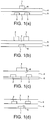
- FIGS 1(a) to 1(d) show two examples of TFT architectures: a top-gate structure and a bottom-gate structure.
- a TFT comprises source and drain electrodes 2, 3 connected by a semiconductor channel 7; and a gate electrode 1 separated from the semiconductor channel via a gate dielectric element 8.
- the conductivity of the semiconductor channel 7 can be controlled by adjusting the bias applied to the gate electrode 1.
- the semiconductor channel can be switched between essentially on (conducting) and off (nonconducting) states by switching the bias applied to the gate electrode between two levels.
- the semiconductor channel 7 and the dielectric element of the TFT shown is formed by a continuous layer of semiconductor material 5 and a continuous layer of dielectric material 4, respectively.
- the layers 4, 5 of semiconductor material and dielectric material are each formed of an organic polymeric material, and are deposited using the kind of apparatus shown in Figures 2 and 3 .
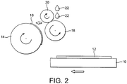
- the substrate 12 onto which a continuous layer of dielectric and/or semiconductor material is to be formed is mounted on a stage 10 which is itself mounted for linear movement in the direction shown by the arrow in Figure 2 .
- the substrate 12 comprises a continuous sheet 60 of device substrate material supported on a rigid glass carrier.
- the device substrate material 60 provides a plurality of device substrates for the same number of display device products.
- the plurality of device substrates are cut from the continuous sheet of device substrate material at a later stage of the production process.
- the regions of the device substrate material sheet 60 that later form the device substrates are designated by reference numerals 62 in Figure 6.
- Figure 6 shows a simple example where the device substrate material sheet provides two device substrates, but larger numbers are also possible and beneficial from the point of view of achieving an efficient production process.
- the continuous sheet of device substrate material 60 has already been subject to at least the following steps: the formation of a planarisation layer (not shown), and the formation in the device substrate regions 62 of a patterned metal layer (not shown) that defines the bottom conductive layer of the respective array of TFTs.
- the bottom conductive layer could be a layer that defines the source-drain electrode pairs and interconnect/signal lines (in the case of an array of top-gate TFTs of the kind shown in Figure 1(a) ) or a layer that defines an array of gate lines (in the case of an array of bottom-gate TFTs of the kind shown in Figure 1 (b) ).
- a TFT array is formed on each device substrate region 62 to form a backplane for a display device, and a respective pre-prepared frontplane including a display medium is laminated to each completed backplane.
- the above-mentioned cutting of the device substrate material takes place after lamination of the front planes to the backplanes.
- a cylinder roller 14 is provided on a surface thereof with a mat 16 configured to receive and hold in microrecesses liquid 22 to be deposited onto the substrate 12.
- microrecesses are only provided at those regions of the mat corresponding to the device substrate regions 62 mentioned above, so that only these selected sections of the mat hold liquid 22 to be deposited onto the substrate 12, and so that a set of layers are formed on the device substrate regions 62 substantially without any deposition of the liquid 22 on the areas of the substrate 12 between the device substrate regions 62.
- the set of layers that is so deposited is referred to below as a patterned layer, and this patterned layer is achieved without having to use a mask.
- the liquid 22 comprises a solution of the semiconductor or dielectric material in a solvent.
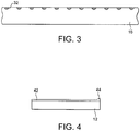
- the microrecesses 32 can, for example, take the form of an array of parallel microgrooves 32 or an array of micropores. With said microrecesses loaded with liquid 22 for deposition onto the substrate, cylinder roller 14 is rotated about a stationary axis as the stage is moved in the direction shown by the arrow in Figure 2 , such that the mat 16 is rolled under pressure over the surface of the substrate 12. This action forces the liquid 22 held in the microrecesses to be expelled from the microrecesses onto the surface of the substrate 12 to form continuous layers of the liquid on the device substrate region 62 of the substrate 12.
- the tangential speed of cylinder roller 14 during this process is the same as the linear speed of the stage 10 on which the substrate 12 is mounted.
- the stage 10 is then lowered by a small amount and moved back in the opposite direction to the starting position, in preparation for the deposition of a second layer of the other of the semiconductor and dielectric materials.
- One of the challenges of achieving the sufficient level of print quality for forming semiconductor and gate dielectric layers of a transistor by this kind of technique is avoiding dried particles of the semiconductor or gate dielectric material forming on the mat.
- the inventors have found that the use of (i) a solvent having a boiling point of no less than about 100°C and a vapour pressure greater than 17mmHg at 20°C, or (ii) a solvent having a boiling point of greater than 195°C (and any value of vapour pressure), can effectively avoid the formation of such dried particles on the mat.
- Suitable solvents having these properties include:
- the CAS numbers are Chemical Abstract Services registry numbers.
- the thickness uniformity of the patterned layer formed on the substrate 12 depends on the extent to which the mat 16 resists swelling by the solvent of the liquid 22. It has been found that it is possible to achieve a thickness non-uniformity of less than 7%, more particularly less than 5%, by using a solvent where the amount of swelling is no more than 30%, where the amount of swelling is defined by the percentage weight gain after soaking the mat for 24 hours in the solvent.
- the thickness non-uniformity of the deposited patterned layer is defined as the size of the variation in thickness of the deposited patterned layer after drying (e.g. the difference between the average thickness of the dried patterned layer and the minimum or maximum thickness of the dried patterned layer) expressed as a percentage of the average thickness of the deposited patterned layer.
- the average thickness and the minimum or maximum thickness of the deposited material after drying is comprising an equal number of thickness measurements for each of the device substrate regions 62, at uniformly spaced points of the respective device substrate regions 62.
- This good level of uniformity is achieved in this embodiment using a mat made of a material that is compatible with the solvent used to deposit the semiconductor or dielectric material, i.e. a solvent that passes the swelling test described above.
- solvents for organic semiconductor or dielectric materials in this embodiment include: diethylene glycol monoethyl ether acetate, 1-methyl-2-pyrrolidinone, alcohol based solvents, aromatic hydrocarbons and fluorinated based solvents (such as fluorocarbon solvents).
- the liquid 22 is loaded onto the mat using a second cylinder roller 18.
- a layer of the liquid 22 is formed on the surface of the second cylinder roller 18, and the liquid 22 is transferred from the second cylinder roller to the mat 16 by pushing the second cylinder roller 18 against the mat 16 and rotating both the cylinder rollers 16 and 18.
- rotating the two rollers 16 and 18 at the same tangential speed can produce what can be called a lip effect or edge effect at the rear edge of the resulting patterned layer on the substrate 12, i.e.
- the thickness of a rear edge portion 44 of the patterned layer 42 is greater than the average thickness of the remainder of the patterned layer 42.
- the rear edge portion of the patterned layer is the portion of the patterned layer 42 that is the last to be transferred from the cylinder roller 14 to the substrate 12 as the mat 16 is rolled over the substrate 12.
- excess thickness at the said rear edge portion of the patterned layer of material deposited from the cylinder roller 14 onto the substrate 12 can be substantially eliminated by rotating the two cylinder rollers 14 and 18 such that the tangential speed of the second cylinder roller 18 is about 2% to 5%, more particularly about 2.5% to 5%, greater than the tangential speed of the cylinder roller 14 during the process of transferring liquid from the second cylinder roller 18 to the mat 16.
- the first cylinder roller 14 is operated at a tangential speed of about 20m/s and the second cylinder roller 18 is operated at a tangential speed of about 20.5m/s.
- the third cylinder roller 20 functions to improve the uniformity of the coating of liquid 22 on the second cylinder roller 18.
- the mat 16 may be necessary to first condition the mat 16 by performing one or more dummy runs involving the transfer of the said material from the second cylinder roller 18 onto the first cylinder roller 14 and then onto a substrate on stage 10, which substrate could be the same kind of substrate 12 as described above (which would afterwards be discarded or recycled), or a dummy substrate without the features necessary to produce a TFT array.
- the dummy runs can serve to remove undesirable particles from the mat 16, which particles could otherwise be a cause of poor uniformity of thickness in the deposited layers.
- semiconductor materials for the semiconductor channels 7 include: polythiophenes such as poly 3-hexylthiophene (P3HT); poly 2,5-thienylene vinylene; poly p-phenylenevinylene (PPV); polyfluorene materials such as poly(9,9-dioctylfluorene, poly(9,9-dioctylfluorene-co-benzothiadiazole, poly(9,9-dialkylflourne-co-bithiophene, poly(9,9-dioctylfluorene-co-bis-N,N'-(4-butylphenyl)diphenylamine), poly(9,9-dioctylfluorene-co-bis-N,N'-(4-butylphenyl)-bis-N,N'-phenyl-1,4-phenylenediamine); polydiacetylene; pentacene and pent
- dielectric materials for the gate dielectric elements 8 include polystyrene (PS), polyvinylphenols, polymethylmethacrylates (PMMA), Teflon® AF fluoropolymers available from Dupont, Cytop® fluoropolymers available from Asahi Glass Chemicals, SU-8 epoxy resins, poyisobutylenes, polynorbornenes, and PS-PMMA copolymers.
- PS polystyrene
- PMMA polymethylmethacrylates
- Teflon® AF fluoropolymers available from Dupont
- Cytop® fluoropolymers available from Asahi Glass Chemicals
- SU-8 epoxy resins poyisobutylenes
- polynorbornenes polynorbornenes
- the microrecesses 32 can take the form of an array of parallel microgrooves 32, as illustrated in Figure 5 .
- Cleaning of the mat comprises two wiping steps using different solvents, a first, relatively high boiling point solvent for the main cleaning, and a second, relatively low boiling point solvent for aiding drying of the mat.
- the first solvent has a higher boiling point that the second solvent.
- Cleaning of the mat is done when the production process is to be stopped for a significant period of time, and when again resuming the production process.
- cleaning is best achieved by passing the cleaning solvents over the mat in a direction perpendicular to the microgrooves 32. Cleaning of the mat is carried out manually passing a cleanroom cloth soaked in solvent in a direction perpendicular to the microgrooves 32. For example, at least three cleaning passes are done with the first high boiling point solvent followed by at least three cleaning passes with the low boiling point solvent.
- the above-described technique can be used in combination with other deposition techniques.
- it can be used to deposit an organic polymeric semiconductor layer and/or organic dielectric layer in a device including a gate dielectric layer or additional gate dielectric layer of a dielectric bilayer structure deposited by a vapour deposition technique.
Landscapes
- Engineering & Computer Science (AREA)
- Manufacturing & Machinery (AREA)
- Thin Film Transistor (AREA)
- Liquid Deposition Of Substances Of Which Semiconductor Devices Are Composed (AREA)
- Formation Of Insulating Films (AREA)
Description
- The present invention relates to the deposition of electronically functional organic layers of electronic switching devices. In one embodiment, it relates to the formation of a semiconductor channel and/or a gate dielectric layer in the production of an organic field effect transistor product.
- Many organic electronic devices comprise an array of organic field effect transistors. For example, pixellated display devices typically comprise an active matrix array of organic thin-film field effect transistors (TFTs) for independent controlling the state of each pixel. Each TFT comprises an organic semiconductor channel between a pair of source and drain electrodes, and a gate electrode for controlling the conductivity of the semiconductor channel via an organic gate dielectric element.
- The production of large area display devices of the kind mentioned above typically comprises forming a continuous layer of an organic semiconductor material to form the semiconductor channels of the whole array of TFTs, and/or forming a continuous layer of an organic dielectric material to form the gate dielectric elements of the whole array of TFTs. The formation of such continuous organic layers is conventionally done by spin-coating, slit-coating, spray-coating, dip-coating or screen printing.
- It is an aim of the present invention to provide a new technique by which a continuous layer of organic semiconductor material and/or organic dielectric material having the necessary properties for forming these electronically functionally elements of electronic switching devices can be consistently and reliably formed.
-
DE102004046428 describes the production of an electronic component comprises preparing a substrate with a structured metallic layer in the form of a substrate strip wound onto a first roller, unwinding the strip from the roller, contacting the metallic layer with a solution containing an organic compound to form a mono-layer of organic compound on the metallic layer and rolling the strip onto a second roller. - The present invention provides a method according to
claim 1. - In one embodiment, the method further comprises selectively depositing said liquid material onto selected regions of said substrate to form a patterned layer in a single rotation of said first roller.
- In one embodiment, the thickness non-uniformity of said patterned layer over the combined area of said patterned layer is less than about 7%.
- In one embodiment, the substrate defines a plurality of patterned conductive layers in respective selected regions of the substrate, and said patterned layer of material provides a respective layer of said material over each of said patterned conductive layers.
- In one embodiment, each of said patterned conductive layers defines a respective array of source-drain electrode pairs for a respective array of transistors, or a respective array of gate lines for a respective array of transistors.
- By controlling the tangential speed of the second roller, the rear edge of said material transferred from said first roller onto the substrate has a thickness substantially no greater than the average thickness of the remainder of the layer deposited onto the substrate.
- In one embodiment, the tangential speed of the second roller is between about 2% and about 5% greater than the tangential speed of the first roller.
- In one embodiment, the surface of the first roller defines a plurality of parallel grooves for receiving and holding said material; and further comprising cleaning the first roller by passing one or more cleaning solvents over the first roller in a direction perpendicular to said parallel grooves.
- An embodiment of the present invention shall be described in detail hereunder, by way of example only, with reference to the accompanying drawings in which:
-
Figures 1(a) to Figures 1(d) illustrate two kinds of TFT architectures in which a continuous layer of semiconductor material forms the semiconductor channels of an array of TFTs and a continuous layer of dielectric material forms the gate dielectric elements of an array of TFTs; -
Figure 2 illustrates apparatus for use in a method according to an embodiment of the present invention; -
Figure 3 illustrates in more detail a mat used in the apparatus shown inFigure 2 ; -
Figure 4 illustrates a problem solved by a method according to an embodiment of the present invention; -
Figure 5 illustrates an aspect of an embodiment of the present invention; -
Figure 6 illustrates accordance substrate used in an embodiment of the present invention; and -
Figure 7 illustrates a mat for depositing a patterned layer of material in accordance with an embodiment of the present invention. -
Figures 1(a) to 1(d) show two examples of TFT architectures: a top-gate structure and a bottom-gate structure. In both architectures, a TFT comprises source anddrain electrodes semiconductor channel 7; and agate electrode 1 separated from the semiconductor channel via a gatedielectric element 8. The conductivity of thesemiconductor channel 7 can be controlled by adjusting the bias applied to thegate electrode 1. For example, the semiconductor channel can be switched between essentially on (conducting) and off (nonconducting) states by switching the bias applied to the gate electrode between two levels. In each of the architectures, thesemiconductor channel 7 and the dielectric element of the TFT shown (and also other TFTs in the same array (not shown) is formed by a continuous layer ofsemiconductor material 5 and a continuous layer ofdielectric material 4, respectively. - In this embodiment of the invention, the
layers Figures 2 and3 . - The
substrate 12 onto which a continuous layer of dielectric and/or semiconductor material is to be formed is mounted on astage 10 which is itself mounted for linear movement in the direction shown by the arrow inFigure 2 . With reference toFigure 6 , thesubstrate 12 comprises acontinuous sheet 60 of device substrate material supported on a rigid glass carrier. Thedevice substrate material 60 provides a plurality of device substrates for the same number of display device products. The plurality of device substrates are cut from the continuous sheet of device substrate material at a later stage of the production process. - The regions of the device
substrate material sheet 60 that later form the device substrates are designated byreference numerals 62 inFigure 6. Figure 6 shows a simple example where the device substrate material sheet provides two device substrates, but larger numbers are also possible and beneficial from the point of view of achieving an efficient production process. The continuous sheet ofdevice substrate material 60 has already been subject to at least the following steps: the formation of a planarisation layer (not shown), and the formation in thedevice substrate regions 62 of a patterned metal layer (not shown) that defines the bottom conductive layer of the respective array of TFTs. The bottom conductive layer could be a layer that defines the source-drain electrode pairs and interconnect/signal lines (in the case of an array of top-gate TFTs of the kind shown inFigure 1(a) ) or a layer that defines an array of gate lines (in the case of an array of bottom-gate TFTs of the kind shown inFigure 1 (b) ). - In this embodiment, a TFT array is formed on each
device substrate region 62 to form a backplane for a display device, and a respective pre-prepared frontplane including a display medium is laminated to each completed backplane. The above-mentioned cutting of the device substrate material takes place after lamination of the front planes to the backplanes. - A
cylinder roller 14 is provided on a surface thereof with amat 16 configured to receive and hold inmicrorecesses liquid 22 to be deposited onto thesubstrate 12. With reference toFigure 7 , microrecesses are only provided at those regions of the mat corresponding to thedevice substrate regions 62 mentioned above, so that only these selected sections of the mat holdliquid 22 to be deposited onto thesubstrate 12, and so that a set of layers are formed on thedevice substrate regions 62 substantially without any deposition of theliquid 22 on the areas of thesubstrate 12 between thedevice substrate regions 62. The set of layers that is so deposited is referred to below as a patterned layer, and this patterned layer is achieved without having to use a mask. - The
liquid 22 comprises a solution of the semiconductor or dielectric material in a solvent. Themicrorecesses 32 can, for example, take the form of an array ofparallel microgrooves 32 or an array of micropores. With said microrecesses loaded withliquid 22 for deposition onto the substrate,cylinder roller 14 is rotated about a stationary axis as the stage is moved in the direction shown by the arrow inFigure 2 , such that themat 16 is rolled under pressure over the surface of thesubstrate 12. This action forces theliquid 22 held in the microrecesses to be expelled from the microrecesses onto the surface of thesubstrate 12 to form continuous layers of the liquid on thedevice substrate region 62 of thesubstrate 12. The tangential speed ofcylinder roller 14 during this process is the same as the linear speed of thestage 10 on which thesubstrate 12 is mounted. Thestage 10 is then lowered by a small amount and moved back in the opposite direction to the starting position, in preparation for the deposition of a second layer of the other of the semiconductor and dielectric materials. - One of the challenges of achieving the sufficient level of print quality for forming semiconductor and gate dielectric layers of a transistor by this kind of technique is avoiding dried particles of the semiconductor or gate dielectric material forming on the mat. The inventors have found that the use of (i) a solvent having a boiling point of no less than about 100°C and a vapour pressure greater than 17mmHg at 20°C, or (ii) a solvent having a boiling point of greater than 195°C (and any value of vapour pressure), can effectively avoid the formation of such dried particles on the mat.
- Examples of suitable solvents having these properties include:
- PhenylCycloHexane also known as CycloHexylBenzene (CAS#827-52-1)
- 1,3-Diisopropenylbenzene (CAS#3748-13-8)
- Tetralin (CAS#119-64-2)
- Butyl Phenyl Ether (CAS#1126-79-0)
- N-Methyl-2-pyrrolidone (CAS#872-50-4)
- 2-(2-Butoxyethoxy)Ethyl Acetate (CAS#124-17-4)
- Ethylene Glycol Butyl Ether (CAS#111-76-2)
- Diethylene Glycol Monoethyl Ether Acetate (CAS#112-15-2)
- 2-(2-Methoxyethoxy)Ethyl Acetate (CAS#629-38-9)
- Hexanol (CAS#111-27-3)
- Octanol
- FC-70
- Triethylene glycol dimethyl ether (CAS#112-49-2)
- 2-Ethyl-1-Hexanol (CAS#104-76-7)
- The CAS numbers are Chemical Abstract Services registry numbers.
- It has been found that the thickness uniformity of the patterned layer formed on the
substrate 12 depends on the extent to which themat 16 resists swelling by the solvent of the liquid 22. It has been found that it is possible to achieve a thickness non-uniformity of less than 7%, more particularly less than 5%, by using a solvent where the amount of swelling is no more than 30%, where the amount of swelling is defined by the percentage weight gain after soaking the mat for 24 hours in the solvent. The thickness non-uniformity of the deposited patterned layer is defined as the size of the variation in thickness of the deposited patterned layer after drying (e.g. the difference between the average thickness of the dried patterned layer and the minimum or maximum thickness of the dried patterned layer) expressed as a percentage of the average thickness of the deposited patterned layer. - The average thickness and the minimum or maximum thickness of the deposited material after drying is comprising an equal number of thickness measurements for each of the
device substrate regions 62, at uniformly spaced points of the respectivedevice substrate regions 62. - This good level of uniformity is achieved in this embodiment using a mat made of a material that is compatible with the solvent used to deposit the semiconductor or dielectric material, i.e. a solvent that passes the swelling test described above.
- Examples of solvents for organic semiconductor or dielectric materials in this embodiment include: diethylene glycol monoethyl ether acetate, 1-methyl-2-pyrrolidinone, alcohol based solvents, aromatic hydrocarbons and fluorinated based solvents (such as fluorocarbon solvents).
- Returning to the apparatus illustrated in
Figure 2 , the liquid 22 is loaded onto the mat using asecond cylinder roller 18. A layer of the liquid 22 is formed on the surface of thesecond cylinder roller 18, and the liquid 22 is transferred from the second cylinder roller to themat 16 by pushing thesecond cylinder roller 18 against themat 16 and rotating both thecylinder rollers cylinder rollers rollers substrate 12, i.e. the part of the patterned layer that is the last to be deposited on thesubstrate 12 as theroller 14 moves over thesubstrate 12. This lip effect or edge effect is illustrated inFigure 4 . The thickness of arear edge portion 44 of the patternedlayer 42 is greater than the average thickness of the remainder of the patternedlayer 42. As mentioned above, the rear edge portion of the patterned layer is the portion of the patternedlayer 42 that is the last to be transferred from thecylinder roller 14 to thesubstrate 12 as themat 16 is rolled over thesubstrate 12. - In the embodiment of the present invention, it has been found that excess thickness at the said rear edge portion of the patterned layer of material deposited from the
cylinder roller 14 onto thesubstrate 12 can be substantially eliminated by rotating the twocylinder rollers second cylinder roller 18 is about 2% to 5%, more particularly about 2.5% to 5%, greater than the tangential speed of thecylinder roller 14 during the process of transferring liquid from thesecond cylinder roller 18 to themat 16. In this embodiment, thefirst cylinder roller 14 is operated at a tangential speed of about 20m/s and thesecond cylinder roller 18 is operated at a tangential speed of about 20.5m/s. - Returning again to
Figure 2 , thethird cylinder roller 20 functions to improve the uniformity of the coating ofliquid 22 on thesecond cylinder roller 18. - In order to achieve the high levels of thickness uniformity described above, it may be necessary to first condition the
mat 16 by performing one or more dummy runs involving the transfer of the said material from thesecond cylinder roller 18 onto thefirst cylinder roller 14 and then onto a substrate onstage 10, which substrate could be the same kind ofsubstrate 12 as described above (which would afterwards be discarded or recycled), or a dummy substrate without the features necessary to produce a TFT array. The dummy runs can serve to remove undesirable particles from themat 16, which particles could otherwise be a cause of poor uniformity of thickness in the deposited layers. - Examples of semiconductor materials for the
semiconductor channels 7 include: polythiophenes such as poly 3-hexylthiophene (P3HT);poly 2,5-thienylene vinylene; poly p-phenylenevinylene (PPV); polyfluorene materials such as poly(9,9-dioctylfluorene, poly(9,9-dioctylfluorene-co-benzothiadiazole, poly(9,9-dialkylflourne-co-bithiophene, poly(9,9-dioctylfluorene-co-bis-N,N'-(4-butylphenyl)diphenylamine), poly(9,9-dioctylfluorene-co-bis-N,N'-(4-butylphenyl)-bis-N,N'-phenyl-1,4-phenylenediamine); polydiacetylene; pentacene and pentacene derivatives. Examples of dielectric materials for the gatedielectric elements 8 include polystyrene (PS), polyvinylphenols, polymethylmethacrylates (PMMA), Teflon® AF fluoropolymers available from Dupont, Cytop® fluoropolymers available from Asahi Glass Chemicals, SU-8 epoxy resins, poyisobutylenes, polynorbornenes, and PS-PMMA copolymers. - As mentioned above, the
microrecesses 32 can take the form of an array ofparallel microgrooves 32, as illustrated inFigure 5 . Cleaning of the mat comprises two wiping steps using different solvents, a first, relatively high boiling point solvent for the main cleaning, and a second, relatively low boiling point solvent for aiding drying of the mat. The first solvent has a higher boiling point that the second solvent. - Cleaning of the mat is done when the production process is to be stopped for a significant period of time, and when again resuming the production process. When resuming the production process after a significant period of rest time, it may be necessary to repeatedly load and discharge the
mat 16 with the material to be deposited before the desired levels of high uniformity can again be achieved. - It has been found that cleaning is best achieved by passing the cleaning solvents over the mat in a direction perpendicular to the
microgrooves 32. Cleaning of the mat is carried out manually passing a cleanroom cloth soaked in solvent in a direction perpendicular to themicrogrooves 32. For example, at least three cleaning passes are done with the first high boiling point solvent followed by at least three cleaning passes with the low boiling point solvent. - The above-described technique can be used in combination with other deposition techniques. For example, it can be used to deposit an organic polymeric semiconductor layer and/or organic dielectric layer in a device including a gate dielectric layer or additional gate dielectric layer of a dielectric bilayer structure deposited by a vapour deposition technique.
- In addition to any modifications explicitly mentioned above, it will be evident to a person skilled in the art that various other modifications of the described embodiment may be made within the scope of the invention.
Claims (10)
- A method of producing one or more electronic switching devices, each switching device comprising a semiconductor channel (7) between two electrodes (2, 3), and a dielectric element (4) separating said semiconductor channel from a switching electrode (1), the method comprising: depositing onto a substrate a layer of liquid material for at least partly forming said semiconductor channel or said dielectric element of said one or more switching devices by transferring said liquid material onto said substrate from a rotating first roller (14); and characterised by transferring said material to said first roller from a second roller rotating at a greater tangential speed than said first roller.
- A method according to claim 1, wherein the layer deposited on the substrate exhibits a thickness non-uniformity of less than 7%, wherein the thickness non-uniformity is defined as the difference between the average thickness of the deposited layer after drying and the minimum or maximum thickness of the deposited layer after drying, expressed as a percentage of the average thickness of the deposited layer after drying.
- A method according to claim 1 or claim 2, comprising selectively depositing said liquid material onto selected regions of said substrate to form a patterned layer in a single rotation of said first roller.
- A method according to claim 3, wherein the thickness non-uniformity of said patterned layer over the combined area of said patterned layer is less than 7%; wherein the thickness non-uniformity is defined as the difference between the average thickness of the deposited layer after drying and the minimum or maximum thickness of the deposited layer after drying, expressed as a percentage of the average thickness of the deposited layer after drying.
- A method according to claim 3 or claim 4, wherein the substrate defines a plurality of patterned conductive layers (62) in respective selected regions of the substrate, and said patterned layer of liquid material provides a respective layer of said liquid material over each of said patterned conductive layers.
- A method according to claim 5, wherein each of said patterned conductive layers defines a respective array of source-drain electrode pairs for a respective array of transistors, or a respective array of gate lines for a respective array of transistors.
- A method according to claim 1, wherein the tangential speed of the second roller is between about 2% and about 5% greater than the tangential speed of the first roller.
- A method according to any preceding claim, wherein the surface of the first roller defines a plurality of parallel grooves (32) for receiving and holding said liquid material; and further comprising cleaning the first roller by passing one or more cleaning solvents over the first roller in a direction perpendicular to said parallel grooves.
- A method according to claim 1, wherein said first roller comprises a surface mat (16) for receiving said liquid material, and wherein said mat exhibits swelling by said material of no more than 30%.
- A method according to claim 9, wherein said liquid material comprises a solvent; and said surface mat exhibits swelling by said solvent of no more than 30%.
Applications Claiming Priority (2)
| Application Number | Priority Date | Filing Date | Title |
|---|---|---|---|
| GB1009406.8A GB2480875B (en) | 2010-06-04 | 2010-06-04 | Production of electronic switching devices |
| PCT/EP2011/059223 WO2011151460A1 (en) | 2010-06-04 | 2011-06-03 | Production of electronic switching devices |
Publications (2)
| Publication Number | Publication Date |
|---|---|
| EP2572389A1 EP2572389A1 (en) | 2013-03-27 |
| EP2572389B1 true EP2572389B1 (en) | 2017-09-06 |
Family
ID=42471192
Family Applications (1)
| Application Number | Title | Priority Date | Filing Date |
|---|---|---|---|
| EP11727666.7A Not-in-force EP2572389B1 (en) | 2010-06-04 | 2011-06-03 | Production of electronic switching devices |
Country Status (7)
| Country | Link |
|---|---|
| US (1) | US8987116B2 (en) |
| EP (1) | EP2572389B1 (en) |
| JP (1) | JP6125997B2 (en) |
| KR (1) | KR20130087004A (en) |
| CN (1) | CN103155193B (en) |
| GB (1) | GB2480875B (en) |
| WO (1) | WO2011151460A1 (en) |
Families Citing this family (4)
| Publication number | Priority date | Publication date | Assignee | Title |
|---|---|---|---|---|
| JPS6444055A (en) * | 1987-08-12 | 1989-02-16 | Seiko Epson Corp | Protective circuit |
| CN104854719B (en) * | 2012-12-12 | 2018-11-13 | 株式会社大赛璐 | Organic transistor manufacture solvent or solvent compositions |
| GB2519081B (en) * | 2013-10-08 | 2019-07-03 | Flexenable Ltd | Electronic devices including organic materials |
| US9362355B1 (en) | 2015-11-13 | 2016-06-07 | International Business Machines Corporation | Nanosheet MOSFET with full-height air-gap spacer |
Family Cites Families (19)
| Publication number | Priority date | Publication date | Assignee | Title |
|---|---|---|---|---|
| JPS5853479A (en) * | 1981-09-24 | 1983-03-30 | Seiko Epson Corp | Method of manufacturing thin film |
| JPS63308923A (en) * | 1987-06-11 | 1988-12-16 | Sony Corp | Manufacture of semiconductor device |
| EP1267394B1 (en) * | 1995-02-15 | 2005-11-30 | Texas Instruments Incorporated | Improvements in or relating to semiconductor processing |
| JPH08250455A (en) * | 1995-02-15 | 1996-09-27 | Texas Instr Inc <Ti> | Method and apparatus for removing contaminant particles from a chemically mechanically polished semiconductor wafer surface |
| TW556357B (en) * | 1999-06-28 | 2003-10-01 | Semiconductor Energy Lab | Method of manufacturing an electro-optical device |
| US6940223B2 (en) * | 2000-07-10 | 2005-09-06 | Semiconductor Energy Laboratory Co., Ltd. | Film forming apparatus and method of manufacturing light emitting device |
| KR100538325B1 (en) * | 2002-12-31 | 2005-12-22 | 엘지.필립스 엘시디 주식회사 | Electro-luminescence Display Device And Fabricating Method and Apparatus Thereof |
| JP4652718B2 (en) * | 2004-04-30 | 2011-03-16 | ミクロ技研株式会社 | Manufacturing method of liquid crystal display |
| DE102004046428B4 (en) * | 2004-09-24 | 2008-03-20 | Qimonda Ag | High-volume method for processing a molecular self-assembled monolayer as a gate dielectric in the production of organic field-effect transistors |
| JP2006190757A (en) * | 2005-01-05 | 2006-07-20 | Konica Minolta Holdings Inc | Method for forming organic semiconductor layer and method for producing organic thin film transistor |
| US20060207457A1 (en) * | 2005-03-18 | 2006-09-21 | General Electric Company | Method for controlling quality in a gravure-printed layer of an electroactive device |
| JP2006269599A (en) * | 2005-03-23 | 2006-10-05 | Sony Corp | Pattern forming method, organic field effect transistor manufacturing method, and flexible printed circuit board manufacturing method |
| JP2006286309A (en) * | 2005-03-31 | 2006-10-19 | Toppan Printing Co Ltd | Organic EL display device and manufacturing method thereof |
| KR20080005974A (en) * | 2005-04-25 | 2008-01-15 | 어플라이드 머티어리얼스, 인코포레이티드 | Method and apparatus for cleaning edge of substrate |
| JP2007067390A (en) * | 2005-08-05 | 2007-03-15 | Sony Corp | Semiconductor device manufacturing method and semiconductor device manufacturing apparatus |
| US7345303B2 (en) * | 2005-12-22 | 2008-03-18 | Xerox Corporation | Organic thin-film transistors |
| GB2437329B (en) * | 2006-04-11 | 2011-03-09 | Nicholas J Stone | Conductive polymer electrodes |
| JP2009090637A (en) * | 2007-09-18 | 2009-04-30 | Toppan Printing Co Ltd | Organic functional layer, organic functional element manufacturing method, and organic functional element manufacturing apparatus |
| US7741140B2 (en) * | 2008-01-21 | 2010-06-22 | General Electric Company | Methods, apparatus, and rollers for cross-web forming of optoelectronic devices |
-
2010
- 2010-06-04 GB GB1009406.8A patent/GB2480875B/en not_active Expired - Fee Related
-
2011
- 2011-06-03 WO PCT/EP2011/059223 patent/WO2011151460A1/en not_active Ceased
- 2011-06-03 KR KR1020137000294A patent/KR20130087004A/en not_active Ceased
- 2011-06-03 US US13/701,981 patent/US8987116B2/en active Active
- 2011-06-03 CN CN201180035973.3A patent/CN103155193B/en not_active Expired - Fee Related
- 2011-06-03 JP JP2013512941A patent/JP6125997B2/en not_active Expired - Fee Related
- 2011-06-03 EP EP11727666.7A patent/EP2572389B1/en not_active Not-in-force
Non-Patent Citations (1)
| Title |
|---|
| None * |
Also Published As
| Publication number | Publication date |
|---|---|
| GB2480875B (en) | 2014-09-03 |
| US8987116B2 (en) | 2015-03-24 |
| GB2480875A (en) | 2011-12-07 |
| JP2013533613A (en) | 2013-08-22 |
| GB201009406D0 (en) | 2010-07-21 |
| KR20130087004A (en) | 2013-08-05 |
| EP2572389A1 (en) | 2013-03-27 |
| CN103155193A (en) | 2013-06-12 |
| CN103155193B (en) | 2016-02-10 |
| JP6125997B2 (en) | 2017-05-10 |
| WO2011151460A1 (en) | 2011-12-08 |
| US20130157443A1 (en) | 2013-06-20 |
Similar Documents
| Publication | Publication Date | Title |
|---|---|---|
| US20040029382A1 (en) | Pattering method | |
| Mu et al. | Inkjet-printing line film with varied droplet-spacing | |
| US8987116B2 (en) | Production of electronic switching devices | |
| CN101595568B (en) | Thin film semiconductor device fabrication method and thin film semiconductor device | |
| US9082981B1 (en) | Curable polymeric materials and related electronic devices | |
| KR20060100260A (en) | Method for manufacturing organic semiconductor device, organic semiconductor device, electronic device and electronic device | |
| KR20160112030A (en) | Thin-film transistor having dual gate electrode | |
| US9263686B2 (en) | Method of manufacturing organic thin film transistor having organic polymer insulating layer | |
| JP6043295B2 (en) | Electronic devices | |
| WO2012099227A1 (en) | A method for fabricating an organic thin film transistor with a fluropolymer banked crystallization well and an organic thin film transistor | |
| US8969127B2 (en) | Apparatus for and method of fabricating an electronic device by transfer of material onto a substrate | |
| US7344914B2 (en) | Organic semiconductor element having multi protection layers and process of making the same | |
| JP2009239033A (en) | Method of manufacturing organic thin-film transistor and/or organic thin-film transistor array, organic thin-film transistor, and organic thin-film transistor array | |
| EP2433320B1 (en) | Method of manufacturing electronic devices | |
| US8001491B2 (en) | Organic thin film transistor and method of fabricating the same | |
| US10020327B2 (en) | Method for selective thin film deposition | |
| KR20120028258A (en) | Method of manufacturing organic thin film transistor | |
| US20050218450A1 (en) | Thin-film field-effect transistors and making method | |
| JP4830489B2 (en) | Organic thin film transistor manufacturing method, organic thin film transistor manufactured by the manufacturing method, and sheet thereof | |
| JP2008147465A (en) | Transistor manufacturing method, transistor, transistor circuit, electronic device, and electronic apparatus | |
| JP2007238724A (en) | Liquid material, method for manufacturing substrate with film, method for manufacturing electro-optical device, and method for manufacturing electronic apparatus | |
| KR100828967B1 (en) | Organic transistors and manufacturing method thereof | |
| JP5974588B2 (en) | Field effect transistor, display panel and polymer | |
| JP4957881B2 (en) | Method for manufacturing thin layer field effect transistor | |
| JP2007324515A (en) | Organic thin film transistor and method for producing organic thin film transistor |
Legal Events
| Date | Code | Title | Description |
|---|---|---|---|
| PUAI | Public reference made under article 153(3) epc to a published international application that has entered the european phase |
Free format text: ORIGINAL CODE: 0009012 |
|
| 17P | Request for examination filed |
Effective date: 20121218 |
|
| AK | Designated contracting states |
Kind code of ref document: A1 Designated state(s): AL AT BE BG CH CY CZ DE DK EE ES FI FR GB GR HR HU IE IS IT LI LT LU LV MC MK MT NL NO PL PT RO RS SE SI SK SM TR |
|
| DAX | Request for extension of the european patent (deleted) | ||
| RAP1 | Party data changed (applicant data changed or rights of an application transferred) |
Owner name: FLEXENABLE LIMITED |
|
| 17Q | First examination report despatched |
Effective date: 20151216 |
|
| STAA | Information on the status of an ep patent application or granted ep patent |
Free format text: STATUS: EXAMINATION IS IN PROGRESS |
|
| GRAP | Despatch of communication of intention to grant a patent |
Free format text: ORIGINAL CODE: EPIDOSNIGR1 |
|
| STAA | Information on the status of an ep patent application or granted ep patent |
Free format text: STATUS: GRANT OF PATENT IS INTENDED |
|
| INTG | Intention to grant announced |
Effective date: 20170320 |
|
| GRAS | Grant fee paid |
Free format text: ORIGINAL CODE: EPIDOSNIGR3 |
|
| GRAA | (expected) grant |
Free format text: ORIGINAL CODE: 0009210 |
|
| STAA | Information on the status of an ep patent application or granted ep patent |
Free format text: STATUS: THE PATENT HAS BEEN GRANTED |
|
| RBV | Designated contracting states (corrected) |
Designated state(s): AL AT BE BG CH CY CZ DE DK EE ES FI FR GR HR HU IE IS IT LI LT LU LV MC MK MT NL NO PL PT RO RS SE SI SK SM TR |
|
| AK | Designated contracting states |
Kind code of ref document: B1 Designated state(s): AL AT BE BG CH CY CZ DE DK EE ES FI FR GR HR HU IE IS IT LI LT LU LV MC MK MT NL NO PL PT RO RS SE SI SK SM TR |
|
| REG | Reference to a national code |
Ref country code: CH Ref legal event code: EP Ref country code: AT Ref legal event code: REF Ref document number: 926757 Country of ref document: AT Kind code of ref document: T Effective date: 20170915 |
|
| REG | Reference to a national code |
Ref country code: IE Ref legal event code: FG4D |
|
| REG | Reference to a national code |
Ref country code: DE Ref legal event code: R096 Ref document number: 602011041296 Country of ref document: DE |
|
| REG | Reference to a national code |
Ref country code: NL Ref legal event code: MP Effective date: 20170906 |
|
| REG | Reference to a national code |
Ref country code: LT Ref legal event code: MG4D |
|
| PG25 | Lapsed in a contracting state [announced via postgrant information from national office to epo] |
Ref country code: HR Free format text: LAPSE BECAUSE OF FAILURE TO SUBMIT A TRANSLATION OF THE DESCRIPTION OR TO PAY THE FEE WITHIN THE PRESCRIBED TIME-LIMIT Effective date: 20170906 Ref country code: NO Free format text: LAPSE BECAUSE OF FAILURE TO SUBMIT A TRANSLATION OF THE DESCRIPTION OR TO PAY THE FEE WITHIN THE PRESCRIBED TIME-LIMIT Effective date: 20171206 Ref country code: SE Free format text: LAPSE BECAUSE OF FAILURE TO SUBMIT A TRANSLATION OF THE DESCRIPTION OR TO PAY THE FEE WITHIN THE PRESCRIBED TIME-LIMIT Effective date: 20170906 Ref country code: FI Free format text: LAPSE BECAUSE OF FAILURE TO SUBMIT A TRANSLATION OF THE DESCRIPTION OR TO PAY THE FEE WITHIN THE PRESCRIBED TIME-LIMIT Effective date: 20170906 Ref country code: LT Free format text: LAPSE BECAUSE OF FAILURE TO SUBMIT A TRANSLATION OF THE DESCRIPTION OR TO PAY THE FEE WITHIN THE PRESCRIBED TIME-LIMIT Effective date: 20170906 |
|
| REG | Reference to a national code |
Ref country code: AT Ref legal event code: MK05 Ref document number: 926757 Country of ref document: AT Kind code of ref document: T Effective date: 20170906 |
|
| PG25 | Lapsed in a contracting state [announced via postgrant information from national office to epo] |
Ref country code: BG Free format text: LAPSE BECAUSE OF FAILURE TO SUBMIT A TRANSLATION OF THE DESCRIPTION OR TO PAY THE FEE WITHIN THE PRESCRIBED TIME-LIMIT Effective date: 20171206 Ref country code: RS Free format text: LAPSE BECAUSE OF FAILURE TO SUBMIT A TRANSLATION OF THE DESCRIPTION OR TO PAY THE FEE WITHIN THE PRESCRIBED TIME-LIMIT Effective date: 20170906 Ref country code: LV Free format text: LAPSE BECAUSE OF FAILURE TO SUBMIT A TRANSLATION OF THE DESCRIPTION OR TO PAY THE FEE WITHIN THE PRESCRIBED TIME-LIMIT Effective date: 20170906 Ref country code: ES Free format text: LAPSE BECAUSE OF FAILURE TO SUBMIT A TRANSLATION OF THE DESCRIPTION OR TO PAY THE FEE WITHIN THE PRESCRIBED TIME-LIMIT Effective date: 20170906 Ref country code: GR Free format text: LAPSE BECAUSE OF FAILURE TO SUBMIT A TRANSLATION OF THE DESCRIPTION OR TO PAY THE FEE WITHIN THE PRESCRIBED TIME-LIMIT Effective date: 20171207 |
|
| PG25 | Lapsed in a contracting state [announced via postgrant information from national office to epo] |
Ref country code: NL Free format text: LAPSE BECAUSE OF FAILURE TO SUBMIT A TRANSLATION OF THE DESCRIPTION OR TO PAY THE FEE WITHIN THE PRESCRIBED TIME-LIMIT Effective date: 20170906 |
|
| PG25 | Lapsed in a contracting state [announced via postgrant information from national office to epo] |
Ref country code: PL Free format text: LAPSE BECAUSE OF FAILURE TO SUBMIT A TRANSLATION OF THE DESCRIPTION OR TO PAY THE FEE WITHIN THE PRESCRIBED TIME-LIMIT Effective date: 20170906 Ref country code: CZ Free format text: LAPSE BECAUSE OF FAILURE TO SUBMIT A TRANSLATION OF THE DESCRIPTION OR TO PAY THE FEE WITHIN THE PRESCRIBED TIME-LIMIT Effective date: 20170906 Ref country code: RO Free format text: LAPSE BECAUSE OF FAILURE TO SUBMIT A TRANSLATION OF THE DESCRIPTION OR TO PAY THE FEE WITHIN THE PRESCRIBED TIME-LIMIT Effective date: 20170906 |
|
| REG | Reference to a national code |
Ref country code: FR Ref legal event code: PLFP Year of fee payment: 8 |
|
| PG25 | Lapsed in a contracting state [announced via postgrant information from national office to epo] |
Ref country code: IT Free format text: LAPSE BECAUSE OF FAILURE TO SUBMIT A TRANSLATION OF THE DESCRIPTION OR TO PAY THE FEE WITHIN THE PRESCRIBED TIME-LIMIT Effective date: 20170906 Ref country code: SK Free format text: LAPSE BECAUSE OF FAILURE TO SUBMIT A TRANSLATION OF THE DESCRIPTION OR TO PAY THE FEE WITHIN THE PRESCRIBED TIME-LIMIT Effective date: 20170906 Ref country code: AT Free format text: LAPSE BECAUSE OF FAILURE TO SUBMIT A TRANSLATION OF THE DESCRIPTION OR TO PAY THE FEE WITHIN THE PRESCRIBED TIME-LIMIT Effective date: 20170906 Ref country code: EE Free format text: LAPSE BECAUSE OF FAILURE TO SUBMIT A TRANSLATION OF THE DESCRIPTION OR TO PAY THE FEE WITHIN THE PRESCRIBED TIME-LIMIT Effective date: 20170906 Ref country code: IS Free format text: LAPSE BECAUSE OF FAILURE TO SUBMIT A TRANSLATION OF THE DESCRIPTION OR TO PAY THE FEE WITHIN THE PRESCRIBED TIME-LIMIT Effective date: 20180106 Ref country code: SM Free format text: LAPSE BECAUSE OF FAILURE TO SUBMIT A TRANSLATION OF THE DESCRIPTION OR TO PAY THE FEE WITHIN THE PRESCRIBED TIME-LIMIT Effective date: 20170906 |
|
| REG | Reference to a national code |
Ref country code: DE Ref legal event code: R097 Ref document number: 602011041296 Country of ref document: DE |
|
| PLBE | No opposition filed within time limit |
Free format text: ORIGINAL CODE: 0009261 |
|
| STAA | Information on the status of an ep patent application or granted ep patent |
Free format text: STATUS: NO OPPOSITION FILED WITHIN TIME LIMIT |
|
| PG25 | Lapsed in a contracting state [announced via postgrant information from national office to epo] |
Ref country code: DK Free format text: LAPSE BECAUSE OF FAILURE TO SUBMIT A TRANSLATION OF THE DESCRIPTION OR TO PAY THE FEE WITHIN THE PRESCRIBED TIME-LIMIT Effective date: 20170906 |
|
| 26N | No opposition filed |
Effective date: 20180607 |
|
| PG25 | Lapsed in a contracting state [announced via postgrant information from national office to epo] |
Ref country code: SI Free format text: LAPSE BECAUSE OF FAILURE TO SUBMIT A TRANSLATION OF THE DESCRIPTION OR TO PAY THE FEE WITHIN THE PRESCRIBED TIME-LIMIT Effective date: 20170906 |
|
| REG | Reference to a national code |
Ref country code: CH Ref legal event code: PL |
|
| REG | Reference to a national code |
Ref country code: BE Ref legal event code: MM Effective date: 20180630 |
|
| REG | Reference to a national code |
Ref country code: IE Ref legal event code: MM4A |
|
| PG25 | Lapsed in a contracting state [announced via postgrant information from national office to epo] |
Ref country code: LU Free format text: LAPSE BECAUSE OF NON-PAYMENT OF DUE FEES Effective date: 20180603 Ref country code: MC Free format text: LAPSE BECAUSE OF FAILURE TO SUBMIT A TRANSLATION OF THE DESCRIPTION OR TO PAY THE FEE WITHIN THE PRESCRIBED TIME-LIMIT Effective date: 20170906 |
|
| PG25 | Lapsed in a contracting state [announced via postgrant information from national office to epo] |
Ref country code: LI Free format text: LAPSE BECAUSE OF NON-PAYMENT OF DUE FEES Effective date: 20180630 Ref country code: IE Free format text: LAPSE BECAUSE OF NON-PAYMENT OF DUE FEES Effective date: 20180603 Ref country code: CH Free format text: LAPSE BECAUSE OF NON-PAYMENT OF DUE FEES Effective date: 20180630 |
|
| PG25 | Lapsed in a contracting state [announced via postgrant information from national office to epo] |
Ref country code: BE Free format text: LAPSE BECAUSE OF NON-PAYMENT OF DUE FEES Effective date: 20180630 |
|
| PG25 | Lapsed in a contracting state [announced via postgrant information from national office to epo] |
Ref country code: MT Free format text: LAPSE BECAUSE OF NON-PAYMENT OF DUE FEES Effective date: 20180603 |
|
| PG25 | Lapsed in a contracting state [announced via postgrant information from national office to epo] |
Ref country code: TR Free format text: LAPSE BECAUSE OF FAILURE TO SUBMIT A TRANSLATION OF THE DESCRIPTION OR TO PAY THE FEE WITHIN THE PRESCRIBED TIME-LIMIT Effective date: 20170906 |
|
| PG25 | Lapsed in a contracting state [announced via postgrant information from national office to epo] |
Ref country code: PT Free format text: LAPSE BECAUSE OF FAILURE TO SUBMIT A TRANSLATION OF THE DESCRIPTION OR TO PAY THE FEE WITHIN THE PRESCRIBED TIME-LIMIT Effective date: 20170906 Ref country code: HU Free format text: LAPSE BECAUSE OF FAILURE TO SUBMIT A TRANSLATION OF THE DESCRIPTION OR TO PAY THE FEE WITHIN THE PRESCRIBED TIME-LIMIT; INVALID AB INITIO Effective date: 20110603 |
|
| PG25 | Lapsed in a contracting state [announced via postgrant information from national office to epo] |
Ref country code: CY Free format text: LAPSE BECAUSE OF FAILURE TO SUBMIT A TRANSLATION OF THE DESCRIPTION OR TO PAY THE FEE WITHIN THE PRESCRIBED TIME-LIMIT Effective date: 20170906 Ref country code: MK Free format text: LAPSE BECAUSE OF NON-PAYMENT OF DUE FEES Effective date: 20170906 |
|
| PG25 | Lapsed in a contracting state [announced via postgrant information from national office to epo] |
Ref country code: AL Free format text: LAPSE BECAUSE OF FAILURE TO SUBMIT A TRANSLATION OF THE DESCRIPTION OR TO PAY THE FEE WITHIN THE PRESCRIBED TIME-LIMIT Effective date: 20170906 |
|
| REG | Reference to a national code |
Ref country code: DE Ref legal event code: R079 Ref document number: 602011041296 Country of ref document: DE Free format text: PREVIOUS MAIN CLASS: H01L0051000000 Ipc: H10K0099000000 |
|
| PGFP | Annual fee paid to national office [announced via postgrant information from national office to epo] |
Ref country code: FR Payment date: 20221219 Year of fee payment: 12 |
|
| REG | Reference to a national code |
Ref country code: DE Ref legal event code: R081 Ref document number: 602011041296 Country of ref document: DE Owner name: FLEXENABLE TECHNOLOGY LIMITED, GB Free format text: FORMER OWNER: FLEXENABLE LIMITED, CAMBRIDGE, CAMBRIDGESHIRE, GB |
|
| PGFP | Annual fee paid to national office [announced via postgrant information from national office to epo] |
Ref country code: DE Payment date: 20221219 Year of fee payment: 12 |
|
| P01 | Opt-out of the competence of the unified patent court (upc) registered |
Effective date: 20230525 |
|
| REG | Reference to a national code |
Ref country code: DE Ref legal event code: R119 Ref document number: 602011041296 Country of ref document: DE |
|
| PG25 | Lapsed in a contracting state [announced via postgrant information from national office to epo] |
Ref country code: DE Free format text: LAPSE BECAUSE OF NON-PAYMENT OF DUE FEES Effective date: 20240103 |
|
| PG25 | Lapsed in a contracting state [announced via postgrant information from national office to epo] |
Ref country code: FR Free format text: LAPSE BECAUSE OF NON-PAYMENT OF DUE FEES Effective date: 20230630 |