EP2567404B1 - Field effect power transistors - Google Patents
Field effect power transistors Download PDFInfo
- Publication number
- EP2567404B1 EP2567404B1 EP11722569.8A EP11722569A EP2567404B1 EP 2567404 B1 EP2567404 B1 EP 2567404B1 EP 11722569 A EP11722569 A EP 11722569A EP 2567404 B1 EP2567404 B1 EP 2567404B1
- Authority
- EP
- European Patent Office
- Prior art keywords
- layer
- fet
- layers
- drain
- nitride
- Prior art date
- Legal status (The legal status is an assumption and is not a legal conclusion. Google has not performed a legal analysis and makes no representation as to the accuracy of the status listed.)
- Active
Links
Images






Classifications
-
- H—ELECTRICITY
- H10—SEMICONDUCTOR DEVICES; ELECTRIC SOLID-STATE DEVICES NOT OTHERWISE PROVIDED FOR
- H10D—INORGANIC ELECTRIC SEMICONDUCTOR DEVICES
- H10D30/00—Field-effect transistors [FET]
- H10D30/40—FETs having zero-dimensional [0D], one-dimensional [1D] or two-dimensional [2D] charge carrier gas channels
- H10D30/47—FETs having zero-dimensional [0D], one-dimensional [1D] or two-dimensional [2D] charge carrier gas channels having two-dimensional [2D] charge carrier gas channels, e.g. nanoribbon FETs or high electron mobility transistors [HEMT]
- H10D30/471—High electron mobility transistors [HEMT] or high hole mobility transistors [HHMT]
- H10D30/475—High electron mobility transistors [HEMT] or high hole mobility transistors [HHMT] having wider bandgap layer formed on top of lower bandgap active layer, e.g. undoped barrier HEMTs such as i-AlGaN/GaN HEMTs
- H10D30/4755—High electron mobility transistors [HEMT] or high hole mobility transistors [HHMT] having wider bandgap layer formed on top of lower bandgap active layer, e.g. undoped barrier HEMTs such as i-AlGaN/GaN HEMTs having wide bandgap charge-carrier supplying layers, e.g. modulation doped HEMTs such as n-AlGaAs/GaAs HEMTs
-
- H—ELECTRICITY
- H10—SEMICONDUCTOR DEVICES; ELECTRIC SOLID-STATE DEVICES NOT OTHERWISE PROVIDED FOR
- H10D—INORGANIC ELECTRIC SEMICONDUCTOR DEVICES
- H10D30/00—Field-effect transistors [FET]
- H10D30/40—FETs having zero-dimensional [0D], one-dimensional [1D] or two-dimensional [2D] charge carrier gas channels
- H10D30/47—FETs having zero-dimensional [0D], one-dimensional [1D] or two-dimensional [2D] charge carrier gas channels having two-dimensional [2D] charge carrier gas channels, e.g. nanoribbon FETs or high electron mobility transistors [HEMT]
-
- H—ELECTRICITY
- H10—SEMICONDUCTOR DEVICES; ELECTRIC SOLID-STATE DEVICES NOT OTHERWISE PROVIDED FOR
- H10D—INORGANIC ELECTRIC SEMICONDUCTOR DEVICES
- H10D30/00—Field-effect transistors [FET]
- H10D30/40—FETs having zero-dimensional [0D], one-dimensional [1D] or two-dimensional [2D] charge carrier gas channels
- H10D30/47—FETs having zero-dimensional [0D], one-dimensional [1D] or two-dimensional [2D] charge carrier gas channels having two-dimensional [2D] charge carrier gas channels, e.g. nanoribbon FETs or high electron mobility transistors [HEMT]
- H10D30/471—High electron mobility transistors [HEMT] or high hole mobility transistors [HHMT]
- H10D30/473—High electron mobility transistors [HEMT] or high hole mobility transistors [HHMT] having confinement of carriers by multiple heterojunctions, e.g. quantum well HEMT
- H10D30/4732—High electron mobility transistors [HEMT] or high hole mobility transistors [HHMT] having confinement of carriers by multiple heterojunctions, e.g. quantum well HEMT using Group III-V semiconductor material
-
- H—ELECTRICITY
- H10—SEMICONDUCTOR DEVICES; ELECTRIC SOLID-STATE DEVICES NOT OTHERWISE PROVIDED FOR
- H10D—INORGANIC ELECTRIC SEMICONDUCTOR DEVICES
- H10D64/00—Electrodes of devices having potential barriers
- H10D64/20—Electrodes characterised by their shapes, relative sizes or dispositions
- H10D64/27—Electrodes not carrying the current to be rectified, amplified, oscillated or switched, e.g. gates
- H10D64/311—Gate electrodes for field-effect devices
- H10D64/411—Gate electrodes for field-effect devices for FETs
-
- H—ELECTRICITY
- H10—SEMICONDUCTOR DEVICES; ELECTRIC SOLID-STATE DEVICES NOT OTHERWISE PROVIDED FOR
- H10D—INORGANIC ELECTRIC SEMICONDUCTOR DEVICES
- H10D84/00—Integrated devices formed in or on semiconductor substrates that comprise only semiconducting layers, e.g. on Si wafers or on GaAs-on-Si wafers
- H10D84/01—Manufacture or treatment
-
- H—ELECTRICITY
- H10—SEMICONDUCTOR DEVICES; ELECTRIC SOLID-STATE DEVICES NOT OTHERWISE PROVIDED FOR
- H10P—GENERIC PROCESSES OR APPARATUS FOR THE MANUFACTURE OR TREATMENT OF DEVICES COVERED BY CLASS H10
- H10P10/00—Bonding of wafers, substrates or parts of devices
-
- H—ELECTRICITY
- H10—SEMICONDUCTOR DEVICES; ELECTRIC SOLID-STATE DEVICES NOT OTHERWISE PROVIDED FOR
- H10D—INORGANIC ELECTRIC SEMICONDUCTOR DEVICES
- H10D62/00—Semiconductor bodies, or regions thereof, of devices having potential barriers
- H10D62/80—Semiconductor bodies, or regions thereof, of devices having potential barriers characterised by the materials
- H10D62/85—Semiconductor bodies, or regions thereof, of devices having potential barriers characterised by the materials being Group III-V materials, e.g. GaAs
- H10D62/8503—Nitride Group III-V materials, e.g. AlN or GaN
-
- H—ELECTRICITY
- H10—SEMICONDUCTOR DEVICES; ELECTRIC SOLID-STATE DEVICES NOT OTHERWISE PROVIDED FOR
- H10W—GENERIC PACKAGES, INTERCONNECTIONS, CONNECTORS OR OTHER CONSTRUCTIONAL DETAILS OF DEVICES COVERED BY CLASS H10
- H10W72/00—Interconnections or connectors in packages
- H10W72/50—Bond wires
- H10W72/541—Dispositions of bond wires
- H10W72/547—Dispositions of multiple bond wires
- H10W72/5475—Dispositions of multiple bond wires multiple bond wires connected to common bond pads at both ends of the wires
-
- H—ELECTRICITY
- H10—SEMICONDUCTOR DEVICES; ELECTRIC SOLID-STATE DEVICES NOT OTHERWISE PROVIDED FOR
- H10W—GENERIC PACKAGES, INTERCONNECTIONS, CONNECTORS OR OTHER CONSTRUCTIONAL DETAILS OF DEVICES COVERED BY CLASS H10
- H10W72/00—Interconnections or connectors in packages
- H10W72/50—Bond wires
- H10W72/551—Materials of bond wires
- H10W72/552—Materials of bond wires comprising metals or metalloids, e.g. silver
- H10W72/5524—Materials of bond wires comprising metals or metalloids, e.g. silver comprising aluminium [Al]
-
- H—ELECTRICITY
- H10—SEMICONDUCTOR DEVICES; ELECTRIC SOLID-STATE DEVICES NOT OTHERWISE PROVIDED FOR
- H10W—GENERIC PACKAGES, INTERCONNECTIONS, CONNECTORS OR OTHER CONSTRUCTIONAL DETAILS OF DEVICES COVERED BY CLASS H10
- H10W90/00—Package configurations
- H10W90/701—Package configurations characterised by the relative positions of pads or connectors relative to package parts
- H10W90/751—Package configurations characterised by the relative positions of pads or connectors relative to package parts of bond wires
- H10W90/754—Package configurations characterised by the relative positions of pads or connectors relative to package parts of bond wires between a chip and a stacked insulating package substrate, interposer or RDL
Definitions
- Embodiments of the invention relate to field effect transistors.
- FETs semiconductor field effect transistors
- a FET typically comprises terminals referred to as a "source” and a “drain” for connecting a power source to a load and a terminal in the FET located between the source and drain referred to as a "gate” for controlling resistance of a current carrying channel in the FET located under the gate between the source and drain.
- Voltage relative to a common ground voltage applied to the gate generates an electric field in the FET that controls the resistance of the channel to turn the transistor ON and OFF.
- voltage applied the gate reduces the resistance of the channel to allow relatively large current flow between the source and drain. Total resistance between the source and drain when the transistor is turned ON is referred to as an "ON resistance" of the transistor.
- the ON resistance depends upon the resistance of the channel, resistance to current flow of a region of the FET under, and in the neighborhood, of the source, and resistance of a region of the FET under, and in the neighborhood, of the drain.
- the regions under and in the neighborhoods of the source and drain are conventionally referred to as access regions.
- a semiconductor power switch can be advantageous for a semiconductor power switch to have a breakdown voltage equal to or greater than about 600 V and drain leakage currents less than about 100 ⁇ A per mm (millimeter) of gate periphery when OFF.
- the switch When ON it is advantageous that the switch, have an ON resistance less than or about equal to 10 Ohm per mm and be capable of safely supporting a drain current greater than or equal to about 50 A (amps).
- the switch be OFF for gate voltages less than about 2 volts, and be able to operate without damage to itself at junction temperatures greater than or equal to about 200° C.
- Nitride based semiconductor materials such as GaN (Gallium Nitride) and A1N (Aluminum Nitiride) on the other hand, are characterized by relatively large band gaps of 3.4 eV and 6.2 eV respectively.
- FETs having a nitride semiconductor layer structure comprising a small band gap layer adjacent a large band gap layer provide a relatively high concentration of high mobility electrons characterized by a high saturation drift velocity.
- the high mobility electrons accumulate in a narrow triangular potential well at an interface between the layers to form a relatively thin, sheet-like electron concentration, referred to as two dimensional electron gas (2DEG).
- 2DEG two dimensional electron gas
- the relatively high electron mobility which may for example be equal to about 1.5 x 10 7 cm/s.
- Concentrations of electrons in a 2DEG may be as high as 1 x 10 13 /cm 2 .
- HEMTs high electron mobility transistors
- Semiconductor layer structures comprising layers of different composition that characterize these transistors are referred to as “heterostructures”, and interfaces between two adjacent layers of different composition are referred to as “heterojunctions”.
- nitride based semiconductor materials Although the inherent characteristics of nitride based semiconductor materials appear to make them excellent materials for use in producing high power semiconductor switches, it has proven difficult to exploit the characteristics to provide such switches. For example, 2DEG nitride FETs are normally ON, rather than being the desired, normally OFF, and it has been found difficult to produce nitride semiconductor layers having defect concentrations sufficiently low to produce power FETs having desired characteristics at acceptable costs.
- US 2009/0146185 A1 discloses a GaN based normally off HEMT with recessed insulated gate.
- An embodiment of the invention relates to providing a FET comprising a plurality of nitride semiconductor layers for which piezoelectric and spontaneous polarization of the layers are configured so that the FET is normally OFF and has a relatively large breakdown voltage, and when ON, has relatively small resistance to current flow between a source and drain of the transistor.
- the layers in the FET comprise a 2DEG current channel located in a relatively narrow band gap nitride "channel" layer, in a neighborhood of a heterojunction between the channel layer and a relatively wide band gap nitride layer.
- the wide band gap layer functions as an "electron supply", layer, which provides electrons to the channel layer.
- the channel and electron supply layers are associated with a third nitride layer, referred to as a "potential modifying layer".
- an electric field generated by piezoelectric and/or spontaneous polarization of the potential modifying layer has a direction opposite to that in the electron supply layer.
- the electric field of the potential modifying layer modifies an electrostatic potential generated by electrostatic fields resulting from polarization of the channel and electron supply layers to substantially depopulate the 2DEG channel in the first current channel of electrons so that the FET is normally OFF.
- the channel and electron supply layers associated with the first 2DEG channel are formed from GaN and In y Al z Ga 1-y-z N respectively.
- the potential modifying layer is formed optionally from In x Ga 1-x N.
- the semiconductor materials in the channel and electron supply layers in the FET are not intentionally doped.
- the FET comprises additional 2DEG current channels at heterojunctions of other nitride layers that have 2DEGs in access regions of the FET.
- the additional 2DEG channels and electrons in the access regions enable establishment of a relatively small resistance current path between the source and drain when the FET is turned ON.
- a plurality of gates are located between the source and drain, and voltages applied to the gates are used to shape fields in the FET that control currents and electron concentrations in the 2DEG current channels.
- the FET is formed having a recess or recesses that have bottom surfaces at different depths below a top layer of the FET. Different gates of the plurality of gates are located on different bottom surfaces of the recess or recesses.
- to turn the FET ON voltages that decrease monotonically with distance of the gates from the source are applied to the gates to generate or enhance electron populations in 2DEGs in the plurality of 2DEG channel layers.
- the voltages are configured to moderate current and/or voltage transients in the FET that may appear and damage the FET during transition of the FET from OFF to ON.
- layers in the FET comprising the channel and electron supply layers are epitaxially grown over a superlattice structure of thin semiconductor layers that is epitaxially embedded in a buffer layer and doped with compensation impurities.
- the superlattice structure operates to moderate propagation of dislocations, pipes and other defects from the substrate into the channel and electron supply layers that would tend to reduce electron concentration and mobility of electrons in the channel layers and enhance leakage currents in the FET.
- the compensation impurities provide the superlattice with increased resistance to current flow.
- conducting material for source and drain electrodes is deposited only on a top semiconductor surface of the FET prior to annealing to provide ohmic contact between the source and drain electrodes and current carrying, "active", channel layers of the FET.
- Fig. 1 structure of a power FET in accordance with an embodiment of the invention and characteristics of 2DEG concentrations in layers of the FET for OFF states are discussed with reference to Fig. 1 .
- Methods for providing a semiconductor device, such as the FET shown in Fig. 1A , with electrodes that tend to reduce leakage currents in the device are discussed with reference to Figs. 1B and 1C .
- Band diagrams for the OFF state of the FET are shown in Fig. 1D and are discussed with reference to the figures.
- Fig. 2A schematically shows the FET shown in Fig. 1A when the FET is ON.
- Band diagrams for the ON state of the FET are shown in Fig. 1D and are discussed with reference to the figures.
- adjectives such as “substantially” and “about” modifying a condition or relationship characteristic of a feature or features of an embodiment of the invention are understood to mean that the condition or characteristic is defined to within tolerances that are acceptable for operation of the embodiment for an application for which it is intended.
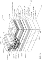
- Fig. 1A schematically shows a perspective view of a normally OFF, GaN FET transistor 20 comprising a drain “DRN", a source “SRC” and, optionally three gates, G1, G2 and G3 located between the source and drain, formed on a heterostructure stack 120 of epitaxially grown semiconductor layers, in accordance with an embodiment of the invention.
- the semiconductor layers have 2DEG current paths for conducting current between source SRC and drain DRN.
- Application of appropriate voltages to the gates controls the current paths to be conducting and non-conducting and the FET correspondingly ON and OFF.
- Fig. 1A it is assumed that no voltages are applied to the gates and the FET is OFF.
- Stack 120 comprises a bottom, optionally high resistance substrate layer 100 on which overlaying layers are epitaxially formed, optionally by a metal organic chemical vapor deposition (MOCVD) growth process.
- MOCVD metal organic chemical vapor deposition
- the layers are grown by a molecular beam epitaxy (MBE) growth process.
- substrate 100 may comprise a single crystal Si, Al 2 O 3 (Sapphire), A1N, or a single crystal polytype of SiC (silicon carbide, carborundum) such as 4H-SiC, 6H-SiC, or 3C-SiC.
- a high resistance Al M Ga 1-M N layer buffer layer 101 is grown on the substrate.
- Buffer layer 101 operates to reduce occurrence of threading and other dislocations in upper layers of stack 120, which may be generated by lattice mismatch between substrate 100 and the upper layers.
- Layer 101 is optionally doped with Fe, W, V, Cr, Ni or Mg to decrease concentration of conduction band electrons in the layer material and enhance the layer's resistance to leakage currents in the transistor that may flow through the layer.
- Layer 101 has a thickness between about 0.5 and about 5 ⁇ m (microns) and M between 0.0 and about 0.05.
- a GaN layer 102 having embedded therein a GaN/AlGaN superlattice 103 is formed over layer 101.
- GaN layer 102 has thickness between about 200 nm and about 400 nm.
- GaN layer 102 has thickness equal to about 300 nm.
- Superlattice 103 comprises a plurality of GaN layers 103a interleaved with Al L Ga 1-L N layers 103b.
- superlattice 103 comprises at least 10 alternating GaN/Al L Ga 1-L N layers 103a/103b.
- Each layer 103a or 103b in the superlattice has thickness between about 1 nm and about 30 nm.
- Interfaces, that is heterojunctions, 103h between the superlattice layers 103a and 103b operate as "mechanical" barriers that moderate propagation of dislocations from layers 100 and 101 into epitaxial layers in stack 120 above layer 102.
- Layer 102 comprising superlattice 103 in accordance with an embodiment of the invention may be considered an additional buffer layer that reduces defect concentrations in active layers located above layer 102, which are controlled to carry current between source SRC and drain DRN.
- Layers 102 and 103 are optionally doped with Fe, W V, Cr, Ni or Mg to increase resistance of the layers to current flow.
- An active layer set 122 of epitaxial layers comprising a normally OFF, non-conducting, 2DEG current channel is grown on layer 102.
- active layer set 122 comprises a relatively narrow band, GaN channel layer 105 contiguous with a relatively wide band In y Al z Ga 1-y-z N electron supply layer 106.
- the 2DEG current channel is located in GaN layer 105 close to an interface, that is, a heterojunction 105h between the GaN and In y Al z Ga 1-y-z N layers 105 and 106.
- the electrostatic fields in layers 105 and 106 are schematically represented by block arrows labeled E 105 and E 106 respectively.
- the 2DEG would make the current channel in GaN layer 105 conducting and able to support current flow between source SRC and drain DRN when no voltages are applied to gates G1, G2 and G3, and result in FET 20 being normally ON.
- active layer set 122 comprises a potential modifying layer 108, having an electrostatic field represented by a block arrow E 108 generated by spontaneous and/or piezoelectric polarization of the layer that has a direction opposite to the electrostatic field E 106 in electron supply layer 106.
- layer 108 comprises In x Ga 1-x N.
- Electric field E 108 generates a potential that operates to reduce a depth of a triangular potential well that might be generated at heterojunction 105h and reduce a number of electrons that might accumulate in the well to create a 2DEG at the heterojunction.
- Potential modifying layer 108 therefore results in the current channel in GaN layer 105 being normally depopulated of electrons and non-conducting, and FET 20 therefore normally OFF.
- active layer set 122 comprises an In x Ga 1-x N layer 104 formed on layer 103 that functions as a barrier layer to improve confinement of electrons to layer 105 when, as discussed below with reference to Figs. 2A and 2B , FET 20 is controlled to be ON and current flows in layer 105.
- Concentration "x" in layer 104 has a value between about 0.05 and about 0.1 and the layer has thickness between about 1 nm and about 2 nm.
- active layer set 122 comprises a GaN transition layer 107 located between layers 106 and 108. Layer 107 operates to enhance lattice matching between layer 106 and layer 108 and layers above layer 108.
- GaN channel layer 105 has thickness between about 5 nm and about 20 nm.
- In y Al z Ga 1-y-z N electron supply layer 106 has thickness between about 8 nm and about 12 nm and has a graded Al mole fraction, which decreases from a about 0.35 at heterojunction 105h with layer 105 to about 0.05 at a heterojunction 106h between layers 106 and 107.
- y is equal to about 0.176 and z is equal to about 4.66y.
- In x Ga 1-x N potential modifying layer 108 has thickness between about 3 nm and 20 nm and x has a value between about 0.08 and about 0.22.
- a second GaN channel layer 109 and associated In y Al z Ga 1-y-z N electron supply layer 111 separated by an AlN spacer layer 110 are formed on layer 108.
- AlN spacer 110 functions to reduce alloy scattering of electrons at a heterojunction 109h and increase electron mobility and density in 2DEGs formed near regions 109G2 and 109G3 of the heterojunction. The 2DEGs are discussed below.
- Layer 109 has thickness between about 1 nm and about 27 nm.
- Layer 111 has thickness between about 8 nm and about 13 nm before formation of recess 130 discussed below.
- AlN spacer layer has thickness between about 0.5 nm and about 3 nm.
- y is equal to about 0.176 and z is equal to about 4.66y.
- a GaN cap layer 112 having thickness between about 0.5 nm and about 4 nm protects surface regions of layer 111 under and in vicinities of drain DRN and source SRC from being oxidized.
- Source and drain terminals SRC and DRN located on cap layer 112 comprise ohmic contact metal stack deposits that are subjected to an annealing process so that metal in the terminals diffuses into underlying active semiconductor layers to promote formation of an ohmic contact between each terminal and the semiconductor layers.
- Metal deposits for conventional ohmic contact terminals are typically formed so that they contact vertical edges of active layers in a mesa of a semiconductor device to which ohmic contact is desired and contact a buffer layer on which the upper epitaxial layers of the mesa is grown.
- diffusion of the metal in the conventional deposits tends to form sharp tipped metallic, "stalactites" that penetrate the buffer layer. Penetration of the stalactites into the buffer layer, and strong electrostatic fields generated by their sharp tips promote leakage currents and tend to damage the buffer and other layers in the mesa.
- metallic deposits for source SRC and drain DRN are deposited only on top, GaN cap layer 112 of FET 20 and are prevented from contact with vertical edges of stack 120.
- Fig. 1B schematically shows formation of stalactites 200 resulting from a conventional production process of ohmic contact terminals 202 for a mesa 204 of semiconductor layers grown on a buffer layer 206.
- the stalactites penetrate the buffer layer and generate intense electric fields at their relatively sharp tips and edges, which fields tend to promote leakage currents in the buffer layer and in an underlying substrate layer 208.
- a leakage current path between sharp points (circled for ease of reference) of the stalactites is schematically indicated by a dashed arrow head line 210.
- Fig. 1C schematically shows formation of stalactites 220 in a production process of an ohmic contact terminal 222 for the same mesa 204 of semiconductor layers shown in Fig. 1B , in accordance with an embodiment of the invention. Because metal for terminals 222 is deposited only on a top layer 205 of mesa 204, and not deposited on edges of layers in the mesa or on buffer layer 206, the stalactites do not penetrate the buffer layer.
- FET 20 is formed having a terraced recess 130, shown in Fig. 1A comprising lower and upper terraces 131 and 132 located respectively in In y Al z Ga 1-y-z N layer 111 and GaN layer 109.
- a layer 113 of insulting insulating material such as Si 3 N 4 , AL 2 O 3 , or AlN, covers surfaces of recess 130 and surface regions of layer 111 along edges of the recess.
- Gate G1 is located on insulating layer 113 that covers lower terrace 131 and gate G3 is located on a portion of insulating layer 113 that covers upper terrace 132.
- Gate G2 is located adjacent source SRC on a portion of insulating layer 113 that covers In y Al z Ga 1-y-z N layer 111.
- GaN channel layer 109, AlN spacer layer 110 and In y Al z Ga 1-y-z N electron supply layer 111 are "intact", that is their thickness, has not been altered by recess 130.
- Energy differences between the conduction and valence bands in GaN channel layer 109 and the conduction and valence bands respectively in In y Al z Ga 1-y-z N layer 111, and electrostatic electric fields generated by polarization in the layers produce a triangular potential well in the GaN layer near a heterojunction region 109G2 and populate the potential well with a 2DEG.
- Fig.1A electrons in the 2DEG are schematically represented by filled circles 109eG2, which numeral is also used to refer to the 2DEG.
- 2DEG 109eG2 has an electron concentration equal to or greater than about 10 13 electrons per cm 2 .
- the potential well is schematically shown in energy band diagrams in Fig. 1D discussed below.
- GaN channel layer 109 and AlN spacer layer 110 are intact, but In y Al z Ga 1-y-z N electron supply layer 111 is thinned down under gate G3 to between about 20% to about 70% of its width under gate G2 by formation of recess 130.
- energy differences between conduction and valence bands in layer 109 and conduction and valence bands in layer 111 and electrostatic fields in the layers populate a 2DEG at a region 109G3 heterojunction of heterojunction 109h between layers 109 and 110. Electrons in the 2DEG, and the 2DEG, are schematically represented by filled circles 109eG3.
- 2DEG 109eG3 under G3 has a smaller accumulation of electrons than 2DEG 109eG2 under gate G2.
- a number of electrons 109eG3 shown in layer 109 under gate G3 is smaller than a number of electrons 109eG2 shown in layer 109 under gate G2.
- 2DEG 109eG3 has an electron concentration equal to or greater than about 3x10 12 electrons per cm 2 .
- Recess 130 has resulted in complete removal of electron supply layer 111 and spacer layer 110 under gate G1. Therefore, in the absence of voltage on gate G1, a 2DEG does not exist under gate G1, and as a result no continuous conductive path capable of carrying current between source SRC and drain DRN exists in layer 109. Nor does a 2DEG exist under gate G1 in any layers of active layer set 122 and therefore the active layer set does not provide a continuous conductive current path between source SRC and drain DRN in the absence of voltage on gate G1.
- active layer set 122 is absent any 2DEGs because of the functioning, in accordance with an embodiment of the invention, of potential modifying layer 108, in preventing generation of a 2DEG in GaN channel layer 105.
- Potential wells (schematically shown in Fig. 1D ) capable of accumulating 2DEG electrons exist in layer 108 along heterojunction regions 108G1, 108G2 and 108G3 between layers 108 and 109, under gates G1, G2 and G3 respectively.
- Potential wells under gates G2 and G3 are populated with electrons 108eG2 under gate G2 and electrons 108eG3 under gate G3.
- the potential well in the current band edge under gate G1, as shown in Fig. 1D has energy substantially greater than the Fermi energy and therefore is substantially without electrons.
- Layer 108 therefore does not provide a conducting current path between source SRC and drain DRN in the absence of voltage applied to gate G1.
- Fig. 1D shows a schematic cross section of FET 20 and graphs 410, 420 and 430 that show energy band diagrams associated with regions of the FET under gates G1, G2 and G3 respectively.
- Dashed lines 411, 421 and 431 indicate regions of FET under gates G1, G2, and G3 characterized by the band diagrams in graphs 410, 420 and 430 respectively.
- Regions in the graphs corresponding to semiconductor layers shown in Fig. 1A are labeled with the same numerals with which they are labeled in Fig. 1A .
- Vertical dashed lines in the graphs indicate heterojunctions between the layers. Regions of the heterojunctions in the graphs associated with regions of heterojunctions in Fig.
- FIG. 1A are indicated by dashed circles labeled with the numerals with which the regions of the heterojunctions are labeled in Fig. 1A .
- Potential energy is shown along an ordinate of each graph and a line E F indicates the Fermi energy level for each band diagram.
- Lines E C and E V in a graph delineate conduction and valence band edges respectively for the region of FET 20 associated with the graph.
- the energy bands shown in graphs 410, 420 and 430 are determined for thickness of layers 102, 103, ... to 108 equal respectively to 1800 nm, 150 nm, 1 nm, 10 nm, 10 nm, 2.6 nm, and 10 nm respectively.
- Under gates G2 and G3 layer 109 is assumed to have thickness of 25 nm and under gate G1 thickness of 5 nm.
- Under gate G2, layers 110, 111 and 112 are assumed to have thickness of 1 nm, 10.7 nm and 1.5 nm respectively.
- Under gate G3 layers 110 and 111 have thickness of 1 nm and 5 nm respectively.
- Dielectric layer 113 has thickness equal to 20 nm.
- electron potential wells exist in regions of heterojunctions between layers 108 and 109 and between layers 109 and 110 indicated respectively by dashed circles 108G2 and 109G2 in the graph, and portions of the potential wells are located below the Fermi energy E F .
- electron potential wells under gate G3 exist in regions of heterojunctions between layers 108 and 109 and between layers 109 and 110 indicated by dashed circles 108G3 and 109G3 respectively in graph 430, and portions of these potential wells are located below the Fermi level E F .
- the potential wells in the regions indicated by the dashed circles are at least partially filled with 2DEG electrons.
- the 2DEGs under gates G2, and electrons in the potential wells that populate the 2DEGs are, as noted above in the discussion of Fig. 1A , schematically represented respectively by filled circles 109eG2 and 108eG2.
- the 2DEGs under gates G3, and electrons in the potential wells that populate the 2DEGs are, as noted above in the discussion of Fig. 1A , schematically represented respectively by filled circles 109eG2 and 108eG2.
- the regions under gates G2 and G3 are, as noted above, referred to as access regions and the 2DEGs 109eG2, 109eG2, 108eG3, and 108eG3 in the access regions provide sources of electrons for rapidly filling electron channels under gate G1 and establishing continuous, low resistance conduction current paths between source SRC and drain DRN when FET 20 is turned ON.
- Voltages applied to gates G1, G2, and G3 operate to generate electric fields in FET 20 that change current paths in the FET between source SRC and drain DRN from substantially non-conducting, high resistance current paths, to conducting, low resistance current paths and turn the FET ON, in accordance with an embodiment of the invention.
- the plurality of gates allows voltages applied to the gates to be configured to shape fields and electrostatic potential in the FET that provide advantageous characteristics for operation of the FET. For example, voltages applied to the gates may be used to moderate potentially damaging large voltage and/or current transients in the FET during transition between ON and OFF states.
- FET 20 comprises three gates
- practice of the invention is not limited to three gates.
- a FET transistor may have four or more gates located between a source and a drain to generate a desired shape electrostatic potential in the FET.
- voltage applied to a gate closer to source SRC to turn FET 20 ON is larger than voltage applied to a gate farther from the source.
- the decreasing voltage regime moderates large swings in voltage and/or current during transition periods between ON and OFF states of FET 20.
- V1, V2, and V3 voltages applied to gates G1, G2, and G3 to turn FET 20 ON are represented by V1, V2, and V3 respectively, then the voltages may have a relationship V2 > V1 > V3.
- V1 and V2 applied to gates G1 and G2 to turn ON the FET are positive.
- V1 is greater than or equal to about 2.0 volts.
- V1 is greater than or equal to about 2.5 volts.
- V2 is greater than or equal to about 2.5 volts.
- V2 is greater than or equal to about 3 volts.
- V3 is less than or equal to about 0 volts.
- V3 is less than or equal to about -1 volt.
- Fig. 2A schematically shows a perspective view of FET 20 when the FET is turned ON by voltages V1, V2, and V3.
- Fig. 2B schematically shows a cross section view of FET 20 in the ON state shown in Fig. 2A .
- Fig. 2B also shows graphs 520, 530 of energy bands E C and E V for access regions of FET 20 under gates G2 and G3 respectively, and a graph 510 of energy bands E C and E V for a region of the FET under gate G1.
- Regions of heterojunctions distinguished by labeled dashed circles in the graphs shown in Fig. 1D are distinguished by dashed circles respectively labeled by the same numerals in the graphs of Fig. 2B .
- the energy bands in graphs 510, 520 and 530 are determined for thickness of layers which are the same as those used to determine the energy band shown in graphs 410, 420, and 430, and V1, V2, and V3, equal respectively to about 2.5 volts, 3 volts, and -1 volt.
- V1 applied to gate G1 reconfigures the conduction band edge E C under the gate shown in graph 410 in Fig. 1D to create potential wells in channel layers 109 and 105 in regions 105G1 and 109G1 of heterojunctions between layers 105 and 106 and between layers 109 and 110 shown in graph 510 of Fig. 2B .
- V1 also lowers conduction band E C so that the newly created potential wells in regions 109G1 and 105G1 and the potential well shown in graph 410 in Fig. 1D in region 108G1 are at least partially below the Fermi energy E F .
- the wells are therefore at least partially filled with electrons that populate 2DEGs in layers 105, 108 and 109 respectively.
- the 2DEGs and the electrons that fill them are represented by filled circles 105eG1, 108eG1 and 109eG1 n Fig. 2A and in the cross section of FET 20 shown in Fig. 2B .
- Voltage V2 applied to gate G2 lowers conduction band E C relative to its position in the OFF state of FET 20 shown in graph 420 of Fig. 1D so that as shown in graph 520 of Fig. 2B , potential wells in regions 109G2 and 108G2 of heterojunction between layer 109 and 110 and between layers 108 and 109 respectively are below the Fermi level. Voltage V2 also creates, or enhances, a potential well in region 105G2 under gate G2, which as shown in graph 520 of Fig. 2B is also below the Fermi level.
- the potential wells in layers 105, 108 and 109 are filled with 2DEGs, schematically represented by filled circles 105eG2, 108eG2 and 109eG2 respectively, in FET 20 shown in Fig. 2A and in the cross section of the FET in Fig. 2B .
- Negative voltage V3 operates to moderate fields and potential drops in the access region under gate G3 and prevent punch through to the drain.
- a plurality of parallel 2DEG conducting current paths is provided between source SRC and drain DRN.
- the parallel current paths shown as shaded regions 500 in layers 105, 106 and 109, "combine” to provide an enhanced 2DEG current path between the source and the drain characterized by a resistance lower than that of any of the component current paths.
- the combined current paths enable FET 20, when ON, to support a relatively large current between source SRC and drain DRN for a relatively small voltage drop between the source and drain and therefore a relatively moderate heat load.
- FET 20 is characterized by an ON resistance between source SRC and drain DRN that is less than or equal to about 75 milliohms for a source SRC to drain DRN current of about 100 amps and voltage between the source and drain equal to about 1700 volts.
- the ON resistance is less than or equal to about 50 milliohms.
- Relatively large quantities of hot electrons are generated in current channels between the source and drain of a FET when it is ON and conducting relatively large currents.
- a portion of the hot electrons propagate towards the FET drain and become trapped in surface states at an interface between a semiconductor channel layer carrying the current and a dielectric layer, such as dielectric layer 113 in FET 20, under the gate and drain access area and/or in traps in the dielectric layer and/or in a passivation layer, such as layer 112, under the drain.
- the trapped electrons generally damage the FET and degrade its operating parameters.
- a FET such as a FET similar to FET 20, in accordance with an embodiment of the invention may have a dielectric layer under its gates charged negatively optionally by embedding electrons in the layer plasma by enhanced chemical vapor deposition or atomic layer deposition.
- the negatively charge dielectric provides a repulsive electric field that operates as a barrier to hot electrons and reduces a probability of hot electrons being trapped at sensitive heterojunction surfaces.
- Fig. 3 schematically shows a portion of a FET 620 similar to FET 20 but having a dielectric layer 613 charged with electrons 614 that operate as a barrier to hot electrons, in accordance with an embodiment of the invention.
- a plurality of FETs are monolithically formed on a suitable substrate in a checkerboard array with each source, SRC of a FET adjacent at least two drains DRNs of other FETs in the array.
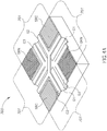
- Fig. 4A schematically shows a monolithically formed array 700 of FETs 701 for which the FETS are fabricated so that their sources SRC and drains DRNs form a checker board pattern.
- FETs 701 are similar to FET 20 and each FET 701 comprises three gates G1, G2 and G3.
- Gates G1 for all the FETs, as shown in Fig. 4A are electrically connected.
- all gates G2 are electrically connected and all gates G3 are electrically connected. Electrical connections between the gates are optionally made at different levels in array 700 as schematically shown in Fig. 4A .
- the gates By growing FETs 701 in a checkerboard array, the gates have relatively large "active" perimeters for controlling 2DEG current channels between sources and drains compared to gates in a conventional array of FETs for which sources are adjacent each other, and a line of adjacent sources is opposite a line of adjacent drains.
- a checkerboard array of FETs in accordance with an embodiment of the invention doubles the active perimeter of the gates in an array compared to a conventional array comprising the same number of FETs. Since ON resistance of a FET and an array of FETs is substantially proportional to active lengths of the gate perimeters, an array of FETs in accordance with an embodiment of the invention may have an ON resistance that is about half that of a conventional array.
- the reduced ON resistance of a checkerboard array in accordance with an embodiment of the invention results in a substantially reduced heat load for the array compared to a conventional array.
- the checkerboard configuration also tends to moderate hot spots in the FET and foster a temperature distribution in the FET that is more uniform than temperature distributions in conventional arrays.
- a checkerboard array in accordance with an embodiment of the invention, is of course not limited to an array having two sources and two drains.
- Fig. 4B schematically shows a checkerboard array 720 of FETs optionally similar to FET 20 ( Fig. 1A ) larger than array 700, in accordance with an embodiment of the invention.
- array 720 has a rectangular shape and comprises two rows 721 and four columns 722 of "interleaved" sources SRC and drains DRN
- an array may have any number of rows and columns.
- a checkerboard array of FETs in accordance with an embodiment of the invention may have a square shape and comprise a same number of rows and columns.
- a checkerboard FET array comprises 36 rows and 36 columns of FETs similar to FET 20 ( Fig. 1A ) and may support 50A of current.
- Fig. 4C shows a schematic cross section in a plane indicated by line AA of checkerboard array 720 shown in Fig. 4B that illustrates providing ohmic contacts to sources SRC and drains DRN of the array, in accordance with an embodiment of the invention.
- Ohmic contacts to sources SRC are optionally provided by a layer of metal 740 deposited over a layer of insulating material such as Si 3 N 4 , AL 2 O 3 , or A1N deposited to cover sources SRC, drains DRN and gates G1, G2, and G3.
- Metal layer 740 is also referred to as source pad 740. Electrical contacts between metal layer 740 and the various sources SRC are made by portions of metal layer 740 deposited in vias 733.
- An insulating layer 734 electrically isolates conducting layer 740 from a layer of metal 742, which provides ohmic contacts to drains DRN. Electrical contacts between metal layer 742 and the various sources SRC are made by portions of metal layer 740 that are deposited in vias 735. Metal in vias 735 are isolated from metal layer 74 by regions of insulating layer 734 and 732. Metal layer 742 is also referred to as drain pad 742.
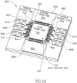
- Fig. 4D schematically shows a FET checkerboard chip 750 comprising an optionally square checkerboard array of FETs mounted and electrically connected to a chip carrier 800 that provides electrical contacts for connecting chip 750 to a PCB, in accordance with an embodiment of the invention.
- Chip drain pad 742 that electrically connects, optionally as shown in Fig. 4C , drains DRN of FET checkerboard chip 750 may be connected to two carrier drain pads 802 comprised in chip carrier 800.
- Carrier drain pads 802 optionally lie along opposite edges of chip 750, and each carrier drain pad 802 is connected to chip drain pad 742 by a plurality of equally spaced, optionally A1, wire bonds 820 that are ball bonded to the chip and carrier drain pads.
- Chip source pad 741 ( Fig. 4C ) that connects all sources SRC in FET checkerboard chip 750 is connected, optionally, by ball bonded A1 wire bonds 822 to carrier source pads 804 located adjacent opposite edges of chip 750, which are perpendicular to the edges of the chip adjacent carrier drain pads 802. Gates G1, G2 and G3 of are electrically connected by wire bonds 824 to carrier gate pads 806, 808 and 810 respectively that are adjacent the same edges of chip 750 that are adjacent carrier source pads 804.
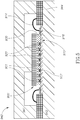
- Fig. 5 schematically shows a cross section of a checkerboard FET chip 900 housed in a heat sink housing 940 comprising top and bottom heat sinks 941 and 942, in accordance with an embodiment of the invention.
- Chip 900 is mounted and electrically connected to a ceramic interconnection substrate 910 that provides electrical contacts for electrically connecting chip 900 to a PCB (not shown). Connection between the chip and interconnection substrate is provided by a ball grid array of solder balls 920 optionally comprising a high temperature solder alloy such as AuSn. The solder balls are optionally formed on contact pads 901 in chip 900 that are electrically connected to gates G1, G2 and G3, and sources SRC and drains DRN ( Figs. 4A, 4B ) of the chip. The solder balls are soldered to corresponding homologous contact pads 912 comprised in interconnection substrate 910 to electrically connect the chip to the interconnect substrate.
- solder balls are soldered to corresponding homologous contact pads 912 comprised in interconnection substrate 910 to electrically connect the chip to the interconnect substrate.
- solder balls are first formed on contact pads 912 in substrate 910 and subsequently soldered to pads 901 in chip 900 to electrically connect the chip and the interconnect substrate.
- Fig. 5 only contact pads 901 connected to sources SRC and drains DRN in chip 900 are shown. Lacunae between chip 900 and substrate 910 are optionally filled with a dielectric adhesive 930 that provides added mechanical stability to contact between the chip and substrate and improves electrical insulation between the solder balls.
- Chip 900 and substrate 910 are sandwiched between upper and lower heat sinks 941 and 942 so that the heat sinks are in good thermal contact with the chip and the substrate.
- Electrical contact to ceramic interconnect substrate 910 from outside heat sink housing 940 is optionally provided by suitable connectors 944 that are wire bonded by wire bonds 914 to "peripheral" contact pads 916 comprised in the interconnect substrate.
- each of the verbs, "comprise” “include” and “have”, and conjugates thereof, are used to indicate that the object or objects of the verb are not necessarily a complete listing of components, elements or parts of the subject or subjects of the verb.
Landscapes
- Junction Field-Effect Transistors (AREA)
Description
- Embodiments of the invention relate to field effect transistors.
- Various products and systems, including consumer products such as TVs, electric powered vehicles, radar systems, electric motor controllers and uninterrupted power supply (UPS) systems, require provision of relatively large amounts of electric power often provided from a high voltage power supply. Various types of semiconductor field effect transistors (FETs) based on silicon materials and technology are generally used as power switches to perform switching functions required by the products and systems.
- A FET typically comprises terminals referred to as a "source" and a "drain" for connecting a power source to a load and a terminal in the FET located between the source and drain referred to as a "gate" for controlling resistance of a current carrying channel in the FET located under the gate between the source and drain. Voltage relative to a common ground voltage applied to the gate generates an electric field in the FET that controls the resistance of the channel to turn the transistor ON and OFF. When turned ON, voltage applied the gate reduces the resistance of the channel to allow relatively large current flow between the source and drain. Total resistance between the source and drain when the transistor is turned ON is referred to as an "ON resistance" of the transistor. The ON resistance depends upon the resistance of the channel, resistance to current flow of a region of the FET under, and in the neighborhood, of the source, and resistance of a region of the FET under, and in the neighborhood, of the drain. The regions under and in the neighborhoods of the source and drain are conventionally referred to as access regions.
- Whereas conventional power FETs based on Si provide useful switching functions, they are not readily configured to provide desired characteristics for power switching applications for, by way of example, operation of devices such as, electric motors and vehicles, uninterruptable power supplies (UPS) and photovoltaic inverters. Switches suitable for operation of these devices are advantageously characterized by relatively high breakdown voltage when they are OFF, high "ON currents" between source and drain when they are ON, and relatively low gate and drain leakage currents. It is advantageous that they are capable of operating at high junction temperatures and that they exhibit good tolerance to current and/or voltage transients that tend to occur during switching between OFF and ON states. In addition, for safety reasons, preferably the switches are OFF when their gates are at ground potential.
- For example, it can be advantageous for a semiconductor power switch to have a breakdown voltage equal to or greater than about 600 V and drain leakage currents less than about 100µA per mm (millimeter) of gate periphery when OFF. When ON it is advantageous that the switch, have an ON resistance less than or about equal to 10 Ohm per mm and be capable of safely supporting a drain current greater than or equal to about 50 A (amps). In addition, for safety reasons, it is generally advantageous that the switch be OFF for gate voltages less than about 2 volts, and be able to operate without damage to itself at junction temperatures greater than or equal to about 200° C. Semiconductor switches based on Si materials and technology are generally not readily configurable to provide these specifications because their band gaps, which are typically less than about 2 eV (electron volts), and saturation drift velocities of electrons in the materials do not naturally support high breakdown voltages and large ON current.
- Nitride based semiconductor materials, such as GaN (Gallium Nitride) and A1N (Aluminum Nitiride) on the other hand, are characterized by relatively large band gaps of 3.4 eV and 6.2 eV respectively. And FETs having a nitride semiconductor layer structure comprising a small band gap layer adjacent a large band gap layer provide a relatively high concentration of high mobility electrons characterized by a high saturation drift velocity. The high mobility electrons accumulate in a narrow triangular potential well at an interface between the layers to form a relatively thin, sheet-like electron concentration, referred to as two dimensional electron gas (2DEG). Because of the geometrical construction and location of the 2DEG, electrons in the 2DEG generally evidence very low donor impurity scattering, and as a result, the relatively high electron mobility, which may for example be equal to about 1.5 x 107 cm/s. Concentrations of electrons in a 2DEG may be as high as 1 x 10¹³/cm2.
- FET transistors that operate by generating and controlling high mobility electrons in 2DEGs are conventionally referred to as high electron mobility transistors "HEMTs". Semiconductor layer structures comprising layers of different composition that characterize these transistors are referred to as "heterostructures", and interfaces between two adjacent layers of different composition are referred to as "heterojunctions".
- Whereas the inherent characteristics of nitride based semiconductor materials appear to make them excellent materials for use in producing high power semiconductor switches, it has proven difficult to exploit the characteristics to provide such switches. For example, 2DEG nitride FETs are normally ON, rather than being the desired, normally OFF, and it has been found difficult to produce nitride semiconductor layers having defect concentrations sufficiently low to produce power FETs having desired characteristics at acceptable costs.
-
US 2009/0146185 A1 discloses a GaN based normally off HEMT with recessed insulated gate. - An embodiment of the invention relates to providing a FET comprising a plurality of nitride semiconductor layers for which piezoelectric and spontaneous polarization of the layers are configured so that the FET is normally OFF and has a relatively large breakdown voltage, and when ON, has relatively small resistance to current flow between a source and drain of the transistor.
- In the invention, the layers in the FET comprise a 2DEG current channel located in a relatively narrow band gap nitride "channel" layer, in a neighborhood of a heterojunction between the channel layer and a relatively wide band gap nitride layer. The wide band gap layer functions as an "electron supply", layer, which provides electrons to the channel layer. The channel and electron supply layers are associated with a third nitride layer, referred to as a "potential modifying layer". In an embodiment of the invention, an electric field generated by piezoelectric and/or spontaneous polarization of the potential modifying layer has a direction opposite to that in the electron supply layer. The electric field of the potential modifying layer modifies an electrostatic potential generated by electrostatic fields resulting from polarization of the channel and electron supply layers to substantially depopulate the 2DEG channel in the first current channel of electrons so that the FET is normally OFF.
- In an embodiment of the invention, the channel and electron supply layers associated with the first 2DEG channel are formed from GaN and InyAlzGa1-y-zN respectively. The potential modifying layer is formed optionally from InxGa1-xN. To mitigate impurity scattering that reduces electron mobility, optionally, the semiconductor materials in the channel and electron supply layers in the FET are not intentionally doped.
- In accordance with the invention, the FET comprises additional 2DEG current channels at heterojunctions of other nitride layers that have 2DEGs in access regions of the FET. The additional 2DEG channels and electrons in the access regions enable establishment of a relatively small resistance current path between the source and drain when the FET is turned ON.
- A plurality of gates are located between the source and drain, and voltages applied to the gates are used to shape fields in the FET that control currents and electron concentrations in the 2DEG current channels. Optionally, the FET is formed having a recess or recesses that have bottom surfaces at different depths below a top layer of the FET. Different gates of the plurality of gates are located on different bottom surfaces of the recess or recesses.
- In an embodiment of the invention, to turn the FET ON voltages that decrease monotonically with distance of the gates from the source are applied to the gates to generate or enhance electron populations in 2DEGs in the plurality of 2DEG channel layers. Optionally, the voltages are configured to moderate current and/or voltage transients in the FET that may appear and damage the FET during transition of the FET from OFF to ON.
- In an embodiment of the invention, layers in the FET comprising the channel and electron supply layers are epitaxially grown over a superlattice structure of thin semiconductor layers that is epitaxially embedded in a buffer layer and doped with compensation impurities. The superlattice structure operates to moderate propagation of dislocations, pipes and other defects from the substrate into the channel and electron supply layers that would tend to reduce electron concentration and mobility of electrons in the channel layers and enhance leakage currents in the FET. The compensation impurities provide the superlattice with increased resistance to current flow.
- In an embodiment of the invention, conducting material for source and drain electrodes is deposited only on a top semiconductor surface of the FET prior to annealing to provide ohmic contact between the source and drain electrodes and current carrying, "active", channel layers of the FET. By limiting deposits of the conducting material for the electrodes to the top layer, distance between the deposits and semiconductor layers below the active layers is maximized. As a result, during annealing, diffusion of conducting material from the deposits to the layers below the active layers is moderated. Moderating diffusion of conducting material to layers below the active layers operates to reduce leakage currents.
- This Summary is provided to introduce a selection of concepts in a simplified form that are further described below in the Detailed Description. This Summary is not intended to identify key features or essential features of the claimed subject matter, nor is it intended to be used to limit the scope of the claimed subject matter.
- Non-limiting examples of embodiments of the invention are described below with reference to figures attached hereto that are listed following this paragraph. Identical structures, elements or parts that appear in more than one figure are generally labeled with a same numeral in all the figures in which they appear. Dimensions of components and features shown in the figures are chosen for convenience and clarity of presentation and are not necessarily shown to scale.
-
Fig. 1A schematically shows a perspective view of a normally OFF FET, optionally comprising three 2DEG channels and three gates, in an OFF state, in accordance with an embodiment of the invention; -
Fig. 1B schematically shows providing a FET with ohmic contact source and drain electrodes in which diffusion of conducting material penetrates to a buffer layer in the FET; -
Fig. 1C schematically show providing the FET shown inFig. 1B with ohmic contact source and drain electrodes in which diffusion of conducting material is prevented from penetrating to the buffer layer in the FET, in accordance with an embodiment of the invention; -
Fig. 1D shows band diagrams for regions of the FET shown inFig. 1A for the OFF state, in accordance with an embodiment of the invention; -
Fig. 2A schematically shows the FET shown inFig. 1A in an ON state, in accordance with an embodiment of the invention; -
Fig. 2B schematically shows energy band diagrams for the FET in the ON state shown inFig. 2A , in accordance with an embodiment of the invention; -
Fig. 3 schematically shows a FET similar to that shown inFigs. 1A and2A and comprising a negatively charged dielectric layer under gates of the FET, in accordance with an embodiment of the invention; -
Figs. 4A and4B schematically show a monolithic array of FETs similar to that shown inFig. 1A configured in a checkerboard pattern, in accordance with an embodiment of the invention; -
Fig. 4C schematically shows a cross section of a portion of the FET array shown inFig. 4B having sources electrically connected by a metal pad and drains connected by a different metal pad electrically isolated from the source pad, in accordance with an embodiment of the invention; -
Fig. 4D schematically shows a chip comprising a checkerboard array of FET and mounted to a chip carrier, in accordance with an embodiment of the invention; and -
Fig. 5 schematically shows a cross section of an array of FETs housed in a heat dissipating housing in accordance with an embodiment of the invention. - In the following paragraphs of the detailed description, structure of a power FET in accordance with an embodiment of the invention and characteristics of 2DEG concentrations in layers of the FET for OFF states are discussed with reference to
Fig. 1 . Methods for providing a semiconductor device, such as the FET shown inFig. 1A , with electrodes that tend to reduce leakage currents in the device are discussed with reference toFigs. 1B and 1C . Band diagrams for the OFF state of the FET are shown inFig. 1D and are discussed with reference to the figures.Fig. 2A schematically shows the FET shown inFig. 1A when the FET is ON. Band diagrams for the ON state of the FET are shown inFig. 1D and are discussed with reference to the figures. - In the discussion unless otherwise stated, adjectives such as "substantially" and "about" modifying a condition or relationship characteristic of a feature or features of an embodiment of the invention, are understood to mean that the condition or characteristic is defined to within tolerances that are acceptable for operation of the embodiment for an application for which it is intended.
-
Fig. 1A schematically shows a perspective view of a normally OFF,GaN FET transistor 20 comprising a drain "DRN", a source "SRC" and, optionally three gates, G1, G2 and G3 located between the source and drain, formed on aheterostructure stack 120 of epitaxially grown semiconductor layers, in accordance with an embodiment of the invention. The semiconductor layers have 2DEG current paths for conducting current between source SRC and drain DRN. Application of appropriate voltages to the gates controls the current paths to be conducting and non-conducting and the FET correspondingly ON and OFF. InFig. 1A it is assumed that no voltages are applied to the gates and the FET is OFF. -
Stack 120 comprises a bottom, optionally highresistance substrate layer 100 on which overlaying layers are epitaxially formed, optionally by a metal organic chemical vapor deposition (MOCVD) growth process. In some embodiments of the invention the layers are grown by a molecular beam epitaxy (MBE) growth process.Substrate 100 may comprise a single crystal Si, Al2O3 (Sapphire), A1N, or a single crystal polytype of SiC (silicon carbide, carborundum) such as 4H-SiC, 6H-SiC, or 3C-SiC. - A high resistance AlMGa1-MN
layer buffer layer 101 is grown on the substrate.Buffer layer 101 operates to reduce occurrence of threading and other dislocations in upper layers ofstack 120, which may be generated by lattice mismatch betweensubstrate 100 and the upper layers.Layer 101 is optionally doped with Fe, W, V, Cr, Ni or Mg to decrease concentration of conduction band electrons in the layer material and enhance the layer's resistance to leakage currents in the transistor that may flow through the layer.Layer 101 has a thickness between about 0.5 and about 5 µm (microns) and M between 0.0 and about 0.05. - A
GaN layer 102 having embedded therein a GaN/AlGaN superlattice 103 is formed overlayer 101.GaN layer 102 has thickness between about 200 nm and about 400 nm. Optionally,GaN layer 102 has thickness equal to about 300 nm.Superlattice 103 comprises a plurality ofGaN layers 103a interleaved with AlLGa1-LN layers 103b. In an embodiment of the invention,superlattice 103 comprises at least 10 alternating GaN/AlLGa1-LN layers 103a/103b. Eachlayer superlattice layers layers stack 120 abovelayer 102.Layer 102 comprisingsuperlattice 103 in accordance with an embodiment of the invention may be considered an additional buffer layer that reduces defect concentrations in active layers located abovelayer 102, which are controlled to carry current between source SRC and drain DRN.Layers - An active layer set 122 of epitaxial layers comprising a normally OFF, non-conducting, 2DEG current channel is grown on
layer 102. In an embodiment of the invention, active layer set 122 comprises a relatively narrow band,GaN channel layer 105 contiguous with a relatively wide band InyAlzGa1-y-zNelectron supply layer 106. The 2DEG current channel is located inGaN layer 105 close to an interface, that is, aheterojunction 105h between the GaN and InyAlzGa1-y-zN layers 105 and 106. - Discontinuity between conduction and valence bands in
GaN layer 105 and conduction and valence bands respectively in InyAlzGa1-y-zN layer 106, and electrostatic fields generated by piezoelectric and spontaneous polarization in the layers would normally produce a triangular potential well in the GaN layer nearheterojunction 105h and populate the potential well with a 2DEG. The electrostatic fields inlayers GaN layer 105 conducting and able to support current flow between source SRC and drain DRN when no voltages are applied to gates G1, G2 and G3, and result inFET 20 being normally ON. - However, in accordance with an embodiment of the invention, active layer set 122 comprises a potential modifying
layer 108, having an electrostatic field represented by a block arrow E108 generated by spontaneous and/or piezoelectric polarization of the layer that has a direction opposite to the electrostatic field E106 inelectron supply layer 106. Optionally,layer 108 comprises InxGa1-xN. Electric field E108 generates a potential that operates to reduce a depth of a triangular potential well that might be generated atheterojunction 105h and reduce a number of electrons that might accumulate in the well to create a 2DEG at the heterojunction. Potential modifyinglayer 108 therefore results in the current channel inGaN layer 105 being normally depopulated of electrons and non-conducting, andFET 20 therefore normally OFF. - In an embodiment of the invention, active layer set 122 comprises an InxGa1-xN layer 104 formed on
layer 103 that functions as a barrier layer to improve confinement of electrons to layer 105 when, as discussed below with reference toFigs. 2A and2B ,FET 20 is controlled to be ON and current flows inlayer 105. Concentration "x" inlayer 104 has a value between about 0.05 and about 0.1 and the layer has thickness between about 1 nm and about 2 nm. Optionally, active layer set 122 comprises aGaN transition layer 107 located betweenlayers Layer 107 operates to enhance lattice matching betweenlayer 106 andlayer 108 and layers abovelayer 108. - In an embodiment of the invention,
GaN channel layer 105 has thickness between about 5 nm and about 20 nm. Optionally, InyAlzGa1-y-zNelectron supply layer 106 has thickness between about 8 nm and about 12 nm and has a graded Al mole fraction, which decreases from a about 0.35 atheterojunction 105h withlayer 105 to about 0.05 at aheterojunction 106h betweenlayers channel layer 105 andelectron supply layer 106, y is equal to about 0.176 and z is equal to about 4.66y. InxGa1-xNpotential modifying layer 108 has thickness between about 3 nm and 20 nm and x has a value between about 0.08 and about 0.22. - A second
GaN channel layer 109 and associated InyAlzGa1-y-zNelectron supply layer 111 separated by anAlN spacer layer 110 are formed onlayer 108.AlN spacer 110 functions to reduce alloy scattering of electrons at aheterojunction 109h and increase electron mobility and density in 2DEGs formed near regions 109G2 and 109G3 of the heterojunction. The 2DEGs are discussed below.Layer 109 has thickness between about 1 nm and about 27 nm.Layer 111 has thickness between about 8 nm and about 13 nm before formation ofrecess 130 discussed below. AlN spacer layer has thickness between about 0.5 nm and about 3 nm. Optionally, as in the case oflayers GaN channel layer 109 andelectron supply layer 111, y is equal to about 0.176 and z is equal to about 4.66y. AGaN cap layer 112 having thickness between about 0.5 nm and about 4 nm protects surface regions oflayer 111 under and in vicinities of drain DRN and source SRC from being oxidized. - Source and drain terminals SRC and DRN located on
cap layer 112 comprise ohmic contact metal stack deposits that are subjected to an annealing process so that metal in the terminals diffuses into underlying active semiconductor layers to promote formation of an ohmic contact between each terminal and the semiconductor layers. - Metal deposits for conventional ohmic contact terminals are typically formed so that they contact vertical edges of active layers in a mesa of a semiconductor device to which ohmic contact is desired and contact a buffer layer on which the upper epitaxial layers of the mesa is grown. During annealing, diffusion of the metal in the conventional deposits tends to form sharp tipped metallic, "stalactites" that penetrate the buffer layer. Penetration of the stalactites into the buffer layer, and strong electrostatic fields generated by their sharp tips promote leakage currents and tend to damage the buffer and other layers in the mesa.
- In accordance with an embodiment of the invention, to prevent formation of metallic stalactites that penetrate to the buffer layer, metallic deposits for source SRC and drain DRN are deposited only on top,
GaN cap layer 112 ofFET 20 and are prevented from contact with vertical edges ofstack 120. -
Fig. 1B schematically shows formation ofstalactites 200 resulting from a conventional production process ofohmic contact terminals 202 for amesa 204 of semiconductor layers grown on abuffer layer 206. The stalactites penetrate the buffer layer and generate intense electric fields at their relatively sharp tips and edges, which fields tend to promote leakage currents in the buffer layer and in anunderlying substrate layer 208. A leakage current path between sharp points (circled for ease of reference) of the stalactites is schematically indicated by a dashedarrow head line 210. -
Fig. 1C schematically shows formation of stalactites 220 in a production process of anohmic contact terminal 222 for thesame mesa 204 of semiconductor layers shown inFig. 1B , in accordance with an embodiment of the invention. Because metal forterminals 222 is deposited only on a top layer 205 ofmesa 204, and not deposited on edges of layers in the mesa or onbuffer layer 206, the stalactites do not penetrate the buffer layer. - In an embodiment of the invention,
FET 20 is formed having aterraced recess 130, shown inFig. 1A comprising lower andupper terraces GaN layer 109. Alayer 113 of insulting insulating material, such as Si3N4, AL2O3, or AlN, covers surfaces ofrecess 130 and surface regions oflayer 111 along edges of the recess. Gate G1 is located on insulatinglayer 113 that coverslower terrace 131 and gate G3 is located on a portion of insulatinglayer 113 that coversupper terrace 132. Gate G2 is located adjacent source SRC on a portion of insulatinglayer 113 that covers InyAlzGa1-y-zN layer 111. - In a region of
FET 20 under gate G2,GaN channel layer 109,AlN spacer layer 110 and InyAlzGa1-y-zNelectron supply layer 111 are "intact", that is their thickness, has not been altered byrecess 130. Energy differences between the conduction and valence bands inGaN channel layer 109 and the conduction and valence bands respectively in InyAlzGa1-y-zN layer 111, and electrostatic electric fields generated by polarization in the layers produce a triangular potential well in the GaN layer near a heterojunction region 109G2 and populate the potential well with a 2DEG. InFig.1A electrons in the 2DEG are schematically represented by filled circles 109eG2, which numeral is also used to refer to the 2DEG. In an embodiment of the invention 2DEG 109eG2 has an electron concentration equal to or greater than about 1013 electrons per cm2. The potential well is schematically shown in energy band diagrams inFig. 1D discussed below. - In a region of
FET 20 under gate G3,GaN channel layer 109 andAlN spacer layer 110 are intact, but InyAlzGa1-y-zNelectron supply layer 111 is thinned down under gate G3 to between about 20% to about 70% of its width under gate G2 by formation ofrecess 130. As in heterojunction region 109G2, energy differences between conduction and valence bands inlayer 109 and conduction and valence bands inlayer 111 and electrostatic fields in the layers populate a 2DEG at a region 109G3 heterojunction ofheterojunction 109h betweenlayers electron supply layer 111 under gate G3 is thinner than the region ofelectron supply layer 111 under G2, 2DEG 109eG3 under G3 has a smaller accumulation of electrons than 2DEG 109eG2 under gate G2. To schematically indicate the relative sizes of the 2DEGs under gates G2 and G3, a number of electrons 109eG3 shown inlayer 109 under gate G3 is smaller than a number of electrons 109eG2 shown inlayer 109 under gate G2. In an embodiment of the invention 2DEG 109eG3 has an electron concentration equal to or greater than about 3x10¹² electrons per cm2. -
Recess 130 has resulted in complete removal ofelectron supply layer 111 andspacer layer 110 under gate G1. Therefore, in the absence of voltage on gate G1, a 2DEG does not exist under gate G1, and as a result no continuous conductive path capable of carrying current between source SRC and drain DRN exists inlayer 109. Nor does a 2DEG exist under gate G1 in any layers of active layer set 122 and therefore the active layer set does not provide a continuous conductive current path between source SRC and drain DRN in the absence of voltage on gate G1. - As discussed above, active layer set 122 is absent any 2DEGs because of the functioning, in accordance with an embodiment of the invention, of potential modifying
layer 108, in preventing generation of a 2DEG inGaN channel layer 105. Potential wells (schematically shown inFig. 1D ) capable of accumulating 2DEG electrons exist inlayer 108 along heterojunction regions 108G1, 108G2 and 108G3 betweenlayers Fig. 1D has energy substantially greater than the Fermi energy and therefore is substantially without electrons.Layer 108 therefore does not provide a conducting current path between source SRC and drain DRN in the absence of voltage applied to gate G1. - As a result, as shown for
FET 20 inFig. 1A , in the absence of appropriate voltages on gate G1, and gates G2 and G3, continuous conduction paths in the FET between source SRC and drain DRN are substantially non-existent, and the FET is OFF. -
Fig. 1D shows a schematic cross section ofFET 20 andgraphs lines graphs Fig. 1A are labeled with the same numerals with which they are labeled inFig. 1A . Vertical dashed lines in the graphs indicate heterojunctions between the layers. Regions of the heterojunctions in the graphs associated with regions of heterojunctions inFig. 1A are indicated by dashed circles labeled with the numerals with which the regions of the heterojunctions are labeled inFig. 1A . Potential energy is shown along an ordinate of each graph and a line EF indicates the Fermi energy level for each band diagram. Lines EC and EV in a graph delineate conduction and valence band edges respectively for the region ofFET 20 associated with the graph. - By way of a numerical example, the energy bands shown in
graphs layers G3 layer 109 is assumed to have thickness of 25 nm and under gate G1 thickness of 5 nm. Under gate G2, layers 110, 111 and 112 are assumed to have thickness of 1 nm, 10.7 nm and 1.5 nm respectively. Under gate G3 layers 110 and 111 have thickness of 1 nm and 5 nm respectively.Dielectric layer 113 has thickness equal to 20 nm. - In
graph 410, which shows conduction and valence band edges EC and EV for the region ofFET 20 under gate G1, conduction band edge EC is displaced above the Fermi energy EF. As a result, the conduction band, and a potential well in a region indicated by a dashed circle 108G1, of the heterojunction betweenlayers layers graph 410, depth of lower terrace 131 (Fig. 1 ), and differences in conduction band and valence band energy levels of layers 105-109 substantially eliminate potential wells capable of accumulating 2DEG electrons. The absence of any concentration of 2DEG electrons under gate G1 rendersFET 20 OFF when no voltages are applied to gate G1. - Under G2, as shown in
graph 420 on the other hand, electron potential wells exist in regions of heterojunctions betweenlayers layers layers layers graph 430, and portions of these potential wells are located below the Fermi level EF. As a result, the potential wells in the regions indicated by the dashed circles are at least partially filled with 2DEG electrons. - The 2DEGs under gates G2, and electrons in the potential wells that populate the 2DEGs are, as noted above in the discussion of
Fig. 1A , schematically represented respectively by filled circles 109eG2 and 108eG2. Similarly, the 2DEGs under gates G3, and electrons in the potential wells that populate the 2DEGs are, as noted above in the discussion ofFig. 1A , schematically represented respectively by filled circles 109eG2 and 108eG2. - The regions under gates G2 and G3 are, as noted above, referred to as access regions and the 2DEGs 109eG2, 109eG2, 108eG3, and 108eG3 in the access regions provide sources of electrons for rapidly filling electron channels under gate G1 and establishing continuous, low resistance conduction current paths between source SRC and drain DRN when
FET 20 is turned ON. - Voltages applied to gates G1, G2, and G3 operate to generate electric fields in
FET 20 that change current paths in the FET between source SRC and drain DRN from substantially non-conducting, high resistance current paths, to conducting, low resistance current paths and turn the FET ON, in accordance with an embodiment of the invention. The plurality of gates allows voltages applied to the gates to be configured to shape fields and electrostatic potential in the FET that provide advantageous characteristics for operation of the FET. For example, voltages applied to the gates may be used to moderate potentially damaging large voltage and/or current transients in the FET during transition between ON and OFF states. - It is noted that whereas
FET 20 comprises three gates, practice of the invention is not limited to three gates. For example, a FET transistor may have four or more gates located between a source and a drain to generate a desired shape electrostatic potential in the FET. - In an embodiment of the invention, voltage applied to a gate closer to source SRC to turn
FET 20 ON is larger than voltage applied to a gate farther from the source. The decreasing voltage regime moderates large swings in voltage and/or current during transition periods between ON and OFF states ofFET 20. In symbols, if voltages applied to gates G1, G2, and G3 to turnFET 20 ON are represented by V1, V2, and V3 respectively, then the voltages may have a relationship V2 > V1 > V3. - For a configuration of a normally OFF FET, such as
FET 20, in accordance with an embodiment of the invention, voltages V1 and V2 applied to gates G1 and G2 to turn ON the FET are positive. In an embodiment of the invention, V1 is greater than or equal to about 2.0 volts. Optionally V1 is greater than or equal to about 2.5 volts. In an embodiment of the invention V2 is greater than or equal to about 2.5 volts. Optionally, V2 is greater than or equal to about 3 volts. In an embodiment of the invention V3 is less than or equal to about 0 volts. Optionally V3 is less than or equal to about -1 volt. -
Fig. 2A schematically shows a perspective view ofFET 20 when the FET is turned ON by voltages V1, V2, and V3.Fig. 2B schematically shows a cross section view ofFET 20 in the ON state shown inFig. 2A .Fig. 2B also showsgraphs FET 20 under gates G2 and G3 respectively, and agraph 510 of energy bands EC and EV for a region of the FET under gate G1. Regions of heterojunctions distinguished by labeled dashed circles in the graphs shown inFig. 1D are distinguished by dashed circles respectively labeled by the same numerals in the graphs ofFig. 2B . - By way of a numerical example, the energy bands in
graphs graphs - Positive voltage V1 applied to gate G1 reconfigures the conduction band edge EC under the gate shown in
graph 410 inFig. 1D to create potential wells inchannel layers layers layers graph 510 ofFig. 2B . V1 also lowers conduction band EC so that the newly created potential wells in regions 109G1 and 105G1 and the potential well shown ingraph 410 inFig. 1D in region 108G1 are at least partially below the Fermi energy EF. The wells are therefore at least partially filled with electrons that populate 2DEGs inlayers Fig. 2A and in the cross section ofFET 20 shown inFig. 2B . - Voltage V2 applied to gate G2 lowers conduction band EC relative to its position in the OFF state of
FET 20 shown ingraph 420 ofFig. 1D so that as shown ingraph 520 ofFig. 2B , potential wells in regions 109G2 and 108G2 of heterojunction betweenlayer layers graph 520 ofFig. 2B is also below the Fermi level. The potential wells inlayers FET 20 shown inFig. 2A and in the cross section of the FET inFig. 2B . Negative voltage V3, operates to moderate fields and potential drops in the access region under gate G3 and prevent punch through to the drain. - As a result of the creation of 2DEGs under gate G1 in
layers layers layer 105, a plurality of parallel 2DEG conducting current paths is provided between source SRC and drain DRN. The parallel current paths, shown as shadedregions 500 inlayers FET 20, when ON, to support a relatively large current between source SRC and drain DRN for a relatively small voltage drop between the source and drain and therefore a relatively moderate heat load. - In an embodiment of the
invention FET 20 is characterized by an ON resistance between source SRC and drain DRN that is less than or equal to about 75 milliohms for a source SRC to drain DRN current of about 100 amps and voltage between the source and drain equal to about 1700 volts. Optionally the ON resistance is less than or equal to about 50 milliohms. - Relatively large quantities of hot electrons are generated in current channels between the source and drain of a FET when it is ON and conducting relatively large currents. A portion of the hot electrons propagate towards the FET drain and become trapped in surface states at an interface between a semiconductor channel layer carrying the current and a dielectric layer, such as
dielectric layer 113 inFET 20, under the gate and drain access area and/or in traps in the dielectric layer and/or in a passivation layer, such aslayer 112, under the drain. The trapped electrons generally damage the FET and degrade its operating parameters. - A FET, such as a FET similar to
FET 20, in accordance with an embodiment of the invention may have a dielectric layer under its gates charged negatively optionally by embedding electrons in the layer plasma by enhanced chemical vapor deposition or atomic layer deposition. The negatively charge dielectric provides a repulsive electric field that operates as a barrier to hot electrons and reduces a probability of hot electrons being trapped at sensitive heterojunction surfaces.Fig. 3 schematically shows a portion of aFET 620 similar toFET 20 but having adielectric layer 613 charged withelectrons 614 that operate as a barrier to hot electrons, in accordance with an embodiment of the invention. - In an embodiment of the invention, a plurality of FETs, optionally similar to
FET 20, are monolithically formed on a suitable substrate in a checkerboard array with each source, SRC of a FET adjacent at least two drains DRNs of other FETs in the array.Fig. 4A schematically shows a monolithically formedarray 700 ofFETs 701 for which the FETS are fabricated so that their sources SRC and drains DRNs form a checker board pattern.Optionally FETs 701 are similar toFET 20 and eachFET 701 comprises three gates G1, G2 and G3. For convenience of presentation, semiconductor layers in the FETs under the drains and gates are not shown. Gates G1 for all the FETs, as shown inFig. 4A , are electrically connected. Similarly, all gates G2 are electrically connected and all gates G3 are electrically connected. Electrical connections between the gates are optionally made at different levels inarray 700 as schematically shown inFig. 4A . - By growing
FETs 701 in a checkerboard array, the gates have relatively large "active" perimeters for controlling 2DEG current channels between sources and drains compared to gates in a conventional array of FETs for which sources are adjacent each other, and a line of adjacent sources is opposite a line of adjacent drains. In general, a checkerboard array of FETs in accordance with an embodiment of the invention doubles the active perimeter of the gates in an array compared to a conventional array comprising the same number of FETs. Since ON resistance of a FET and an array of FETs is substantially proportional to active lengths of the gate perimeters, an array of FETs in accordance with an embodiment of the invention may have an ON resistance that is about half that of a conventional array. For a given current, the reduced ON resistance of a checkerboard array in accordance with an embodiment of the invention results in a substantially reduced heat load for the array compared to a conventional array. The checkerboard configuration also tends to moderate hot spots in the FET and foster a temperature distribution in the FET that is more uniform than temperature distributions in conventional arrays. - A checkerboard array, in accordance with an embodiment of the invention, is of course not limited to an array having two sources and two drains. For example,
Fig. 4B schematically shows acheckerboard array 720 of FETs optionally similar to FET 20 (Fig. 1A ) larger thanarray 700, in accordance with an embodiment of the invention. It is noted that whereasarray 720 has a rectangular shape and comprises tworows 721 and fourcolumns 722 of "interleaved" sources SRC and drains DRN, an array may have any number of rows and columns. For example, a checkerboard array of FETs in accordance with an embodiment of the invention may have a square shape and comprise a same number of rows and columns. In an embodiment of the invention a checkerboard FET array comprises 36 rows and 36 columns of FETs similar to FET 20 (Fig. 1A ) and may support 50A of current. -
Fig. 4C shows a schematic cross section in a plane indicated by line AA ofcheckerboard array 720 shown inFig. 4B that illustrates providing ohmic contacts to sources SRC and drains DRN of the array, in accordance with an embodiment of the invention. Ohmic contacts to sources SRC are optionally provided by a layer ofmetal 740 deposited over a layer of insulating material such as Si3N4, AL2O3, or A1N deposited to cover sources SRC, drains DRN and gates G1, G2, and G3.Metal layer 740 is also referred to assource pad 740. Electrical contacts betweenmetal layer 740 and the various sources SRC are made by portions ofmetal layer 740 deposited invias 733. An insulatinglayer 734 electricallyisolates conducting layer 740 from a layer ofmetal 742, which provides ohmic contacts to drains DRN. Electrical contacts betweenmetal layer 742 and the various sources SRC are made by portions ofmetal layer 740 that are deposited invias 735. Metal invias 735 are isolated from metal layer 74 by regions of insulatinglayer Metal layer 742 is also referred to asdrain pad 742. -
Fig. 4D schematically shows aFET checkerboard chip 750 comprising an optionally square checkerboard array of FETs mounted and electrically connected to achip carrier 800 that provides electrical contacts for connectingchip 750 to a PCB, in accordance with an embodiment of the invention.Chip drain pad 742 that electrically connects, optionally as shown inFig. 4C , drains DRN ofFET checkerboard chip 750 may be connected to twocarrier drain pads 802 comprised inchip carrier 800.Carrier drain pads 802 optionally lie along opposite edges ofchip 750, and eachcarrier drain pad 802 is connected to chipdrain pad 742 by a plurality of equally spaced, optionally A1,wire bonds 820 that are ball bonded to the chip and carrier drain pads. Chip source pad 741 (Fig. 4C ) that connects all sources SRC inFET checkerboard chip 750 is connected, optionally, by ball bondedA1 wire bonds 822 tocarrier source pads 804 located adjacent opposite edges ofchip 750, which are perpendicular to the edges of the chip adjacentcarrier drain pads 802. Gates G1, G2 and G3 of are electrically connected bywire bonds 824 tocarrier gate pads chip 750 that are adjacentcarrier source pads 804. -
Fig. 5 schematically shows a cross section of acheckerboard FET chip 900 housed in aheat sink housing 940 comprising top andbottom heat sinks -
Chip 900 is mounted and electrically connected to aceramic interconnection substrate 910 that provides electrical contacts for electrically connectingchip 900 to a PCB (not shown). Connection between the chip and interconnection substrate is provided by a ball grid array ofsolder balls 920 optionally comprising a high temperature solder alloy such as AuSn. The solder balls are optionally formed oncontact pads 901 inchip 900 that are electrically connected to gates G1, G2 and G3, and sources SRC and drains DRN (Figs. 4A, 4B ) of the chip. The solder balls are soldered to correspondinghomologous contact pads 912 comprised ininterconnection substrate 910 to electrically connect the chip to the interconnect substrate. Optionally, the solder balls are first formed oncontact pads 912 insubstrate 910 and subsequently soldered topads 901 inchip 900 to electrically connect the chip and the interconnect substrate. InFig. 5 only contactpads 901 connected to sources SRC and drains DRN inchip 900 are shown. Lacunae betweenchip 900 andsubstrate 910 are optionally filled with adielectric adhesive 930 that provides added mechanical stability to contact between the chip and substrate and improves electrical insulation between the solder balls. -
Chip 900 andsubstrate 910 are sandwiched between upper andlower heat sinks ceramic interconnect substrate 910 from outsideheat sink housing 940 is optionally provided bysuitable connectors 944 that are wire bonded bywire bonds 914 to "peripheral"contact pads 916 comprised in the interconnect substrate. - In the description and claims of the present application, each of the verbs, "comprise" "include" and "have", and conjugates thereof, are used to indicate that the object or objects of the verb are not necessarily a complete listing of components, elements or parts of the subject or subjects of the verb.
- Descriptions of embodiments of the invention in the present application are provided by way of example and are not intended to limit the scope of the invention. The described embodiments comprise different features, not all of which are required in all embodiments of the invention. Some embodiments utilize only some of the features or possible combinations of the features. Variations of embodiments of the invention that are described, and embodiments of the invention comprising different combinations of features noted in the described embodiments, will occur to persons of the art. The scope of the invention is limited only by the claims.
Claims (13)
- A normally OFF field effect transistor (FET) comprising:a plurality of contiguous nitride semiconductor layers; anda source (SRC) and a drain (DRN) overlying a top nitride layer (112) of the plurality of nitride layers and having source and drain access regions respectively comprising regions of at least two heterojunctions between the nitride layers near the source and drain;a first gate (G1) between the source (SRC) and drain (DRN); anda set of nitride layers comprised in the plurality of nitride layers, the set comprising:a first nitride layer (105) having a first band gap;a second nitride layer (106) that forms a first said heterojunction with the first layer and having a second band gap wider than the first band gap and polarization that generates an electrostatic field (E106) in the second layer having a direction that causes electron drift towards the first heterojunction;a third nitride layer (108) located on a same side of the first nitride layer as the second nitride layer having polarization that generates an electrostatic field (E108) in a direction opposite to the electric field in the second nitride layer which raises the conduction band at the first heterojunction under the first gate above the Fermi energy;a fourth nitride layer (109) formed from GaN having band gap greater than the third layer that forms a second said heterojunction with the third layer having a two dimensional electron gas (2DEG) (108eG2, 108eG3) in the source and drain access regions but not in a region (108G1) below the first gate (G1) in the absence of a voltage applied to the first gate (Gl); anda fifth nitride layer (111) formed from InAlGaN having band gap greater than the fourth nitride layer and polarization that generates an electrostatic field in the fifth nitride layer that causes electron drift towards the fourth layer and wherein the fourth nitride layer forms a third said heterojunction (109G2, 109G3) with the fifth nitride layer or with a nitride layer intermediate the fourth and fifth nitride layers that has a 2DEG (109eG2, 109eG3) in the source and drain access regions;wherein the plurality of layers is formed having a recess (130) which extends into and has a recess surface (131) at the first gate (G1) in the fourth layer (109) that is covered by an insulating layer (113);wherein a positive voltage applied to the first gate lowers the conduction band at the first heterojunction in a region under the first gate, to generate a plurality of parallel 2DEGs (105eG1, 108eG1, 109eG1) which couple the two 2DEGs (108eG2, 108eG3, 109eG2, 109eG3) in each of the access regions with a conducting channel through the plurality of nitride layers to form a continuous electrically conducting path between the source and drain that turns the FET ON.
- A FET according to claim 1 wherein the second layer comprises InyAlzGa1-y-zN.
- A FET according to claim 2 wherein the InyAlzGa1-y-zN layer has thickness between about 8 nm and about 12 nm.
- A FET according to any of claim 1-3 wherein the third layer is above, and thereby closer to the source and drain, than the first and second layers.
- A FET according to claim to any of claims 1-4 wherein the third layer comprises InxGa1-xN.
- A FET according to claim 5 wherein x has a value between about 0.08 and about 0.11.
- A FET according to any of the preceding claims wherein the insulating layer is negatively charged.
- A FET according to any of the preceding claims wherein the fourth layer on either side of the recess has thickness between about 1 nm and about 17 nm.
- A FET according to any of the preceding claims and comprising second and third gates (G2, G3) on opposite sides of the first gate (G1) that respectively overlie access regions of the source (SRC) and drain (DRN) at the fifth nitride layer.
- A FET according to claim 9 wherein the plurality of contiguous nitride layers is formed having a recess that extends into and has a recess surface located in the fifth nitride layer.
- A FET according to claim 10 wherein the third gate is located on an insulating layer covering the recess surface in the fifth nitride layer.
- A FET according to claim 11 wherein the insulating layer is negatively charged.
- A FET according to any of claims 9-12 and comprising a power supply that applies voltages V1, V2, and V3, to the first, second, and third gates (G1, G2, G3) respectively when turning the FET ON, wherein the voltages are related by a relationship V2 > V1 > V3.
Applications Claiming Priority (2)
| Application Number | Priority Date | Filing Date | Title |
|---|---|---|---|
| US33036110P | 2010-05-02 | 2010-05-02 | |
| PCT/IB2011/051939 WO2011138732A1 (en) | 2010-05-02 | 2011-05-02 | Field effect power transistors |
Publications (2)
| Publication Number | Publication Date |
|---|---|
| EP2567404A1 EP2567404A1 (en) | 2013-03-13 |
| EP2567404B1 true EP2567404B1 (en) | 2017-07-12 |
Family
ID=44120334
Family Applications (1)
| Application Number | Title | Priority Date | Filing Date |
|---|---|---|---|
| EP11722569.8A Active EP2567404B1 (en) | 2010-05-02 | 2011-05-02 | Field effect power transistors |
Country Status (5)
| Country | Link |
|---|---|
| EP (1) | EP2567404B1 (en) |
| JP (1) | JP2013526076A (en) |
| KR (1) | KR20130059357A (en) |
| SG (2) | SG2014013809A (en) |
| WO (1) | WO2011138732A1 (en) |
Families Citing this family (3)
| Publication number | Priority date | Publication date | Assignee | Title |
|---|---|---|---|---|
| KR101985503B1 (en) * | 2017-08-18 | 2019-06-04 | 전북대학교 산학협력단 | Nitride semiconductor device |
| IT201900001201A1 (en) * | 2019-01-28 | 2020-07-28 | St Microelectronics Srl | SEMICONDUCTOR PLATE WITH IMPROVED THERMAL INSULATION BETWEEN A POWER PORTION AND A PERIPHERAL PORTION, MANUFACTURING METHOD, AND PACKAGE HOUSING THE PLATE |
| CN113436963B (en) * | 2021-06-28 | 2022-05-20 | 吉林大学 | Covering layer screening method for two-dimensional semiconductor modulation doping and obtained heterojunction |
Family Cites Families (16)
| Publication number | Priority date | Publication date | Assignee | Title |
|---|---|---|---|---|
| JP3441353B2 (en) * | 1998-01-29 | 2003-09-02 | 京セラ株式会社 | Field-effect transistor |
| JP3209270B2 (en) * | 1999-01-29 | 2001-09-17 | 日本電気株式会社 | Heterojunction field effect transistor |
| JP2003151996A (en) * | 2001-09-03 | 2003-05-23 | Nichia Chem Ind Ltd | Electronic device using two-dimensional electron gas |
| US6825559B2 (en) * | 2003-01-02 | 2004-11-30 | Cree, Inc. | Group III nitride based flip-chip intergrated circuit and method for fabricating |
| JP4826703B2 (en) * | 2004-09-29 | 2011-11-30 | サンケン電気株式会社 | Plate-like substrate for use in forming semiconductor elements |
| US8183595B2 (en) * | 2005-07-29 | 2012-05-22 | International Rectifier Corporation | Normally off III-nitride semiconductor device having a programmable gate |
| US7595245B2 (en) * | 2005-08-12 | 2009-09-29 | Texas Instruments Incorporated | Semiconductor device having a gate electrode material feature located adjacent a gate width side of its gate electrode and a method of manufacture therefor |
| JP2007109830A (en) * | 2005-10-12 | 2007-04-26 | Univ Nagoya | Field effect transistor |
| JP4282708B2 (en) * | 2006-10-20 | 2009-06-24 | 株式会社東芝 | Nitride semiconductor devices |
| GB2459422A (en) * | 2007-02-16 | 2009-10-28 | Sumitomo Chemical Co | Epitaxial substrate for field effect transistor |
| US20090072269A1 (en) * | 2007-09-17 | 2009-03-19 | Chang Soo Suh | Gallium nitride diodes and integrated components |
| CN101897029B (en) * | 2007-12-10 | 2015-08-12 | 特兰斯夫公司 | Insulated Gate E-Mode Transistor |
| JP5470705B2 (en) * | 2007-12-28 | 2014-04-16 | サンケン電気株式会社 | Semiconductor device and manufacturing method thereof |
| CN101981658B (en) * | 2008-03-24 | 2014-10-29 | 日本碍子株式会社 | Semiconductor element, epitaxial substrate for semiconductor element, and manufacturing method thereof |
| US7985986B2 (en) * | 2008-07-31 | 2011-07-26 | Cree, Inc. | Normally-off semiconductor devices |
| US8759876B2 (en) * | 2008-10-06 | 2014-06-24 | Massachusetts Institute Of Technology | Enhancement-mode nitride transistor |
-
2011
- 2011-05-02 SG SG2014013809A patent/SG2014013809A/en unknown
- 2011-05-02 KR KR1020127031548A patent/KR20130059357A/en not_active Withdrawn
- 2011-05-02 WO PCT/IB2011/051939 patent/WO2011138732A1/en not_active Ceased
- 2011-05-02 EP EP11722569.8A patent/EP2567404B1/en active Active
- 2011-05-02 SG SG2012080768A patent/SG185120A1/en unknown
- 2011-05-02 JP JP2013508602A patent/JP2013526076A/en active Pending
Also Published As
| Publication number | Publication date |
|---|---|
| EP2567404A1 (en) | 2013-03-13 |
| KR20130059357A (en) | 2013-06-05 |
| WO2011138732A1 (en) | 2011-11-10 |
| SG185120A1 (en) | 2012-11-29 |
| SG2014013809A (en) | 2014-04-28 |
| JP2013526076A (en) | 2013-06-20 |
Similar Documents
| Publication | Publication Date | Title |
|---|---|---|
| EP2748855B1 (en) | Field effect power transistors | |
| CN1957474B (en) | Ⅲ-Nitrogen current control device and its manufacturing method | |
| US7898004B2 (en) | Semiconductor heterostructure diodes | |
| TWI450383B (en) | Semiconductor structure, integrated circuit including semiconductor structure, and method for fabricating semiconductor structure | |
| EP2713402B1 (en) | Normally-off high electron mobility transistor | |
| US20250040175A1 (en) | A vertical hemt, an electrical circuit, and a method for producing a vertical hemt | |
| WO2017210323A1 (en) | Iii-nitride devices including a graded depleting layer | |
| JP7509746B2 (en) | External field termination structures for improving the reliability of high voltage, high power active devices. | |
| TWI775276B (en) | High electron mobility transistor and fabrication method thereof | |
| KR102071019B1 (en) | Nitride high electron mobility transistor and manufacturing method thereof | |
| US20100187569A1 (en) | Hetero-structure field effect transistor, integrated circuit including a hetero-structure field effect transistor and method for manufacturing a hetero-structure field effect transistor | |
| CN104704615B (en) | switching element | |
| US20170330944A1 (en) | Normally-off hetrojunction transistor with high threshold voltage | |
| EP2567404A1 (en) | Field effect power transistors | |
| JP2007180330A (en) | Semiconductor device and its manufacturing method | |
| KR20250128073A (en) | Semiconductor device | |
| KR20250094031A (en) | Semiconductor device | |
| KR20260013701A (en) | Semiconductor device | |
| KR20250087270A (en) | Semiconductor device | |
| KR20140133755A (en) | Nitride high electron mobility transistor and manufacturing method thereof |
Legal Events
| Date | Code | Title | Description |
|---|---|---|---|
| PUAI | Public reference made under article 153(3) epc to a published international application that has entered the european phase |
Free format text: ORIGINAL CODE: 0009012 |
|
| 17P | Request for examination filed |
Effective date: 20121203 |
|
| AK | Designated contracting states |
Kind code of ref document: A1 Designated state(s): AL AT BE BG CH CY CZ DE DK EE ES FI FR GB GR HR HU IE IS IT LI LT LU LV MC MK MT NL NO PL PT RO RS SE SI SK SM TR |
|
| DAX | Request for extension of the european patent (deleted) | ||
| 17Q | First examination report despatched |
Effective date: 20150518 |
|
| GRAP | Despatch of communication of intention to grant a patent |
Free format text: ORIGINAL CODE: EPIDOSNIGR1 |
|
| STAA | Information on the status of an ep patent application or granted ep patent |
Free format text: STATUS: GRANT OF PATENT IS INTENDED |
|
| INTG | Intention to grant announced |
Effective date: 20161110 |
|
| GRAS | Grant fee paid |
Free format text: ORIGINAL CODE: EPIDOSNIGR3 |
|
| GRAA | (expected) grant |
Free format text: ORIGINAL CODE: 0009210 |
|
| STAA | Information on the status of an ep patent application or granted ep patent |
Free format text: STATUS: THE PATENT HAS BEEN GRANTED |
|
| AK | Designated contracting states |
Kind code of ref document: B1 Designated state(s): AL AT BE BG CH CY CZ DE DK EE ES FI FR GB GR HR HU IE IS IT LI LT LU LV MC MK MT NL NO PL PT RO RS SE SI SK SM TR |
|
| REG | Reference to a national code |
Ref country code: GB Ref legal event code: FG4D |
|
| REG | Reference to a national code |
Ref country code: CH Ref legal event code: EP |
|
| REG | Reference to a national code |
Ref country code: AT Ref legal event code: REF Ref document number: 909099 Country of ref document: AT Kind code of ref document: T Effective date: 20170715 |
|
| REG | Reference to a national code |
Ref country code: IE Ref legal event code: FG4D |
|
| REG | Reference to a national code |
Ref country code: DE Ref legal event code: R096 Ref document number: 602011039466 Country of ref document: DE |
|
| REG | Reference to a national code |
Ref country code: NL Ref legal event code: MP Effective date: 20170712 |
|
| REG | Reference to a national code |
Ref country code: LT Ref legal event code: MG4D |
|
| PG25 | Lapsed in a contracting state [announced via postgrant information from national office to epo] |
Ref country code: HR Free format text: LAPSE BECAUSE OF FAILURE TO SUBMIT A TRANSLATION OF THE DESCRIPTION OR TO PAY THE FEE WITHIN THE PRESCRIBED TIME-LIMIT Effective date: 20170712 Ref country code: FI Free format text: LAPSE BECAUSE OF FAILURE TO SUBMIT A TRANSLATION OF THE DESCRIPTION OR TO PAY THE FEE WITHIN THE PRESCRIBED TIME-LIMIT Effective date: 20170712 Ref country code: SE Free format text: LAPSE BECAUSE OF FAILURE TO SUBMIT A TRANSLATION OF THE DESCRIPTION OR TO PAY THE FEE WITHIN THE PRESCRIBED TIME-LIMIT Effective date: 20170712 Ref country code: LT Free format text: LAPSE BECAUSE OF FAILURE TO SUBMIT A TRANSLATION OF THE DESCRIPTION OR TO PAY THE FEE WITHIN THE PRESCRIBED TIME-LIMIT Effective date: 20170712 Ref country code: NO Free format text: LAPSE BECAUSE OF FAILURE TO SUBMIT A TRANSLATION OF THE DESCRIPTION OR TO PAY THE FEE WITHIN THE PRESCRIBED TIME-LIMIT Effective date: 20171012 Ref country code: NL Free format text: LAPSE BECAUSE OF FAILURE TO SUBMIT A TRANSLATION OF THE DESCRIPTION OR TO PAY THE FEE WITHIN THE PRESCRIBED TIME-LIMIT Effective date: 20170712 |
|
| PG25 | Lapsed in a contracting state [announced via postgrant information from national office to epo] |
Ref country code: PL Free format text: LAPSE BECAUSE OF FAILURE TO SUBMIT A TRANSLATION OF THE DESCRIPTION OR TO PAY THE FEE WITHIN THE PRESCRIBED TIME-LIMIT Effective date: 20170712 Ref country code: ES Free format text: LAPSE BECAUSE OF FAILURE TO SUBMIT A TRANSLATION OF THE DESCRIPTION OR TO PAY THE FEE WITHIN THE PRESCRIBED TIME-LIMIT Effective date: 20170712 Ref country code: GR Free format text: LAPSE BECAUSE OF FAILURE TO SUBMIT A TRANSLATION OF THE DESCRIPTION OR TO PAY THE FEE WITHIN THE PRESCRIBED TIME-LIMIT Effective date: 20171013 Ref country code: LV Free format text: LAPSE BECAUSE OF FAILURE TO SUBMIT A TRANSLATION OF THE DESCRIPTION OR TO PAY THE FEE WITHIN THE PRESCRIBED TIME-LIMIT Effective date: 20170712 Ref country code: BG Free format text: LAPSE BECAUSE OF FAILURE TO SUBMIT A TRANSLATION OF THE DESCRIPTION OR TO PAY THE FEE WITHIN THE PRESCRIBED TIME-LIMIT Effective date: 20171012 Ref country code: IS Free format text: LAPSE BECAUSE OF FAILURE TO SUBMIT A TRANSLATION OF THE DESCRIPTION OR TO PAY THE FEE WITHIN THE PRESCRIBED TIME-LIMIT Effective date: 20171112 Ref country code: RS Free format text: LAPSE BECAUSE OF FAILURE TO SUBMIT A TRANSLATION OF THE DESCRIPTION OR TO PAY THE FEE WITHIN THE PRESCRIBED TIME-LIMIT Effective date: 20170712 |
|
| REG | Reference to a national code |
Ref country code: DE Ref legal event code: R097 Ref document number: 602011039466 Country of ref document: DE |
|
| PG25 | Lapsed in a contracting state [announced via postgrant information from national office to epo] |
Ref country code: DK Free format text: LAPSE BECAUSE OF FAILURE TO SUBMIT A TRANSLATION OF THE DESCRIPTION OR TO PAY THE FEE WITHIN THE PRESCRIBED TIME-LIMIT Effective date: 20170712 Ref country code: RO Free format text: LAPSE BECAUSE OF FAILURE TO SUBMIT A TRANSLATION OF THE DESCRIPTION OR TO PAY THE FEE WITHIN THE PRESCRIBED TIME-LIMIT Effective date: 20170712 |
|
| PLBE | No opposition filed within time limit |
Free format text: ORIGINAL CODE: 0009261 |
|
| STAA | Information on the status of an ep patent application or granted ep patent |
Free format text: STATUS: NO OPPOSITION FILED WITHIN TIME LIMIT |
|
| PG25 | Lapsed in a contracting state [announced via postgrant information from national office to epo] |
Ref country code: EE Free format text: LAPSE BECAUSE OF FAILURE TO SUBMIT A TRANSLATION OF THE DESCRIPTION OR TO PAY THE FEE WITHIN THE PRESCRIBED TIME-LIMIT Effective date: 20170712 Ref country code: SK Free format text: LAPSE BECAUSE OF FAILURE TO SUBMIT A TRANSLATION OF THE DESCRIPTION OR TO PAY THE FEE WITHIN THE PRESCRIBED TIME-LIMIT Effective date: 20170712 Ref country code: SM Free format text: LAPSE BECAUSE OF FAILURE TO SUBMIT A TRANSLATION OF THE DESCRIPTION OR TO PAY THE FEE WITHIN THE PRESCRIBED TIME-LIMIT Effective date: 20170712 |
|
| 26N | No opposition filed |
Effective date: 20180413 |
|
| PGFP | Annual fee paid to national office [announced via postgrant information from national office to epo] |
Ref country code: CZ Payment date: 20180426 Year of fee payment: 8 |
|
| PG25 | Lapsed in a contracting state [announced via postgrant information from national office to epo] |
Ref country code: SI Free format text: LAPSE BECAUSE OF FAILURE TO SUBMIT A TRANSLATION OF THE DESCRIPTION OR TO PAY THE FEE WITHIN THE PRESCRIBED TIME-LIMIT Effective date: 20170712 |
|
| REG | Reference to a national code |
Ref country code: CH Ref legal event code: PL |
|
| REG | Reference to a national code |
Ref country code: BE Ref legal event code: MM Effective date: 20180531 |
|
| PG25 | Lapsed in a contracting state [announced via postgrant information from national office to epo] |
Ref country code: MC Free format text: LAPSE BECAUSE OF FAILURE TO SUBMIT A TRANSLATION OF THE DESCRIPTION OR TO PAY THE FEE WITHIN THE PRESCRIBED TIME-LIMIT Effective date: 20170712 |
|
| REG | Reference to a national code |
Ref country code: IE Ref legal event code: MM4A |
|
| PG25 | Lapsed in a contracting state [announced via postgrant information from national office to epo] |
Ref country code: LI Free format text: LAPSE BECAUSE OF NON-PAYMENT OF DUE FEES Effective date: 20180531 Ref country code: CH Free format text: LAPSE BECAUSE OF NON-PAYMENT OF DUE FEES Effective date: 20180531 |
|
| PG25 | Lapsed in a contracting state [announced via postgrant information from national office to epo] |
Ref country code: LU Free format text: LAPSE BECAUSE OF NON-PAYMENT OF DUE FEES Effective date: 20180502 |
|
| REG | Reference to a national code |
Ref country code: AT Ref legal event code: UEP Ref document number: 909099 Country of ref document: AT Kind code of ref document: T Effective date: 20170712 |
|
| PG25 | Lapsed in a contracting state [announced via postgrant information from national office to epo] |
Ref country code: IE Free format text: LAPSE BECAUSE OF NON-PAYMENT OF DUE FEES Effective date: 20180502 |
|
| PG25 | Lapsed in a contracting state [announced via postgrant information from national office to epo] |
Ref country code: BE Free format text: LAPSE BECAUSE OF NON-PAYMENT OF DUE FEES Effective date: 20180531 |
|
| PG25 | Lapsed in a contracting state [announced via postgrant information from national office to epo] |
Ref country code: MT Free format text: LAPSE BECAUSE OF NON-PAYMENT OF DUE FEES Effective date: 20180502 Ref country code: CZ Free format text: LAPSE BECAUSE OF NON-PAYMENT OF DUE FEES Effective date: 20190502 |
|
| PG25 | Lapsed in a contracting state [announced via postgrant information from national office to epo] |
Ref country code: TR Free format text: LAPSE BECAUSE OF FAILURE TO SUBMIT A TRANSLATION OF THE DESCRIPTION OR TO PAY THE FEE WITHIN THE PRESCRIBED TIME-LIMIT Effective date: 20170712 |
|
| PG25 | Lapsed in a contracting state [announced via postgrant information from national office to epo] |
Ref country code: HU Free format text: LAPSE BECAUSE OF FAILURE TO SUBMIT A TRANSLATION OF THE DESCRIPTION OR TO PAY THE FEE WITHIN THE PRESCRIBED TIME-LIMIT; INVALID AB INITIO Effective date: 20110502 Ref country code: PT Free format text: LAPSE BECAUSE OF FAILURE TO SUBMIT A TRANSLATION OF THE DESCRIPTION OR TO PAY THE FEE WITHIN THE PRESCRIBED TIME-LIMIT Effective date: 20170712 |
|
| PG25 | Lapsed in a contracting state [announced via postgrant information from national office to epo] |
Ref country code: MK Free format text: LAPSE BECAUSE OF NON-PAYMENT OF DUE FEES Effective date: 20170712 Ref country code: CY Free format text: LAPSE BECAUSE OF FAILURE TO SUBMIT A TRANSLATION OF THE DESCRIPTION OR TO PAY THE FEE WITHIN THE PRESCRIBED TIME-LIMIT Effective date: 20170712 |
|
| PG25 | Lapsed in a contracting state [announced via postgrant information from national office to epo] |
Ref country code: AL Free format text: LAPSE BECAUSE OF FAILURE TO SUBMIT A TRANSLATION OF THE DESCRIPTION OR TO PAY THE FEE WITHIN THE PRESCRIBED TIME-LIMIT Effective date: 20170712 |
|
| REG | Reference to a national code |
Ref country code: DE Ref legal event code: R079 Ref document number: 602011039466 Country of ref document: DE Free format text: PREVIOUS MAIN CLASS: H01L0029778000 Ipc: H10D0030470000 |
|
| PGFP | Annual fee paid to national office [announced via postgrant information from national office to epo] |
Ref country code: DE Payment date: 20250305 Year of fee payment: 15 |
|
| PGFP | Annual fee paid to national office [announced via postgrant information from national office to epo] |
Ref country code: IT Payment date: 20250422 Year of fee payment: 15 |
|
| PGFP | Annual fee paid to national office [announced via postgrant information from national office to epo] |
Ref country code: AT Payment date: 20250425 Year of fee payment: 15 |
|
| PGFP | Annual fee paid to national office [announced via postgrant information from national office to epo] |
Ref country code: GB Payment date: 20260313 Year of fee payment: 16 |
|
| PGFP | Annual fee paid to national office [announced via postgrant information from national office to epo] |
Ref country code: FR Payment date: 20260309 Year of fee payment: 16 |