EP2565939A1 - Photoelectric conversion element, photoelectric conversion device, and method for manufacturing photoelectric conversion element - Google Patents
Photoelectric conversion element, photoelectric conversion device, and method for manufacturing photoelectric conversion element Download PDFInfo
- Publication number
- EP2565939A1 EP2565939A1 EP11775030A EP11775030A EP2565939A1 EP 2565939 A1 EP2565939 A1 EP 2565939A1 EP 11775030 A EP11775030 A EP 11775030A EP 11775030 A EP11775030 A EP 11775030A EP 2565939 A1 EP2565939 A1 EP 2565939A1
- Authority
- EP
- European Patent Office
- Prior art keywords
- semiconductor layer
- layer
- group element
- photoelectric conversion
- light absorption
- Prior art date
- Legal status (The legal status is an assumption and is not a legal conclusion. Google has not performed a legal analysis and makes no representation as to the accuracy of the status listed.)
- Withdrawn
Links
Images

Classifications
-
- H—ELECTRICITY
- H10—SEMICONDUCTOR DEVICES; ELECTRIC SOLID-STATE DEVICES NOT OTHERWISE PROVIDED FOR
- H10F—INORGANIC SEMICONDUCTOR DEVICES SENSITIVE TO INFRARED RADIATION, LIGHT, ELECTROMAGNETIC RADIATION OF SHORTER WAVELENGTH OR CORPUSCULAR RADIATION
- H10F10/00—Individual photovoltaic cells, e.g. solar cells
- H10F10/10—Individual photovoltaic cells, e.g. solar cells having potential barriers
- H10F10/16—Photovoltaic cells having only PN heterojunction potential barriers
-
- H—ELECTRICITY
- H10—SEMICONDUCTOR DEVICES; ELECTRIC SOLID-STATE DEVICES NOT OTHERWISE PROVIDED FOR
- H10F—INORGANIC SEMICONDUCTOR DEVICES SENSITIVE TO INFRARED RADIATION, LIGHT, ELECTROMAGNETIC RADIATION OF SHORTER WAVELENGTH OR CORPUSCULAR RADIATION
- H10F10/00—Individual photovoltaic cells, e.g. solar cells
- H10F10/10—Individual photovoltaic cells, e.g. solar cells having potential barriers
- H10F10/16—Photovoltaic cells having only PN heterojunction potential barriers
- H10F10/167—Photovoltaic cells having only PN heterojunction potential barriers comprising Group I-III-VI materials, e.g. CdS/CuInSe2 [CIS] heterojunction photovoltaic cells
-
- H—ELECTRICITY
- H10—SEMICONDUCTOR DEVICES; ELECTRIC SOLID-STATE DEVICES NOT OTHERWISE PROVIDED FOR
- H10F—INORGANIC SEMICONDUCTOR DEVICES SENSITIVE TO INFRARED RADIATION, LIGHT, ELECTROMAGNETIC RADIATION OF SHORTER WAVELENGTH OR CORPUSCULAR RADIATION
- H10F77/00—Constructional details of devices covered by this subclass
- H10F77/10—Semiconductor bodies
- H10F77/12—Active materials
- H10F77/126—Active materials comprising only Group I-III-VI chalcopyrite materials, e.g. CuInSe2, CuGaSe2 or CuInGaSe2 [CIGS]
-
- Y—GENERAL TAGGING OF NEW TECHNOLOGICAL DEVELOPMENTS; GENERAL TAGGING OF CROSS-SECTIONAL TECHNOLOGIES SPANNING OVER SEVERAL SECTIONS OF THE IPC; TECHNICAL SUBJECTS COVERED BY FORMER USPC CROSS-REFERENCE ART COLLECTIONS [XRACs] AND DIGESTS
- Y02—TECHNOLOGIES OR APPLICATIONS FOR MITIGATION OR ADAPTATION AGAINST CLIMATE CHANGE
- Y02E—REDUCTION OF GREENHOUSE GAS [GHG] EMISSIONS, RELATED TO ENERGY GENERATION, TRANSMISSION OR DISTRIBUTION
- Y02E10/00—Energy generation through renewable energy sources
- Y02E10/50—Photovoltaic [PV] energy
- Y02E10/541—CuInSe2 material PV cells
-
- Y—GENERAL TAGGING OF NEW TECHNOLOGICAL DEVELOPMENTS; GENERAL TAGGING OF CROSS-SECTIONAL TECHNOLOGIES SPANNING OVER SEVERAL SECTIONS OF THE IPC; TECHNICAL SUBJECTS COVERED BY FORMER USPC CROSS-REFERENCE ART COLLECTIONS [XRACs] AND DIGESTS
- Y02—TECHNOLOGIES OR APPLICATIONS FOR MITIGATION OR ADAPTATION AGAINST CLIMATE CHANGE
- Y02P—CLIMATE CHANGE MITIGATION TECHNOLOGIES IN THE PRODUCTION OR PROCESSING OF GOODS
- Y02P70/00—Climate change mitigation technologies in the production process for final industrial or consumer products
- Y02P70/50—Manufacturing or production processes characterised by the final manufactured product
Definitions
- the present invention relates to a photoelectric conversion element, a photoelectric conversion device, and a method for manufacturing a photoelectric conversion element.
- Photoelectric conversion devices for use in solar power generation include photoelectric conversion devices with a light absorption layer made of a chalcopyrite-based I-III-VI group compound semiconductor such as CIGS which has a high light absorption coefficient.
- the CIGS is suitable for the reduction in film thickness, increase in area, and reduction in cost for photoelectric conversion devices, and research and development have been advanced on next-generation solar cells using this CIGS.
- This type of chalcopyrite-based photoelectric conversion device comprises a configuration with a plurality of photoelectric conversion elements provided adjacent to each other in planar fashion.
- This photoelectric conversion element is configured by stacking, on substrate such as glass, a lower electrode such as a metal electrode, a photoelectric conversion layer that is a semiconductor layer including a light absorption layer and a buffer layer, and an upper electrode such as a transparent electrode and a metal electrode in this order.
- the plurality of photoelectric conversion elements are connected electrically in series by electrically connecting the upper electrode of one of adjacent photoelectric conversion elements to the lower electrode of the other photoelectric conversion element through a connecting conductor.
- the buffer layer of ZnS and the light absorption layer are likely to be damaged during the formation of the window layer due to inferior moisture resistance and plasma resistance of the buffer layer, thereby making it difficult to increase the conversion efficiency of the photoelectric conversion element.
- An object of the present invention is to improve a photoelectric conversion element and a photoelectric conversion device in conversion efficiency.
- a photoelectric conversion element includes: a light absorption layer containing a I-B group element, a III-B group element, and VI-B group element, which is provided on a lower electrode layer; a first semiconductor layer containing a III-B group element and a VI-B group element, which is provided on the light absorption layer; and a second semiconductor layer containing an oxide of a II-B group element, which is provided on the first semiconductor layer, wherein the light absorption layer comprises a doped layer region containing the II-B group element, on the first semiconductor layer side.
- a method for manufacturing a photoelectric conversion element includes a stacking step and a diffusing step.
- the stacking step is a step of sequentially forming, on a lower electrode layer, a light absorption layer containing a I-B group element, a III-B group element, and a VI-B group element, a first semiconductor layer containing a III-B group element and a VI-B group element, and a second semiconductor layer containing an oxide of a II-B group element.
- the diffusing step is a step of diffusing the II-B group element from the second semiconductor layer through the first semiconductor layer to the light absorption layer, after the stacking step.
- a method for manufacturing a photoelectric conversion element includes the following steps.
- the first step is a step of sequentially forming, on a lower electrode layer, a light absorption layer containing a I-B group element, a III-B group element, and a VI-B group element, and a first semiconductor layer containing a III-B group element and a VI-B group element.
- the next step is a step of depositing, on the first semiconductor layer, a second semiconductor layer containing an oxide of a II-B group element while implanting the II-B group element through the first semiconductor layer into the light absorption layer.
- a photoelectric conversion device uses the photoelectric conversion element described above.
- the embodiment of the present invention makes it possible to improve the photoelectric conversion element and the photoelectric conversion device in conversion efficiency.
- a photoelectric conversion device 20 comprises a configuration including a plurality of photoelectric conversion elements 10 provided adjacent to each other on a substrate.
- each photoelectric conversion element 10 mainly includes, on a substrate 9, a lower electrode layer 5, a light absorption layer 4, a first semiconductor layer 1, a second semiconductor layer 2, an upper electrode layer 7, and a collector electrode 8 including a collecting section 8a and a connecting section 8b.
- the principal surface on a side provided with the upper electrodes 7 and collector electrodes 8 serves as a light receiving surface in the photoelectric conversion device 20.
- the substrate 9 is intended to support the plurality of photoelectric conversion elements 10.
- Materials to be used for the substrate 9 include glass, ceramic, resin, and metal. Blue plate glass (soda lime glass) on the order of 1 to 3 mm in thickness is used here as the substrate 9.
- the lower electrode layer 5 is a conductor which is provided on one principal surface of the substrate 9 and is comprised of a metal such as Mo, Al, Ti, Ta, or Au or a laminated structure of these metals.
- the lower electrode layer 5 is formed to have a thickness on the order of 0.2 to 1 ⁇ m with the use of a known thin film formation method such as a sputtering method or a vapor deposition method.
- the light absorption layer 4 is a p-type semiconductor layer mainly containing a chalcopyrite based (hereinafter, also referred to as a CIS based) I-III-VI group compound, which is provided on the lower electrode layer 5.
- This light absorption layer 4 has a thickness on the order of 1 to 3 ⁇ m.
- the I-III-VI group compound herein refers to a compound of a I-B group element, a III-B group element, and a VI-B group element (in other words, also referred to as a group 11 element, a group 13 element, and a group 16 element), and Cu(In,Ga)Se 2 (hereinafter, also referred to as a CIGS) are cited as the present embodiment.
- This light absorption layer 4 is able to be formed by a so-called vacuum process such as a sputtering method or a vapor deposition method, and additionally, can be also formed by a process referred to as a so-called application method or printing method in which a solution containing a constituent element of the light absorption layer 4 is applied onto the lower electrode layer 5, and then subjected to drying and a heat treatment.
- the first semiconductor layer 1 is a semiconductor layer having an n-type conductivity type and containing a III-B group element and a VI-B group element, which is provided on the light absorption layer 4.
- the first semiconductor layer 1 is provided in the form of heterojunction with the light absorption layer 4, when the light absorption layer 4 is comprised of a I-III-VI group compound semiconductor.
- the second semiconductor layer 2 is formed on the first semiconductor layer 1, the light absorption layer 4 can be protected from damage.
- the first semiconductor layer 1 may be formed by a CBD method (chemical bath deposition method) to have a thickness of, for example, 1 to 30 nm. This can diffuse a II-B group element from the second semiconductor layer 2 to the light absorption layer 4 to stably form a doped layer region 3 on the surface of the light absorption layer 4.
- CBD method chemical bath deposition method
- examples of the III-B group element contained in the first semiconductor layer 1 include In, Ga, etc.
- examples of the VI-B group element contained in the first semiconductor layer 1 include S, etc.
- the first semiconductor layer 1 contains the II-B group element, and the concentration of the II-B group element in the first semiconductor layer 1 is higher on the second semiconductor layer 2 side than on the light absorption layer side 4. This improves the efficiency of the electrical junction between the first semiconductor layer 1 and the second semiconductor layer 2, and can match the first semiconductor layer 1 and the light absorption layer 4 in terms of lattice constant to reduce lattice defects.
- the concentration of the II-B group element is supposed to be 1 to 40 atom% in the entire first semiconductor layer 1.
- the concentration of the II-B group element in the entire first semiconductor layer 1 herein refers to an average value in the case of performing a quantitative analysis in the thickness direction for the first semiconductor layer 1 by an EDS analysis or the like.
- the first semiconductor layer 1 can act to buffer the diffusion of the II-B group element, and stably maintain the p-n junction formed in the light absorption layer 4.
- the first semiconductor layer 1 may contain oxygen (O) in the state of an oxide and/or a hydroxide.
- O oxygen
- the first semiconductor layer 1 contains O and S
- the O concentration may be lower on the light absorption layer 4 side of the first semiconductor layer 1 than on the second semiconductor layer 2 side of the first semiconductor layer 1.
- the first semiconductor layer 1 on the light absorption layer 4 side has, as a result, a higher S proportion in place of O in the same group, so that the lattice constant can be made closer to that of the light absorption layer 4, thus improving the electrical junction between the light absorption layer 4 and the first semiconductor layer 1.
- This first semiconductor layer 1 with a site different in O concentration can be prepared by, for example, a method such as changing the pH or S concentration in preparing the first semiconductor layer 1 by a CBD method.
- the structures of In 2 O 3 and In(OH) 3 may be increased on the second semiconductor layer 2 side. These structures can make a contribution to an improvement in conversion efficiency, because of their wider band gaps than that of In 2 S3.
- the second semiconductor layer 2 is a semiconductor layer having an n-type conductivity type and containing an oxide of a II-B group element, which is provided on the first semiconductor layer 1.
- Examples of the oxide of the II-B group element, which is contained in the second semiconductor layer 2 include, for example, a zinc oxide (ZnO) and a cadmium oxide (CdO).
- the second semiconductor layer 2 may be formed by a sputtering method, a vapor deposition method, etc.
- this second semiconductor layer 2 reduces the generation of a leakage current between the upper electrode layer 7 and the light absorption layer 4.
- an embodiment of the present invention comprises the doped layer region 3 containing a II-B group element on the first semiconductor layer 1 side of the light absorption layer 4 as in Fig. 2 .
- Examples of the II-B group element contained in the doped layer region 3 include Zn, Cd, etc.
- the doped layer region 3 containing the II-B group element serves as the n-type conductive layer in the light absorption layer 4, and a favorable p-n junction is thus formed in the light absorption layer 4. Therefore, the photoelectric conversion efficiency of the photoelectric conversion element is further improved.
- the thickness of the doped layer region 3 is 5 to 100 nm, the recombination of photogenerated carriers can be relatively reduced.
- the n-type doped layer region 3 formed by doping the first semiconductor layer 1 side of the light absorption layer 4 with Zn forms a p-n homojunction with the light absorption layer 4, provides more stability, and increases the conversion efficiency.
- the concentration of Zn in the doped layer region 3 is 1 to 30 atom%, the p-n junction is stabilized to increase the conversion efficiency, and the recombination of photogenerated carriers can be relatively reduced.
- the deficiency of the I-B group element in the I-B group element makes the II-B group element more likely to be located at the site of the deficiency in I-B group element, thereby promoting the n-type of the doped layer region 3, stabilizing the p-n junction, and increasing the conversion efficiency.
- the concentrations of Cu, In, Ga, and Se in the doped layer region 3 may be respectively 5 atom% or more for Cu, 20 to 30 atom% for In, 5 to 15 atom% for Ga, and 35 to 55 atom% for Se.
- a p-n junction can be formed in a favorable manner in the light absorption layer 4.
- the upper electrode layer 7 is an n-type transparent conductive film provided on the second semiconductor layer 2.
- the upper electrode layer 7 is provided as an electrode for extracting charges generated in photoelectric conversion through the second semiconductor layer 2.
- the upper electrode layer 7 is comprised of a substance which has a lower resistivity than those of the first semiconductor layer 1 and the second semiconductor layer 2, for example, an indium oxide (ITO) containing tin, or the like.
- the upper electrode layer 7 is formed by a sputtering method, a vapor deposition method, or the like.
- the first semiconductor layer 1, the second semiconductor layer 2, and the upper electrode layer 7 may be comprised of substances which have a light transmitting property with respect to the wavelength range of light absorbed by the light absorption layer 4.
- the first semiconductor layer 1, the second semiconductor layer 2, and the upper electrode layer 7 have substantially the same absolute refractive index, the light absorption efficiency in the light absorption layer 4 is further improved.
- the collector electrode 8 is comprised of the collecting section 8a and the connecting section 8b which are comprised of a metal such as Ag, and has a role in collecting charges generated in the photoelectric conversion element 10 and extracted in the upper electrode layer 7. This makes it possible to reduce the upper electrode layer 7 in thickness.
- the collector electrode 8 may have a width of 50 to 400 ⁇ m in consideration of conductivity and light transmission to the light absorption layer 4.
- the second semiconductor layer 2 may further contain therein hydrogen (H). This can compensate lattice defects in the second semiconductor layer 2 with the H, and the power generation efficiency can be thus improved.
- H hydrogen
- the first semiconductor layer 1 may contain therein H. This can compensate lattice defects in the first semiconductor layer 1 with the H, and the power generation efficiency can be thus improved.
- the light absorption layer 4 may contain therein H. This can compensate lattice defects in the light absorption layer 4 with the H, and the power generation efficiency can be thus improved.
- each layer can be doped with H by carrying out an annealing treatment in a hydrogen atmosphere.
- a I-III-VI group compound semiconductor for example, a CIGS including Cu, In, Ga, and Se, or the like
- the lower electrode layer 5 comprised of Mo is deposited by a sputtering method over substantially the entire surface of a cleaned substrate 1.
- the light absorption layer 4 and the first semiconductor layer 1 are sequentially formed on the lower electrode layer 5.
- a solution for forming the light absorption layer 4 is applied to the surface of the lower electrode layer 5, and subjected to drying to form a coating, and the coating is subjected to a heat treatment to form the light absorption layer 4.
- the solution for forming the light absorption layer 4 is prepared by dissolving a I-B group metal and a III-group metal directly in a solvent including a chalcogen element containing organic compound and a basic organic solvent, and supposed to be a solution in which the total concentration of the I-B group metal and III-group metal is 10 mass% or more. It is to be noted that it is possible to apply various methods such as a spin coater, screen printing, dipping, a spray, and a die coater, for the application of the solution.
- the chalcogen element containing organic compound refers to an organic compound containing a chalcogen element.
- the chalcogen element refers to S, Se, or Te among the VI-B group elements.
- Examples of the chalcogen element containing organic compound include, for example, thiol, sulfide, selenol, andnol.
- Dissolving a metal directly in a mixed solvent refers to mixing and dissolving a metal alone or raw metal of an alloy directly in a mixed solvent.
- the drying is carried out, for example, under a reducing atmosphere.
- the drying temperature is, for example, 50 to 300°C.
- the heat treatment is carried out, for example, under a reducing atmosphere of a hydrogen atmosphere.
- the heat treatment temperature is, for example, 400 to 600°C.
- the first semiconductor layer 1 is formed by a CBD method (a chemical bath deposition method).
- the thickness of the first semiconductor layer 1 can be a thickness to an extent that, for example, allow easy passage of the II-B group element (for example, Zn) for forming the doped layer region 3, and can protect the light absorption layer 4 from damage by sputtering in a subsequent step.
- a zinc oxide (ZnO) is formed by a sputtering method, a vapor deposition method, or the like, as the second semiconductor layer 2.
- an indium oxide containing tin (ITO) or the like is formed by a sputtering method, a vapor deposition method, or the like as the upper electrode layer 7.
- a conductive paste with a metal powder such as Ag dispersed in a resin binder or the like is printed in a pattern shape as the collector electrode 8, and solidified by drying for the formation thereof.
- a method for forming the doped layer region 3 will be described below in an embodiment of the present invention.
- a method referred to as a first method
- the doped layer region 3 is formed by diffusing Zn contained in the second semiconductor layer 2 through the first semiconductor layer 1 into the light absorption layer 4.
- the light absorption layer 4, the first semiconductor layer 1, and the second semiconductor layer 2 are formed sequentially on the lower electrode layer (hereinafter, referred to as a stacking step). Then, after this stacking step, the II-B group element is diffused from the second semiconductor layer 2 through the first semiconductor layer 1 into the light absorption layer 4 (hereinafter, referred to as a diffusing step).
- the diffusing step is carried out by an annealing treatment to the second semiconductor layer 2.
- the composition ratio of the I-B group element may be made lower than the composition ratio of the III-B group element in at least the upper surface portion (on the first semiconductor layer 1 side) of the light absorption layer 4 formed in the stacking step.
- sites on the first semiconductor layer 1 side of the light absorption layer 4 will include a lot of I-B group deficient sites, and the II-B group element will easily diffuse to the I-B group deficient sites of the light absorption layer 4, thereby making it possible to form the doped layer region 3 in a favorable manner.
- a method for forming the light absorption layer 4 will be represented below in which these sites on the first semiconductor layer 1 side of the light absorption layer 4 include I-B group element deficient sites.
- the coating is kept at a relatively low temperature (100 to 400°C).
- the metal complex constituting the coating undergoes liquefaction by melting, and the organic constituent evaporates gradually.
- the I-B group element which has a relatively smaller solubility in the liquid metal complex than the other elements (III-B group elements and VI-B group elements) shows a tendency to be transferred to one principal surface side of the lower electrode layer 5 for preferential deposition.
- the light absorption layer 4 with Cu deficient sites can be formed on the first semiconductor layer 1 side.
- the solution for forming the light absorption layer 4 may be applied in more than once, so that the I-B group element concentration of the solution applied last may be lowered.
- the annealing treatment in the diffusing step may be carried out in a hydrogen atmosphere. This can diffuse the II-B group element of the second semiconductor layer 2 more easily, and prepare the doped layer region 3 easily. This is believed to be because the diffusion of the II-B group element is facilitated due to the fact that the bond between the mutually bonded II-B group element and oxygen is broken by hydrogen to isolate the II-B group element in the second semiconductor layer 2.
- FIG. 3 An example of a process for manufacturing the photoelectric conversion element 10 is shown in Fig. 3 herein.
- the timing of an annealing treatment in a hydrogen atmosphere includes stages A, B, and C shown in Fig. 3 .
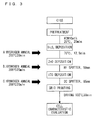
- the stage A herein shows that an annealing treatment (an annealing treatment at 200°C for 20 minutes in a hydrogen atmosphere) is carried out immediately after the formation of the first semiconductor layer 1 (corresponding to In 2 S 3 in Fig. 3 ).
- the stage B shows that the annealing treatment is carried out immediately after the formation of the second semiconductor layer 2 (corresponding to ZnO in Fig. 3 ).
- the stage C shows that the annealing treatment is carried out immediately after the formation of the upper electrode layer 7.
- Table 1 is the result of comparing series resistance values (Rs) for photoelectric conversion elements prepared while varying the timing of the annealing treatment as in Fig. 3 , and a photoelectric conversion element subjected to no annealing treatment.
- the method for measuring the series resistance values (Rs) herein is implemented with electrode terminals placed on the upper electrode layer 7 and the lower electrode layer 5, in which the measurement range was adapted to fall within the range of -1 V to +1 V.
- the resistance value of the photoelectric conversion element subjected to no annealing treatment is regarded as 1 for normalization.
- the Rs in the case of carrying out the annealing treatment is decreased in the order of the stages A, C, and B, showing a tendency that the property is improved in the order of the stages A, C, and B.
- the case of the annealing treatment at the stage of stage B results in a significant decrease in Rs, and thus a notable improvement in property. This is believed to be due to the following reason.
- Fig. 4 shows a photograph of a cross section of the photoelectric conversion element 10 prepared by carrying out the annealing treatment at the stage B.
- the point 1 corresponds to the upper electrode layer 7
- the points 2, 3 correspond to the second semiconductor layer 2
- the points 4, 5 correspond to the first semiconductor layer 1
- the point 6 corresponds to the doped layer region 3
- the point 7 corresponds to the light absorption layer 4. Elemental analysis results for each measurement point are shown below the photograph of the cross section. Thus, it is determined that the doped layer region 3 is formed in a favorable manner.
- Another example of the method for forming the doped layer region 3 will be described.
- An example of a method (referred to as a second method) will be represented now in which the doped layer region 3 is formed by implanting a II-B group element through the first semiconductor layer 1 into the light absorption layer 4, in the formation of the second semiconductor layer 2.
- the light absorption layer 4 and the first semiconductor layer 1 are sequentially formed in the way described above.
- the II-B group element in the second semiconductor layer 2 can be diffused through the first semiconductor layer 1 into the light absorption layer 4 in a favorable manner. This is believed to be due to a pinning effect (implantation effect) produced by the sputtering.
- the composition ratio of the I-B group element may be made lower than the composition ratio of the III-B group element in at least the upper surface portion (on the first semiconductor layer 1 side) of the light absorption layer 4.
- sites on the first semiconductor layer 1 side of the light absorption layer 4 will include a lot of I-B group deficient sites, and the II-B group element will be easily implanted into the I-B group deficient sites of the light absorption layer 4, thereby making it possible to form the doped layer region 3 in a favorable manner.
- a sample of a photoelectric conversion element (device) used in an example of the present invention will be described.
- the lower electrode layer 5 comprised of Mo was deposited by a sputtering method over substantially the entire surface of a cleaned substrate 9.
- a solution of a I-B group metal and a III-B group metal directly dissolved at 20 mass% in a solvent including a chalcogen element containing organic compound and a basic organic solvent was applied by a spin coater onto the surface of the lower electrode layer 5, the drying temperature was adapted to 150°C, and the heat treatment temperature was adapted to 400°C in a nitrogen atmosphere.
- the first semiconductor layer 1 was formed by a CBD method (chemical bath deposition method), and after the first semiconductor layer 1 was formed, a zinc oxide (ZnO) was formed by a sputtering method as the second semiconductor layer 2.
- CBD method chemical bath deposition method
- ZnO zinc oxide
- an indium oxide (ITO) containing tin was formed by a sputtering method as the upper electrode layer 7.
- a conductive paste with a metal powder of Ag dispersed in a resin binder was printed in a pattern shape as the collector electrode 8, and solidified by drying for the formation thereof.
- the diffusion of Zn was achieved by an annealing treatment in a hydrogen atmosphere, which was achieved at a treatment temperature of 300°C for 40 minutes after the formation of the second semiconductor layer.
- a sample corresponding to Patent Document 1 was prepared by diffusing an n-type semiconductor into a light absorption layer of CIGS in the deposition of ZnS as a buffer layer by a CBD method (chemical bath deposition method), and matching the other conditions to the example of the present application (Sample Number 36).
- each sample was subjected to FIB processing, and the cross section was then observed by a TEM to make an EDS analysis of the composition for each stacked section.
- the preparation conditions and evaluation results are shown below in Table 2.
- the conversion efficiency was only on the order of 6% in the case of sample 36 as a comparative example, whereas each sample was able to achieve a higher conversion efficiency in the example of the present invention. This is assumed to be due to the fact that Zn is diffused into the entire light absorption layer 4.
- samples 1 to 5 As long as the thickness of the doped layer region 3 was 5 to 100 nm (samples 2 to 4), the samples achieved adequate p-n junctions, and were able to achieve higher conversion efficiencies without any recombination of carriers, indicating that the samples are more preferable.
- samples 10 to 13 as long as the Cu concentration of the doped layer region 3 was 5 atom% or more (samples 11, 12), the samples were able to achieve desired conversion efficiencies, because Zn is not excessively transferred to the light absorption layer 4.
- samples 14 to 17 As long as the In concentration of the doped layer region 3 was 20 to 30 atom% (samples 15, 16), the samples were able to achieve higher conversion efficiencies, indicating that the samples are more preferable.
- samples 18 to 21 As long as the Ga concentration of the doped layer region 3 was 5 to 15 atom% (samples 19, 20), the samples were able to achieve higher conversion efficiencies, indicating that the samples are more preferable.
- samples 22 to 25 As long as the Se concentration of the doped layer region 3 was 35 to 55 atom% (samples 23, 24), the samples were able to achieve higher conversion efficiencies, indicating that the samples are more preferable.
- samples 26 and 27 were obtained by varying the Cu composition in the light absorption layer from 10 to 20 atom%, and it is determined that the conversion efficiencies are not affected greatly within this range.
- samples 28 to 31 as long as the thickness of the first semiconductor layer 1 is 1 to 30 nm (samples 29, 30), it is easy to transfer Zn from the second semiconductor layer 2 to the light absorption layer 4, and the second semiconductor layer 2 can protect the light absorption layer 4 from stacking damage. Thus, the samples were able to achieve higher conversion efficiencies, indicating that the samples are more preferable.
- samples 32 to 35 as long as the Zn concentration of the first semiconductor layer 1 was 1 to 40 atom% (samples 33, 34), Zn was transferred in just proportion from the second semiconductor layer 2 to the light absorption layer 4, and the samples were able to achieve higher conversion efficiencies, indicating that the samples are more preferable.
Landscapes
- Photovoltaic Devices (AREA)
Abstract
[Problem]
In the case of further stacking a window layer or the like on a buffer layer, the buffer layer and the light absorption layer are likely to be damaged during the formation of the window layer due to inferior moisture resistance and plasma resistance, and photoelectric conversion elements sometimes fail to achieve any satisfactory conversion efficiency in terms of reliability.
[Solving Means]
Provided is a photoelectric conversion element including: a light absorption layer containing a I-B group element, a III-B group element, and a VI-B group element, which is provided on a lower electrode layer; a first semiconductor layer containing a III-B group element and a VI-B group element, which is provided on the light absorption layer; and a second semiconductor layer containing an oxide of a II-B group element, which is provided on the first semiconductor layer, wherein the light absorption layer comprises a doped layer region containing the II-B group element, on the first semiconductor layer side.
Description
- The present invention relates to a photoelectric conversion element, a photoelectric conversion device, and a method for manufacturing a photoelectric conversion element.
- Photoelectric conversion devices for use in solar power generation include photoelectric conversion devices with a light absorption layer made of a chalcopyrite-based I-III-VI group compound semiconductor such as CIGS which has a high light absorption coefficient. The CIGS is suitable for the reduction in film thickness, increase in area, and reduction in cost for photoelectric conversion devices, and research and development have been advanced on next-generation solar cells using this CIGS.
- This type of chalcopyrite-based photoelectric conversion device comprises a configuration with a plurality of photoelectric conversion elements provided adjacent to each other in planar fashion. This photoelectric conversion element is configured by stacking, on substrate such as glass, a lower electrode such as a metal electrode, a photoelectric conversion layer that is a semiconductor layer including a light absorption layer and a buffer layer, and an upper electrode such as a transparent electrode and a metal electrode in this order. Furthermore, the plurality of photoelectric conversion elements are connected electrically in series by electrically connecting the upper electrode of one of adjacent photoelectric conversion elements to the lower electrode of the other photoelectric conversion element through a connecting conductor.
- In recent years, a method has been known in which Zn is diffused directly in a light absorption layer of CIGS. For example, as described in Japanese Patent Application Laid-Open No.
2004-15039 - However, in the case of further stacking a window layer or the like on a buffer layer, the buffer layer of ZnS and the light absorption layer are likely to be damaged during the formation of the window layer due to inferior moisture resistance and plasma resistance of the buffer layer, thereby making it difficult to increase the conversion efficiency of the photoelectric conversion element.
- An object of the present invention is to improve a photoelectric conversion element and a photoelectric conversion device in conversion efficiency.
- A photoelectric conversion element according to an embodiment of the present invention includes: a light absorption layer containing a I-B group element, a III-B group element, and VI-B group element, which is provided on a lower electrode layer; a first semiconductor layer containing a III-B group element and a VI-B group element, which is provided on the light absorption layer; and a second semiconductor layer containing an oxide of a II-B group element, which is provided on the first semiconductor layer, wherein the light absorption layer comprises a doped layer region containing the II-B group element, on the first semiconductor layer side.
- Furthermore, a method for manufacturing a photoelectric conversion element according to an embodiment of the present invention includes a stacking step and a diffusing step. The stacking step is a step of sequentially forming, on a lower electrode layer, a light absorption layer containing a I-B group element, a III-B group element, and a VI-B group element, a first semiconductor layer containing a III-B group element and a VI-B group element, and a second semiconductor layer containing an oxide of a II-B group element. In addition, the diffusing step is a step of diffusing the II-B group element from the second semiconductor layer through the first semiconductor layer to the light absorption layer, after the stacking step.
- Furthermore, a method for manufacturing a photoelectric conversion element according to an embodiment of the present invention includes the following steps. The first step is a step of sequentially forming, on a lower electrode layer, a light absorption layer containing a I-B group element, a III-B group element, and a VI-B group element, and a first semiconductor layer containing a III-B group element and a VI-B group element. The next step is a step of depositing, on the first semiconductor layer, a second semiconductor layer containing an oxide of a II-B group element while implanting the II-B group element through the first semiconductor layer into the light absorption layer.
- Furthermore, a photoelectric conversion device according to an embodiment of the present invention uses the photoelectric conversion element described above.
- The embodiment of the present invention makes it possible to improve the photoelectric conversion element and the photoelectric conversion device in conversion efficiency.
-
-
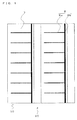
Fig. 1 is a top view illustrating a configuration of a photoelectric conversion device according to the present embodiment. -
Fig. 2 is a cross-sectional pattern diagram of a photoelectric conversion element according to the present embodiment. -
Fig. 3 is a manufacturing process for a photoelectric conversion element according to the present embodiment. -
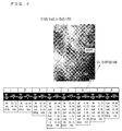
Fig. 4 is a photograph of a cross section of a photoelectric conversion element according to the present embodiment. - An embodiment of the present invention will be described below with reference to the drawings.
- As in
Fig. 1 , aphotoelectric conversion device 20 comprises a configuration including a plurality ofphotoelectric conversion elements 10 provided adjacent to each other on a substrate. - As in
Fig. 2 , eachphotoelectric conversion element 10 mainly includes, on asubstrate 9, alower electrode layer 5, alight absorption layer 4, afirst semiconductor layer 1, asecond semiconductor layer 2, anupper electrode layer 7, and acollector electrode 8 including a collecting section 8a and a connecting section 8b. - In addition, in
Fig. 1 , the principal surface on a side provided with theupper electrodes 7 andcollector electrodes 8 serves as a light receiving surface in thephotoelectric conversion device 20. - The
substrate 9 is intended to support the plurality ofphotoelectric conversion elements 10. Materials to be used for thesubstrate 9 include glass, ceramic, resin, and metal. Blue plate glass (soda lime glass) on the order of 1 to 3 mm in thickness is used here as thesubstrate 9. - The
lower electrode layer 5 is a conductor which is provided on one principal surface of thesubstrate 9 and is comprised of a metal such as Mo, Al, Ti, Ta, or Au or a laminated structure of these metals. Thelower electrode layer 5 is formed to have a thickness on the order of 0.2 to 1 µm with the use of a known thin film formation method such as a sputtering method or a vapor deposition method. - The
light absorption layer 4 is a p-type semiconductor layer mainly containing a chalcopyrite based (hereinafter, also referred to as a CIS based) I-III-VI group compound, which is provided on thelower electrode layer 5. Thislight absorption layer 4 has a thickness on the order of 1 to 3 µm. - The I-III-VI group compound herein refers to a compound of a I-B group element, a III-B group element, and a VI-B group element (in other words, also referred to as a group 11 element, a group 13 element, and a group 16 element), and Cu(In,Ga)Se2 (hereinafter, also referred to as a CIGS) are cited as the present embodiment.
- This
light absorption layer 4 is able to be formed by a so-called vacuum process such as a sputtering method or a vapor deposition method, and additionally, can be also formed by a process referred to as a so-called application method or printing method in which a solution containing a constituent element of thelight absorption layer 4 is applied onto thelower electrode layer 5, and then subjected to drying and a heat treatment. - The
first semiconductor layer 1 is a semiconductor layer having an n-type conductivity type and containing a III-B group element and a VI-B group element, which is provided on thelight absorption layer 4. - The
first semiconductor layer 1 is provided in the form of heterojunction with thelight absorption layer 4, when thelight absorption layer 4 is comprised of a I-III-VI group compound semiconductor. Thus, when thesecond semiconductor layer 2 is formed on thefirst semiconductor layer 1, thelight absorption layer 4 can be protected from damage. - Furthermore, the
first semiconductor layer 1 may be formed by a CBD method (chemical bath deposition method) to have a thickness of, for example, 1 to 30 nm. This can diffuse a II-B group element from thesecond semiconductor layer 2 to thelight absorption layer 4 to stably form a dopedlayer region 3 on the surface of thelight absorption layer 4. - Furthermore, examples of the III-B group element contained in the
first semiconductor layer 1 include In, Ga, etc. In addition, examples of the VI-B group element contained in thefirst semiconductor layer 1 include S, etc. - Furthermore, the
first semiconductor layer 1 contains the II-B group element, and the concentration of the II-B group element in thefirst semiconductor layer 1 is higher on thesecond semiconductor layer 2 side than on the lightabsorption layer side 4. This improves the efficiency of the electrical junction between thefirst semiconductor layer 1 and thesecond semiconductor layer 2, and can match thefirst semiconductor layer 1 and thelight absorption layer 4 in terms of lattice constant to reduce lattice defects. - Furthermore, the concentration of the II-B group element is supposed to be 1 to 40 atom% in the entire
first semiconductor layer 1. The concentration of the II-B group element in the entirefirst semiconductor layer 1 herein refers to an average value in the case of performing a quantitative analysis in the thickness direction for thefirst semiconductor layer 1 by an EDS analysis or the like. Thus, further diffusion of the II-B group element from thesecond semiconductor layer 2 into the dopedlayer region 3 can be reduced during the use of thephotoelectric conversion device 1. More specifically, thefirst semiconductor layer 1 can act to buffer the diffusion of the II-B group element, and stably maintain the p-n junction formed in thelight absorption layer 4. - In addition, the
first semiconductor layer 1 may contain oxygen (O) in the state of an oxide and/or a hydroxide. When thefirst semiconductor layer 1 contains O and S, the O concentration may be lower on thelight absorption layer 4 side of thefirst semiconductor layer 1 than on thesecond semiconductor layer 2 side of thefirst semiconductor layer 1. Thus, thefirst semiconductor layer 1 on thelight absorption layer 4 side has, as a result, a higher S proportion in place of O in the same group, so that the lattice constant can be made closer to that of thelight absorption layer 4, thus improving the electrical junction between thelight absorption layer 4 and thefirst semiconductor layer 1. - This
first semiconductor layer 1 with a site different in O concentration can be prepared by, for example, a method such as changing the pH or S concentration in preparing thefirst semiconductor layer 1 by a CBD method. - In addition, when the O proportion is higher on the
second semiconductor layer 2 side of thefirst semiconductor layer 1, the structures of In2O3 and In(OH)3 may be increased on thesecond semiconductor layer 2 side. These structures can make a contribution to an improvement in conversion efficiency, because of their wider band gaps than that of In2S3. - The
second semiconductor layer 2 is a semiconductor layer having an n-type conductivity type and containing an oxide of a II-B group element, which is provided on thefirst semiconductor layer 1. - Examples of the oxide of the II-B group element, which is contained in the
second semiconductor layer 2, include, for example, a zinc oxide (ZnO) and a cadmium oxide (CdO). Thesecond semiconductor layer 2 may be formed by a sputtering method, a vapor deposition method, etc. - The existence of this
second semiconductor layer 2 reduces the generation of a leakage current between theupper electrode layer 7 and thelight absorption layer 4. - Now, although a difference is produced between the explanation order and the stacking order, an embodiment of the present invention comprises the doped
layer region 3 containing a II-B group element on thefirst semiconductor layer 1 side of thelight absorption layer 4 as inFig. 2 . Examples of the II-B group element contained in the dopedlayer region 3 include Zn, Cd, etc. The dopedlayer region 3 containing the II-B group element serves as the n-type conductive layer in thelight absorption layer 4, and a favorable p-n junction is thus formed in thelight absorption layer 4. Therefore, the photoelectric conversion efficiency of the photoelectric conversion element is further improved. - Furthermore, when the thickness of the doped
layer region 3 is 5 to 100 nm, the recombination of photogenerated carriers can be relatively reduced. - For example, when In2S3 is used for the
first semiconductor layer 1, whereas ZnO is deposited as thesecond semiconductor layer 2, the n-type dopedlayer region 3 formed by doping thefirst semiconductor layer 1 side of thelight absorption layer 4 with Zn, forms a p-n homojunction with thelight absorption layer 4, provides more stability, and increases the conversion efficiency. - In this case, as long as the concentration of Zn in the doped
layer region 3 is 1 to 30 atom%, the p-n junction is stabilized to increase the conversion efficiency, and the recombination of photogenerated carriers can be relatively reduced. - Furthermore, as long as the concentration of the I-B group element in the doped
layer region 3 is lower than the concentration of the I-B group element in the other entire region of thelight absorption layer 4, the deficiency of the I-B group element in the I-B group element makes the II-B group element more likely to be located at the site of the deficiency in I-B group element, thereby promoting the n-type of the dopedlayer region 3, stabilizing the p-n junction, and increasing the conversion efficiency. - When the
light absorption layer 4 contains Cu as the I-B group element, contains In and Ga as the III-B group element, and contains Se as the VI-B group element, the concentrations of Cu, In, Ga, and Se in the dopedlayer region 3 may be respectively 5 atom% or more for Cu, 20 to 30 atom% for In, 5 to 15 atom% for Ga, and 35 to 55 atom% for Se. Thus, a p-n junction can be formed in a favorable manner in thelight absorption layer 4. - The
upper electrode layer 7 is an n-type transparent conductive film provided on thesecond semiconductor layer 2. Theupper electrode layer 7 is provided as an electrode for extracting charges generated in photoelectric conversion through thesecond semiconductor layer 2. - In addition, the
upper electrode layer 7 is comprised of a substance which has a lower resistivity than those of thefirst semiconductor layer 1 and thesecond semiconductor layer 2, for example, an indium oxide (ITO) containing tin, or the like. Theupper electrode layer 7 is formed by a sputtering method, a vapor deposition method, or the like. - It is to be noted that the
first semiconductor layer 1, thesecond semiconductor layer 2, and theupper electrode layer 7 may be comprised of substances which have a light transmitting property with respect to the wavelength range of light absorbed by thelight absorption layer 4. In addition, as long as thefirst semiconductor layer 1, thesecond semiconductor layer 2, and theupper electrode layer 7 have substantially the same absolute refractive index, the light absorption efficiency in thelight absorption layer 4 is further improved. - The
collector electrode 8 is comprised of the collecting section 8a and the connecting section 8b which are comprised of a metal such as Ag, and has a role in collecting charges generated in thephotoelectric conversion element 10 and extracted in theupper electrode layer 7. This makes it possible to reduce theupper electrode layer 7 in thickness. - The
collector electrode 8 may have a width of 50 to 400 µm in consideration of conductivity and light transmission to thelight absorption layer 4. - Next, a photoelectric conversion element and a photoelectric conversion device according to another embodiment of the present invention will be described.
- In the photoelectric conversion element and the photoelectric conversion device, the
second semiconductor layer 2 may further contain therein hydrogen (H). This can compensate lattice defects in thesecond semiconductor layer 2 with the H, and the power generation efficiency can be thus improved. - In addition, the
first semiconductor layer 1 may contain therein H. This can compensate lattice defects in thefirst semiconductor layer 1 with the H, and the power generation efficiency can be thus improved. - In addition, the
light absorption layer 4 may contain therein H. This can compensate lattice defects in thelight absorption layer 4 with the H, and the power generation efficiency can be thus improved. - For these
second semiconductor layer 2 containing H,first semiconductor layer 1 containing H, andlight absorption layer 4 containing H, each layer can be doped with H by carrying out an annealing treatment in a hydrogen atmosphere. - Next, a process for manufacturing a photoelectric conversion device which comprises the structure described above will be described.
- A case of forming the
light absorption layer 4 comprised of a I-III-VI group compound semiconductor (for example, a CIGS including Cu, In, Ga, and Se, or the like) by using an application method, and further forming thefirst semiconductor layer 1 and the subsequent layers will be described below as an example. - First, the
lower electrode layer 5 comprised of Mo is deposited by a sputtering method over substantially the entire surface of a cleanedsubstrate 1. Thelight absorption layer 4 and thefirst semiconductor layer 1 are sequentially formed on thelower electrode layer 5. - Next, after the
lower electrode layer 5 is formed, a solution for forming thelight absorption layer 4 is applied to the surface of thelower electrode layer 5, and subjected to drying to form a coating, and the coating is subjected to a heat treatment to form thelight absorption layer 4. - The solution for forming the
light absorption layer 4 is prepared by dissolving a I-B group metal and a III-group metal directly in a solvent including a chalcogen element containing organic compound and a basic organic solvent, and supposed to be a solution in which the total concentration of the I-B group metal and III-group metal is 10 mass% or more. It is to be noted that it is possible to apply various methods such as a spin coater, screen printing, dipping, a spray, and a die coater, for the application of the solution. - The chalcogen element containing organic compound refers to an organic compound containing a chalcogen element. The chalcogen element refers to S, Se, or Te among the VI-B group elements. Examples of the chalcogen element containing organic compound include, for example, thiol, sulfide, selenol, and terenol. Dissolving a metal directly in a mixed solvent refers to mixing and dissolving a metal alone or raw metal of an alloy directly in a mixed solvent.
- The drying is carried out, for example, under a reducing atmosphere. The drying temperature is, for example, 50 to 300°C. The heat treatment is carried out, for example, under a reducing atmosphere of a hydrogen atmosphere. The heat treatment temperature is, for example, 400 to 600°C.
- Next, after the
light absorption layer 4 is formed, thefirst semiconductor layer 1 is formed by a CBD method (a chemical bath deposition method). The thickness of thefirst semiconductor layer 1 can be a thickness to an extent that, for example, allow easy passage of the II-B group element (for example, Zn) for forming the dopedlayer region 3, and can protect thelight absorption layer 4 from damage by sputtering in a subsequent step. - Next, after the
first semiconductor layer 1 is formed, for example, a zinc oxide (ZnO) is formed by a sputtering method, a vapor deposition method, or the like, as thesecond semiconductor layer 2. - Next, after the
second semiconductor layer 2 is formed, an indium oxide containing tin (ITO) or the like is formed by a sputtering method, a vapor deposition method, or the like as theupper electrode layer 7. - After the
upper electrode layer 7 is formed, a conductive paste with a metal powder such as Ag dispersed in a resin binder or the like is printed in a pattern shape as thecollector electrode 8, and solidified by drying for the formation thereof. - A method for forming the doped
layer region 3 will be described below in an embodiment of the present invention. First, an example of a method (referred to as a first method) will be represented below in which the dopedlayer region 3 is formed by diffusing Zn contained in thesecond semiconductor layer 2 through thefirst semiconductor layer 1 into thelight absorption layer 4. - As represented by the method for manufacturing the photoelectric conversion element, the
light absorption layer 4, thefirst semiconductor layer 1, and thesecond semiconductor layer 2 are formed sequentially on the lower electrode layer (hereinafter, referred to as a stacking step). Then, after this stacking step, the II-B group element is diffused from thesecond semiconductor layer 2 through thefirst semiconductor layer 1 into the light absorption layer 4 (hereinafter, referred to as a diffusing step). - The diffusing step is carried out by an annealing treatment to the
second semiconductor layer 2. From the viewpoint that the II-B group element is easily diffused, the composition ratio of the I-B group element may be made lower than the composition ratio of the III-B group element in at least the upper surface portion (on thefirst semiconductor layer 1 side) of thelight absorption layer 4 formed in the stacking step. Thus, sites on thefirst semiconductor layer 1 side of thelight absorption layer 4 will include a lot of I-B group deficient sites, and the II-B group element will easily diffuse to the I-B group deficient sites of thelight absorption layer 4, thereby making it possible to form the dopedlayer region 3 in a favorable manner. - A method for forming the
light absorption layer 4 will be represented below in which these sites on thefirst semiconductor layer 1 side of thelight absorption layer 4 include I-B group element deficient sites. - First, in the heat treatment of the coating formed by applying a solution for forming the
light absorption layer 4, the coating is kept at a relatively low temperature (100 to 400°C). Thus, the metal complex constituting the coating undergoes liquefaction by melting, and the organic constituent evaporates gradually. In this case, the I-B group element which has a relatively smaller solubility in the liquid metal complex than the other elements (III-B group elements and VI-B group elements) shows a tendency to be transferred to one principal surface side of thelower electrode layer 5 for preferential deposition. As a result, thelight absorption layer 4 with Cu deficient sites can be formed on thefirst semiconductor layer 1 side. - Alternatively, the solution for forming the
light absorption layer 4 may be applied in more than once, so that the I-B group element concentration of the solution applied last may be lowered. - In addition, the annealing treatment in the diffusing step may be carried out in a hydrogen atmosphere. This can diffuse the II-B group element of the
second semiconductor layer 2 more easily, and prepare the dopedlayer region 3 easily. This is believed to be because the diffusion of the II-B group element is facilitated due to the fact that the bond between the mutually bonded II-B group element and oxygen is broken by hydrogen to isolate the II-B group element in thesecond semiconductor layer 2. - An example of a process for manufacturing the
photoelectric conversion element 10 is shown inFig. 3 herein. In this process, the timing of an annealing treatment in a hydrogen atmosphere includes stages A, B, and C shown inFig. 3 . The stage A herein shows that an annealing treatment (an annealing treatment at 200°C for 20 minutes in a hydrogen atmosphere) is carried out immediately after the formation of the first semiconductor layer 1 (corresponding to In2S3 inFig. 3 ). In addition, the stage B shows that the annealing treatment is carried out immediately after the formation of the second semiconductor layer 2 (corresponding to ZnO inFig. 3 ). In addition, the stage C shows that the annealing treatment is carried out immediately after the formation of theupper electrode layer 7. - Table 1 is the result of comparing series resistance values (Rs) for photoelectric conversion elements prepared while varying the timing of the annealing treatment as in
Fig. 3 , and a photoelectric conversion element subjected to no annealing treatment. The method for measuring the series resistance values (Rs) herein is implemented with electrode terminals placed on theupper electrode layer 7 and thelower electrode layer 5, in which the measurement range was adapted to fall within the range of -1 V to +1 V. In Table 1, the resistance value of the photoelectric conversion element subjected to no annealing treatment is regarded as 1 for normalization. -
[Table 1] Resistance Value (Ratio) With no Hydrogen Anneal 1 With Hydrogen Anneal (Stage A) 0.72 With Hydrogen Anneal (Stage B) 0.64 With Hydrogen Anneal (Stage C) 0.07 - According to Table 1, as compared with the case of carrying out no annealing treatment, that is, the case without the doped
layer region 3 formed, the Rs in the case of carrying out the annealing treatment is decreased in the order of the stages A, C, and B, showing a tendency that the property is improved in the order of the stages A, C, and B. In particular, the case of the annealing treatment at the stage of stage B results in a significant decrease in Rs, and thus a notable improvement in property. This is believed to be due to the following reason. While the diffusion of Zn from thesecond semiconductor layer 2 is caused a decrease in Rs in each of the annealing treatment at the stage B and the annealing treatment at the stage C, the Zn in thesecond semiconductor layer 2 is more likely to be isolated by hydrogen in the atmosphere particularly in the annealing treatment at the stage B. Therefore, it is believed that this isolated Zn diffuses to form the dopedlayer region 3 in thelight absorption layer 4 in a favorable manner. - It is to be noted that
Fig. 4 shows a photograph of a cross section of thephotoelectric conversion element 10 prepared by carrying out the annealing treatment at the stage B. For respective circled measurement points shown inFig. 4 , thepoint 1 corresponds to theupper electrode layer 7, thepoints second semiconductor layer 2, thepoints first semiconductor layer 1, thepoint 6 corresponds to the dopedlayer region 3, and thepoint 7 corresponds to thelight absorption layer 4. Elemental analysis results for each measurement point are shown below the photograph of the cross section. Thus, it is determined that the dopedlayer region 3 is formed in a favorable manner. - Another example of the method for forming the doped
layer region 3 will be described. An example of a method (referred to as a second method) will be represented now in which the dopedlayer region 3 is formed by implanting a II-B group element through thefirst semiconductor layer 1 into thelight absorption layer 4, in the formation of thesecond semiconductor layer 2. - First, the
light absorption layer 4 and thefirst semiconductor layer 1 are sequentially formed in the way described above. Next, in the formation of thesecond semiconductor layer 2, on the condition that the ion implantation intensity of sputtering is increased, the II-B group element in thesecond semiconductor layer 2 can be diffused through thefirst semiconductor layer 1 into thelight absorption layer 4 in a favorable manner. This is believed to be due to a pinning effect (implantation effect) produced by the sputtering. - In this case, from the viewpoint that the II-B group element is easily implanted into the
light absorption layer 4, the composition ratio of the I-B group element may be made lower than the composition ratio of the III-B group element in at least the upper surface portion (on thefirst semiconductor layer 1 side) of thelight absorption layer 4. Thus, sites on thefirst semiconductor layer 1 side of thelight absorption layer 4 will include a lot of I-B group deficient sites, and the II-B group element will be easily implanted into the I-B group deficient sites of thelight absorption layer 4, thereby making it possible to form the dopedlayer region 3 in a favorable manner. - For a method for forming the foregoing
light absorption layer 4 in which sites on thefirst semiconductor layer 1 side of thelight absorption layer 4 include I-B group element deficient sites, the method represented by the first method can be adopted. Example - A sample of a photoelectric conversion element (device) used in an example of the present invention will be described.
- First, the
lower electrode layer 5 comprised of Mo was deposited by a sputtering method over substantially the entire surface of a cleanedsubstrate 9. - Next, for the
light absorption layer 4, a solution of a I-B group metal and a III-B group metal directly dissolved at 20 mass% in a solvent including a chalcogen element containing organic compound and a basic organic solvent was applied by a spin coater onto the surface of thelower electrode layer 5, the drying temperature was adapted to 150°C, and the heat treatment temperature was adapted to 400°C in a nitrogen atmosphere. - The
first semiconductor layer 1 was formed by a CBD method (chemical bath deposition method), and after thefirst semiconductor layer 1 was formed, a zinc oxide (ZnO) was formed by a sputtering method as thesecond semiconductor layer 2. - After the
second semiconductor layer 2 was formed, an indium oxide (ITO) containing tin was formed by a sputtering method as theupper electrode layer 7. - After the
upper electrode layer 7 was formed, a conductive paste with a metal powder of Ag dispersed in a resin binder was printed in a pattern shape as thecollector electrode 8, and solidified by drying for the formation thereof. - Then, the diffusion of Zn was achieved by an annealing treatment in a hydrogen atmosphere, which was achieved at a treatment temperature of 300°C for 40 minutes after the formation of the second semiconductor layer.
- As a comparative example, a sample corresponding to Patent
Document 1 was prepared by diffusing an n-type semiconductor into a light absorption layer of CIGS in the deposition of ZnS as a buffer layer by a CBD method (chemical bath deposition method), and matching the other conditions to the example of the present application (Sample Number 36). - For each of these
photoelectric conversion devices 20, the conversion efficiency was measured. As for the method for composition analysis, each sample was subjected to FIB processing, and the cross section was then observed by a TEM to make an EDS analysis of the composition for each stacked section. The preparation conditions and evaluation results are shown below in Table 2. -
[Table 21 Sample Number Zn Doped Layer Light Absorption Layer First Semiconductor Layer Conversion Efficiency Thickness Zn Concentration Cu Concentration In Concentration Ga Concentration Se Concentration Cu Concentration Thickness Zn concentration nm atom% atom% atom% atom% atom% atom% nm atom% % 1 4 15 10 25 10 45 15 0.5 20 9 2 5 15 10 25 10 45 15 1 20 11 3 50 15 10 25 10 45 15 15 20 11 4 100 15 10 25 10 45 15 30 20 10 5 200 15 10 25 10 45 15 30 20 9 6 50 0.5 10 25 10 45 15 40 20 9 7 50 1 10 25 10 45 15 15 20 10 8 50 30 10 25 10 45 15 15 20 10 9 50 40 10 25 10 45 15 15 20 9 10 50 15 4 25 10 45 15 15 20 9 11 50 15 5 25 10 45 15 15 20 10 12 50 15 25 25 10 45 15 15 20 10 13 50 15 30 25 10 45 15 15 20 9 14 50 15 10 15 10 45 15 15 20 10 15 50 15 10 20 10 45 15 15 20 11 16 50 15 10 30 10 45 15 15 20 11 17 50 15 10 35 10 45 15 15 20 10 18 50 15 10 25 4 45 15 15 20 9 19 50 15 10 25 5 45 15 15 20 10 20 50 15 10 25 15 45 15 15 20 10 21 50 15 10 25 20 45 15 15 20 9 22 50 15 10 25 10 30 15 15 20 8 23 50 15 10 25 10 35 15 15 20 9 24 50 15 10 25 10 55 15 15 20 11 25 50 15 10 25 10 60 15 15 20 10 26 50 15 10 25 10 45 10 15 20 10 27 50 15 10 25 10 45 20 15 20 12 28 50 15 10 25 10 45 15 0.5 20 10 29 50 15 10 25 10 45 15 1 20 11 30 50 15 10 25 10 45 15 30 20 9 31 50 15 10 25 10 45 15 40 20 8 32 50 15 10 25 10 45 15 15 0.5 10 33 50 15 10 25 10 45 15 15 1 11 34 50 15 10 25 10 45 15 15 40 11 35 50 15 10 25 10 45 15 15 50 10 36 Zn Diffusion into Entire Light Absorption Layer 15 15 20 6 - The conversion efficiency was only on the order of 6% in the case of sample 36 as a comparative example, whereas each sample was able to achieve a higher conversion efficiency in the example of the present invention. This is assumed to be due to the fact that Zn is diffused into the entire
light absorption layer 4. - In the case of
samples 1 to 5, as long as the thickness of the dopedlayer region 3 was 5 to 100 nm (samples 2 to 4), the samples achieved adequate p-n junctions, and were able to achieve higher conversion efficiencies without any recombination of carriers, indicating that the samples are more preferable. - In the case of
samples 6 to 9, as long as the Zn concentration near the center of the dopedlayer region 3 was 1 to 30 atom% (7, 8), the samples achieved adequate p-n junctions, and were able to achieve higher conversion efficiencies without any recombination of carriers, indicating that the samples are more preferable. - In the case of
samples 10 to 13, as long as the Cu concentration of the dopedlayer region 3 was 5 atom% or more (samples 11, 12), the samples were able to achieve desired conversion efficiencies, because Zn is not excessively transferred to thelight absorption layer 4. - In the case of samples 14 to 17, as long as the In concentration of the doped
layer region 3 was 20 to 30 atom% (samples 15, 16), the samples were able to achieve higher conversion efficiencies, indicating that the samples are more preferable. - In the case of samples 18 to 21, as long as the Ga concentration of the doped
layer region 3 was 5 to 15 atom% (samples 19, 20), the samples were able to achieve higher conversion efficiencies, indicating that the samples are more preferable. - In the case of samples 22 to 25, as long as the Se concentration of the doped
layer region 3 was 35 to 55 atom% (samples 23, 24), the samples were able to achieve higher conversion efficiencies, indicating that the samples are more preferable. - In the case of samples 26 and 27, the samples were obtained by varying the Cu composition in the light absorption layer from 10 to 20 atom%, and it is determined that the conversion efficiencies are not affected greatly within this range.
- In the case of samples 28 to 31, as long as the thickness of the
first semiconductor layer 1 is 1 to 30 nm (samples 29, 30), it is easy to transfer Zn from thesecond semiconductor layer 2 to thelight absorption layer 4, and thesecond semiconductor layer 2 can protect thelight absorption layer 4 from stacking damage. Thus, the samples were able to achieve higher conversion efficiencies, indicating that the samples are more preferable. - In the case of samples 32 to 35, as long as the Zn concentration of the
first semiconductor layer 1 was 1 to 40 atom% (samples 33, 34), Zn was transferred in just proportion from thesecond semiconductor layer 2 to thelight absorption layer 4, and the samples were able to achieve higher conversion efficiencies, indicating that the samples are more preferable. - It is to be noted that the present invention is not limited to the embodiments described above and is also intended to encompass any combination of the embodiments described above.
-
- 1:
- first semiconductor layer
- 2:
- second semiconductor layer
- 3:
- doped layer region
- 4:
- light absorption layer
- 5:
- lower electrode layer
- 7:
- upper electrode layer
- 8:
- collector electrode
- 8a:
- collecting section
- 8b:
- connecting section
- 9:
- substrate
- 10:
- photoelectric conversion element
- 20:
- photoelectric conversion device
Claims (13)
- A photoelectric conversion element comprising:a light absorption layer containing a I-B group element, a III-B group element, and a VI-B group element, which is provided on a lower electrode layer;a first semiconductor layer containing a III-B group element and a VI-B group element, which is provided on the light absorption layer; anda second semiconductor layer containing an oxide of a II-B group element, which is provided on the first semiconductor layer,wherein the light absorption layer comprises a doped layer region containing the II-B group element, on the first semiconductor layer side.
- The photoelectric conversion element according to claim 1, wherein a thickness of the doped layer region is 5 to 100 nm.
- The photoelectric conversion element according to claim 1 or 2, wherein the first semiconductor layer comprises In and S, the second semiconductor layer comprises ZnO, and the doped layer region comprises Zn.
- The photoelectric conversion element according to claim 3, wherein a Zn concentration in the doped layer region is 1 to 30 atom%.
- The photoelectric conversion element according to any of claims 1 to 4, wherein the light absorption layer comprises Cu as a I-B group element, comprises In and Ga as III-B group elements, and comprises Se as a VI-B group element,
concentrations of Cu, In, Ga, and Se in the doped layer region are respectively 5 atom% or more for the Cu, 20 to 30 atom% for the In, 5 to 15 atom% for the Ga, and 35 to 55 atom% for the Se. - The photoelectric conversion element according to any of claims 1 to 5, wherein a thickness of the first semiconductor layer is 1 to 30 nm.
- The photoelectric conversion element according to any of claims 1 to 6, wherein the first semiconductor layer comprises a II-B group element, and
a concentration of the II-B group element is higher on the second semiconductor layer side than on the light absorption layer side in the first semiconductor layer. - The photoelectric conversion element according to claim 7, wherein the concentration of the II-B group element is 1 to 40 atom% in the entire first semiconductor layer.
- A photoelectric conversion device using the photoelectric conversion element according to any of claims 1 to 8.
- A method for manufacturing a photoelectric conversion element comprising: a stacking step of sequentially forming, on a lower electrode layer, a light absorption layer containing a I-B group element, a III-B group element, and a VI-B group element, a first semiconductor layer containing a III-B group element and a VI-B group element, and a second semiconductor layer containing an oxide of a II-B group element; and
a diffusing step of diffusing the II-B group element from the second semiconductor layer through the first semiconductor layer to the light absorption layer, after the stacking step. - The method for manufacturing a photoelectric conversion element according to claim 10, wherein the diffusing step is a step of subjecting the second semiconductor layer to an annealing treatment in a hydrogen atmosphere.
- A method for manufacturing a photoelectric conversion element comprising: a stacking step of sequentially forming, on a lower electrode layer, a light absorption layer containing a I-B group element, a III-B group element, and a VI-B group element, and a first semiconductor layer containing a III-B group element and a VI-B group element; and
a deposition step of depositing, on the first semiconductor layer, a second semiconductor layer containing an oxide of a II-B group element while implanting the II-B group element through the first semiconductor layer into the light absorption layer. - The method for manufacturing a photoelectric conversion element according to claim 12, wherein a layer in which a composition ratio of the I-B group element is lower than a composition ratio of the III-B group element in at least a surface portion on a side opposite to the lower electrode layer is formed as the light absorption layer in the stacking step, and
the second semiconductor layer is formed by sputtering in the deposition step.
Applications Claiming Priority (4)
| Application Number | Priority Date | Filing Date | Title |
|---|---|---|---|
| JP2010102517 | 2010-04-27 | ||
| JP2010120084 | 2010-05-26 | ||
| JP2010242990 | 2010-10-29 | ||
| PCT/JP2011/060216 WO2011136249A1 (en) | 2010-04-27 | 2011-04-27 | Photoelectric conversion element, photoelectric conversion device, and method for manufacturing photoelectric conversion element |
Publications (2)
| Publication Number | Publication Date |
|---|---|
| EP2565939A1 true EP2565939A1 (en) | 2013-03-06 |
| EP2565939A4 EP2565939A4 (en) | 2014-04-23 |
Family
ID=44861547
Family Applications (1)
| Application Number | Title | Priority Date | Filing Date |
|---|---|---|---|
| EP11775030.7A Withdrawn EP2565939A4 (en) | 2010-04-27 | 2011-04-27 | PHOTOELECTRIC CONVERSION ELEMENT, PHOTOELECTRIC CONVERSION DEVICE, AND METHOD FOR MANUFACTURING PHOTOELECTRIC CONVERSION ELEMENT |
Country Status (5)
| Country | Link |
|---|---|
| US (1) | US20130032201A1 (en) |
| EP (1) | EP2565939A4 (en) |
| JP (1) | JPWO2011136249A1 (en) |
| CN (1) | CN102859720A (en) |
| WO (1) | WO2011136249A1 (en) |
Families Citing this family (6)
| Publication number | Priority date | Publication date | Assignee | Title |
|---|---|---|---|---|
| JP2013106013A (en) * | 2011-11-16 | 2013-05-30 | Toshiba Corp | Photoelectric conversion element and solar cell |
| JP5878416B2 (en) * | 2012-03-30 | 2016-03-08 | 本田技研工業株式会社 | Chalcopyrite solar cell and method for manufacturing the same |
| JP6312996B2 (en) * | 2012-09-26 | 2018-04-18 | 株式会社東芝 | Photoelectric conversion element and solar cell |
| CN106531827A (en) * | 2015-09-15 | 2017-03-22 | 株式会社东芝 | Photoelectric conversion element, solar cell, solar cell module, and solar power generating system |
| JP2017059657A (en) * | 2015-09-16 | 2017-03-23 | 株式会社東芝 | Photoelectric conversion element and solar cell |
| CN109716261A (en) | 2016-07-29 | 2019-05-03 | 寇平公司 | Mobile device shell |
Family Cites Families (6)
| Publication number | Priority date | Publication date | Assignee | Title |
|---|---|---|---|---|
| US5948176A (en) * | 1997-09-29 | 1999-09-07 | Midwest Research Institute | Cadmium-free junction fabrication process for CuInSe2 thin film solar cells |
| US6441301B1 (en) * | 2000-03-23 | 2002-08-27 | Matsushita Electric Industrial Co., Ltd. | Solar cell and method of manufacturing the same |
| JP4320529B2 (en) | 2002-06-05 | 2009-08-26 | 本田技研工業株式会社 | Compound thin film solar cell and manufacturing method thereof |
| ATE467909T1 (en) * | 2004-01-13 | 2010-05-15 | Panasonic Corp | SOLAR CELL AND PRODUCTION PROCESS |
| DE102007023697A1 (en) * | 2006-05-25 | 2007-12-06 | Honda Motor Co., Ltd. | Chalcopyrite solar cell for converting light into electricity, has contact electrode with conductivity, which is higher than that of light absorption layer, and upper electrode divided into parts in area adjacent to contact electrode |
| JP2008235794A (en) * | 2007-03-23 | 2008-10-02 | Tokyo Univ Of Science | Photoelectric conversion material, method for producing the same, semiconductor element, and solar cell |
-
2011
- 2011-04-27 WO PCT/JP2011/060216 patent/WO2011136249A1/en not_active Ceased
- 2011-04-27 CN CN2011800199698A patent/CN102859720A/en active Pending
- 2011-04-27 EP EP11775030.7A patent/EP2565939A4/en not_active Withdrawn
- 2011-04-27 US US13/642,043 patent/US20130032201A1/en not_active Abandoned
- 2011-04-27 JP JP2012512871A patent/JPWO2011136249A1/en active Pending
Non-Patent Citations (3)
| Title |
|---|
| POWALLA M ET AL: "Scaling up issues of CIGS solar cells", THIN SOLID FILMS, ELSEVIER-SEQUOIA S.A. LAUSANNE, CH, vol. 361-362, no. 1, 1 February 2000 (2000-02-01), pages 540-546, XP004187534, ISSN: 0040-6090, DOI: 10.1016/S0040-6090(99)00849-4 * |
| See also references of WO2011136249A1 * |
| SPIERING S ET AL: "Large-area Cd-free CIGS solar modules with In2S3 buffer layer deposited by ALCVD", THIN SOLID FILMS, ELSEVIER-SEQUOIA S.A. LAUSANNE, CH, vol. 451-452, 22 March 2004 (2004-03-22), pages 562-566, XP004495165, ISSN: 0040-6090, DOI: 10.1016/J.TSF.2003.10.090 * |
Also Published As
| Publication number | Publication date |
|---|---|
| JPWO2011136249A1 (en) | 2013-07-22 |
| CN102859720A (en) | 2013-01-02 |
| EP2565939A4 (en) | 2014-04-23 |
| US20130032201A1 (en) | 2013-02-07 |
| WO2011136249A1 (en) | 2011-11-03 |
Similar Documents
| Publication | Publication Date | Title |
|---|---|---|
| KR101144810B1 (en) | Electrode paste for solar cell, solar cell using the paste, and manufacturing method of the solar cell | |
| US7632701B2 (en) | Thin film solar cells by selenization sulfurization using diethyl selenium as a selenium precursor | |
| US8653616B2 (en) | Photoelectric conversion device | |
| JP2011155237A (en) | Compound thin film solar cell, method of manufacturing compound thin film solar cell, and compound thin film solar cell module | |
| US9023680B2 (en) | Method for producing compound semiconductor, method for manufacturing photoelectric conversion device, and solution for forming semiconductor | |
| EP2565939A1 (en) | Photoelectric conversion element, photoelectric conversion device, and method for manufacturing photoelectric conversion element | |
| EP2600412B1 (en) | Photoelectric conversion device | |
| EP2768030A2 (en) | Solar cell and method of manufacturing the same | |
| US8772826B2 (en) | Photoelectric conversion device | |
| WO2011149008A1 (en) | Photoelectric conversion device and method for manufacturing a photoelectric conversion device | |
| US8709860B2 (en) | Method for manufacturing photoelectric conversion device | |
| JP5623311B2 (en) | Photoelectric conversion device | |
| US20130240948A1 (en) | Photoelectric conversion device | |
| KR101610382B1 (en) | Solar cell and method of fabricating the same | |
| KR101162162B1 (en) | Electrode paste for solar cell, solar cell using the paste, and manufacturing method of the solar cell | |
| US20140224333A1 (en) | Photoelectric conversion device | |
| KR20150057807A (en) | Solar cell and method for manufacturing the same | |
| JP2011249560A (en) | Semiconductor layer manufacturing method and photoelectric conversion device manufacturing method | |
| KR20130064656A (en) | Method of fabricating solar cell | |
| WO2012115267A1 (en) | Photoelectric conversion element and photoelectric conversion device | |
| JP2012109558A (en) | Photoelectric conversion element, photoelectric conversion device, and method of manufacturing photoelectric conversion element | |
| JPH0738128A (en) | Solar cell | |
| JP2011151182A (en) | Photoelectric conversion apparatus, and method of manufacturing the same | |
| JP2014011269A (en) | Photoelectric conversion device and method of manufacturing the same |
Legal Events
| Date | Code | Title | Description |
|---|---|---|---|
| PUAI | Public reference made under article 153(3) epc to a published international application that has entered the european phase |
Free format text: ORIGINAL CODE: 0009012 |
|
| 17P | Request for examination filed |
Effective date: 20121017 |
|
| AK | Designated contracting states |
Kind code of ref document: A1 Designated state(s): AL AT BE BG CH CY CZ DE DK EE ES FI FR GB GR HR HU IE IS IT LI LT LU LV MC MK MT NL NO PL PT RO RS SE SI SK SM TR |
|
| DAX | Request for extension of the european patent (deleted) | ||
| A4 | Supplementary search report drawn up and despatched |
Effective date: 20140325 |
|
| RIC1 | Information provided on ipc code assigned before grant |
Ipc: H01L 31/072 20120101AFI20140319BHEP |
|
| STAA | Information on the status of an ep patent application or granted ep patent |
Free format text: STATUS: THE APPLICATION HAS BEEN WITHDRAWN |
|
| 18W | Application withdrawn |
Effective date: 20140424 |