EP2564435B1 - Method for fabricating a light emitting diode with a laminated phosphor layer - Google Patents
Method for fabricating a light emitting diode with a laminated phosphor layer Download PDFInfo
- Publication number
- EP2564435B1 EP2564435B1 EP11722561.5A EP11722561A EP2564435B1 EP 2564435 B1 EP2564435 B1 EP 2564435B1 EP 11722561 A EP11722561 A EP 11722561A EP 2564435 B1 EP2564435 B1 EP 2564435B1
- Authority
- EP
- European Patent Office
- Prior art keywords
- led
- phosphor sheet
- carrier substrate
- phosphor
- layers
- Prior art date
- Legal status (The legal status is an assumption and is not a legal conclusion. Google has not performed a legal analysis and makes no representation as to the accuracy of the status listed.)
- Active
Links
Images


Classifications
-
- H—ELECTRICITY
- H01—ELECTRIC ELEMENTS
- H01L—SEMICONDUCTOR DEVICES NOT COVERED BY CLASS H10
- H01L33/00—Semiconductor devices with at least one potential-jump barrier or surface barrier specially adapted for light emission; Processes or apparatus specially adapted for the manufacture or treatment thereof or of parts thereof; Details thereof
- H01L33/005—Processes
- H01L33/0095—Post-treatment of devices, e.g. annealing, recrystallisation or short-circuit elimination
-
- H—ELECTRICITY
- H01—ELECTRIC ELEMENTS
- H01L—SEMICONDUCTOR DEVICES NOT COVERED BY CLASS H10
- H01L24/00—Arrangements for connecting or disconnecting semiconductor or solid-state bodies; Methods or apparatus related thereto
- H01L24/93—Batch processes
- H01L24/95—Batch processes at chip-level, i.e. with connecting carried out on a plurality of singulated devices, i.e. on diced chips
- H01L24/97—Batch processes at chip-level, i.e. with connecting carried out on a plurality of singulated devices, i.e. on diced chips the devices being connected to a common substrate, e.g. interposer, said common substrate being separable into individual assemblies after connecting
-
- H—ELECTRICITY
- H01—ELECTRIC ELEMENTS
- H01L—SEMICONDUCTOR DEVICES NOT COVERED BY CLASS H10
- H01L33/00—Semiconductor devices with at least one potential-jump barrier or surface barrier specially adapted for light emission; Processes or apparatus specially adapted for the manufacture or treatment thereof or of parts thereof; Details thereof
- H01L33/005—Processes
- H01L33/0093—Wafer bonding; Removal of the growth substrate
-
- H—ELECTRICITY
- H01—ELECTRIC ELEMENTS
- H01L—SEMICONDUCTOR DEVICES NOT COVERED BY CLASS H10
- H01L33/00—Semiconductor devices with at least one potential-jump barrier or surface barrier specially adapted for light emission; Processes or apparatus specially adapted for the manufacture or treatment thereof or of parts thereof; Details thereof
- H01L33/48—Semiconductor devices with at least one potential-jump barrier or surface barrier specially adapted for light emission; Processes or apparatus specially adapted for the manufacture or treatment thereof or of parts thereof; Details thereof characterised by the semiconductor body packages
- H01L33/50—Wavelength conversion elements
-
- H—ELECTRICITY
- H01—ELECTRIC ELEMENTS
- H01L—SEMICONDUCTOR DEVICES NOT COVERED BY CLASS H10
- H01L2224/00—Indexing scheme for arrangements for connecting or disconnecting semiconductor or solid-state bodies and methods related thereto as covered by H01L24/00
- H01L2224/01—Means for bonding being attached to, or being formed on, the surface to be connected, e.g. chip-to-package, die-attach, "first-level" interconnects; Manufacturing methods related thereto
- H01L2224/10—Bump connectors; Manufacturing methods related thereto
- H01L2224/12—Structure, shape, material or disposition of the bump connectors prior to the connecting process
- H01L2224/14—Structure, shape, material or disposition of the bump connectors prior to the connecting process of a plurality of bump connectors
-
- H—ELECTRICITY
- H01—ELECTRIC ELEMENTS
- H01L—SEMICONDUCTOR DEVICES NOT COVERED BY CLASS H10
- H01L2224/00—Indexing scheme for arrangements for connecting or disconnecting semiconductor or solid-state bodies and methods related thereto as covered by H01L24/00
- H01L2224/80—Methods for connecting semiconductor or other solid state bodies using means for bonding being attached to, or being formed on, the surface to be connected
- H01L2224/81—Methods for connecting semiconductor or other solid state bodies using means for bonding being attached to, or being formed on, the surface to be connected using a bump connector
-
- H—ELECTRICITY
- H01—ELECTRIC ELEMENTS
- H01L—SEMICONDUCTOR DEVICES NOT COVERED BY CLASS H10
- H01L2924/00—Indexing scheme for arrangements or methods for connecting or disconnecting semiconductor or solid-state bodies as covered by H01L24/00
- H01L2924/15—Details of package parts other than the semiconductor or other solid state devices to be connected
- H01L2924/181—Encapsulation
-
- H—ELECTRICITY
- H01—ELECTRIC ELEMENTS
- H01L—SEMICONDUCTOR DEVICES NOT COVERED BY CLASS H10
- H01L2933/00—Details relating to devices covered by the group H01L33/00 but not provided for in its subgroups
- H01L2933/0008—Processes
- H01L2933/0033—Processes relating to semiconductor body packages
- H01L2933/0041—Processes relating to semiconductor body packages relating to wavelength conversion elements
-
- H—ELECTRICITY
- H01—ELECTRIC ELEMENTS
- H01L—SEMICONDUCTOR DEVICES NOT COVERED BY CLASS H10
- H01L33/00—Semiconductor devices with at least one potential-jump barrier or surface barrier specially adapted for light emission; Processes or apparatus specially adapted for the manufacture or treatment thereof or of parts thereof; Details thereof
- H01L33/02—Semiconductor devices with at least one potential-jump barrier or surface barrier specially adapted for light emission; Processes or apparatus specially adapted for the manufacture or treatment thereof or of parts thereof; Details thereof characterised by the semiconductor bodies
- H01L33/20—Semiconductor devices with at least one potential-jump barrier or surface barrier specially adapted for light emission; Processes or apparatus specially adapted for the manufacture or treatment thereof or of parts thereof; Details thereof characterised by the semiconductor bodies with a particular shape, e.g. curved or truncated substrate
- H01L33/22—Roughened surfaces, e.g. at the interface between epitaxial layers
Definitions
- This invention relates to light emitting diodes (LEDs) with an overlying layer of phosphor to wavelength-convert the LED emission and, in particular, to a technique of laminating a phosphor layer over the LEDS.
- LEDs light emitting diodes
- FIG. 1 illustrates a conventional flip chip LED die 10 mounted on a portion of a submount wafer 12. In a flip-chip, both the n and p contacts are formed on the same side of the LED die.
- the LED die 10 is formed of semiconductor epitaxial layers, including an n-layer 14, an active layer 15, and a p-layer 16, grown on a growth substrate, such as a sapphire substrate.
- the growth substrate has been removed in Fig. 1 by laser lift-off, etching, grinding, or by other techniques.
- the epitaxial layers are GaN based, and the active layer 15 emits blue light. LED dies that emit UV light are also applicable to the present invention.
- a metal electrode 18 electrically contacts the p-layer 16, and a metal electrode 20 electrically contacts the n-layer 14.
- the electrodes 18 and 20 are gold pads that are ultrasonically welded to anode and cathode metal pads 22 and 24 on a ceramic submount wafer 12.
- the submount wafer 12 has conductive vias 24 leading to bottom metal pads 26 and 28 for bonding to a printed circuit board. Many LEDs are mounted on the submount wafer 12 and will be later singulated to form individual LEDs/submounts.
- a YAG phosphor, or red and green phosphors To produce white light using the blue LED die 10, it is well known to deposit a YAG phosphor, or red and green phosphors, directly over the die 10 by, for example, spraying or spin-coating the phosphor in a binder, electrophoresis, applying the phosphor in a reflective cup, or other means. It is also known to affix a preformed tile of phosphor (e.g., a sintered phosphor powder or phosphor powder in a binder) on the top of the LED die 10.
- a preformed tile of phosphor e.g., a sintered phosphor powder or phosphor powder in a binder
- WO2009/126272A1 discloses a method of fabricating LEDs from a wafer comprising depositing LED epitaxial layers on a LED growth wafer. A single crystalline phosphor is bonded over at least some of the plurality of LEDs. The LED chips are then singulated from the wafer.
- LED layers are grown over a growth substrate, such as sapphire, SiC, GaN, spinel, or other known substrate, to form an LED wafer.
- a growth substrate such as sapphire, SiC, GaN, spinel, or other known substrate.
- the type of substrate used depends on the type of LEDs to be formed.
- the n and p-layers are contacted by cathode and anode metal electrodes so as to create perhaps thousands of LEDs on a single substrate wafer.
- the surface of the LED wafer, prior to dicing, is adhesively fixed to a flat carrier substrate, such as by a releasable adhesive.
- a releasable adhesive include those releasable by UV, heat, or a solvent.
- the LED layers are now sandwiched between the growth substrate and the carrier substrate.
- the carrier substrate may be a silicon wafer with an adhesive layer.
- Other carrier substrates include those composed of metal, glass, plastic, or any other suitable material.
- the growth substrate is then removed, while the carrier substrate provides mechanical support.
- the growth substrate is sapphire
- the LED layers are GaN layers optionally containing A1 and In
- the sapphire substrate can be removed by laser lift-off.
- the exposed surface of the LED layers can be thinned and roughened, such as by etching or a combination of processes, to increase light extraction and remove damage caused by the laser lift-off.
- a preformed phosphor sheet approximately the size of the entire LED wafer is then affixed over the exposed surface of the LED layers.
- the LEDs making up the LED layers form a continuous surface since they have not been diced, so there is little waste of phosphor.
- the phosphor sheet may be pretested and selected to match the particular color characteristics of the LEDs on the wafer.
- the phosphor sheet is somewhat flexible and comprises phosphor powder infused in a silicone binder.
- the phosphor sheet may be affixed to the LED layer surface using a thin layer of silicone.
- the phosphor sheet contains a YAG phosphor (yellow-green). In another embodiment, the phosphor sheet contains mixed red and green phosphors. In another embodiment, the phosphor sheet comprises multiple layers, such as a layer of red and a separate layer of YAG to produce a warm white color. The process can be used to make any color light using any type of phosphor.
- the bottom surface of the carrier substrate may then be affixed to a tacky, stretchable sheet. Support surfaces other than a stretchable sheet may be used instead.
- the phosphor sheet, LED layers, and carrier substrate are then diced (e.g., by sawing) to separate out the LEDs.
- the stretchable sheet may then be pulled in the x and y directions to physically separate the LEDs by a predetermined distance.
- the phosphor sheet and LED layers may be singulated on the carrier substrate (e.g., by sawing) without the carrier substrate being singulated. In such a case, the stretchable sheet is not necessary.
- the carrier substrate is then subjected to UV, heat, or a solvent to release the LED dice from the carrier substrate (whether or not the carrier substrate is diced).
- An automatic pick and place machine then removes each LED die and mounts the die to a submount wafer.
- the LED die metal electrodes may be bonded to the submount wafer metal electrodes by ultrasonic bonding. Further processing may be performed on the LED dies while mounted on the submount wafer, such as forming a lens over each die.
- the submount wafer is then diced.
- any phosphor waste is minimized, and it is straight forward to affix the phosphor sheet to the LED wafer.
- the phosphor layer over each LED die is inherently aligned with the edges of the LED die.
- the phosphor layer may be uniformly thick and may have a substantially uniform density of phosphor.
- the resulting phosphor layer can be matched for each LED wafer so that the resulting color (e.g., white point) meets a target color. This can be important for applications where many identical LEDs are needed, such as for backlighting a large LCD television.
- the LEDs may be flip-chips, or have top and bottom electrodes, or have top electrodes only.
- Fig. 2 illustrates LED layers 30 grown over a growth substrate 32.
- the LEDs emit blue or UV light and are formed by epitaxial GaN layers, such as shown in Fig. 1 .
- the substrate 32 may be sapphire, GaN, SiC, or other suitable growth substrate.
- the substrate 32 is typically a circular wafer.
- Metal electrodes 34 are formed in electrical contact with the n and p LED layers for each LED die area. The metal electrodes 34 may be similar to the electrodes 18 and 20 in Fig. 1 .
- the LEDs are not flip-chips but may have top and bottom electrodes or top electrodes only.
- the metal electrodes 34 are affixed to an adhesive layer 36 on a carrier substrate 38.
- the carrier substrate 38 may be silicon since a silicon wafer can be made very flat and is relatively inexpensive.
- the adhesive layer 36 is preferably a non-tacky material that softens when heated to adhere to the metal electrodes 34. Upon reheating the adhesive layer 36, the metal electrodes 34 will be released. Such adhesives are well known.
- the carrier substrate 38 should be at least as large as the growth substrate 32.
- the top surface of the GaN LED layers is exposed to pulses of excimer laser light 42 through the transparent growth substrate 32.
- the laser light causes the surface GaN molecules to break down, and the gas released forces the growth substrate 32 off the LED layers 30.
- the growth substrate 32 is then easily taken off the LED layers 30.
- Such a laser lift-off process is well known.
- the exposed surface of the LED layers 30 is thinned and roughened such as by reactive ion etching 44 or other suitable process.
- the LED layers 30 may instead be first thinned by mechanical polishing followed by an etching process to roughen the surface to achieve a controlled degree of roughness.
- the thinning removes portions that have been damaged by the laser lift-off and improves light extraction. Roughening the surface reduces internal reflections and further improves light extraction.
- a simplified magnified portion 46 of the LED surface is shown in Fig. 4 .
- a phosphor sheet is separately formed.
- Fig. 5 illustrates the preformed phosphor sheet 48.
- the phosphor sheet 48 may be formed of one or more phosphors that emit red and green light when excited by blue light, and the phosphor layer must be thin enough or of sufficient low density to allow some blue light to pass through and combine with the red and green components.
- Suitable phosphors include a YAG phosphor (produces yellow-green light), combinations of red and green phosphors, or a combination of a YAG phosphor with a red phosphor to produce a warmer white light.
- a blue phosphor may also be included in the phosphor sheet 48.
- the phosphor powder is mixed with silicone to achieve a target phosphor density, and the phosphor sheet 48 is formed to have a target thickness.
- the desired thickness may be obtaining by spinning the mixture on a flat surface or molding the phosphor sheet.
- the phosphor sheet 48 may be sawed from an elongated boule of phosphor to the desired thickness.
- the phosphor sheet 48 may be tested by energizing the phosphor sheet 48 using a blue light source and measuring the light emission. Since blue LEDs in different wafers generally emit slightly different dominant wavelengths, the blue LEDs may be tested while part of the LED wafer. Preformed phosphor sheets of varying thicknesses or phosphor densities are then matched up with particular LED wafers so that the resulting color emissions may all have the same target white point (or CCT). Producing LEDs that output substantially identical white points is particularly valuable for applications that require matched LEDs such as for backlighting a large LCD television.
- the phosphor sheet 48 is on the order of a few hundred microns thick and somewhat flexible.
- the phosphor sheet 48 is preferably the same size as the LED wafer or larger.
- the matched phosphor sheet 48 is placed over the LED layers 30, and a vacuum can be drawn between the phosphor sheet 48 and the LED layers 30 to remove all air.
- the phosphor sheet 48 can then be laminated to the LED layers 30 using heat and pressure (assuming there is sufficient silicone in the phosphor sheet 48). This will conform the phosphor sheet 48 to the top surface of the LED layers 30.
- a thin layer of silicone is applied over the LED layers 30 or phosphor sheet 48 to act as an adhesive for laminating the phosphor sheet 48 to the LED layers 30 using pressure.
- the silicone may be cured by heat or UV.
- the phosphor sheet By laminating a preformed phosphor sheet onto the LED layer 30 prior to the LEDs being diced, at least the following advantages result: 1) there is little wasted phosphor since almost all the phosphor coats an LED; 2) the phosphor over each LED may have a uniform thickness and density; 3) it is fairly easy to properly position the phosphor sheet over the LED wafer and affix it to the LED wafer; 4) the phosphor sheet may be color-matched to the particular LED color emission; 5) when the LEDs are diced, the phosphor layer will precisely align with the edges of the LED to produce uniform color; and 6) the phosphor sheet may be formed of multiple layers, each layer being customized and precisely formed.
- a multi-layer phosphor sheet is preformed by lamination, and the sheet is tested and then laminated as a single sheet to the LED layers 30.
- the multiple layers may be individually laminated over the LED layers 30.
- the multiple layers may be a YAG layer and a red phosphor layer.
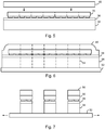
- Fig. 6 illustrates the phosphor sheet 48 which is somewhat flexible, such that it is conforming over the surface of the LED layers 30 and carrier substrate 38.
- the bottom surface of the carrier substrate 38 is affixed to a tacky stretchable sheet 52. This may be done before or after the phosphor sheet 48 is affixed to the LED layers 30.
- a suitable stretchable sheet 52 is commercially available for supporting dice during the dicing process. Support structures other than a stretchable sheet may also be used.
- the phosphor sheet 48, LED layers 30, adhesive layer 36, and carrier substrate 38 are then diced along the dashed lines 54 by any suitable technique. If the metal electrodes 34 extend to the edges of each LED, the metal electrodes 34 are also separated by the dicing process.
- the stretchable sheet 52 may be flexed over a curved surface to break the carrier substrate 38 after the carrier substrate 38 is partially sawed.
- the stretchable sheet 52 is stretched in the x and y directions to separate the LEDs by a predetermined amount.
- the phosphor layer 56 (separated from the phosphor sheet 48) is inherently aligned with the edges of the LED die 58. Therefore, the resulting light emission will be substantially uniform.
- the structure is then heated by, for example, an infrared lamp, to release the metal electrodes 34 from the adhesive layer 36, and the structure is accessed by a pick-and-place machine programmed to automatically remove each LED die 58, shown in Fig. 8 , and mount the LED die 58 on a submount wafer 60.
- a pick-and-place machine programmed to automatically remove each LED die 58, shown in Fig. 8 , and mount the LED die 58 on a submount wafer 60.
- the carrier substrate 38 is not singulated, and the sawing is only through the phosphor sheet 48 and LED layers 30.
- the adhesive layer 36 is then released from the diced LED layers 30 using UV, heat, etc.
- the pick-and-place machine can then remove each LED die individually from the carrier substrate 38. In such an embodiment, there is no need to mount the carrier substrate on the stretchable sheet 52.
- Fig. 8 shows the submount wafer 60 having top metal electrodes 62 matched to the LED's electrodes 34.
- the bonding may be by ultrasonic welding or other technique.
- the submount wafer 60 may be ceramic and have metal vias 64 that lead to bottom electrodes 66 for attachment to a printed circuit board.
- Fig. 9 is a top down view of the submount wafer 60 after being populated with an array of LED dice 58.
- a lens may be formed over each LED die 58 while on the submount wafer 60.
- Fig. 10 is a cross-sectional view of a single LED die 58 and submount 12 after dicing the submount wafer 60 and after the LED die 58 and phosphor layer 56 are encapsulated by a silicone lens 72.
- the LED can be other than a flip-chip LED and may be formed of any suitable material.
Description
- This invention relates to light emitting diodes (LEDs) with an overlying layer of phosphor to wavelength-convert the LED emission and, in particular, to a technique of laminating a phosphor layer over the LEDS.
- Prior art
Fig. 1 illustrates a conventional flip chip LED die 10 mounted on a portion of asubmount wafer 12. In a flip-chip, both the n and p contacts are formed on the same side of the LED die. - The LED die 10 is formed of semiconductor epitaxial layers, including an n-
layer 14, anactive layer 15, and a p-layer 16, grown on a growth substrate, such as a sapphire substrate. The growth substrate has been removed inFig. 1 by laser lift-off, etching, grinding, or by other techniques. In one example, the epitaxial layers are GaN based, and theactive layer 15 emits blue light. LED dies that emit UV light are also applicable to the present invention. - A
metal electrode 18 electrically contacts the p-layer 16, and ametal electrode 20 electrically contacts the n-layer 14. In one example, theelectrodes cathode metal pads submount wafer 12. Thesubmount wafer 12 hasconductive vias 24 leading tobottom metal pads submount wafer 12 and will be later singulated to form individual LEDs/submounts. - Further details of LEDs can be found in the assignee's
U.S. Patent Nos. 6,649,440 and6,274,399 , and U.S. Patent PublicationsUS 2006/0281203 A1 and2005/0269582 A1 . - While an array of
LED dies 10 are mounted on thesubmount wafer 12 or after thewafer 12 is diced, it is well known to deposit a phosphor over each LED die to generate any desired light color. To produce white light using theblue LED die 10, it is well known to deposit a YAG phosphor, or red and green phosphors, directly over thedie 10 by, for example, spraying or spin-coating the phosphor in a binder, electrophoresis, applying the phosphor in a reflective cup, or other means. It is also known to affix a preformed tile of phosphor (e.g., a sintered phosphor powder or phosphor powder in a binder) on the top of theLED die 10. Blue light leaking through the phosphor, combined with the phosphor light, produces white light. Problems with creating the phosphor layer over theLED die 10 include the difficulty in creating very uniform phosphor layer thicknesses and densities. Any variation in the thickness or density will result in color non-uniformity over the surface of the LED die. A preformed tile of phosphor may be made more uniform and allows color testing of the tile prior to affixing it to the LED die; however, it is difficult and time-consuming to precisely affix each tile (e.g., 1 mm2) to the top surface of anLED die 10. - Additionally, if a phosphor layer is deposited over all the LED dies 10 while the
LED dies 10 are mounted on thesubmount wafer 12, prior to dicing thewafer 12, much of the phosphor will be wasted since it would be deposited on portions of thewafer 12 in-between theLED dies 10. -
WO2009/126272A1 discloses a method of fabricating LEDs from a wafer comprising depositing LED epitaxial layers on a LED growth wafer. A single crystalline phosphor is bonded over at least some of the plurality of LEDs. The LED chips are then singulated from the wafer. - What is needed is a technique to create a phosphor layer over an LED die that does not suffer from the drawbacks of the prior art.
- In one embodiment of the invention, LED layers are grown over a growth substrate, such as sapphire, SiC, GaN, spinel, or other known substrate, to form an LED wafer. The type of substrate used depends on the type of LEDs to be formed. The n and p-layers are contacted by cathode and anode metal electrodes so as to create perhaps thousands of LEDs on a single substrate wafer.
- The surface of the LED wafer, prior to dicing, is adhesively fixed to a flat carrier substrate, such as by a releasable adhesive. Suitable releasable adhesives include those releasable by UV, heat, or a solvent. The LED layers are now sandwiched between the growth substrate and the carrier substrate. The carrier substrate may be a silicon wafer with an adhesive layer. Other carrier substrates include those composed of metal, glass, plastic, or any other suitable material.
- The growth substrate is then removed, while the carrier substrate provides mechanical support. In one example, the growth substrate is sapphire, the LED layers are GaN layers optionally containing A1 and In, and the sapphire substrate can be removed by laser lift-off.
- The exposed surface of the LED layers can be thinned and roughened, such as by etching or a combination of processes, to increase light extraction and remove damage caused by the laser lift-off.
- A preformed phosphor sheet approximately the size of the entire LED wafer is then affixed over the exposed surface of the LED layers. The LEDs making up the LED layers form a continuous surface since they have not been diced, so there is little waste of phosphor. The phosphor sheet may be pretested and selected to match the particular color characteristics of the LEDs on the wafer. In one embodiment, the phosphor sheet is somewhat flexible and comprises phosphor powder infused in a silicone binder. The phosphor sheet may be affixed to the LED layer surface using a thin layer of silicone.
- In one embodiment, the phosphor sheet contains a YAG phosphor (yellow-green). In another embodiment, the phosphor sheet contains mixed red and green phosphors. In another embodiment, the phosphor sheet comprises multiple layers, such as a layer of red and a separate layer of YAG to produce a warm white color. The process can be used to make any color light using any type of phosphor.
- The bottom surface of the carrier substrate may then be affixed to a tacky, stretchable sheet. Support surfaces other than a stretchable sheet may be used instead.
- The phosphor sheet, LED layers, and carrier substrate are then diced (e.g., by sawing) to separate out the LEDs. The stretchable sheet may then be pulled in the x and y directions to physically separate the LEDs by a predetermined distance. Alternately, the phosphor sheet and LED layers may be singulated on the carrier substrate (e.g., by sawing) without the carrier substrate being singulated. In such a case, the stretchable sheet is not necessary.
- The carrier substrate is then subjected to UV, heat, or a solvent to release the LED dice from the carrier substrate (whether or not the carrier substrate is diced).
- An automatic pick and place machine then removes each LED die and mounts the die to a submount wafer. The LED die metal electrodes may be bonded to the submount wafer metal electrodes by ultrasonic bonding. Further processing may be performed on the LED dies while mounted on the submount wafer, such as forming a lens over each die. The submount wafer is then diced.
- Accordingly, any phosphor waste is minimized, and it is straight forward to affix the phosphor sheet to the LED wafer. After dicing, the phosphor layer over each LED die is inherently aligned with the edges of the LED die. The phosphor layer may be uniformly thick and may have a substantially uniform density of phosphor. The resulting phosphor layer can be matched for each LED wafer so that the resulting color (e.g., white point) meets a target color. This can be important for applications where many identical LEDs are needed, such as for backlighting a large LCD television.
- The LEDs may be flip-chips, or have top and bottom electrodes, or have top electrodes only.
-
-
Fig. 1 is a cross-sectional view of a prior art blue or UV flip-chip LED die, mounted on a submount. -
Fig. 2 is a cross-sectional view of an LED wafer comprising LED layers, grown on a growth substrate, and metal electrodes formed to contact the n and p-layers at each LED location. -
Fig. 3 illustrates the structure ofFig. 2 being affixed to a carrier substrate and the growth substrate being removed using laser lift-off. -
Fig. 4 illustrates the exposed LED layer being thinned and roughened for improving light extraction. -
Fig. 5 illustrates a preformed, color-matched phosphor sheet being affixed to the LED wafer. -
Fig. 6 illustrates the carrier substrate being affixed to a tacky stretchable sheet and illustrates the dicing boundaries between the LEDs. -
Fig. 7 illustrates the LEDs after dicing and the stretchable sheet stretched in the x and y directions to separate the LEDs for a pick and place machine. The adhesive on the carrier substrate is heated to release the LEDs from the carrier substrate. -
Fig. 8 illustrates the LEDs being mounted on a submount wafer. -
Fig. 9 is a top down view of the submount wafer after being populated with an array of LEDs. Lenses may be formed over the LEDs while on the submount wafer. -
Fig. 10 is a cross-sectional view of a single LED and submount after dicing the submount wafer and after the LED and phosphor are encapsulated by a silicone lens. - Elements that are the same or equivalent are labeled with the same numeral.
-
Fig. 2 illustrates LED layers 30 grown over agrowth substrate 32. In one embodiment, the LEDs emit blue or UV light and are formed by epitaxial GaN layers, such as shown inFig. 1 . Thesubstrate 32 may be sapphire, GaN, SiC, or other suitable growth substrate. Thesubstrate 32 is typically a circular wafer.Metal electrodes 34 are formed in electrical contact with the n and p LED layers for each LED die area. Themetal electrodes 34 may be similar to theelectrodes Fig. 1 . - In another embodiment, the LEDs are not flip-chips but may have top and bottom electrodes or top electrodes only.
- The boundaries between LEDs are shown by dashed
lines 35, where the LED wafer will be later sawed or scribed and broken. - In
Fig. 3 , themetal electrodes 34 are affixed to anadhesive layer 36 on acarrier substrate 38. Thecarrier substrate 38 may be silicon since a silicon wafer can be made very flat and is relatively inexpensive. Theadhesive layer 36 is preferably a non-tacky material that softens when heated to adhere to themetal electrodes 34. Upon reheating theadhesive layer 36, themetal electrodes 34 will be released. Such adhesives are well known. Thecarrier substrate 38 should be at least as large as thegrowth substrate 32. - After the LED wafer is affixed to the
carrier substrate 38, so that there is good mechanical support for the thin LED wafer, the top surface of the GaN LED layers is exposed to pulses ofexcimer laser light 42 through thetransparent growth substrate 32. The laser light causes the surface GaN molecules to break down, and the gas released forces thegrowth substrate 32 off the LED layers 30. Thegrowth substrate 32 is then easily taken off the LED layers 30. Such a laser lift-off process is well known. - In
Fig. 4 , the exposed surface of the LED layers 30 is thinned and roughened such as byreactive ion etching 44 or other suitable process. The LED layers 30 may instead be first thinned by mechanical polishing followed by an etching process to roughen the surface to achieve a controlled degree of roughness. The thinning removes portions that have been damaged by the laser lift-off and improves light extraction. Roughening the surface reduces internal reflections and further improves light extraction. A simplified magnifiedportion 46 of the LED surface is shown inFig. 4 . - A phosphor sheet is separately formed.
Fig. 5 illustrates the preformedphosphor sheet 48. If white light is to be produced by the resulting LED, and the LED active layer emits blue light, thephosphor sheet 48 may be formed of one or more phosphors that emit red and green light when excited by blue light, and the phosphor layer must be thin enough or of sufficient low density to allow some blue light to pass through and combine with the red and green components. Suitable phosphors include a YAG phosphor (produces yellow-green light), combinations of red and green phosphors, or a combination of a YAG phosphor with a red phosphor to produce a warmer white light. If the LED generates UV light, a blue phosphor may also be included in thephosphor sheet 48. - In one embodiment, to create the
phosphor sheet 48, the phosphor powder is mixed with silicone to achieve a target phosphor density, and thephosphor sheet 48 is formed to have a target thickness. The desired thickness may be obtaining by spinning the mixture on a flat surface or molding the phosphor sheet. Alternatively, thephosphor sheet 48 may be sawed from an elongated boule of phosphor to the desired thickness. - After the
phosphor sheet 48 is formed, thephosphor sheet 48 may be tested by energizing thephosphor sheet 48 using a blue light source and measuring the light emission. Since blue LEDs in different wafers generally emit slightly different dominant wavelengths, the blue LEDs may be tested while part of the LED wafer. Preformed phosphor sheets of varying thicknesses or phosphor densities are then matched up with particular LED wafers so that the resulting color emissions may all have the same target white point (or CCT). Producing LEDs that output substantially identical white points is particularly valuable for applications that require matched LEDs such as for backlighting a large LCD television. - In one embodiment, the
phosphor sheet 48 is on the order of a few hundred microns thick and somewhat flexible. Thephosphor sheet 48 is preferably the same size as the LED wafer or larger. - As shown in
Fig. 5 , the matchedphosphor sheet 48 is placed over the LED layers 30, and a vacuum can be drawn between thephosphor sheet 48 and the LED layers 30 to remove all air. Thephosphor sheet 48 can then be laminated to the LED layers 30 using heat and pressure (assuming there is sufficient silicone in the phosphor sheet 48). This will conform thephosphor sheet 48 to the top surface of the LED layers 30. For aphosphor sheet 48 not containing an appropriate type of silicone or for asintered phosphor sheet 48, a thin layer of silicone is applied over the LED layers 30 orphosphor sheet 48 to act as an adhesive for laminating thephosphor sheet 48 to the LED layers 30 using pressure. The silicone may be cured by heat or UV. - By laminating a preformed phosphor sheet onto the
LED layer 30 prior to the LEDs being diced, at least the following advantages result: 1) there is little wasted phosphor since almost all the phosphor coats an LED; 2) the phosphor over each LED may have a uniform thickness and density; 3) it is fairly easy to properly position the phosphor sheet over the LED wafer and affix it to the LED wafer; 4) the phosphor sheet may be color-matched to the particular LED color emission; 5) when the LEDs are diced, the phosphor layer will precisely align with the edges of the LED to produce uniform color; and 6) the phosphor sheet may be formed of multiple layers, each layer being customized and precisely formed. In one embodiment, a multi-layer phosphor sheet is preformed by lamination, and the sheet is tested and then laminated as a single sheet to the LED layers 30. Alternatively, the multiple layers may be individually laminated over the LED layers 30. The multiple layers may be a YAG layer and a red phosphor layer. -
Fig. 6 illustrates thephosphor sheet 48 which is somewhat flexible, such that it is conforming over the surface of the LED layers 30 andcarrier substrate 38. InFig. 6 , the bottom surface of thecarrier substrate 38 is affixed to a tackystretchable sheet 52. This may be done before or after thephosphor sheet 48 is affixed to the LED layers 30. A suitablestretchable sheet 52 is commercially available for supporting dice during the dicing process. Support structures other than a stretchable sheet may also be used. - The
phosphor sheet 48, LED layers 30,adhesive layer 36, andcarrier substrate 38 are then diced along the dashedlines 54 by any suitable technique. If themetal electrodes 34 extend to the edges of each LED, themetal electrodes 34 are also separated by the dicing process. Thestretchable sheet 52 may be flexed over a curved surface to break thecarrier substrate 38 after thecarrier substrate 38 is partially sawed. - As shown in
Fig. 7 , thestretchable sheet 52 is stretched in the x and y directions to separate the LEDs by a predetermined amount. Note that the phosphor layer 56 (separated from the phosphor sheet 48) is inherently aligned with the edges of the LED die 58. Therefore, the resulting light emission will be substantially uniform. - The structure is then heated by, for example, an infrared lamp, to release the
metal electrodes 34 from theadhesive layer 36, and the structure is accessed by a pick-and-place machine programmed to automatically remove each LED die 58, shown inFig. 8 , and mount the LED die 58 on asubmount wafer 60. - In another embodiment, the
carrier substrate 38 is not singulated, and the sawing is only through thephosphor sheet 48 and LED layers 30. Theadhesive layer 36 is then released from the diced LED layers 30 using UV, heat, etc. The pick-and-place machine can then remove each LED die individually from thecarrier substrate 38. In such an embodiment, there is no need to mount the carrier substrate on thestretchable sheet 52. -
Fig. 8 shows thesubmount wafer 60 havingtop metal electrodes 62 matched to the LED'selectrodes 34. The bonding may be by ultrasonic welding or other technique. Thesubmount wafer 60 may be ceramic and havemetal vias 64 that lead tobottom electrodes 66 for attachment to a printed circuit board. -
Fig. 9 is a top down view of thesubmount wafer 60 after being populated with an array ofLED dice 58. A lens may be formed over each LED die 58 while on thesubmount wafer 60. -
Fig. 10 is a cross-sectional view of a single LED die 58 andsubmount 12 after dicing thesubmount wafer 60 and after the LED die 58 andphosphor layer 56 are encapsulated by asilicone lens 72. The LED can be other than a flip-chip LED and may be formed of any suitable material.
Claims (13)
- A method for fabricating a light emitting diode (LED) device comprising:growing LED layers (30) on a growth substrate (32);providing a preformed flexible phosphor sheet (48) separate from the LED layers (30);affixing the LED layers (30) to a carrier substrate (38) using a releasable adhesive;removing the growth substrate (32) while the carrier substrate (38) provides mechanical support for the LED layers (30);laminating the preformed flexible phosphor sheet (48) to an exposed surface of the LED layers (30), such that the flexible phosphor sheet is conforming over the surface of the LED layers; dicing the phosphor sheet (48), the LED layers (30) and the carrier substrate (38) to create separate LED dice, each having an overlying phosphor layer;releasing the LED layers (30) from the releasable adhesive; andremoving the LED dice from the carrier substrate (38).
- The method of Claim 1 wherein the LED layers (30) comprise an n-layer and a p-layer, the method further comprising forming metal electrodes (34) contacting the n-layer and the p-layer prior to affixing the LED layers (30) to the carrier substrate (38).
- The method of Claim 2 wherein affixing the LED layers (30) to the carrier substrate (38) comprises affixing at least some of the metal electrodes (34) to the carrier substrate (38).
- The method of Claim 1 wherein the LED layers (30) emit blue light when energized, and the phosphor sheet (48) emits red light wavelengths and green light wavelengths when energized by the blue light, such that the LED dice emit white light when the LED dice are energized.
- The method of Claim 4 wherein the phosphor sheet (48) comprises a YAG phosphor.
- The method of Claim 1 wherein the phosphor sheet (48) has an area approximately the same as or larger than an area of the growth substrate (32).
- The method of Claim 1 wherein the phosphor sheet (48) has a substantially uniform thickness.
- The method of Claim 1 further comprising mounting the carrier substrate (38) on an adhesive sheet, and wherein dicing the phosphor sheet (48) and the LED layers (30) comprises also dicing the carrier substrate (38) but not the adhesive sheet.
- The method of Claim 1 wherein removing the growth substrate (32) comprises removing the growth substrate using a laser lift-off process.
- The method of Claim 1 wherein the releasable adhesive comprises an adhesive releasable by at least one of UV light, heat, or a solvent.
- The method of Claim 1 further comprising mounting the LED dice on a submount wafer by bonding electrodes on the submount wafer to corresponding electrodes of the LED dice.
- The method of Claim 1 further comprising using a pick-and-place machine to remove the LED dice individually from the carrier substrate (38).
- The method of Claim 1 wherein the step of laminating the flexible phosphor sheet (48) comprises using heat and pressure such that the flexible phosphor sheet conforms to the exposed surface of the LED layers (30).
Applications Claiming Priority (2)
| Application Number | Priority Date | Filing Date | Title |
|---|---|---|---|
| US12/771,809 US8232117B2 (en) | 2010-04-30 | 2010-04-30 | LED wafer with laminated phosphor layer |
| PCT/IB2011/051849 WO2011135528A1 (en) | 2010-04-30 | 2011-04-27 | Led wafer with laminated phosphor layer |
Publications (2)
| Publication Number | Publication Date |
|---|---|
| EP2564435A1 EP2564435A1 (en) | 2013-03-06 |
| EP2564435B1 true EP2564435B1 (en) | 2017-09-27 |
Family
ID=44120320
Family Applications (1)
| Application Number | Title | Priority Date | Filing Date |
|---|---|---|---|
| EP11722561.5A Active EP2564435B1 (en) | 2010-04-30 | 2011-04-27 | Method for fabricating a light emitting diode with a laminated phosphor layer |
Country Status (7)
| Country | Link |
|---|---|
| US (1) | US8232117B2 (en) |
| EP (1) | EP2564435B1 (en) |
| JP (1) | JP5927179B2 (en) |
| KR (1) | KR101813099B1 (en) |
| CN (1) | CN102906887B (en) |
| TW (1) | TWI538245B (en) |
| WO (1) | WO2011135528A1 (en) |
Families Citing this family (49)
| Publication number | Priority date | Publication date | Assignee | Title |
|---|---|---|---|---|
| US20110284866A1 (en) * | 2005-01-11 | 2011-11-24 | Tran Chuong A | Light-emitting diode (led) structure having a wavelength-converting layer and method of producing |
| US9263314B2 (en) | 2010-08-06 | 2016-02-16 | Brewer Science Inc. | Multiple bonding layers for thin-wafer handling |
| KR20120061376A (en) * | 2010-12-03 | 2012-06-13 | 삼성엘이디 주식회사 | Method of applying phosphor on semiconductor light emitting device |
| KR101725220B1 (en) * | 2010-12-22 | 2017-04-10 | 삼성전자 주식회사 | Method of depositing phosphor on semiconductor light emitting device and an apparatus for depositing phosphor on semiconductor light emitting device |
| DE102011013369A1 (en) * | 2010-12-30 | 2012-07-05 | Osram Opto Semiconductors Gmbh | A method of manufacturing a plurality of semiconductor devices |
| JP5670249B2 (en) * | 2011-04-14 | 2015-02-18 | 日東電工株式会社 | Light emitting element transfer sheet manufacturing method, light emitting device manufacturing method, light emitting element transfer sheet, and light emitting device |
| US9653643B2 (en) * | 2012-04-09 | 2017-05-16 | Cree, Inc. | Wafer level packaging of light emitting diodes (LEDs) |
| US9666764B2 (en) | 2012-04-09 | 2017-05-30 | Cree, Inc. | Wafer level packaging of multiple light emitting diodes (LEDs) on a single carrier die |
| JP6013685B2 (en) | 2011-07-22 | 2016-10-25 | 株式会社半導体エネルギー研究所 | Semiconductor device |
| US9035344B2 (en) * | 2011-09-14 | 2015-05-19 | VerLASE TECHNOLOGIES LLC | Phosphors for use with LEDs and other optoelectronic devices |
| KR101817807B1 (en) | 2011-09-20 | 2018-01-11 | 엘지이노텍 주식회사 | Light emitting device package and lighting system including the same |
| DE102012101211A1 (en) * | 2012-02-15 | 2013-08-22 | Osram Opto Semiconductors Gmbh | Method for producing a radiation-emitting semiconductor component |
| CN104205365B (en) * | 2012-03-19 | 2020-06-16 | 亮锐控股有限公司 | Singulation of light emitting devices before and after phosphor application |
| WO2013144919A1 (en) | 2012-03-29 | 2013-10-03 | Koninklijke Philips N.V. | Phosphor in inorganic binder for led applications |
| WO2013144777A1 (en) | 2012-03-29 | 2013-10-03 | Koninklijke Philips N.V. | Phosphor in inorganic binder for led applications |
| US9847445B2 (en) * | 2012-04-05 | 2017-12-19 | Koninklijke Philips N.V. | LED thin-film device partial singulation prior to substrate thinning or removal |
| US9608016B2 (en) * | 2012-05-17 | 2017-03-28 | Koninklijke Philips N.V. | Method of separating a wafer of semiconductor devices |
| US20140001949A1 (en) * | 2012-06-29 | 2014-01-02 | Nitto Denko Corporation | Phosphor layer-covered led, producing method thereof, and led device |
| US20140009060A1 (en) * | 2012-06-29 | 2014-01-09 | Nitto Denko Corporation | Phosphor layer-covered led, producing method thereof, and led device |
| US20140001948A1 (en) * | 2012-06-29 | 2014-01-02 | Nitto Denko Corporation | Reflecting layer-phosphor layer-covered led, producing method thereof, led device, and producing method thereof |
| US8876312B2 (en) | 2013-03-05 | 2014-11-04 | Avago Technologies General Ip (Singapore) Pte. Ltd. | Lighting device and apparatus with spectral converter within a casing |
| US8928219B2 (en) | 2013-03-05 | 2015-01-06 | Avago Technologies General Ip (Singapore) Pte. Ltd. | Lighting device with spectral converter |
| DE102013212247B4 (en) * | 2013-06-26 | 2021-10-21 | OSRAM Opto Semiconductors Gesellschaft mit beschränkter Haftung | Optoelectronic component and process for its production |
| EP3118903B1 (en) * | 2013-07-18 | 2023-06-21 | Lumileds LLC | Dicing a wafer of light emitting devices |
| KR102299238B1 (en) * | 2014-01-08 | 2021-09-07 | 루미리즈 홀딩 비.브이. | Wavelength converted semiconductor light emitting device |
| KR102145208B1 (en) | 2014-06-10 | 2020-08-19 | 삼성전자주식회사 | Manufacturing method of light emitting device package |
| EP3158594A1 (en) * | 2014-06-19 | 2017-04-26 | Koninklijke Philips N.V. | Wavelength converted light emitting device with small source size |
| KR102345751B1 (en) | 2015-01-05 | 2022-01-03 | 삼성전자주식회사 | Semiconductor light emitting device package and method for manufacturing the same |
| JP6806774B2 (en) | 2015-12-07 | 2021-01-06 | グロ アーベーGlo Ab | Laser lift-off on isolated group III nitride optical islands for inter-board LED transfer |
| JP2017157593A (en) | 2016-02-29 | 2017-09-07 | 三星電子株式会社Samsung Electronics Co.,Ltd. | Light-emitting diode, manufacturing method for light-emitting diode, light-emitting diode display device, and manufacturing method for light-emitting diode display device |
| US10193031B2 (en) | 2016-03-11 | 2019-01-29 | Rohinni, LLC | Method for applying phosphor to light emitting diodes and apparatus thereof |
| DE102016108682A1 (en) | 2016-05-11 | 2017-11-16 | Osram Opto Semiconductors Gmbh | Method for producing an optoelectronic component and optoelectronic component |
| CN106876528A (en) * | 2016-12-30 | 2017-06-20 | 东莞中之光电股份有限公司 | LED packaging manufacturing process |
| CN106876551A (en) * | 2016-12-30 | 2017-06-20 | 东莞中之光电股份有限公司 | Chip-scale LED packaging technologies |
| WO2018154868A1 (en) * | 2017-02-27 | 2018-08-30 | パナソニックIpマネジメント株式会社 | Wavelength conversion member |
| US10686158B2 (en) * | 2017-03-31 | 2020-06-16 | Innolux Corporation | Display device |
| US10964851B2 (en) * | 2017-08-30 | 2021-03-30 | SemiLEDs Optoelectronics Co., Ltd. | Single light emitting diode (LED) structure |
| US11335835B2 (en) | 2017-12-20 | 2022-05-17 | Lumileds Llc | Converter fill for LED array |
| US11527482B2 (en) | 2017-12-22 | 2022-12-13 | Hrl Laboratories, Llc | Hybrid integrated circuit architecture |
| US11536800B2 (en) | 2017-12-22 | 2022-12-27 | Hrl Laboratories, Llc | Method and apparatus to increase radar range |
| WO2019125587A1 (en) | 2017-12-22 | 2019-06-27 | Hrl Laboratories, Llc | Hybrid integrated circuit architecture |
| US10957537B2 (en) * | 2018-11-12 | 2021-03-23 | Hrl Laboratories, Llc | Methods to design and uniformly co-fabricate small vias and large cavities through a substrate |
| US10910433B2 (en) | 2018-12-31 | 2021-02-02 | Lumileds Llc | Pixelated LED array with optical elements |
| KR102346212B1 (en) | 2018-12-31 | 2022-01-03 | 주식회사 나노엑스 | Led chips for emitting doubleside |
| EP4002469A4 (en) * | 2019-07-19 | 2023-04-05 | Lg Electronics Inc. | Display device using micro led, and manufacturing method therefor |
| US11527684B2 (en) | 2020-12-04 | 2022-12-13 | Lumileds Llc | Patterned downconverter and adhesive film for micro-LED, mini-LED downconverter mass transfer |
| CN113611786B (en) * | 2021-08-02 | 2022-09-27 | 东莞市中麒光电技术有限公司 | LED chip bulk transfer method with high peeling yield and convenient film pouring |
| CN113764550B (en) * | 2021-09-07 | 2023-01-24 | 东莞市中麒光电技术有限公司 | Transfer method for preventing LED chip from being damaged |
| CN113764551B (en) * | 2021-09-07 | 2023-01-03 | 东莞市中麒光电技术有限公司 | LED chip transfer method |
Family Cites Families (28)
| Publication number | Priority date | Publication date | Assignee | Title |
|---|---|---|---|---|
| US6194742B1 (en) | 1998-06-05 | 2001-02-27 | Lumileds Lighting, U.S., Llc | Strain engineered and impurity controlled III-V nitride semiconductor films and optoelectronic devices |
| US6133589A (en) | 1999-06-08 | 2000-10-17 | Lumileds Lighting, U.S., Llc | AlGaInN-based LED having thick epitaxial layer for improved light extraction |
| JP3747807B2 (en) * | 2001-06-12 | 2006-02-22 | ソニー株式会社 | Device mounting substrate and defective device repair method |
| US6693041B2 (en) * | 2001-06-20 | 2004-02-17 | International Business Machines Corporation | Self-aligned STI for narrow trenches |
| CN1323441C (en) * | 2001-10-12 | 2007-06-27 | 日亚化学工业株式会社 | Light-emitting device and its mfg. method |
| US20060003477A1 (en) * | 2002-10-30 | 2006-01-05 | Bert Braune | Method for producing a light source provided with electroluminescent diodes and comprising a luminescence conversion element |
| TWI246783B (en) | 2003-09-24 | 2006-01-01 | Matsushita Electric Works Ltd | Light-emitting device and its manufacturing method |
| US7008861B2 (en) * | 2003-12-11 | 2006-03-07 | Cree, Inc. | Semiconductor substrate assemblies and methods for preparing and dicing the same |
| JP4496774B2 (en) | 2003-12-22 | 2010-07-07 | 日亜化学工業株式会社 | Manufacturing method of semiconductor device |
| US7259030B2 (en) * | 2004-03-29 | 2007-08-21 | Articulated Technologies, Llc | Roll-to-roll fabricated light sheet and encapsulated semiconductor circuit devices |
| US7361938B2 (en) | 2004-06-03 | 2008-04-22 | Philips Lumileds Lighting Company Llc | Luminescent ceramic for a light emitting device |
| US7754507B2 (en) | 2005-06-09 | 2010-07-13 | Philips Lumileds Lighting Company, Llc | Method of removing the growth substrate of a semiconductor light emitting device |
| US7344952B2 (en) * | 2005-10-28 | 2008-03-18 | Philips Lumileds Lighting Company, Llc | Laminating encapsulant film containing phosphor over LEDs |
| US7968379B2 (en) | 2006-03-09 | 2011-06-28 | SemiLEDs Optoelectronics Co., Ltd. | Method of separating semiconductor dies |
| US7452739B2 (en) * | 2006-03-09 | 2008-11-18 | Semi-Photonics Co., Ltd. | Method of separating semiconductor dies |
| TWI420691B (en) * | 2006-11-20 | 2013-12-21 | 尼康股份有限公司 | Led device and the fabricating method thereof |
| US9024349B2 (en) | 2007-01-22 | 2015-05-05 | Cree, Inc. | Wafer level phosphor coating method and devices fabricated utilizing method |
| US20080225549A1 (en) * | 2007-02-26 | 2008-09-18 | Mahendra Dassanayake | Linear Optic Light Coupler |
| JP5186800B2 (en) * | 2007-04-28 | 2013-04-24 | 日亜化学工業株式会社 | Nitride semiconductor light emitting device, light emitting device including the same, and method for manufacturing nitride semiconductor light emitting device |
| JP5158472B2 (en) * | 2007-05-24 | 2013-03-06 | スタンレー電気株式会社 | Semiconductor light emitting device |
| US20090053869A1 (en) * | 2007-08-22 | 2009-02-26 | Infineon Technologies Austria Ag | Method for producing an integrated circuit including a trench transistor and integrated circuit |
| US20090140279A1 (en) * | 2007-12-03 | 2009-06-04 | Goldeneye, Inc. | Substrate-free light emitting diode chip |
| US20090173958A1 (en) | 2008-01-04 | 2009-07-09 | Cree, Inc. | Light emitting devices with high efficiency phospor structures |
| US8878219B2 (en) | 2008-01-11 | 2014-11-04 | Cree, Inc. | Flip-chip phosphor coating method and devices fabricated utilizing method |
| US7859000B2 (en) | 2008-04-10 | 2010-12-28 | Cree, Inc. | LEDs using single crystalline phosphor and methods of fabricating same |
| US8193565B2 (en) * | 2008-04-18 | 2012-06-05 | Fairchild Semiconductor Corporation | Multi-level lateral floating coupled capacitor transistor structures |
| US10147843B2 (en) | 2008-07-24 | 2018-12-04 | Lumileds Llc | Semiconductor light emitting device including a window layer and a light-directing structure |
| US7973327B2 (en) * | 2008-09-02 | 2011-07-05 | Bridgelux, Inc. | Phosphor-converted LED |
-
2010
- 2010-04-30 US US12/771,809 patent/US8232117B2/en active Active
-
2011
- 2011-04-22 TW TW100114123A patent/TWI538245B/en active
- 2011-04-27 JP JP2013506794A patent/JP5927179B2/en active Active
- 2011-04-27 EP EP11722561.5A patent/EP2564435B1/en active Active
- 2011-04-27 CN CN201180021821.8A patent/CN102906887B/en active Active
- 2011-04-27 KR KR1020127031301A patent/KR101813099B1/en active IP Right Grant
- 2011-04-27 WO PCT/IB2011/051849 patent/WO2011135528A1/en active Application Filing
Non-Patent Citations (1)
| Title |
|---|
| None * |
Also Published As
| Publication number | Publication date |
|---|---|
| CN102906887B (en) | 2016-05-11 |
| KR20130095190A (en) | 2013-08-27 |
| US20110266569A1 (en) | 2011-11-03 |
| KR101813099B1 (en) | 2017-12-29 |
| WO2011135528A1 (en) | 2011-11-03 |
| CN102906887A (en) | 2013-01-30 |
| US8232117B2 (en) | 2012-07-31 |
| TW201203596A (en) | 2012-01-16 |
| TWI538245B (en) | 2016-06-11 |
| JP5927179B2 (en) | 2016-06-01 |
| JP2013526052A (en) | 2013-06-20 |
| EP2564435A1 (en) | 2013-03-06 |
Similar Documents
| Publication | Publication Date | Title |
|---|---|---|
| EP2564435B1 (en) | Method for fabricating a light emitting diode with a laminated phosphor layer | |
| EP2206165B1 (en) | Robust light emitting diode structure with removed substrate and added optical element, method of manufacturing the same | |
| TWI521746B (en) | Light emitting device and method of manufacturing the light emitting device | |
| TWI476944B (en) | Single crystal phosphor light conversion structures for light emitting devices | |
| US20110049545A1 (en) | Led package with phosphor plate and reflective substrate | |
| US20110031516A1 (en) | Led with silicone layer and laminated remote phosphor layer | |
| JP2018014509A (en) | LED structure | |
| EP1690300A2 (en) | Semiconductor light emitting device, lighting module, lighting apparatus, and manufacturing method of semiconductor light emitting device | |
| EP2870641B1 (en) | Phosphor separated from led by transparent spacer | |
| TW201142993A (en) | Light emitting diode wafer-level package with self-aligning features | |
| TW201216526A (en) | Lamination process for LEDs | |
| US8921130B2 (en) | Methods for producing and placing wavelength converting structures | |
| WO2014094363A1 (en) | Method for preparing gan-based white-light flip chip | |
| WO2013175338A1 (en) | Phosphor coating process for discrete light emitting devices | |
| WO2015077612A1 (en) | Method of stress induced cleaving of semiconductor devices | |
| TWI740212B (en) | Method for manufacturing micro-led chip | |
| JP2003069085A (en) | Multilayered wiring structure or electrode lead-out structure, electric circuit device, and their manufacturing methods | |
| JP2013004528A (en) | Semiconductor device and manufacturing method of the same |
Legal Events
| Date | Code | Title | Description |
|---|---|---|---|
| PUAI | Public reference made under article 153(3) epc to a published international application that has entered the european phase |
Free format text: ORIGINAL CODE: 0009012 |
|
| 17P | Request for examination filed |
Effective date: 20121130 |
|
| AK | Designated contracting states |
Kind code of ref document: A1 Designated state(s): AL AT BE BG CH CY CZ DE DK EE ES FI FR GB GR HR HU IE IS IT LI LT LU LV MC MK MT NL NO PL PT RO RS SE SI SK SM TR |
|
| DAX | Request for extension of the european patent (deleted) | ||
| RAP1 | Party data changed (applicant data changed or rights of an application transferred) |
Owner name: PHILIPS LUMILEDS LIGHTING COMPANY, LLC Owner name: KONINKLIJKE PHILIPS N.V. |
|
| REG | Reference to a national code |
Ref country code: DE Ref legal event code: R079 Ref document number: 602011041890 Country of ref document: DE Free format text: PREVIOUS MAIN CLASS: H01L0033000000 Ipc: H01L0023000000 |
|
| GRAP | Despatch of communication of intention to grant a patent |
Free format text: ORIGINAL CODE: EPIDOSNIGR1 |
|
| RIC1 | Information provided on ipc code assigned before grant |
Ipc: H01L 23/00 20060101AFI20170629BHEP Ipc: H01L 33/00 20100101ALI20170629BHEP Ipc: H01L 33/50 20100101ALI20170629BHEP Ipc: H01L 33/22 20100101ALN20170629BHEP |
|
| RIC1 | Information provided on ipc code assigned before grant |
Ipc: H01L 33/00 20100101ALI20170705BHEP Ipc: H01L 33/50 20100101ALI20170705BHEP Ipc: H01L 23/00 20060101AFI20170705BHEP Ipc: H01L 33/22 20100101ALN20170705BHEP |
|
| INTG | Intention to grant announced |
Effective date: 20170717 |
|
| GRAS | Grant fee paid |
Free format text: ORIGINAL CODE: EPIDOSNIGR3 |
|
| GRAA | (expected) grant |
Free format text: ORIGINAL CODE: 0009210 |
|
| AK | Designated contracting states |
Kind code of ref document: B1 Designated state(s): AL AT BE BG CH CY CZ DE DK EE ES FI FR GB GR HR HU IE IS IT LI LT LU LV MC MK MT NL NO PL PT RO RS SE SI SK SM TR |
|
| REG | Reference to a national code |
Ref country code: GB Ref legal event code: FG4D |
|
| REG | Reference to a national code |
Ref country code: CH Ref legal event code: EP |
|
| REG | Reference to a national code |
Ref country code: AT Ref legal event code: REF Ref document number: 932730 Country of ref document: AT Kind code of ref document: T Effective date: 20171015 |
|
| REG | Reference to a national code |
Ref country code: IE Ref legal event code: FG4D |
|
| REG | Reference to a national code |
Ref country code: DE Ref legal event code: R096 Ref document number: 602011041890 Country of ref document: DE |
|
| PG25 | Lapsed in a contracting state [announced via postgrant information from national office to epo] |
Ref country code: HR Free format text: LAPSE BECAUSE OF FAILURE TO SUBMIT A TRANSLATION OF THE DESCRIPTION OR TO PAY THE FEE WITHIN THE PRESCRIBED TIME-LIMIT Effective date: 20170927 Ref country code: SE Free format text: LAPSE BECAUSE OF FAILURE TO SUBMIT A TRANSLATION OF THE DESCRIPTION OR TO PAY THE FEE WITHIN THE PRESCRIBED TIME-LIMIT Effective date: 20170927 Ref country code: NO Free format text: LAPSE BECAUSE OF FAILURE TO SUBMIT A TRANSLATION OF THE DESCRIPTION OR TO PAY THE FEE WITHIN THE PRESCRIBED TIME-LIMIT Effective date: 20171227 Ref country code: FI Free format text: LAPSE BECAUSE OF FAILURE TO SUBMIT A TRANSLATION OF THE DESCRIPTION OR TO PAY THE FEE WITHIN THE PRESCRIBED TIME-LIMIT Effective date: 20170927 Ref country code: LT Free format text: LAPSE BECAUSE OF FAILURE TO SUBMIT A TRANSLATION OF THE DESCRIPTION OR TO PAY THE FEE WITHIN THE PRESCRIBED TIME-LIMIT Effective date: 20170927 |
|
| REG | Reference to a national code |
Ref country code: NL Ref legal event code: MP Effective date: 20170927 |
|
| REG | Reference to a national code |
Ref country code: LT Ref legal event code: MG4D |
|
| REG | Reference to a national code |
Ref country code: AT Ref legal event code: MK05 Ref document number: 932730 Country of ref document: AT Kind code of ref document: T Effective date: 20170927 |
|
| PG25 | Lapsed in a contracting state [announced via postgrant information from national office to epo] |
Ref country code: BG Free format text: LAPSE BECAUSE OF FAILURE TO SUBMIT A TRANSLATION OF THE DESCRIPTION OR TO PAY THE FEE WITHIN THE PRESCRIBED TIME-LIMIT Effective date: 20171227 Ref country code: GR Free format text: LAPSE BECAUSE OF FAILURE TO SUBMIT A TRANSLATION OF THE DESCRIPTION OR TO PAY THE FEE WITHIN THE PRESCRIBED TIME-LIMIT Effective date: 20171228 Ref country code: RS Free format text: LAPSE BECAUSE OF FAILURE TO SUBMIT A TRANSLATION OF THE DESCRIPTION OR TO PAY THE FEE WITHIN THE PRESCRIBED TIME-LIMIT Effective date: 20170927 Ref country code: LV Free format text: LAPSE BECAUSE OF FAILURE TO SUBMIT A TRANSLATION OF THE DESCRIPTION OR TO PAY THE FEE WITHIN THE PRESCRIBED TIME-LIMIT Effective date: 20170927 |
|
| RAP2 | Party data changed (patent owner data changed or rights of a patent transferred) |
Owner name: LUMILEDS HOLDING B.V. |
|
| PG25 | Lapsed in a contracting state [announced via postgrant information from national office to epo] |
Ref country code: NL Free format text: LAPSE BECAUSE OF FAILURE TO SUBMIT A TRANSLATION OF THE DESCRIPTION OR TO PAY THE FEE WITHIN THE PRESCRIBED TIME-LIMIT Effective date: 20170927 |
|
| REG | Reference to a national code |
Ref country code: FR Ref legal event code: PLFP Year of fee payment: 8 |
|
| PG25 | Lapsed in a contracting state [announced via postgrant information from national office to epo] |
Ref country code: RO Free format text: LAPSE BECAUSE OF FAILURE TO SUBMIT A TRANSLATION OF THE DESCRIPTION OR TO PAY THE FEE WITHIN THE PRESCRIBED TIME-LIMIT Effective date: 20170927 Ref country code: ES Free format text: LAPSE BECAUSE OF FAILURE TO SUBMIT A TRANSLATION OF THE DESCRIPTION OR TO PAY THE FEE WITHIN THE PRESCRIBED TIME-LIMIT Effective date: 20170927 Ref country code: CZ Free format text: LAPSE BECAUSE OF FAILURE TO SUBMIT A TRANSLATION OF THE DESCRIPTION OR TO PAY THE FEE WITHIN THE PRESCRIBED TIME-LIMIT Effective date: 20170927 |
|
| PG25 | Lapsed in a contracting state [announced via postgrant information from national office to epo] |
Ref country code: SK Free format text: LAPSE BECAUSE OF FAILURE TO SUBMIT A TRANSLATION OF THE DESCRIPTION OR TO PAY THE FEE WITHIN THE PRESCRIBED TIME-LIMIT Effective date: 20170927 Ref country code: IS Free format text: LAPSE BECAUSE OF FAILURE TO SUBMIT A TRANSLATION OF THE DESCRIPTION OR TO PAY THE FEE WITHIN THE PRESCRIBED TIME-LIMIT Effective date: 20180127 Ref country code: IT Free format text: LAPSE BECAUSE OF FAILURE TO SUBMIT A TRANSLATION OF THE DESCRIPTION OR TO PAY THE FEE WITHIN THE PRESCRIBED TIME-LIMIT Effective date: 20170927 Ref country code: EE Free format text: LAPSE BECAUSE OF FAILURE TO SUBMIT A TRANSLATION OF THE DESCRIPTION OR TO PAY THE FEE WITHIN THE PRESCRIBED TIME-LIMIT Effective date: 20170927 Ref country code: SM Free format text: LAPSE BECAUSE OF FAILURE TO SUBMIT A TRANSLATION OF THE DESCRIPTION OR TO PAY THE FEE WITHIN THE PRESCRIBED TIME-LIMIT Effective date: 20170927 Ref country code: AT Free format text: LAPSE BECAUSE OF FAILURE TO SUBMIT A TRANSLATION OF THE DESCRIPTION OR TO PAY THE FEE WITHIN THE PRESCRIBED TIME-LIMIT Effective date: 20170927 |
|
| REG | Reference to a national code |
Ref country code: DE Ref legal event code: R097 Ref document number: 602011041890 Country of ref document: DE |
|
| REG | Reference to a national code |
Ref country code: FR Ref legal event code: CD Owner name: LUMILEDS HOLDING B.V., NL Effective date: 20180611 |
|
| PG25 | Lapsed in a contracting state [announced via postgrant information from national office to epo] |
Ref country code: DK Free format text: LAPSE BECAUSE OF FAILURE TO SUBMIT A TRANSLATION OF THE DESCRIPTION OR TO PAY THE FEE WITHIN THE PRESCRIBED TIME-LIMIT Effective date: 20170927 |
|
| PLBE | No opposition filed within time limit |
Free format text: ORIGINAL CODE: 0009261 |
|
| STAA | Information on the status of an ep patent application or granted ep patent |
Free format text: STATUS: NO OPPOSITION FILED WITHIN TIME LIMIT |
|
| PG25 | Lapsed in a contracting state [announced via postgrant information from national office to epo] |
Ref country code: PL Free format text: LAPSE BECAUSE OF FAILURE TO SUBMIT A TRANSLATION OF THE DESCRIPTION OR TO PAY THE FEE WITHIN THE PRESCRIBED TIME-LIMIT Effective date: 20170927 |
|
| 26N | No opposition filed |
Effective date: 20180628 |
|
| PG25 | Lapsed in a contracting state [announced via postgrant information from national office to epo] |
Ref country code: SI Free format text: LAPSE BECAUSE OF FAILURE TO SUBMIT A TRANSLATION OF THE DESCRIPTION OR TO PAY THE FEE WITHIN THE PRESCRIBED TIME-LIMIT Effective date: 20170927 Ref country code: MC Free format text: LAPSE BECAUSE OF FAILURE TO SUBMIT A TRANSLATION OF THE DESCRIPTION OR TO PAY THE FEE WITHIN THE PRESCRIBED TIME-LIMIT Effective date: 20170927 |
|
| REG | Reference to a national code |
Ref country code: FR Ref legal event code: CA Effective date: 20181026 Ref country code: CH Ref legal event code: PL Ref country code: FR Ref legal event code: TP Owner name: LUMILEDS HOLDING B.V., NL Effective date: 20181026 |
|
| REG | Reference to a national code |
Ref country code: BE Ref legal event code: MM Effective date: 20180430 |
|
| REG | Reference to a national code |
Ref country code: IE Ref legal event code: MM4A |
|
| PG25 | Lapsed in a contracting state [announced via postgrant information from national office to epo] |
Ref country code: LU Free format text: LAPSE BECAUSE OF NON-PAYMENT OF DUE FEES Effective date: 20180427 |
|
| PG25 | Lapsed in a contracting state [announced via postgrant information from national office to epo] |
Ref country code: BE Free format text: LAPSE BECAUSE OF NON-PAYMENT OF DUE FEES Effective date: 20180430 Ref country code: CH Free format text: LAPSE BECAUSE OF NON-PAYMENT OF DUE FEES Effective date: 20180430 Ref country code: LI Free format text: LAPSE BECAUSE OF NON-PAYMENT OF DUE FEES Effective date: 20180430 |
|
| PG25 | Lapsed in a contracting state [announced via postgrant information from national office to epo] |
Ref country code: IE Free format text: LAPSE BECAUSE OF NON-PAYMENT OF DUE FEES Effective date: 20180427 |
|
| PG25 | Lapsed in a contracting state [announced via postgrant information from national office to epo] |
Ref country code: MT Free format text: LAPSE BECAUSE OF NON-PAYMENT OF DUE FEES Effective date: 20180427 |
|
| PG25 | Lapsed in a contracting state [announced via postgrant information from national office to epo] |
Ref country code: TR Free format text: LAPSE BECAUSE OF FAILURE TO SUBMIT A TRANSLATION OF THE DESCRIPTION OR TO PAY THE FEE WITHIN THE PRESCRIBED TIME-LIMIT Effective date: 20170927 |
|
| PG25 | Lapsed in a contracting state [announced via postgrant information from national office to epo] |
Ref country code: HU Free format text: LAPSE BECAUSE OF FAILURE TO SUBMIT A TRANSLATION OF THE DESCRIPTION OR TO PAY THE FEE WITHIN THE PRESCRIBED TIME-LIMIT; INVALID AB INITIO Effective date: 20110427 Ref country code: PT Free format text: LAPSE BECAUSE OF FAILURE TO SUBMIT A TRANSLATION OF THE DESCRIPTION OR TO PAY THE FEE WITHIN THE PRESCRIBED TIME-LIMIT Effective date: 20170927 |
|
| PG25 | Lapsed in a contracting state [announced via postgrant information from national office to epo] |
Ref country code: CY Free format text: LAPSE BECAUSE OF FAILURE TO SUBMIT A TRANSLATION OF THE DESCRIPTION OR TO PAY THE FEE WITHIN THE PRESCRIBED TIME-LIMIT Effective date: 20170927 Ref country code: MK Free format text: LAPSE BECAUSE OF NON-PAYMENT OF DUE FEES Effective date: 20170927 |
|
| PG25 | Lapsed in a contracting state [announced via postgrant information from national office to epo] |
Ref country code: AL Free format text: LAPSE BECAUSE OF FAILURE TO SUBMIT A TRANSLATION OF THE DESCRIPTION OR TO PAY THE FEE WITHIN THE PRESCRIBED TIME-LIMIT Effective date: 20170927 |
|
| P01 | Opt-out of the competence of the unified patent court (upc) registered |
Effective date: 20230530 |
|
| PGFP | Annual fee paid to national office [announced via postgrant information from national office to epo] |
Ref country code: FR Payment date: 20230421 Year of fee payment: 13 Ref country code: DE Payment date: 20230427 Year of fee payment: 13 |
|
| PGFP | Annual fee paid to national office [announced via postgrant information from national office to epo] |
Ref country code: GB Payment date: 20230418 Year of fee payment: 13 |